1
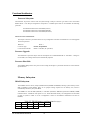
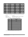
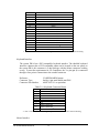
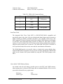
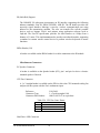
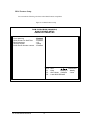
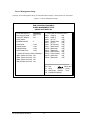
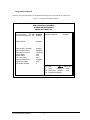
Advanced Pentium II Motherboard IN440EX USER’S MANUAL Copyright 1998 GVC CORPORATION. ALL RIGHTS RESERVED BCM Advanced Research 1 NOTICE Rights: No part of this manual, including but not limited to the products and software described in it, may be reproduced, transmitted, transcribes, stored in a retrieval system, or translated in any form or by any means without the expressed written permission of GVC “Corporation or BCM Advanced Research, Inc. Products and corporate names appearing in this manual may or may not be registered trademarks or copyrights of their respective companies and are used only for identification or explanation purposes without intent to infringe. ¨ ¨ ¨ ¨ Intel, MMX and Pentium are registered trademarks of Intel. IBM and OS/2 are registered trademarks of IBM. AWARD is a registered trademark of American Megatrends Inc. Winbond is a registered trademark of Winbond Electronics Inc. Responsibility: This manual is provided “As is” with no warranties of any kind, either expressed or implied, including, but not limited to the implied warranties or conditions of this product’s fitness for any particular purpose. In no event shall we be liable for any loss of profits, loss of business, loss of data, interruption of business, or indirect, special, incidental, or consequential damages of any kind, even the possibility of such damages arising from any defect or error in this manual or product. We reserve the right to modify and update the user manual without prior notice. BCM Advanced Research 2 COMPLIANCE & CERTIFICATE ISO 9001 Certificate: This device was produced in our plant with advanced quality system certified by DNV QA Ltd. in according to ISO 9001. This Certificate is valid for: DESIGN & MANUFACTURE OF MOTHER BOARDS AND PERSONAL COMPUTERS. CE Declaration: CE marking is a visible declaration by the manufacturer or his authorized representatives that the electrical equipment to which it relates satisfies all the provisions of the 1994 Regulations. FCC Compliance: FCC stands for Federal Communications Commission. This product complies with FCC Rules Part 15 and has been tested, and complied with the EMI rules by a certified body. In normal operation, there shall be no harmful interference caused by this device nor shall this devise accept any interference received, including interference that may cause undesired operation of this product. Microsoft Windows Compliance: Microsoft, Windows NT, Windows, and the Windows Logo are registered trademarks of Microsoft Corporation. BCM Advanced Research 3 EASY INSTALLATION The following “Easy Installation” steps are for users accustomed to the assembly of a computer system. For those individuals requiring more specific information please refer to the more detailed descriptions located within the latter chapters of this manual. Note: You must keep your power cable unplugged until the following installation steps are completed. Getting Start: Touch a grounded metal surface before unpacking your motherboard. For details please Install the CPU by correctly aligning the CPU with the as noted in the motherboard diagram. Once aligned, down on the CPU gently but firmly. Next, install either 3.3 volt unbuffered EDO or SDRAM into the 168 pin DIMMs. See Sec. 3.2 & Sec. 3.3. to release static electricity stored in your body refer to Precaution section in Chapter 3. Release Static Electricity Slot 1 press the Insert CPU & RAM After completing the above steps, install any expansion cards into the appropriate PCI, ISA or AGP slots and them tight to the chassis. See Sec. 3.4. Install All Expansion Slots Plug in all cables included in the package except for power cord. Please see Sec. 3.5. Please recheck all steps to ensure no mistakes have been made and then plug in the power cord and turn on the power to enter the BIOS setup, BCM Advanced Research screw the Couple Connectors Of HDD, FDD… Chapter 4. 4 CONTENTS FEATURES: 9 1 11 INTRODUCTION 11 Overview Processor Subsystem Cache Subsystem Memory Subsystem Data Integrity Subsystem A.G.P. Interface Embedded PCI Devices PCI Bus Master IDE PCI Add-in Cards Embedded A.G.P. Devices Embedded I/O Subsystem System Management Subsystem Advanced Configuration and Power Interface “ACPI” 11 11 11 12 12 12 13 13 13 13 13 13 13 2 34 FUNCTIONAL ARCHITECTURE 34 Processor Subsystem SLOT-1 Processor Socket Pinout Processor Upgrade Processor Heat Sink 34 34 34 34 Memory Subsystem DRAM Subsystem DRAM (DIMM) Sockets System BIOS 34 34 35 35 L2 Cache Subsystem Cacheable and Non-Cacheable Regions 35 35 Address Maps Memory Map I/O Address Map Interrupt Allocation DMA Channels 36 36 36 36 36 Video Subsystem 36 BCM Advanced Research 5 FEATURES 3D Accelerator Video Accelerator/Video Capture 2D Accelerator General Features Video Modes Video Memory Video (Monitor) Connector Sound Subsystem Sound Features Line Out Connector Microphone In Connector Line In Connector 3D Sound CD-IN Connector (Audio) Modem-In Connector 37 37 37 38 38 39 40 41 42 42 42 42 42 43 43 43 PCI/ISA Expansion Slots ISA Interface ISA/PCI Expansion Slots ISA Bus Speed AT Bus Refresh 43 43 43 44 44 Storage Subsystem IDE Hard Disk Drive Interface Floppy Disk Drive Interface 44 44 44 I/O Subsystem Serial Ports Parallel Port Keyboard Interface Mouse Interface Universal Serial Bus Connectors Real-Time Clock Non-volatile CMOS Memory Battery IR (Infra-Red) Support IRDA Header (J19) 45 45 46 47 47 48 49 49 50 50 Miscellaneous Connectors PC Speaker Connector CPU Fan Connector Hard Drive LED Connector Suspend (Sleep) Connector (J27) Power Button Switch (J29) Green/Power-on LED Connector Reset Button Connector (J30) 50 50 50 50 51 51 51 51 3 52 CONFIGURATION 52 Product Configuration 52 BCM Advanced Research 6 Processor Speed Select Jumper DRAM Subsystem Configurations 52 52 4 53 BIOS 53 The Main Menu Main Menu Selection Standard CMOS Setup Bios Feature Setup Power Management Setup Load BIOS Defaults Integrated Peripherals Supervisor Password User password Save & Exit Setup 55 56 58 60 62 63 64 65 65 65 5 66 ELECTRICAL AND MECHANICAL SPECIFICATIONS 66 Absolute Maximum Ratings 66 Electrical DC Specifications for 5V and 3.3V Signals 66 67 Power Supply Power Supply Connectors Input Power Budget 67 67 67 Mechanical System Interfaces User-Accessible Sockets Back-Panel Interfaces 68 68 68 68 Manufacturability/Serviceability 69 Regulatory 69 BCM Advanced Research 7 Photo Of the Motherboard Drawing of Motherboard I/O Back Plane PS/2 Key/Mouse Key/Mopuse USB BCM Advanced Research Parallel Serial GAME VGA Line Out 8 Line In Mic In FEATURES: Processor/Cache: Processor Intel “Deschutes”, “Klamath”, Celeron” Pentium II 233 ~ 333 MHz Operation with FSB (Front Side Bus) 66 MHz Slot 1 CPU Cartridge Integrated; Write Back and Write Through, direct mapped organization “BSB” Cache 0KB or 512KB Upgrades Cache Size System Memory Memory Size Memory Sites ECC/EC DIMM Type Memory Speed 8MB Min up to 256MB with Un-buffered SDRAM 2 DIMM Sockets. SDRAM. Auto-detect w/Table Free Configuration Double Density DIMMs. Non-ECC support. 8, 16, 32, 64 and 128MB. 64-bit non-ECC SDRAM 66Mhz parameter for synchronous memory. Chipset 82440EX AGP/PCI/ISA Chipset ISA/PCI Bus PCI Level 2.1. 33 MHz Zero Wait State Graphics Support “AGP” Video Memory ATI 3D Rage Pro Turbo 2X or Rage IIC, 66MHz AGP with sidebands and pipelining 64-bit PCI Graphics Accelerator. SGRAM @ 66MHz (128Kx32 or 256Kx32x2) Memory Capacity 2MB or 4MB on the motherboard, Integrated I/O I/O Controller Winbond W83977TF (Plug & Play Compliant) Serial Ports One 9 pin connectors for dual asynchronous serial ports. High speed 16C550 compatible serial ports. Infrared Interface Infrared port with FIR, IrDA and ASKIR Parallel Port One 25 pin supporting EPP, ECP and Centronics Interface Hard Disk Controller PCI Bus Mastering IDE. Native and Compatible Mode Support. IDE Transfer with Scatter Gather. “Ultra 33” Synchronous DMA. Enhanced IDE PIO mode 4 (16MB/s) Independent IDE timing. FIFOs for PCI Burst Transfers. Swap-Bay Support. Integrated 8x32-bit buffer for IDE PCI Burst Transfers Hard Disk Connector 2 PCI IDE Connectors for 4 Drives Support Floppy Controller 720 KB, 1.2, 1.44 and 2.88 MB support in non-FIR mode Keyboard Port PS/2 (Integrated in the FDC37C77X) Mouse Port PS/2 (Integrated in the FDC37C77X) Real Time Clock Integrated in the PIIX4 (DS1287 Compatible) System Monitor Winbond W83781D; Voltage/Temperature/Fan Speed/Chassis Intrusion External Communication Ports Serial Bus BCM Advanced Research Universal Serial Bus (USB), integrated with Core Logic 9 Integrated Sound Sound Chip CODEC FM Synthesis Sound Effects ESS Solo –1 Business Audio 16-bit Stereo ESFM™ Music Synthesiser 3D stereo effects System BIOS BIOS Type Hard Disk Driver Plug&Play Support Special Features Winbond based 2Mbit Flash IDE, Auto-configuring Steerable DMA Channels and Interrupts. ISA Plug&Play PC-98 ready. Multi-Boot. PCI Add-In cardauto- config. Green Features Power Management Advanced Features APM 1.2, ACPI (Advanced Configuration and Power Interface) compliant hardware for use with APM & PNP-BIOS APIs Jumpers and Front Panel Connectors Connectors Reset switch. Suspend/Resume Button. Speaker. HD & PWR LED. Power Button. IR. (Jumpers CPU Speed Multiplier. Password/CMOS Clear. Headers and Rear Panel Connectors Connectors Video. Parallel and Serial 1 Ports. Keyboard. Mouse. Line-Out. Mic., Line-In, game/midi USB 1&2 Serial 2. CPU Fan. Headers Headers and Connectors Connectors Headers None Floppy. IDE 1&2. CD-Audio In. Modem Audio. Aux-In. Reset switch. Speaker. Suspend/Resume Button. HDD & Power LED. Chassis Fan. Mechanical Board Style Board Size/Type MicroATX Form Factor 9.6” x 9.0”, Four Layer Board Expansion Slots Description BCM Advanced Research Two PCI Expansion connectors and two ISA Expansion connectors. 10 1 Introduction This section provides an overview for the MicroATX Pentium II based PCI/ISA Printed Wiring Assembly (PWA) code-named "IN440EX". It describes functional blocks and their relationship. The following diagram shows the functional blocks Overview The IN440EX is an implementation of BCM Advanced Research for a High-Volume MicroATX motherboard featuring these subsystems: • • • • • • • • • • Intel Pentium™ II MMX Processor cartridge support through the SLOT 1 connector Intel 82440EX PCIset: 82443EX (“PAC” PCI A.G.P. Controller) and 82371SB (“PIIX4” PCI-ISA-IDE Xcelerator) Accelerated Graphics Port “AGP” connector PCI IDE Bus Master interface Embedded advanced I/O support System Management Logic Advanced multiple Audio interface USB (Universal Serial Bus) System Monitoring Hardware MicroATX form-factor motherboard The targeted Operating Systems for the IN440EX are: Windows 95, Windows 98 and Windows NT. Processor Subsystem The IN440EX has provisions to support the following processors: Intel Pentium™ II Processor with MMX™ technology (Deschutes) operating at 333/66, 300/66, 266/66 and 233/66 MHz. The Processor speeds are selectable with a four, (4) jumper block combination for the bus-to-core frequency ratio and CPU bus speed. The bus-to-core ratio is either 2/7, 1/4, 2/9 or 1/5 yielding the bus/core frequency; 66/233, 66/266, 66/300 or 66/333 MHz respectively. High-performance features, including pipelined 32-bit addressing, 64-bit data, 16KB/16KB Instruction/Data Writeback or Write-through 2-way set associative primary cache. 0KB/512KB Write-back direct mapped secondary cache on the CPU Cartridge using a Back-Side-Bus (BSB). Two (2) Memory DIMM for support of SDRAM. Two onboard DC/DC converters supply the +2.5 Volts for the CPU I/O voltage and the +1.5 Volts GTL+ bus voltage (VTT). An on-board switching power converter supplies the CPU core voltage (VCORE), the switcher supports the Pentium II Voltage-ID pins for auto-voltage programming of the switcher supply. Cache Subsystem The cache and control functions are part of the Pentium II Processor. The cache SRAM interface is through the processor’s Back-Side-Bus (BSB) and is included within the CPU cartridge. The IN440EX can accept either the Pentium II cartridge with 512KB of second level (L2) Pipelined Burst SRAM cache. The Pentium II second level cache supports a direct mapped organization with a write-back policy, providing all necessary snoop functions and inquire cycles. Cacheability of the entire memory space in the first level cache is supported. For the second level cache only the first 512MB of main memory is cacheable, and only main memory controlled by the PAC DRAM interface will be cached, PCI and ISA memory is not cached. BCM Advanced Research 11 Memory Subsystem The IN440EX DRAM controller supports a 64-bit memory data interface, optionally supporting 64-bit wide DIMM modules, without ECC/EC. The DRAM types supported are Synchronous DRAM (SDRAM). SDRAM is supported at 66 MHz using symmetrical addressing. The IN440EX Main Memory interface provides two (2) 168-pin DIMM socket (DIMM0 and DIMM1) sites, allowing system memory from 8MB to 256MB of SDRAM. The DIMM sockets support either single or double-sided ‘Unbuffered DIMM’ modules. The installed DRAM type can be 8MB, 16MB, 32MB, 64MB or 128MB DIMMs. The DRAM Controller uses the JEDEC standard Serial Presence Detect (SPD) Mechanism to detect memory and array configurations, there is no jumper settings required for the memory size. Memory is automatically detected by the system BIOS. Rules for Populating the DIMM memory array • • DIMM sockets can be populated in any order. The DRAM Timing register, which provides the DRAM speed grade control for the entire memory array, will be programmed to use the timings of the slowest DRAMs installed. Data Integrity Subsystem Several data integrity features are included in the system. These are 64-bit DRAM interface for EX chipset, parity generation and checking on the PCI Bus and A.G.P. (for PCI transactions). PCI Bus. The system implements parity generation/checking as defined by the PCI specification. A.G.P. Bus. For the operations on the A.G.P. interface using PCI protocol, the system supports Parity generation/checking as defined by the PCI specification. Main Memory DRAM Protection Modes. The system supports three modes of data protection of the DRAM array: • Non-ECC with Byte-Wise Write Support (Default mode, in this mode there is no provision for protecting the integrity of data in the DRAM array.) A.G.P. Interface The A.G.P. is a high performance, component level interconnect targeted at 3D graphics applications and is based on a set of performance enhancements to PCI. The IN440EX is designed to support the A.G.P. Interface. The A.G.P. implementation is compatible with the Accelerated Graphics Port Specification. The system supports only a synchronous A.G.P. interface coupling to the host bus frequency. The actual bandwidth will be limited by the capability of the system’s memory, reaching the highest performance with fast SDRAM. The A.G.P. Interface supports PCI operations as defined by the PCI specification. Electrically, only 66MHz PCI operations are supported. BCM Advanced Research 12 For the definition of A.G.P. Interface functionality (protocols, rules and signalling mechanisms, as well as the platform aspect of A.G.P. functionality), refer to the latest A.G.P. Interface Specification. This document focuses only on the Controller specifics of the A.G.P. interface functionality. Embedded PCI Devices The PCI bus contains 1 embedded PCI device: PCI bus mastering IDE interface. The arbiter within the PAC performs arbitration for PCI bus masters. PCI Bus Master IDE PIIX-4 provides an integrated Bus Mastering IDE controller with two high performance IDE interfaces for up to four devices, such as Hard Drives and CD-ROM. PCI Add-in Cards High Performance PCI I/O cards can be used in the IN440EX through the PCI connector slots. The PCI bus is specified to support 10 loads. Each embedded controller or bridge (Video, PCI to ISA Bridge) count as 1 load, each PCI expansion slot used counts as 2 loads. To support multiple PCI devices in a single slot, add an expansion board containing PCI to PCI Bridge to a secondary PCI segment. Embedded A.G.P. Devices The AGP bus contains 1 embedded device: The ATI 3D Rage Pro Turbo 1X Graphics Accelerator. The 3D Rage Pro is a highly integrated graphics controller, integrating the 2D, 3D and video accelerators, palette DAC and quadruple clock synthesiser. Embedded I/O Subsystem The Winbond Plug and Play Ultra I/O controller “W83977TF” represents the newest technology in functionality and integration. While providing the standard PC I/O requirements the Ultra I/O complies with the ISA Plug-andPlay standard version 1.0a, and provides for the recommended functionality to support Windows 95. The Ultra I/O qualifies 16-bit address to allow relocation of 480 different addresses, with 13 IRQ options and 3 DMA channels available for each logical device. Other features of the Ultra I/O are: 8042 keyboard controller. An Infrared interface for Fast IR (FIR), IrDA and ASKIR. Floppy interface. Two serial ports with 16-byte FIFOs. One EPP/ECP supported bi-directional parallel port. System Management Subsystem The IN440EX support the System Monitor services using Winbond’s W83781D System Management chip. The W83781D is used to monitor Voltage, Temperature, Fan Speed and Open Case Intrusion. The combination of the System Monitor and the Wake On LAN (WOL) functionality achieves the Management Level 3. Advanced Configuration and Power Interface “ACPI” BCM Advanced Research 13 The IN440EX supports the ACPI specification and its key elements; The Operating System Directed Power Management (OSPM). ACPI evolves the existing collection of power management BIOS code, APM APIs, PNP BIOS APIs, and so on into a well-specified power management and configuration mechanism. It provides support for an orderly transition from existing (legacy) hardware to ACPI hardware, and it allows for both mechanisms to exist in a single machine and be used as needed. ACPI evolves the existing motherboard configuration interfaces to support these advanced architectures in a more robust, and potentially more efficient manner. OSPM provides a new appliance interface to customers. In particular, it provides for a sleep button. This sleep button is a “soft” button, which does not turn the machine physically off but signals the OS to go into a ‘soft off’ or sleeping state. ACPI defines two types of these “soft” buttons: one for putting the machine into sleep mode and one for putting the machine into ‘soft off’ mode. This gives the OEM two different ways to implement machines: A one or a two-button model. The button on the one-button model can be used as a power button or a sleep button as determined by user settings. The two-button model has an easily accessible sleep button and a separate power button. In either model, an override feature that forces the machine to turn off or to reset without OS consent is also needed to deal with various rare, but problematic, situations. ACPI is neither a software nor a hardware specification, although it addresses both software and hardware and how they must behave. ACPI is actually an interface specification. BCM Advanced Research 14 Functional Architecture Processor Subsystem The Pentium II processor connects with the system through a 242-pin connector type socket on the circuit board labelled SLOT-1. The 242-pin configuration corresponds to a standard pinout that can accommodate the following processors: Intel Pentium™ II Processor with MMX (Celeron) Intel Pentium™ II Processor with MMX (Klamath) Intel Pentium™ II Processor with MMX (Deschutes) SLOT-1 Processor Socket Pinout The 242-pin connector is provided to allow for easy configuration at the time of manufacture or as a field upgrade of the microprocessor. Reference: Connector Type: Connector Part Number: SLOT-1 Female, 242 pin Dimm Molex 71796-0001 (Or equivalent) Processor Upgrade The Pentium™ II processor maybe removed and replaced to accommodate Kamath or “Deschutes”. Changes to the VCORE (Core Voltage Selection) are automatically adjusted. Processor Heat Sink The IN440EX M/B provides 12V power for the cooling fan through a 3-pin header with Fan-On control and Fan Speed detection. Memory Subsystem DRAM Subsystem The IN440EX has two 64-bit (168-pin) DIMM sockets (DIMM0 and DIMM1) allowing system memory from 8 MB to 256MB of main DRAM. There are no jumpers settings required for the memory size, which is automatically detected by the system BIOS. The DIMMs are rated 66 MHz (Klamath) or 100 MHz (Deschutes) SDRAM (Synchronous DRAM). DIMM modules must be ‘Unbuffered’ and operate at 3.3V. All the allowable memory size configurations are described on table 2.1 (Refer to Table 3.6 in the “Configuration” section for the different combinations and sizes of DIMMs). Table 2.2. DRAM memory configurations in Megabytes. 8 64 144 16 72 176 24 80 192 BCM Advanced Research 32 96 256 40 128 48 136 34 DRAM (DIMM) Sockets Connection to the main system DRAM can be done via two (2) DIMM connectors on the system PWA. Reference: Connector Type: Connector Part Number: DIMM0, DIMM1 female, 168 pin DIMM, in-line connector Berg. 91145-60024 (Or equivalent) System BIOS The system and video BIOS are stored in a 2M-bit (256Kx8) Flash Memory device. The system BIOS is always shadowed and cached. L2 Cache Subsystem The Pentium II processor cartridge provides an unified 0KB or 512KB second level (L2) cache to complement the level one data and instruction (L1) internal caches. The L2 cache is Direct-Mapped non-sectored, supporting the Write Back policy architecture. Table 2.4. L2 Cache latency with Burst SRAM Cycle Type Clock Count Burst Read X-1-1-1 Burst Write (Write-back) X-1-1-1 Single Read X Single Write X Pipelined Back-to-Back Burst Reads X-1-1-1,1-1-1-11 1 : The back-to-back cycles do not account for CPU idle clocks between cycles Cacheable and Non-Cacheable Regions The system caches the following regions: • • All system memory, including 0 to 640 KB and all memory present above 1 MB up to 1GB. System and integrated video controller BIOS. The system does not cache the following regions: • The video memory block from A0000 to BFFFF. BCM Advanced Research 35 • • PCI memory space on top of main memory. Any access to the PCI or AT bus. Address Maps Memory Map The following table describes the breakdown of the IN440EX memory areas and how they are assigned. Table 2.5. Memory Map LOCATION 0FFFFFFF-FFFFFFFF 000E0000-000FFFFF 000C8000-000DFFFF 000C0000-000C7FFF 000A0000-000BFFFF 00080000-0009FFFF 00000000-0007FFFF SIZE 256MB 128KB 96KB 32KB 128KB 128KB 512KB TO 4GB 1MB 896KB 800KB 768KB 640KB 512KB DESCRIPTION BIOS ROM System BIOS (Shadowed in DRAM) Expansion region (Shadowed in DRAM) Video BIOS (Shadowed in DRAM) Video Buffer (SMM space Non-Cacheable) Optional memory space gap (DOS Apps) DOS applications (No read/write protect) (Always cacheable) Video Subsystem 3D RAGE PRO Graphics Controller is a highly integrated graphics controller. Incorporated within this single chip are the 2D, 3D and video accelerators, palette DAC, and quadruple clock synthesiser. This multi-function integrated controller delivers superior 3D performance, TV-quality scaled video optimized for MPEG playback, industry-leading Mach64 2D performance, and video expansion capability suited for video conferencing, cable TV viewing, and hardware MPEG decoding. The availability of ATI BIOS, drivers, utilities, and application software developed for the entire chip family is a major strength for the 3D RAGE PRO. Being register-compatible with all other controllers in the Mach64 accelerator series means immediate compatibility with a wide range of application drivers. Since this controller is also pin-compatible with ATI's family of other mach64 integrated controllers, it provides to the OEM a low-cost upgrade path to additional features and performance. This controller uses active power management techniques to monitor activity levels within its’ self and to perform real-time power reductions such as dynamic clock control and graphics engine shutdown. Because full-speed operation can be restored without delay, these techniques do not impact performance. Major advances have been included in this chip to boost performance in the area of a new bus interface, Accelerated Graphics Port BCM Advanced Research 36 (AGP). With AGP data the throughput between host and 3D RAGE PRO has greatly increased. The result is even faster 2D and 3D performance and enhancements to motion video support (e.g. MPEG-2 motion compensation). FEATURES 3D Accelerator • • • • • • • • • • Complete 3D primitive support: points, lines, triangles, lists, strips and Quadrilaterals Triangle Setup Engine with floating point to integer parameter conversion 4K on-chip Texture Cache Destination Alpha Gouraud shading Alpha blending and alpha interpolation 16-bit Z buffer Fogging and fog interpolation Dithering support in 16 bpp for near 24 bpp quality Perspectively correct mip-mapped texture mapping hardware, supporting: • Palletized CI4 and CI8 texture expansion • Texture filtering models including tri-linear mip mapping • Texture lighting modes • Ability to use YUV format textures • Alpha in texture map • Texture maps up to 1024 x 1024 • Non square texture maps Software driver support for Direct 3D, QuickDraw 3D RAVE and OpenGL interfaces, as well as others. Video Accelerator/Video Capture • • • • • • • • • Back end scaling Color interpolation during scaling for improved high resolution video quality Integrated 768 pixel wide dual video line buffers support filtered video scaling 4 tap horizontal and 2 tap vertical scalers for high-quality, full-screen video playback with MPEG-2 (720x480) sources YUV to ROB color space conversion with support for both packed and planar YUV formats as follows: • YUV422, YUV410 (YUV9), YUV420 (YUV12) • RGB32, RGB16/15 Built-in continuous brightness and gamma correction to correct 'dark' images Chroma keying for effective overlay of video on graphics Overlay true color video regardless of the current graphics mode New buffer and frame synchronization modes to reduce display tearing BCM Advanced Research 37 • • • • Ability to turn off graphics data access behind video, hence reducing bandwidth Support for CCIR 656 video standard Ability to capture VBI and Intercast data Mirror video capture to support video conference 2D Accelerator • • • • • • • • • • • Hardware acceleration - Rectangle Fill, Line Draw, BitBlt, Polygon Fill,Panning/Scrolling, Bit Masking, Monochrome Expansion, Scissoring, and full ROP support PCI bus master support for GUI programming 8x8x8 SRC Brush support Quick engine setup with alias registers Improved FIFO management to memory controller Increased command FIFO to 128 DWORDs Hardware cursor up to 64x64x2 Acceleration provided in 8/l6/24/32bpp modes. Packed pixel support (24bpp) enables true color in 1MB configurations Game acceleration for Microsoft's DirectDraw—Double Buffering, Virtual Sprites, Transparent Blit and Masked Blit Increased display FIFO to 32 DWORDs. Additional 64 entry FIFO for Bus mastering True 24-bit, true-color palette DAC: • Pixel clock rates up to 200MHz, with 230MHz option, for up to 1600x1200 screen resolution at 85Hz vertical • Pixel depth of 32 bit at 1600x1200 screen resolution with WRAM and external RAMDAC at 240 MHz • Gamma correction for true WYSIWYG • Full 24-bit palette General Features • • • • • • • Integrated 3D, 2D, and Video accelerators with palette DAC and quad-clock synthesiser in a single chip Comprehensive AGP support, including 66 MHz and 133 MHz pipeline operation with sideband addressing PCI revision 2.1 bus for Plug-and-Play ease of use Bi-endian support for compliance on a variety of processor platforms 128-level command FIFO assures fast response to host command transfers for maximum CPU/host bus/controller efficiency and concurrent operation Additional 64 entry FIFO dedicated to Bus mastering Programmable flat or paged memory model with enhanced host access to a linear frame buffer BCM Advanced Research 38 • • • • 32-bit wide read/writeable memory mapped registers with optimized organization, reduces instruction overhead and raises performance DDC1 and DDC2B+ Plug-and-Play monitor support Power management for full VESA Display Power Management Signalling(DPMS) and EPA Energy Star compliance. Also, register support for controller power reduction and DAC power down Built-in CRC, chip diagnostics and manufacturing SCAN to ensure quality components Video Modes The following video modes are supported on the system board by the ATI-3D Rage Pro Graphics and Video Controller Table 2.9. Video Modes Display Re-fresh Hor. Screen Rate Scan Resolution (kHz) 640x480 640x480 640x480 640x480 640x480 640x480 800x600 800x600 800x600 800x600 800x600 800x600 800x600 800x600 800x600 1024x768 1024x768 1024x768 1024x768 1024x768 1024x768 1024x768 1024x768 1152x864 60 72 75 90 100 120 48 56 60 70 72 75 90 100 120 43 60 70 72 75 90 100 120 43 31.4 37.7 37.5 47.9 52.9 63.7 33.8 35.1 37.8 44.5 48.0 46.8 57.0 62.5 76.0 35.5 48.3 56.4 58.2 60.0 76.2 79.0 96.7 45.9 Pixel Clock (MHz) 25.2 31.2 31.5 39.9 44.9 55.0 36.0 36.0 40.0 44.9 50.0 49.5 56.6 67.5 81.0 44.9 65.0 75.0 75.0 78.8 100 110 130 65.0 Colors (Bits per Pixel) 4 √ √ √ √ √ √ √ √ √ √ √ √ √ √ √ √ √ √ √ √ √ BCM Advanced Research 1 MB DRAM 8 16 24 √ √ √ √ √ √ √ √ √ √ √ √ √ √ √ √ √ √ √ √ √ √ √ √ √ √ √ √ √ √ √ √ √ 32 - 4 √ √ √ √ √ √ √ √ √ √ √ √ √ √ √ √ √ √ √ √ √ √ √ 2 MB DRAM 8 16 24 √ √ √ √ √ √ √ √ √ √ √ √ √ √ √ √ √ √ √ √ √ √ √ √ √ √ √ √ √ √ √ √ √ √ √ √ √ √ √ √ √ √ √ √ √ √ √ √ √ √ 39 32 √ √ √ √ - 4 √ √ √ √ √ √ √ √ √ √ √ √ √ √ √ √ √ √ √ √ √ √ √ √ 4 MB DRAM 8 16 24 32 √ √ √ √ √ √ √ √ √ √ √ √ √ √ √ √ √ √ √ √ √ √ √ √ √ √ √ √ √ √ √ √ √ √ √ √ √ √ √ √ √ √ √ √ √ √ √ √ √ √ √ √ √ √ √ √ √ √ √ √ √ √ √ √ √ √ √ √ √ √ √ √ √ √ √ √ √ √ √ √ √ √ √ √ √ √ √ √ √ √ √ √ √ √ 1152x864 1152x864 1152x864 1152x864 1152x864 1152x864 1280x102 4 1280x102 4 1280x102 4 1280x102 4 1280x102 4 1280x102 4 47 60 70 75 80 85 43 44.8 54.9 66.1 75.1 75.1 77.1 50.0 65.0 80.0 100 110 110 121.5 80.0 √ √ √ √ √ - - - - √ √ √ √ √ √ √ √ √ √ √ √ √ √ - - - √ √ √ √ √ √ √ √ √ √ √ √ √ √ √ √ √ √ √ √ √ √ √ √ √ √ √ √ √ - 47 50.0 80.0 √ - - - - √ √ - - - √ √ √ √ - 60 69.3 110 - - - - - √ √ - - - √ √ √ √ - 70 74.6 126 - - - - - √ √ - - - √ √ √ √ - 74 78.8 135 - - - - - √ √ - - - √ √ √ - - 75 79.9 135 - - - - - √ √ - - - √ √ √ - - Video Memory The system’s video memory consists of SGRAM only. In it’s standard configuration, the system will have two 256K/512Kx32 SGRAM chips soldered on the board to give a total of 2MB/4MB. Pin # 1 3 5 7 9 11 13 15 17 19 21 23 25 27 29 31 33 35 37 39 41 43 Table 2.10. SO-DIMM Video Memory Module Connector Pinout Description Pin # Description Pin # Description Pin # Description GND 2 GND 73 MCK 74 MCK VMD63 4 VMD62 75 VCC 76 VCC VMD61 6 VMD60 77 NC 78 NC VMD59 8 VMD58 79 GND 80 GND VMD57 10 VMD56 81 VMA9 82 VMA8 VCC 12 VCC 83 VMA7 84 VMA6 VMD55 14 VMD54 85 GND 86 GND VMD53 16 VMD52 87 VMA5 88 VMA4 VMD51 18 VMD50 89 VMA3 90 VMA2 VMD49 20 VMD48 91 VMA1 92 VMA0 GND 22 GND 93 VCC 94 VCC DQM#7 24 DQM#6 95 VMD31 96 VMD30 DQM#5 26 DQM#4 97 VMD29 98 VMD28 VCC 28 VCC 99 VMD27 100 VMD26 VMD47 30 VMD46 101 VMD25 102 VMD24 VMD45 32 VMD44 103 GND 104 GND VMD43 34 VMD42 105 VMD23 106 VMD22 VMD41 36 VMD40 107 VMD21 108 VMD20 GND 38 GND 109 VMD19 110 VMD18 VMD39 40 VMD38 111 VMD17 112 VMD16 VMD37 42 VMD36 113 VCC 114 VCC VMD35 44 VMD34 115 DQM#3 116 DQM#2 BCM Advanced Research 40 45 VMD33 46 VMD32 47 VCC 48 VCC 49 NC 50 NC 51 NC 52 NC 53 NC 54 NC 55 GND 56 GND 57 DSF 58 NC 59 NC 60 NC 61 NC 62 NC 63 VCC 64 VCC 65 SO_CS166 SO_CS067 RAS#0 68 CAS#0 69 WE# 70 CKEX 71 GND 72 GND Video (Monitor) Connector 117 119 121 123 125 127 129 131 133 135 137 139 141 143 DQM#1 GND VMD15 VMD13 VMD11 VMD9 VCC VMD7 VMD5 VMD3 VMD1 GND SDA(21,22) VCC 118 120 122 124 126 128 130 132 134 136 138 140 142 144 DQM#0 GND VMD14 VMD12 VMD10 VMD8 VCC VMD6 VMD4 VMD2 VMD0 GND SCL (22) VCC Connection to VGA monitor is via a connector on the rear panel on the system PWA. Reference: Connector Type: Connector Part Number: J8 (Video) female, high density DB15S, 15-pin AT-compatible Foxconn Dz11AA1B8 or equivalent Table 2.11. Video Monitor Connector Pinout PIN 1 2 3 4 5 6 7 8 9 10 11 12 13 14 15 16 17 1: Description RED GREEN BLUE N/C LOGIC-GROUND RED GROUND RETURN GREEN GROUND RETURN BLUE GROUND RETURN +5V PULL-UP LOGIC GROUND N/C DDC DAT HORIZONTAL-SYNC VERTICAL-SYNC DDC CLK LOGIC-GROUND1 LOGIC-GROUND1 Pins 16 and 17 are connector mounting holes connected to logic ground. BCM Advanced Research 41 Sound Subsystem The IN440EX uses the ESS Solo-1 (ES1938), which is a single chip multimedia audio system controller. It includes an integrated FM synthesiser and a Plug and Play PSI interface. The ES1938 is compatible with the Microsoft Windows Sound System standard and will run software written to the Sound Blaster and Sound Blaster Pro interfaces. Sound Features • • • • • • • • Compatible with Sound Blaster™, Sound Blaster Pro™, and Windows Sound System™, PC97/PC98 and WHQL specifications. High-Quality ESFM™ Music Synthesiser. Fully Plug-and-Play PCI Compatible Integrated Spatializer® 3D Audio Effects Processor. 16-Bit Address Decode Support 4248 Register Compatible Dynamic Range (SNR) Over 80dB ACP1 Compliant Line Out Connector The audio subsystem provides external sound through a user accessible stereo jack connector (J5-1) soldered to the PWA. This jack will allow the connection of selfamplified speakers. Reference: Connector Type: Connector Part Number: J5-1 (LINE OUT) 1/8 in. Audio Jack Connector Singatron, SJ-500C-0 (or equivalent) Microphone In Connector An external accessible jack connector (J5-3) is soldered to the PWA to allow the connection of a microphone for voice input. Reference: Connector Type: Connector Part Number: J5-3 (MIC IN) 1/8 in. Microphone Jack Connector Singatron, SJ-500C-0 (or equivalent) Line In Connector An external accessible jack connector (J5-2) is soldered to the PWA to allow the connection of a Line-In for line input. BCM Advanced Research 42 Reference: Connector Type: Connector Part Number: J5-2 (Line-In) 1/8 in. Line-In Jack Connector Singatron, SJ-500C-0 (or equivalent) 3D Sound The ESS Solo-1 has integrated the 3D Audio Effects processor which uses technology from Spatializer® Audio Laboratories, Inc., and expands the sound field emitted by two speakers to create a resonant 3D sound environment. CD-IN Connector (Audio) Access to the CD-IN connector for audio input from CD-ROM drives. Modem-In Connector Access to the MODEM-IN connector for audio input and output from the phone connection. PCI/ISA Expansion Slots ISA Interface The IN440EX incorporates a fully ISA (AT) bus compatible master and slave interface that is compatible with the IEEE 996 specification. The ISA interface also provides byte swap logic and I/O recovery support. The ISA interface supports the following types of cycles: • • • • • PCI master-initiated I/O and memory cycles to the ISA bus DMA compatible cycles between main memory and ISA I/O and between ISA I/O and ISA memory Enhanced DMA cycles between PCI memory and ISA I/O ISA refresh cycles initiated by either the controller or an external master ISA master-initiated memory cycles to PCI and ISA master-initiated I/O cycles to the controller registers ISA/PCI Expansion Slots BCM Advanced Research 43 The IN440EX motherboard support ISA and PCI expansion buses to implement up to two (2) ISA and two (2) PCI slots. The IN440EX will support one (1) ISA, one (1) PCI and one (1) shared ISA/PCI NLX slot. ISA Bus Speed Dividing the PCI clock by 4 generates the ISA system clock. The divide by 4 setting is used for 30MHz and 33MHz PCI bus speed. The frequencies supported are 7.5MHz and 8.33MHz. AT Bus Refresh The IN440EX system board supports hidden refresh cycles which allows the CPU to continue to execute unless an AT bus cycle is attempted coincident with the AT bus refresh cycle (ISA Bus refresh cycles are completely decoupled from DRAM Refresh). Transactions driven by PCI masters that target ISA or IDE resources while refresh is active are held off with wait states until the refresh is complete. Storage Subsystem IDE Hard Disk Drive Interface The IN440EX provides two (2) independent high performance bus-mastering PCI IDE interfaces capable of supporting PIO Mode 3, Mode 4 and ‘Ultra33’ Synchronous DMA mode devices. The integrated IDE interface can control up to four IDE devices allowing for both CD-ROM and Hard Disk drives. IDE PRI & IDE SEC are the primary and secondary IDE connectors respectively. Both IDE controllers can be disabled through BIOS to allow for external disk drive controllers. Floppy Disk Drive Interface The IN440EX has an integrated 765B compatible floppy disk controller using the Winbond’s W83977TF component. The FDC sub-section can control one (720KB, 1.2, 1.44 or 2.88MB) floppy disks or compatible tape drives. The floppy I/O address can be relocated to 480 different locations. 13 IRQ and 3 DMA channel options are available as well. Includes multiple power down modes for reduced power use. The floppy disk interface contains 48mA drivers and Schmitt trigger inputs on the drive interface. BCM Advanced Research 44 I/O Subsystem The I/O Subsystem consists of a single component from Winbond. The IN440EX uses the Plug and Play Compatible Ultra I/O Controller “W83977TF”, this device provides support for the ISA Plug-and-Play version 1.0a and includes the recommended functionality to support Windows 95. Through internal configuration registers, each of the W83977TF’s logical device’s I/O address, DMA channel and IRQ channel may be programmed. There are 480 I/O address location options, 13 IRQ options and 3 DMA channel options for each logical device. The Ultra I/O device provides two (2) high speed UARTs compatible serial ports with send/receive 16 Byte FIFOs or one IR port, one Multi-Mode Parallel Port with ECP/EPP modes, and a Floppy/Tape Controller supporting up to 2.88MB transfer rates. Serial Ports The IN440EX has two (2) UARTs compatible serial ports configured as Data Terminal Equipment (DTE). The electrical characteristics are compliant with the EIA-232-D Serial Communications Specifications. The serial ports may be remapped above other installable serial ports or disabled through BIOS. As a minimum the first serial port (COM1) must be capable of re-mapping to COM3. The second serial port (COM2) must be able to be remapped to COM4. The serial ports I/O address can be relocated within 480 different locations. The default address for COM1, COM2, COM3 and COM4 are 3F8H, 338H, 2F8H and 238H respectively. 13 different IRQ options are available to the serial ports. One port (COM1) is available through a connector (J4) is located on the rear panel of the system PWA. The second Serial Port (COM2) is available through a header on the PWA. Reference: Connector Type: Connector Part Number: J4 (COM1) male, 9 pin metal shell D-SUB Amp 1-103322-5 or equivalent Reference: Connector Type: Connector Part Number: J13 (COM2) male, 2x5, 0.100” centerline, straight Amp 1-103322-5 or equivalent BCM Advanced Research 45 Table 2.17. Serial Port Connector Pinout. PIN 1 2 3 4 5 6 7 8 9 10 11 DESCRIPTION DATA-CARRIER-DETECT (DCD) RECEIVE-DATA (RXD) TRANSMIT-DATA (TXD) DATA-TERMINAL-READY (DTR) LOGIC-GROUND DATA-SET-READY (DSR) REQUEST-TO-SEND (RTS) CLEAR-TO-SEND (CTS) RING-INDICATOR (RI) SHELL-GROUND1 SHELL-GROUND1 1: Pins 10 and 11 (Shell Ground) are mounting holes connected to the metal connector housing on serial port 1. Parallel Port The system PWA has a single, bi-directional parallel port (EPP/ECP compatible). The parallel port is capable of being disabled or remapped to either the secondary LPT address or the tertiary LPT address through BIOS if other parallel ports are installed in the system. The parallel port I/O address can be relocated within 480 different locations. Three (3) DMA channels options and 13 different IRQ options are available to the parallel port. A connector is located on the rear panel of the system PWA for the external connection to the port. The parallel port interface contains 12mA source output drivers on the drive interface, and incorporates ChipProtect circuitry for protection against damage due to printer Power-On. Reference: Connector Type: Connector Part Number: J7 (PARALLEL) female, 25 pin metal shell D-SUB AMP 750096-3 or equivalent Table 2.18. Printer Port Connector Pinout PIN 1 2 3 4 5 6 7 8 9 BCM Advanced Research DESCRIPTION STROBE* PD0 PD1 PD2 PD3 PD4 PD5 PD6 PD7 46 10 11 12 13 14 15 16 17 18 19 20 21 22 23 24 25 26 27 ACKNOWLEDGE* BUSY PAPER-END (PE) SELECT AUTO-FEED* ERROR* INIT* SELECT -IN* LOGIC-GROUND LOGIC-GROUND LOGIC-GROUND LOGIC-GROUND LOGIC-GROUND LOGIC-GROUND LOGIC-GROUND LOGIC-GROUND SHELL-GROUND1 SHELL-GROUND1 1: Pins 26 and 27 are connector-mounting holes connected to the metal connector housing. Keyboard Interface The system PWA has a PS/2-compatible keyboard interface. The shielded keyboard interface connector has a PS/2-compatible pinout and is located on the rear panel on the system PWA, this connector is a dual package with the Mouse connector residing on top. To meet the requirements for UL compliance, the Vcc pin (pin 4) is connected through a fuse prior to connection to the external connector. Reference: Connector Type: Connector Part Number: J2 (KEYBOARD) bottom female, 6-pin metal shield mini-DIN AMP 749231-1 or equivalent Table 2.19. Keyboard Connector Pinout PIN 1 2 3 4 5 6 7 8 9 DESCRIPTION KEYBOARD-DATA N/C LOGIC-GROUND KEYBOARD-Vcc KEYBOARD-CLOCK N/C SHELL-GROUND1 SHELL-GROUND1 SHELL-GROUND1 1: Pins 7-9 are, connector-mounting hole pins connected to the metal connector housing Mouse Interface BCM Advanced Research 47 The system PWA has a PS/2-compatible mouse interface. The shielded mouse port can be disabled through SETUP. A connector, utilizing PS/2 pinouts, is located on the rear panel on the system PWA. To meet the requirements for UL compliance the Vcc pin (pin 4) was connected through a fuse prior to connection to the external connector. Reference: Connector Type: Connector Part Number: J2 (MOUSE) Top female, 6-pin metal shield mini-DN AMP 749231-1 or equivalent Table 2.20. Mouse Connector Pinout PIN 1 2 3 4 5 6 7 8 9 DESCRIPTION MOUSE-DATA N/C LOGIC-GROUND MOUSE-Vcc MOUSE-CLOCK N/C SHELL-GROUND1 SHELL-GROUND1 SHELL-GROUND1 1: Pins 7-9 are connector-mounting hole pins connected to the metal connector housing. Universal Serial Bus Connectors The Universal Serial Bus (USB) is a communications architecture that gives a PC the ability to interconnect a variety of devices via a simple four-wire cable. The USB is actually a two-wire serial communication link that runs at 12 megabits (Mbs) per second. USB protocols can configure devices at startup or when they are plugged in at run time. These devices have been broken into five major classes: • • • • • Monitors Communication devices Audio Human input Mass storage More classes will be identified as the USB Standard matures. The IN440EX is equipped with two USB Serial Ports. This permits connection of two USB peripheral devices directly to the system without an external hub. If more devices are needed, an external hub can be connected to either of the built-in ports. Reference: BCM Advanced Research J3, (USB-1) + USB2 48 Connector Type: Connector Part Number: USB CONN, DUAL Molex, 87525-001 or equivalent Table 2.21. USB-1 & 2 Connector Pinout PIN DESCRIPTION COMMENT 1 VCC Cable power 2 - Data 3 + Data 4 Ground Cable ground Real-Time Clock The integrated Real Time Clock (RTC) is DS12887/MC146818 compatible and provides the time of day clock, 100-year calendar with alarm features and is accurate to within 1 minute per month, it consumes less than 1 µA of standby current (Typ.). The (RTC) supports 256 bytes of battery backed Non-volatile CMOS memory in two banks of 128 bytes each, both banks being reserved for BIOS use. One bank of CMOS memory is used to maintain the clock and user-system-setting configuration parameters when the main system power is removed. The other bank (128 bytes) is lockable in 4x32 byte blocks and can be used to store and lock miscellaneous information. The CMOS RAM can be set to specific values or cleared to the system default values using the BIOS SETUP program. Also to prevent a lock-up situation the CMOS RAM values can be cleared to the system defaults by using the CLR CMOS jumper on the PWA. Non-volatile CMOS Memory Battery An external coin-cell style battery provides power to the RTC and CMOS memory when system power is removed. The battery has an estimated lifetime of five to seven years and is socketed for easy replacement. Reference: Socket Type: BCM Advanced Research BT1 COIN TYPE 49 IR (Infra-Red) Support The IN440EX I/O subsystem incorporates an IR interface supporting the following industry standards; Fast IR, IRDA (HP-SIR), ASK-IR. The IR header provides the necessary signal interface allowing a two-way wireless communication port using infrared as the transmission medium. The user can transfer files to/from portable devices such as laptops, PDA’s and printers using application software such as LapLink. The Fast IR specification provides for data transfers at 4 Mbps from a distance of 1 meter. This implementation also provides an infrared interface supporting a standard or custom remote control device to perform wireless keyboard or mouse functions. IRDA Header (J19) A header is available on the IRDA header for a cable connection to the IR module. Miscellaneous Connectors PC Speaker Connector A header is available on the Speaker header (J22), pin 1 and pin 4 to drive a chassismounted speaker if desired. CPU Fan Connector A 1 x 3 straight header is available on the PWA to drive the CPU mounted cooling fan and provide the system with the Fan’s tachometer input. Reference: Connector Type: Connector Part Number: J18 (FAN) 1 x 3 male straight 0.100 AMCO 463-2-03 or equivalent Table 2.24. CPU Fan Conn. Pinout PIN 1 2 3 SIGNAL LOGIC-GROUND FAN-PWR-ON FANTACH3 Hard Drive LED Connector BCM Advanced Research 50 A header is available on the primary IDZ connector (J32) and secondary IDZ connector (J28) to power an LED on the front panel to indicate hard drive activity. Suspend (Sleep) Connector (J27) A header is available on the Sleep Header (J27) for connecting a momentary contact switch on the front panel, which can be used to turn the system into Sleep Mode. Power Button Switch (J29) A header is available on the power button header (J29) for connecting a momentary contact switch on the front panel, which can be used to turn the system power off or on. Green/Power-on LED Connector A header is available on the Green LED (J22, pin 2 and pin 4) for connecting to a Green LED or Power-on indicator (J23). Reset Button Connector (J30) A header is available on the Reset header (J30) for connecting a momentary contact switch on the front panel, which can be used to reset the system. BCM Advanced Research 51 3 Configuration Product Configuration The PWA component will be produced by BCM without the microprocessor installed, it is assumed that the microprocessor will be installed during the customer’s integration process. The same applies to the system memory DRAM DIMMs. Processor Speed Select Jumper To select the processor speed there is a jumper block of user-accessible jumpers labeled “JP1”. To select the processor speed install the jumper as follows: Table 3.1. CPU Speed Selection Klamath CPU Speed (MHz) 233 266 300 333 1-2 3-4 5-6 7-8 ON OFF OFF OFF OFF ON ON OFF ON ON ON ON OFF ON OFF ON DRAM Subsystem Configurations The IN440EX supports 8 MB to 256MB of system RAM. The allowable memory configurations are shown below: Table 3.2. DIMMs Configurations DIMM0 DIMM1 Total Memory 8MB 8MB 16MB 16MB 16MB 32MB 32MB 32MB EMPTY 8MB EMPTY 8MB 16MB EMPTY 8MB 16MB 8MB 16MB 16MB 24MB 32MB 32MB 40MB 48MB BCM Advanced Research 52 32MB 64MB 64MB 64MB 64MB 64MB 128MB 128MB 128MB 128MB 128MB 128MB 32MB EMPTY 8MB 16MB 32MB 64MB EMPTY 8MB 16MB 32MB 64MB 128MB 64MB 64MB 72MB 80MB 96MB 128MB 128MB 136MB 144MB 176MB 192MB 256MB For simplicity other memory configurations were not included on this table. BCM Advanced Research 53 4 Bios Software This product’s software is referred to as “BIOS” (Basic Input and Output Subroutine), the BIOS resides as firmware in a non-volatile memory device using Flash technology. This technology gives the user the ability to be able to update the BIOS and accommodate changes to features or optimizations to better the performance of the system. The user need only to load a diskette with the new BIOS firmware and follow the manufacturer instructions to update the BIOS. General This product will have an Award Software, Inc. developed system Flash BIOS. The BIOS will have a menu driven SETUP utility. The specific features & implementation requirements are to be provided by the OEM Customer if so desired. BIOS Setup The SETUP Menu on your BIOS maybe slightly different than the one represented in here. Different OEMs will require certain user access to advanced functions while other OEMs may not allow the user any access at all. The exact BIOS Menu representation can be extracted from the BIOS supplied with your platform. BCM Advanced Research 54 The Main Menu To start the Award BIOS CMOS Setup utility: 1.Turn on or reboot your system. The Award BIOS displays this message at the bottom of the screen: Press DEL to enter SETUP 2. Press the DELete Key to display the Main Menu, which looks like this: Figure 4.1. BIOS Setup Main Menu ROM PCI/ISA BIOS (2A59GB3J) CMOS SETUP UTILITY AWARD SOFTWARE, INC. STANDARD CMOS SETUP INTEGRATED PERIPHERALS BIOS FEATURES SETUP SUPERVISOR PASSWORD POWER MANAGEMENT SETUP USER PASSWORD LOAD BIOS DEFAULTS SAVE & EXIT SETUP Esc : Quit F10 : Save & Exit Setup : Select Item (Shift)F2 : Change Color Time, Date, Hard Disk Type... BCM Advanced Research 55 Main Menu Selections The Main Menu Selections are as follows: Standard CMOS Setup BIOS Features Setup Power Management Setup Load BIOS Defaults Integrated Peripherals Supervisor Password User Password Save & Exit Setup Table 4.1. Main Menu Selections Use this menu for basic system configuration, such as Date, Time, Hard Drive Parameters and Floppy Drive Parameters. Use this menu to set certain BIOS Features available on your system's chipset. Use this menu to configure Power-Management features. Use this to load the BIOS Defaults, except the Standard CMOS Setup Use this menu to configure the Onboard peripherals, such as Serial and Parallel Ports and Hard Drive and Floppy Drive Controllers. Setting a Supervisor Password restricts access to the BIOS Setup menus Setting a User Password restricts access to the BIOS Setup menus or the System Save all changes to CMOS and Exit the Setup Utility Use the “←↑→↓” arrow keys to make a selection. BCM Advanced Research 56 Standard CMOS Setup You can make the following selections on the Standard CMOS Setup Menu. Figure 4.1.1 Standard CMOS Setup ROM PCI/ISA BIOS (2A59GB3J) STANDARD CMOS SETUP AWARD SOFTWARE, INC. Use the table on the following page to configure the features on the standard CMOS Setup Men Date (mm:dd:yy) : Wed, Jan 1 1997 Time (hh:mm:ss) : 16 : 12 : 21 HARD DISKS TYPE SIZE CYLS HEAD PRECOMP LANDZ SECTOR MODE Primary Master : User 2576 Primary Slave : Auto 0 Secondary Master: Auto 0 Secondary Slave : None 0 624 0 0 0 128 0 0 0 0 0 0 0 4993 0 0 0 63 LBA 0 AUTO 0 AUTO 0 ---------- Drive A : 1.44M, 3.5 in. Drive B : None Base Memory : 640K Extended Memory : 15360K Other Memory : 384K Video : EGA/VGA Halt On : All Errors Total Memory : 16384K Esc : Quit F10 : Save & Exit Setup BCM Advanced Research : Select Item (Shift)F2 : Change Color 57 PU/PD/+/- : Modify Feature Date Time Primary Master TYPE Primary Slave TYPE Secondary Master TYPE Secondary Slave TYPE SIZE CYLS∗ HEAD∗ PRECOMP∗° LANDZ∗° SECTOR∗ MODE Disk A: Disk B: Video Halt On Base Memory Extended Memory Other Memory Total Memory Table 4.1.1. Standard CMOS Setup Options Description MM/DD/YYYY Set the system date. HH/MM/SS Set the system time. ‘Auto’ autotypes the drive at each boot. Auto ‘User’ prompts the user to fill in User remaining fields. ‘None’ indicates no None drive is attached. ‘1 - 45’ fills in all 1 - 45 remaining fields with values for predefined disk types. N/A Indicates the Size of the Hard Drive 1 - 16,384 Number of Cylinders 1 - 16 Number of read/write Heads N/A Obsolete N/A Obsolete 1 - 63 Number of sectors per track AUTO ‘AUTO’ will automatically select which mode to use. ‘NORMAL’ can be used NORMAL for drive smaller than 514MB. ‘LBA’ LBA and ‘LARGE’ can be used for drives LARGE larger than 514MB. 360KB, 5 ¼" Select the type of floppy-disk drive 1.2MB, 5 ¼" installed in your system. 720KB, 3 ½" 1.44M, 3 ½" 2.88MB, 3 ½" None Mono Select the default video device EGA/VGA CGA 40 CGA 80 No Errors System displays the error found and All, But Keyboard ‘Press F1 to continue, DEL to enter Setup’, unless disabled. All, But Diskette All, But Disk/Key All Errors N/A Displays amount of conventional memory detected during bootup N/A Displays the amount of extended memory detected during bootup N/A Displays the amount of other memory detected during bootup N/A Displays the total amount of memory detected during bootup ° IDE drives do not require setting Landing Zone and Write Precomp. ∗ These settings can only be changed when the Hard Disk Type is set to ‘USER’. WARNING: Incorrect settings can cause your system to malfunction. BCM Advanced Research 58 BIOS Features Setup You can make the following selections on the BIOS Features Setup Menu. Figure 4.1.2 BIOS Features Setup Use the table on the following page to configure theBIOS features on the BIOS Features Setup menu. ROM PCI/ISA (2A59GB3J) BIOS FEATURES SETUP AWARD SOFTWARE, INC. Virus Warning Quick Power On Self Test Boot Sequence Security Option PS/2 mouse function control : : : : : Enabled Enabled A,C Setup Enabled Esc F1 F5 F6 BCM Advanced Research 59 : Select Item : Quit PU/PD/+/- : Modify : Help : Color : Old Values (Shift)F2 : Load BIOS Defaults Feature Virus Warning Quick Power On Self Test Boot Sequence Security Option PS/2 Mouse Function Control Table 4.1.2 BIOS Features Setup Options Description Enabled If ‘Enabled’, a warning message will appear on the Disabled screen when any attempt is made to write to the boot-sector of the Hard Disk Drive. Enabled If ‘Enabled’, the system will shorten or skip certain Disabled checks during the Power On Self Test (POST). The system will boot more quickly. A,C The BIOS attempts to load the Operating System from the disk drives in the sequence selected here. C,A C,CDROM,A CDROM,C,A C only Setup When ‘Setup’ is selected, the system will neither System boot nor allow access to the CMOS Setup, without entering the correct password. When ‘System’ is selected, the system will boot, but access to the CMOS Setup is restricted by password. Enabled Enables or Disables the on-board PS/2 Mouse Disabled functionality. BCM Advanced Research 60 Power Management Setup Selecting "Power Management Setup" from the Main Menu displays a menu like the one shown here. Figure 4.1.3 Power Management Setup ROM PCI/ISA BIOS (2A59GB3J) POWER MANAGEMENT SETUP Use the table on the next page to specify your settings for Power Management. Remember that the AWARD SOFTWARE, INC. Power Management PM Control by APM Video OFF Method SYNC+Blank MODEM Use IRQ : Max Saving : Yes : V/H Doze Mode Standby Mode Suspend Mode HDD Power Down : 1 Min : 1 Min : 1 Min : 1 Min ** Power Down & Resume Events ** IRQ3 (COM 2) : ON IRQ4 (COM 1) : ON IRQ5 (LPT 2) : OFF IRQ6 (Floppy Disk) : OFF IRQ7 (LPT 1) : OFF IRQ8 (RTC Alarm) : OFF IRQ9 (IRQ2 Redir) : OFF IRQ10 (Reserved) : OFF IRQ11 (Reserved) : OFF IRQ12 (PS/2 Mouse) : ON IRQ13 (Coprocessor) : OFF IRQ14 (Hard Disk) : ON IRQ15 (Reserved) : OFF :3 ** Wake Up Events in Doze & Standby** IRQ3 (Wake-Up Event) : ON IRQ4 (Wake-Up Event) : ON IRQ8 (Wake-Up Event) : ON IRQ12(Wake-Up Event) : ON : Select Item Esc : Quit PU/PD/+/- : Modify F1 : Help F5 : Old Values (Shift)F2 : Color F6 : Load BIOS Defaults BCM Advanced Research 61 Feature Power Management Mode PM Control by APM Video Off Method Modem Use IRQ Doze Mode Standby Mode Suspend Mode HDD Power Down Wake Up events in Doze and Standby IRQ 3, 4, 8, 12 Power Down and Resume Events IRQ 3 - 15 Table 4.1.3 Power Menu Selections Options Description Disable ‘Max’ and ‘Min’ set power-management options with pre-defined values. Select ‘User Define’ to Min Saving make your own selections from the following User Define fields. Disabled turns off all power Max Saving management. Yes When ‘Yes’ is selected the Power Management features are controlled by an No advanced operating system such as Windows95. When ‘No’ is selected, the BIOS will control power management. Blank Screen V/H When ‘Blank Screen’ is selected, the system SYNC+Blank will only blank the screen when going into power saving mode. When ‘V/H Sync+Blank’ DPMS is selected, the system will also turn off the VSYNC and H-SYNC signals. ‘DPMS’ mode can only be used by video card that adhere to the DPMS Standard. NA, 3, 4, 5, 7, 9, Enter the Interrupt that is used by the modem, 10, 11 if one is installed. Select ‘NA’ if no modem is installed Disable Time of inactivity required to enter the next 1 min consecutive power saving mode. These 2 min selections are only available when the above 4 min Power Management feature is set to ‘User 6 min Define’ 8 min 10 min 20 min 30 min 40 min 1 Hour Disable Time without any disk access, before the hard drive goes into standby mode (i.e. motor turns 1 - 15 Min off). OFF When the system is in Doze or Standby mode, accessing the enabled IRQ turns the system ON back to full power mode. OFF ON Any activity on the enabled IRQ will reset the Power Management Timers to 0. If the system is in Power Saving Mode, accessing the enabled IRQ turns the system back to full power Load BIOS Defaults This feature allows the CMOS Settings to be reset to the original default values. The values in the Standard CMOS Setup Menu, such as date, time and disk drive parameters are unaffected. BCM Advanced Research 62 Integrated Peripherals Selecting "Integrated Peripherals" from the Main Menu displays a menu like the one shown here. Figure 4.1.4 Integrated Peripherals Menu Use the table on the ROM PCI/ISA BIOS (2A59GB3J) INTEGRATED PERIPHERALS following page to specifyINC. your settings AWARD SOFTWARE, On-Chip Primary PCI IDE : Enabled On-Chip Secondary PCI IDE : Enabled USB Controller : Disabled Onboard FDC Controller Onboard Serial Port 1 Onboard Serial Port 2 UART2 Mode Duplex Select TxD , RxD Active Onboard Parallel Port Parallel Port Mode ECP Mode Use DMA : Enabled : 3F8/IRQ4 : 2F8/IRQ3 : IrDA : Half : Hi,Lo : 378/IRQ7 : ECP :3 Onboard Audio Chip for Integrated Periph Enabled : Select Item Esc : Quit PU/PD/+/- : Modify F1 : Help F5 : Old Values (Shift)F2 : Color F6 : Load BIOS Defaults BCM Advanced Research 63 Feature On-Chip Primary & Secondary PCI IDE USB Controller Onboard FDC Controller Onboard Serial Port 1 Onboard Serial Port 2 UART2 Mode Table 4.1.4 Integrated Peripherals Selections Options Description Enabled Enable or Disable the corresponding on-board IDE adapter. Disabled Enabled Disabled Enabled Disabled Disabled 3F8/IRQ4 2F8/IRQ3 3E8/IRQ4 2E8/IRQ3 Auto Disabled 3F8/IRQ4 2F8/IRQ3 3E8/IRQ4 2E8/IRQ3 Auto Standard ASK-IR Duplex Select Half Full TxD, RxD Active Lo,Lo Hi,Hi Hi,Lo Lo,Hi Disabled 3BC/IRQ7 378/IRQ7 278/IRQ5 Normal EPP1.7+SPP ECP+EPP1.7 SPP EPP1.9+SPP ECP ECP+EPP1.9 Onboard Parallel Port Parallel Port Mode ECP Mode used DMA 1, 3 Onboard Audio Chip Enabled Disabled BCM Advanced Research Enable or Disable the on-board Universal Serial Bus (USB) controller Enable or Disable the on-board Floppy Disk Drive controller Disable or Enable the first onboard serial port. 3F8 through 2E8 correspond to Com1 through Com4 assignments respectively. Disable or Enable the second onboard serial port. 3F8 through 2E8 correspond to Com1 through Com4 assignments respectively. IrDA Select mode for the second serial port. ‘Standard’ is used for normal serial communications. ‘IrDA’ is used for Infra-Red communications at a rate of up to 115 kBaud. ASK-IR is used for Infra-Red communication at up to 19.2kBaud. Select ‘Half’ or ‘Full’ duplex to match the specification of the IR capable peripheral that is being used. Sets the transmit and receive active level, i.e. ‘Hi,Lo’ means that the transmit output is active high (+V) and the receive input is active low (Logic Ground) Disable or Enable the Parallel Port. 3BC, 378, 278 correspond to printer ports LPT3, LPT2, LPT1 respectively. ‘Normal’ can be selected when the port is used for printer only. The Enhanced Parallel Port (EPP) protocol is meant to be used with peripherals such as CD ROM and Tape Backup. The Extended Capabilities Port (ECP) protocol is meant to be used with multifunction peripherals, such as a Fax/Printer/Modem device. Select the Dynamic Memory Address (DMA) channel to be used by the parallel port. Only available when ECP mode is selected. Enable or Disable the audio chip on the motherboard. 64 Supervisor Password Select a supervisor password to prevent access to the CMOS Setup Utility program without entering the proper password. If the security option in the BIOS Features Setup is set to ‘System’, a password must also be entered before the system will boot. User Password Select a user password to prevent access to the CMOS Setup Utility program without entering the proper password. If the security option in the BIOS Features Setup is set to ‘System’, a password must also be entered before the system will boot. If a supervisor password is also set up the CMOS Setup Utility program will be unavailable unless the supervisor password is entered. Save & Exit Setup This feature allows the changes to be made to the CMOS setup to be saved. The system will resume booting after a successful save. BCM Advanced Research 65 5 Electrical and Mechanical Specifications This section specifies Electrical parameters for the IN440EX motherboard and describes its Mechanical characteristics. Absolute Maximum Ratings Stresses beyond those shown in the following table may cause permanent damage to the system (provided for stress testing only). Table 5.1. Absolute Maximum Ratings Operating Temperature 0°C to + 55°C Storage Temperature -55°C to + 150°C Voltage on any Signal with Respect to VSS -0.3 to Vcc +0.3 V Supply Voltage with Respect to VSS (5v) -0.3 to +5.5 V Supply Voltage with Respect to VSS (3.3V) -0.3 to +4.0 V The topics in this section specify the normal operating conditions for the IN440EX motherboard. Exposure to absolute maximum rating conditions for extended periods may affect the system reliability. Electrical IN440EX DC specifications are summarized here, for motherboard signaling environment, power connectors and 5V power budget. Refer to PCI Local Bus Specification Rev. 2.1, and ISA Bus Specification for PCI and ISA DC and AC electrical specifications. Refer also to the documentation for ASIC devices used on the IN440EX motherboard. BCM Advanced Research 66 DC Specifications for 5V and 3.3V Signals The following tables, show the required DC specifications for 5V and 3.3V CPU bus signalling environment. Table 5.2. 5 Volt DC Specifications Symbol Parameter Condition Min Max Vcc Supply Voltage 4.75 5.25 Vih Input High Voltage 2.2 5.25 Vil Input Low Voltage 0.3 0.8 Voh Output High Ioh, max 2.4 Voltage Vcc, min Vol Ouput Low Voltage Iol, max 0.4 Vcc, min Table 5.3. 3.3 Volt DC Specifications Symbol Parameter Condition Min Max Vcc3 Supply Voltage 3.168 3.432 Vih Input High Voltage 2.2 3.432 Vil Input Low Voltage -0.3 0.8 Voh Output High Voltage 2.4 Vol Ouput Low Voltage 0.4 Units V V V V V Units V V V V V Power Supply Power Supply Connectors The input power is supplied via the ATX power supply. The ATX power supply incorporates the power supply connector (J17) on the system PWA. Input Power Budget The +5V current available reflects the rating of the power connector. The Power itself may deliver more so the system integrator must be sure that the total load does not exceed the system power supply or board power connector rating, whichever is less. The rating of the ISA slots is 4.5A per slot. The ISA specification recommends supporting an average of 3.0A per slot. The average current consumption may not exceed 3A per slot. The system integrator must also guarantee that worst-case power consumption does not exceed the maximum allowed by the motherboard power connector. BCM Advanced Research 67 Table 5.5. IN440EX Motherboard Power Budget Input -12V -5V +5V +12V 3.3 Voltage Tolerance +/-5% +/-5% +/-5% +/-5% +/-4% Current Load(A) Minimum Maximum 0 0.1 amp 0 0.1 amp 1 9 amp 0.2 0.8 amp 1.5 5 amp Mechanical System Interfaces User-Accessible Sockets The following user accessible sockets are located on the top of the system PWA: Table 5.9. Accessible Sockets U22 (BIOS) System and Video BIOS PROM (During development only) SLOT 1 processor socket DIMM sockets MICROPROCESSOR UPGRADE DIMM0, DIMM1 Back-Panel Interfaces The following interface connections are located on the rear panel of the system PWA: Table 5.11. Back-Panel Interfaces J2 (bottom) J2 (top) J3 J1 J4 J5-3 J5-1 J5-2 J5-1 J7 BCM Advanced Research Keyboard connector PS/2 Mouse connector Universal Serial Bus connector 1 SVGA Connector COM 1 port connector Mic-In Line-Out Line-In Game/MIDI port Parallel port connector 68 Manufacturability/Serviceability IN440EX is designed to be both easy to manufacture and service. The items specifically related to the system PWA are: • • • • • • Connector location & labeling Jumper location & labeling PWA bar code label (part number and revision) Flash BIOS DIMM sockets labeling & location Video memory upgrade DRAM sockets & labeling location Regulatory BCM will supply information and resource to assist in the IN440EX product qualification testing for compliance with the regulatory agency approvals. BCM Advanced Research 69