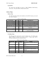
1
Group BCM Advanced Research FM519 External Product Specification April 30, 1997 Revision X0.1 Written By: John Zwaans Revision History FM519 Specification Revision X0.0 X0.1 X0.2 Date 04/30/97 05/12/97 05/19/97 PRELIMINARY Description Preliminary release for internal review. Changes and additions Changes and additions Cyrix is a registered trademark of Cyrix Corporation Copyright © 1996, BCM Advanced Research Preface BCM Advanced Research ii FM519 Specification PRELIMINARY This document specifies the architecture for a Cyrix™ Processor based MultiMedia motherboard; The “FM519” is a High-volume Integrated desktop motherboard incorporating advanced Graphics and a sound subsystem. The system incorporates the recommended functionality to support Windows ‘95. Features Processor/Cache Processor System Memory Memory Size Cyrix GX86 Single Chip Computer. 30/120, 33/133, 30/150 Operation Memory Sites SIMM Type Access Time 8 MB minimum to 128 MB maximum. With Single and Double sided SIMM’s. EDO DRAM 4x72 pin SIMM Sockets 4, 8, 16, 32, 64 with Parity and Non-parity (x32 or x36) 60ns EDO or faster Chipset Cyrix 5510 PCI/ISA Chipset. Integrated Graphics Graphics Controller Integrated PCI Graphics & Video Accelerator. Video Memory Shared Frame Buffer in Main Memory Organization 1MB to 2MB TV Output TV Output using Chrontel CH7002 Integrated I/O I/O Controller Serial Ports SMC FDC37C935 (Plug & Play Compliant) Two Asynch serial ports, two 9 Pin connectors using High Speed 16C550 compatible ports with 16-byte FIFOs Infrared Interface One 6 pin infrared port with IrDA and ASKIR Parallel Port One 25 pin supporting EPP, ECP and Centronics Interface Hard Disk Controller PCI Bus Mastering IDE. Native and Compatible Mode Support. IDE Transfer with Scatter Gather. Multiword DMA Transfers Mode 0,1,2. Enhanced IDE PIO Mode 3&4 Hard Disk Connector 2 PCI IDE Connectors for 4 Drives Support Floppy Controller 1.2, 1.44 and 2.88 MB support Keyboard Port PS/2 (Integrated in the FDC37C935) Mouse Port PS/2 (Integrated in the FDC37C935) Real Time Clock Integrated in the FDC37C935 (DS1287 Compatible) Integrated Sound Sound Chip CODEC BCM Advanced Research Sound Blaster compatible sound Analog Devices AD1874DAC, 16-bit Stereo iii FM519 Specification FM Synthesis System BIOS BIOS Type Hard Disk Driver Plug&Play Support Special Features PRELIMINARY Built-in (OPL3 compatible) Phoenix Technologies (Phoenix BIOS ’95) 2MB Flash BIOS. Award BIOS also available IDE, Auto-configuring Steerable DMA Channels and Interrupts. ISA Plug&Play Windows 95 ready. Multi-Boot. PCI add-in card autoconfiguration. Power Management Green Features APM1.2. Meets EPA Mod 2.0 (SMI, Stop Clock, HDD, and Monitor Shutdown) Jumpers and Front Panel Connectors Connectors Reset Switch. Green (Suspend/Resume) Button, Green LED, PC Speaker. HD LED. IRDA. IR Remote. Jumpers Password/CMOS Clear. BIOS Recovery. NTSC/PAL TV Out selection Headers and Rear Panel Connectors Headers Floppy. IDE 1&2. Serial 2 Port. Game Port. CD-IN. Modem In Connectors VGA Port. Serial 1. Keyboard & Mouse. Parallel Port. TV Out. Mic In. Line Out. Mechanical Board Style Board Size/Type LPX form factor 9.0” x 8.0”, four layer board Expansion Slots Description One EISA riser slot for ISA and PCI buses BCM Advanced Research iv FM519 Specification PRELIMINARY Document Structure and Outline The information contained in this document is organized into 5 sections. Each section is of a modular format with non-numbered headings for each major topic and sub-topics. First level headings (16 point Times New Roman) always appear at the top of a new page and indicate the beginnings of a new major topic. Pages are numbered by chapter and page (e.g. 1-1). Figures and tables are numbered by chapter and sequence within the chapter. The modular format allows for easy update of the documents as new information becomes available, or as specifications change. Some pages may contain more blank spaces than others; this is done to confine major topics to page boundaries. References from one section to topics in another are by section title rather than number. This is done to maintain modularity. For example, a reference to a topic in Section 3 would be as follows: Refer to “Topic Heading” in the “Functional Architecture” section. The content of each section is summarized below: Section 1: Introduction Provide an overview of the FM519 motherboard showing functional blocks. Section 2: Functional Architecture Describes the way each functional block of the FM519 motherboard works. Summarizes major bus interface signal pin names and their meaning. Their mnemonics appear throughout this document. Section 3: Configuration The FM519 configuration tables with considerations for all the different environments the hardware can be set to is given. Section 4: Operating Environments Describes the Software and Operating System environment. The current Performance benchmarks are listed. Section 5: Electrical, Environmental and Mechanical Specifications Specifies electrical and operational parameters, considerations and other hardware specifications. BCM Advanced Research v FM519 Specification PRELIMINARY References The Following documents should be available for reference when using this document: Order of Preference In the event of conflict between the requirements set forth in this document and the documents herein, the requirements of this document shall prevail. The order of precedence shall be: 1) FM519 Specification (this document) 2) Referenced BCM internal documents 3) Referenced external documents Referenced BCM Internal Documents Several documents are required during the process of design, regulatory approvals, manufacturing and servicing the FM519 product family. The required documents are as follows: • • • • • • • • FM519 PWB Fabrication Drawing FM519 PWB Layout Artwork for each revision of PWB FM519 PWB Gerber Files FM519 Schematics for each revision of PWB & PWA FM519 Assembly Drawings and Process Instructions All production level ECOs Bill of Material (BOM) with Approved Vendor List (AVL) Configuration Jumper combinations Referenced External Documents • • • • • • PCI System Design Guide. Revision 1.0 IBM AT Technical Reference Manual Cyrix GX86 Processor User’s Manual and Data Sheet Cyrix 5510 External Design Specification AD AD1874DAC Data Book SMC FDC37C935 Data Sheet BCM Advanced Research vi FM519 Specification PRELIMINARY TABLE OF CONTENTS Section 1: Introduction Overview..............................................................................................................1-2 Processor Subsystem................................................................................1-2 Cache and Memory Subsystem................................................................1-2 PCI I/O Bus..............................................................................................1-3 Embedded PCI Devices ...........................................................................1-3 PCI Video/Graphics Controller................................................................1-3 TV Output ................................................................................................1-3 PCI Bus Master IDE ................................................................................1-3 PCI Add-in Cards.....................................................................................1-3 Sound Subsystem .....................................................................................1-4 Embedded I/O Subsystem........................................................................1-4 Section 2: Functional Architecture Processor Subsystem............................................................................................2-1 Memory Subsystem .............................................................................................2-1 DRAM Subsystem ...................................................................................2-1 DRAM (SIMM) Sockets..........................................................................2-1 System BIOS............................................................................................2-2 Address Maps.......................................................................................................2-2 Memory Map ...........................................................................................2-2 I/O Address Map......................................................................................2-3 Interrupt Allocation..................................................................................2-4 DMA Channels ........................................................................................2-5 Video Subsystem .................................................................................................2-6 Gx86 Integrated Functions.......................................................................2-6 Graphics Accelerator ...............................................................................2-6 Display Controller....................................................................................2-6 Video DAC ..............................................................................................2-7 Video (Monitor) Connector .....................................................................2-8 TV Output ................................................................................................2-8 TV Output Connectors.............................................................................2-10 Sound Subsystem .................................................................................................2-10 GAME Port Header..................................................................................2-11 Line Out Connector..................................................................................2-12 Line Out Header.......................................................................................2-12 Microphone In Connector ........................................................................2-12 Microphone In Header .............................................................................2-12 ISA/PCI I/O Riser Card .......................................................................................2-13 ISA Interface............................................................................................2-13 AT Bus Refresh........................................................................................2-13 PCI Interface ............................................................................................2-13 ISA/PCI I/O Riser Connector ..................................................................2-14 Storage Subsystem ...............................................................................................2-17 BCM Advanced Research vii FM519 Specification PRELIMINARY IDE Hard Disk Drive Interface ................................................................2-17 Floppy Disk Drive Interface ....................................................................2-18 I/O Subsystem......................................................................................................2-19 Serial Ports ...............................................................................................2-19 Parallel port..............................................................................................2-20 Keyboard Interface...................................................................................2-21 Mouse Interface .......................................................................................2-22 Real-time Clock .......................................................................................2-22 Nonvolatile CMOS Memory Battery.......................................................2-23 IR (Infra-red) Support ..............................................................................2-23 IRDA connector .......................................................................................2-23 Miscellaneous Connectors ...................................................................................2-24 PC Speaker Connector .............................................................................2-24 Modem In Connector ...............................................................................2-24 Hard Drive LED Connector .....................................................................2-25 Suspend/Resume Connector ....................................................................2-25 Reset Connector .......................................................................................2-25 CPU Fan Connector .................................................................................2-26 Power On Connector................................................................................2-26 Section 3: Configuration Product Configuration..........................................................................................3-1 DRAM Subsystem Configurations ..........................................................3-1 Section 4: Operating Environments Software ...............................................................................................................4-1 General.....................................................................................................4-1 BIOS Setup ..........................................................................................................4-1 The Main Menu........................................................................................4-2 Standard CMOS Setup.............................................................................4-3 BIOS Features Setup................................................................................4-5 Power Management Setup .......................................................................4-7 Load BIOS Defaults.................................................................................4-8 Integrated Peripherals ..............................................................................4-9 Supervisor Password................................................................................4-11 User Password..........................................................................................4-11 Save & Exit Setup....................................................................................4-11 Operating Systems ...............................................................................................4-13 Performance .........................................................................................................4-14 Compatibility .......................................................................................................4-16 Section 5: Electrical, Environmental and Mechanical Specification Absolute Maximum Ratings ................................................................................5-1 Electrical ..............................................................................................................5-2 DC Specifications for 5V and 3.6V Signals ............................................5-2 Power Supply .......................................................................................................5-3 Power Supply Connectors........................................................................5-3 BCM Advanced Research viii FM519 Specification PRELIMINARY Input Power Budget .................................................................................5-3 Environmental......................................................................................................5-4 Reliability Specification.......................................................................................5-5 Mechanical...........................................................................................................5-5 Systems Interfaces ...............................................................................................5-5 User-Accessible Sockets..........................................................................5-5 User-accessible Connectors .....................................................................5-5 Back-Panel Interfaces ..........................................................................................5-6 Manufacturability/Serviceability .........................................................................5-7 Regulatory............................................................................................................5-8 Appendix A: PWA Layout...................................................................................5-10 BCM Advanced Research ix FM519 Specification PRELIMINARY Figures Figure 1.1. FM519 Motherboard Block Diagram................................................1-1 Figure 4.1. BIOS Setup Main Menu ....................................................................4-1 Figure 4.1.1.Standard CMOS Setup Menu ..........................................................4-4 Figure 4.1.2. BIOS Features Setup Menu ............................................................4-6 Figure 4.1.3. Power Management Setup Menu....................................................4-8 Figure 4.1.4. Integrated Peripherals Menu...........................................................4-10 BCM Advanced Research x FM519 Specification PRELIMINARY Tables Table 2.1. DRAM memory configurations in Megabytes. ..................................2-1 Table 2.2. DRAM SIMM Pinout Description......................................................2-2 Table 2.3. Memory Map ......................................................................................2-3 Table 2.4. I/O Address Map.................................................................................2-3 Table 2.5. Interrupts Allocation ...........................................................................2-5 Table 2.6. DMA Channels Allocation .................................................................2-5 Table 2.7. Video Monitor Connector Pinout .......................................................2-8 Table 2.8. RCA Jack Connector Pinout ...............................................................2-10 Table 2.9. Y/C Video Connector Pinout..............................................................2-10 Table 2.10. GAME Port Header Pinout ...............................................................2-11 Table 2.11. ISA/PCI I/O Reser Connector Pinout ...............................................2-14 Table 2.12. IDE Connector Pinout.......................................................................2-17 Table 2.13. Floppy Connector Pinout ..................................................................2-18 Table 2.14. Serial Port Connector Pinout. ...........................................................2-20 Table 2.15. Printer Port Connector Pinout...........................................................2-20 Table 2.16. Keyboard Connector Pinout..............................................................2-21 Table 2.17. Mouse Connector Pinout ..................................................................2-22 Table 2.18. Infrared “IrDA” Connector Pinout ...................................................2-23 Table 2.19. PC Speaker Connector Pinout...........................................................2-24 Table 2.20. Modem In Connector Pinout.............................................................2-24 Table 2.21. Hard Drive LED Header Pinout........................................................2-25 Table 2.22. Suspend/Resume Connector Pinout..................................................2-25 Table 2.23. Reset Connector Pinout ....................................................................2-25 Table 2.24. CPU Fan Connector Pinout...............................................................2-26 Table 2.25. Power On LED Connector Pinout ....................................................2-27 Table 3.1. SIMMs Configurations .......................................................................3-1 Table 4.1. Main Menu Selections ........................................................................4-3 Table 4.1.1. Standard CMOS Setup.....................................................................4-5 Table 4.1.2. BIOS Features Setup........................................................................4-7 Table 4.1.3. Power Menu Selections ...................................................................4-9 Table 4.1.4. Integrated Peripherals Selections.....................................................4-11 Table 5.1. Absolute Maximum Ratings ...............................................................5-1 Table 5.2. 5 Volt DC Specifications ....................................................................5-2 Table 5.3. 3.6 Volt DC Specifications .................................................................5-2 Table 5.4. Power Supply Connector ....................................................................5-3 Table 5.5. FM519 Motherboard Power Budget ...................................................5-4 Table 5.6. Environmental Specifications .............................................................5-4 Table 5.7. Motherboard MTBF............................................................................5-5 Table 5.8. Accessible Sockets..............................................................................5-5 Table 5.9. Accessible Connectors........................................................................5-5 Table 5.10. Back-Panel Interfaces .......................................................................5-6 BCM Advanced Research xi FM519 Specification PRELIMINARY 1 Introduction This section provides an overview for a Cyrix 6x86 based PCI/ISA Printed Wiring Assembly (PWA), code named "FM519". It describes functional blocks and their relationship. The following diagram shows the functional blocks of the FM519. Figure 1-1. FM519 Motherboard Block Diagram Clock Gen SIMM SOUND CODEC VGA CONN. VGA RAMDAC Media GX System Controller GX86 TV OUT CONN. ENCODER PCI IDE Bus Master GX 5510 GAME PORT Primary IDE Connector Secondary IDE Connector Address ISA Bus Data FLASH BIOS K/B SMC Ultra I/O 37C93X PRINT FDD RTC DS1287 PS/2 MOUSE IRDA CON. IR BCM Advanced Research Y/C Video RCA Jack PCI Bus Address/Data PHONO JACK Crystal 1-1 RTC COM 1 / COM 2 EISA SLOT FM519 Specification PRELIMINARY Overview The FM519 is an implementation of BCM Advanced Research for a HighVolume motherboard featuring these subsystems: • • • • • • • • • Cyrix GX86 Single Chip Processor Cyrix 5510 Chipset One EISA Riser Card Sound Blaster Pro compatible sound Wavetable upgrade socket Integrated PCI Graphics/Video Accelerator PCI IDE Bus Master interface Embedded advanced I/O support LPX form-factor motherboard The target Operating Systems for the FM519 are: DOS/Windows, Windows 95, Windows NT, OS/2 and UNIX. Processor Subsystem The FM519 has the Cyrix® Gx86 Processor soldered on the motherboard. The Cyrix® Gx86 Processor is an integrated 64-bit x86-compatible microprocessor. The integration includes a high-performance 2D graphics subsystem, an integrated PCI interface, and a unified memory subsystem. Enhancements to the SMM architecture enable Cyrix’s Virtual System Architecture (VSA) for Virtual VGA and Virtual Audio. Cyrix’s Display Compression Technology eliminates the performance degradation associated with traditional UMA system designs. Cache and Memory Subsystem The cache and main memory DRAM control functions are part of the Cyrix® Gx86 Processor. The 16-KByte internal write-back unified cache is a data/instruction cache and is configured as four-way set associative. The cache stores up to 16 KBytes of code and data in 1024 cache lines. The Gx86 provides the ability to allocate a portion of the L1 Cache as a scratchpad which is used to accelerate the Virtual Systems Architecture algorithms as well as for some graphics operations. The FM519 provides no second level cache. Main Memory is provided through four (4) 72-pin SIMM socket sites supporting either single or double-sided DRAM modules in a 64-bit wide two bank arrangement. The FM519 can support up to 128MB (2 Banks) of DRAM. Each bank can be single or double sided EDO (Extended Data Out) DRAM. The BCM Advanced Research 1-2 FM519 Specification PRELIMINARY installed DRAM type can be 4MB, 8MB, 16MB, 32MB or 64MB SIMMs, and both Symmetrical or Asymmetrical DRAM technology are supported. When only one bank of SIMMs is used it must be installed in Bank 0. PCI I/O Bus The primary I/O bus for the FM519 is PCI. It supports up to three masters on the PCI bus. The PCI bus operates at 33 MHz. Embedded PCI Devices The PCI bus contains 2 embedded PCI devices: PCI IDE interface and PCI Video/Graphics controller using the Gx86 processor’s internal video interface. Arbitration for the PCI bus is performed by the Gx86 PCI GX Arbiter. PCI Video/Graphics Controller A high-performance graphics Accelerator is integrated into the Cyrix Gx86 Processor. Video memory is shared with system memory, however by using Cyrix’s Display Compression Technology (DCT), the performance degradation inherent in traditional UMA systems is eliminated. An external video RAM-DAC provides the output for the monitor. TV Output A Chrontel CH7002 chip provides video output for a TV. Both RCA and a SVideo connectors are provided for this purpose. PCI Bus Master IDE The Cyrix Cx5510 chip provides two integrated IDE controllers with two high performance IDE interfaces for up to four devices, such as Hard Drives and CDROM. BCM Advanced Research 1-3 FM519 Specification PRELIMINARY PCI Add-in Cards High Performance PCI I/O cards can be used in the FM519 through the expansion connectors in the riser card. The PCI bus is specified to support 10 loads. Each embedded controller or bridge (Video, PCI to ISA bridge) count as 1 load, each PCI expansion slot used in the riser card count as 1.5 loads (the connector to the riser card count as 1.5 loads). Sound Subsystem The Sound Section is intended to provide an integrated audio solution for business audio, education, entertainment sound, games and multimedia applications. Full compatibility with all of the De-facto standards is provided. The FM519 incorporates all of the functions and interfaces for compatibility with the Sound Blaster card.. Embedded I/O Subsystem The SMC (Standard Microsystems Corp.) Plug and Play Ultra I/O controller “FDC37C935” represents the newest technology in functionality and integration. While providing the standard PC I/O requirements the Ultra I/O complies with the ISA Plug-and-Play standard version 1.0a, and provides for the recommended functionality to support Windows ‘95. The Ultra I/O qualifies 16-bit address to allow relocation of 480 different addresses, with 13 IRQ options and 3 DMA channels available for each logical device. Other features of the Ultra I/O are: 8042 keyboard controller. Real Time Clock. An Infrared interface for IrDA and ASKIR. Floppy interface. Two serial ports with 16-byte FIFOs. One EPP/ECP supported bi-directional parallel port. BCM Advanced Research 1-4 FM519 Specification PRELIMINARY 2 Functional Architecture Processor Subsystem The Cyrix Gx86 processor that is used on the FM519 motherboard is soldered directly on the FM519 Motherboard and runs at either 30/120, 33/133 MHz or 30/150 MHz. A large heat sink is glued on the processor to eliminate the danger of over- heating. Memory Subsystem DRAM Subsystem The FM519 supports four 36-bit (72-pin) SIMM sockets (SIMM1, SIMM2, SIMM3, SIMM4), allowing system memory from 8 MB to 128 MB of main DRAM. Population must be done in pairs of SIMMs of the same memory type. There are no jumpers settings required for the memory size or type, which is automatically detected by the system BIOS. The SIMM sockets have tin-lead contacts, rather than the more expensive gold contacts. The SIMMs are rated at 60ns or better. Only EDO (Extended Data Out) SIMMs are supported. When only one bank is used the EDO SIMMs must be placed in bank 0 (SIMM1 and SIMM2). All the allowable memory size configurations are described on table 2.1 (Refer to Table 3.2 in the “Configuration” section for the different combinations and sizes of SIMMs). Table 2.1. DRAM memory configurations in Megabytes. 8 16 24 32 40 48 64 72 80 96 128 DRAM (SIMM) Sockets Connection to the main system DRAM is via four (4) connectors on the system PWA. Reference: Connector Type: Connector Part Number: BCM Advanced Research SIMM1, SIMM2, SIMM3, SIMM4 female, 72 pin SIMM, in-line connector AMP 822110-3 or equivalent 2-1 FM519 Specification PIN 1 2 3 4 5 6 7 8 9 10 11 12 13 14 15 16 17 18 19 20 21 22 23 24 25 26 27 28 29 30 31 32 33 34 35 36 PRELIMINARY Table 2.2. DRAM SIMM Pinout Description DESCRIPTION PIN DESCRIPTION SIGNAL-GROUND 37 PARITY DATA 1 DATA 0 38 PARITY DATA 3 DATA 16 39 SIGNAL-GROUND DATA 1 40 CAS 0* DATA 17 41 CAS 2* DATA 2 42 CAS 3* DATA 18 43 CAS 1* DATA 3 44 RAS 0* DATA 19 45 RAS 1* VCC 46 N/C N/C 47 WRITE-ENABLE* ADDRESS 0 48 N/C ADDRESS 1 49 DATA 8 ADDRESS 2 50 DATA 24 ADDRESS 3 51 DATA 9 ADDRESS 4 52 DATA 25 ADDRESS 5 53 DATA 10 ADDRESS 6 54 DATA 26 ADDRESS 10 55 DATA 11 DATA 4 56 DATA 27 DATA 20 57 DATA 12 DATA 5 58 DATA 28 DATA21 59 VCC DATA 6 60 DATA 29 DATA 22 61 DATA 13 DATA 7 62 DATA 30 DATA 23 63 DATA 14 ADDRESS 7 64 DATA 31 N/C 65 DATA 15 VCC 66 N/C ADDRESS 8 67 N/C ADDRESS 9 68 N/C RAS 3* 69 N/C RAS 2* 70 N/C PARITY DATA 2 71 N/C PARITY DATA 0 72 LOGIC-GROUND BCM Advanced Research 2-2 FM519 Specification PRELIMINARY System BIOS The system and video BIOS are stored in a 2MB (256KBx8) Flash Memory device (U4). The system BIOS is shadowed and cached. Address Maps Memory Map The following table describes the breakdown of the FM519 memory areas and how they are assigned. Table 2.3. Memory Map SIZE TO DESCRIPTION 128KB 4GB BIOS ROM 1MB 16MB Optional memory space gap 64KB 1MB System BIOS (Shadowed in DRAM) 160KB 960KB Expansion region (Shadowed in DRAM) 32KB 800KB Video BIOS (Shadowed in DRAM) 128KB 768KB Video Buffer (SMM space NonCacheable) 128KB 640KB Optional memory space gap (DOS Apps) 512KB 512KB DOS applications (No read/write protect) (Always cacheable) LOCATION FFF80000-FFFFFFFF 00F00000-00FFFFFF 000F0000-000FFFFF 000C8000-000EFFFF 000C0000-000C7FFF 000A0000-000BFFFF 00080000-0009FFFF 00000000-0007FFFF I/O Address Map The following table represents the system I/O address map. I/O address range 000H to 0FFH are reserved for the system board I/O. Address range 100h to 3FFH are available to the I/O on-board resources. HEX-RANGE 0060 0064 0070-007F 00E0-00EF 00F0 00F1 0F8-0FF Table 2.4. I/O Address Map SIZE Plug&Play USAGE 1 byte N/A KEYBOARD CONTROLLER DATA BYTE 1 byte N/A KEYBOARD CONT. CMD/STATUS BYTE 16 bytes N/A REAL-TIME CLOCK, NMI MASK 16 bytes N/A RESERVED 1 byte N/A CLEAR MATH COPROCESSOR ERROR 1 byte N/A RESET MATH COPROCESSOR 8 bytes N/A MATH COPROCESSOR BCM Advanced Research 2-3 FM519 Specification PRELIMINARY 200,202,207 3 bytes 220-22F 17 bytes 238-23F 8 bytes 278-27F 2B0-2DF 2F8-2FF 338-33F 8 bytes 48 bytes 8 bytes 8 bytes YES 370-375 6 bytes YES 376 1 byte NO 377 1 byte NO 378-37F 3B0-3BF 8 bytes 16 bytes YES 3C0-3CF 3D0-3DF 3F0-3F5, 3F7 16 bytes 16 bytes 7 bytes YES 3F8-3FF CF8-CFF 8 bytes 8 bytes YES N/A BCM Advanced Research YES (Rev 1.1) YES (Rev 1.1) YES YES YES 2-4 GAME I/O SOUND PORT SERIAL PORT 4 (USED FOR REMAPPING ) PARALLEL PORT 2 ALTERNATE EGA ADAPTER SERIAL PORT 2 SERIAL PORT 3 (USED FOR REMAPPING) FLOPPY CONT. (SECONDARY ADDRESS) SECONDARY IDE CHANNEL CMD PORT SECONDARY IDE CHANNEL STAT PORT PARALLEL PORT 1 MONO DISPLAY & PRINTER ADAPTER EGA ADAPTER CGA ADAPTER FLOPPY CONTROLLER (PRIMARY) SERIAL PORT 1 PCI CONFIGURATION SPACE FM519 Specification PRELIMINARY Interrupt Allocation INTERRUPT IRQ0 IRQ1 IRQ2 IRQ3 IRQ4 IRQ5 IRQ6 IRQ7 IRQ8 IRQ9 IRQ10 IRQ11 IRQ12 IRQ13 IRQ14 IRQ15 Table 25. Interrupts Allocation Plug&Play DESCRIPTION N/A TIMER YES KEYBOARD CONTROLLER N/A IRQ FROM SECOND INTERRUPT CONTROLLER YES COM2 AND COM4 YES COM1 AND COM3 YES SOUND PORT YES FLOPPY DISK CONTROLLER YES PRIMARY LPT N/A REAL-TIME CLOCK YES AVAILABLE AVAILABLE AVAILABLE YES ON-BOARD PS/2 MOUSE N/A MATH COPROCESSOR NO PRIMARY IDE HARD DRIVE NO SECONDARY IDE HARD DRIVE IF PRESENT, ELSE USER AVAILABLE DMA Channels CHANNEL DMA0 DMA1 DMA2 DMA3 DMA4 DMA5 DMA6 DMA7 BCM Advanced Research Table 2.6. DMA Channels Allocation Plug&Play DESCRIPTION YES (Rev ON-BOARD AUDIO (default) 1.1) YES (Rev ON-BOARD AUDIO (default) 1.1) YES FLOPPY DISK CONTROLLER YES PARALLEL PORT IN ECP/EPP MODE N/A 16-BIT DRQ/DACK FROM SECOND DMA CONTROLLER AVAILABLE AVAILABLE AVAILABLE 2-5 FM519 Specification PRELIMINARY Video Subsystem Gx86 Integrated Functions The Cyrix Gx86 Integrated Processor integrates the following functions typically implemented using external devices: • High-performance graphics accelerator • Display Controller for the CRT • EDO memory controller • PCI Bridge • Power management The processor has also been enhanced to support Cyrix’s proprietary Virtual Systems Architecture implementation. The Gx86 Integrated Processor is the first processor to implement a Unified Memory Architecture. By using Cyrix’s Display Compression Technology (DCT), the performance degradation inherent in traditional UMA systems is eliminated. Graphics Accelerator The graphics accelerator is a full-featured GUI accelerator. The graphics pipeline implements a bitBLT engine for frame buffer bitBLTs and rectangular fills. The bitBLT engine also assists the CPU in bitBLTs between system memory and the frame buffer by cooperating with new instructions in the integer core. This combination of hardware and software is used by the display driver to provide very fast transfers in both directions between system memory and the frame buffer. The bitBLT engine also draws randomly-oriented vectors, and scanlines for polygon fill. All of the pipeline operations described in the following list can be applied to any bitBLT operation. • Pattern Memory. Render with 8x8 dither, 8x8 monochrome, or 8x1 color pattern. • Color Expansion. Expand monochrome bitmaps to full-depth 8-bit or 16-bit colors. • Transparency. Suppresses drawing of background pixels for transparent text. • Raster Operations. Boolean operation combines source, destination, and pattern bitmaps. Display Controller The display port interfaces directly to a RAMDAC to drive a CRT display. The display controller retrieves image data from the frame buffer region of memory, performs a color-look-up if required, inserts the cursor overlay into the pixel stream, generates display timing, and formats the pixel data for output to a variety of display devices. The display controller contains Display Compression Technology that allows the Gx86 processor to refresh the display from a compressed copy of BCM Advanced Research 2-6 FM519 Specification PRELIMINARY the frame buffer. DCT typically decreases the screen-refresh bandwidth requirement by a factor of 15 to 20, further minimizing bandwidth contention. Video DAC The ICS5342 GENDAC is a combination of dual programmable clock generators, a 256 x 18-bit RAM, and a triple 8-bit video DAC. The GENDAC supports 8-bit pseudo color applications, as well as 15-bit, 16-bit, and 24-bit True Color bypass for high speed, direct access to the DACs. The RAM makes it possible to display 256 colors selected from a possible 262,144 colors. The dual clock generators use Phase Locked Loop (PLL) technology to provide programmable frequencies for use in the graphics subsystem. The video clock contain 8 frequencies, all of which are programmable by the user. The memory clock has two programmable frequency locations. The three 8-bit DACs on the ICSS342 are capable of driving singly or doubly-terminated 75Ω loads to nominal 0 - 0.7 volts at pixel rates up to 135 MHz. Differential and integral linearity errors are less than 1 LSB over full temperature and VDD ranges. Monotonicity is guaranteed by design. On-chip pixel mask register allows displayed colors to be changed in a single write cycle rather than by modifying the color palette. Features • • • • • • • • • • • • • Triple video DAC, dual clock generator, and 16 bit pixel port Dynamic mode switch allows switching color depth on a pixel by pixel basis 24 (packed and sparse), 16, 15, or 8-bit pseudo color pixel mode supports True Color, Hi-Color, and VGAmodes High speed 256x6x3 color palette (135MHz) with bypass mode & 8-bit DACs Eight programmable video (pixel) clock frequencies (CLK0) DAC power down in blanking mode Anti-sparkle circuitry On-chip loop filters reduce external components Standard CPU interface Single external crystal (typically 14.318 MHz) Monitor sense Internal voltage reference Very low clock jitter BCM Advanced Research 2-7 FM519 Specification PRELIMINARY Video (Monitor) Connector Connection to VGA monitor is via a connector on the rear panel on the system PWA. Reference: Connector Type: Connector Part Number: P1 (VGA) female, high density DB15S, 15-pin AT-compatible 3M 927F55-01-15-10 or equivalent Table 2.7. Video Monitor Connector Pinout PIN Description 1 RED 2 GREEN 3 BLUE 4 N/C 5 LOGIC-GROUND 6 RED GROUND RETURN 7 GREEN GROUND RETURN 8 BLUE GROUND RETURN 9 +5V PULL-UP 10 LOGIC GROUND 11 N/C 12 DDC DAT 13 HORIZONTAL-SYNC 14 VERTICAL-SYNC 15 DDC CLK 16 LOGIC-GROUND1 17 LOGIC-GROUND1 1: Pins 16 and 17 are connector mounting holes connected to logic ground. TV Output The TV output is generated by the CH7002 which is a fully integrated system solution for converting analog RGB and synchronization signals from a standard VGA source into high-quality NTSC or PAL video signals. This solution involves both hardware and software elements which work together to produce an optimum TV screen image based oh the original computer generated pixel data. All essential circuitry for this conversion are integrated on chip. On chip circuitry includes memory, memory control, scaling, PLL,ADC, DAC, filters, and NTSC/PAL encoder. All internal signal processing, including NTSC/PAL encoding, is performed using digital techniques to ensure that the high-quality video signals are not affected by drift issues associated with analog components. BCM Advanced Research 2-8 FM519 Specification PRELIMINARY The CH7002 is a complete TV output subsystem which uses both hardware and software element to produce an image on TV which is virtually identical to the image that would be displayed on a monitor. Simply creating a compatible TV output from a VGA input is a relatively straightforward process. This process includes a standard conversion from RGB to YUV color space, converting from a non-interlaced to an interlaced frame sequence, and encoding the pixel stream into NTSC or PAL compliant format. However, creating an optimum computer generated image on a TV screen involves a highly sophisticated process of scaling, deflickering, and filtering. This results in a compatible TV output that displays a sharp and stable image, of the right size with minimal artifacts from the conversion process. As a key part of the overall system solution, the CH7002 software establishes the correct framework for the VGA input signal to enable this process. Once-the display is set to a supported resolution (either 640x480 or 800x600), the CH7002 software may be invoked to establish the appropriate TV output display. The software then programs the various timing parameters of the VGA controller to create an output signal that will be compatible with the chosen resolution, operating mode, and TV format. Adjustments performed in software include pixel clock rates, total pixels per line, and total lines per frame. By performing these adjustments in software, the CH7002 can render a superior TV image without the added cost of a full frame buffer memory normally used to implement features such as scaling and full synchronization. Without this added system software, TV output solutions can only guarantee compatible operation in VGA standard mode 12 (640x480x16 color, 60 Hz). The CH7002 hardware accepts direct VGA output (analog RGB inputs), which is digitized on a pixel-by-pixel basis by three 8-bit video A/D converters. The digitized RGB inputs are then color space converted into YUV in 4-2-2 format (encoded into luminance (Y) and color-difference (U,V) signals and stored in a line buffer memory. The stored pixels are fed into a block where scan-rate conversion, underscan scaling and 3-line vertical flicker filtering are performed. The scan-rate converter transforms the VGA horizontal scan-rate to either NTSC or PAL scan-rates, the vertical flicker filter eliminates flicker at the output while the underscan scaling reduces the size of the displayed image to fit onto a TV screen. The resulting YW signals are filtered through digital filters to minimize aliasing problems. The digital encoder receives the filtered signals and transforms them to composite and S-video outputs, which are converted by the three 8-bit DACs into analog outputs. BCM Advanced Research 2-9 FM519 Specification PRELIMINARY TV Output Connectors Two connectors are provided to connect a TV to the board. Reference: Connector Type: Connector Part Number: (RCA JACK) TBD TBD Table 2.8. RCA Jack Connector Pinout PIN 1 2 3 4 Reference: Connector Type: Connector Part Number: SIGNAL Composite Video GROUND GROUND GROUND J2 (Y/C Video) TBD TBD Table 2.9. Y/C Video Connector Pinout PIN 1 2 3 4 5 6 7 BCM Advanced Research SIGNAL GROUND GROUND LUMA CHROMA GROUND GROUND GROUND 2-10 FM519 Specification PRELIMINARY Sound Subsystem The Cx5510 System controller incorporates features of the Virtual System Architecture (VSA) for the generation and capture of audio using an external DAC or Codec. Virtual Audio is compatible with software written for the Sound Blaster II, Pro, and 16, and the Adlib audio cards. Virtual Audio also emulates an MPU-401 UART using a COM port for MIDI serial transmit and receive. The Cx5510 Virtual Audio hardware includes two 128-byte audio FIFOs to hold 32 audio samples (two channels at 16 bits per channel) for buffering digitized audio input and output from/to the external DAC or Codec. The audio FIFOs provide communication between the internal parallel bus and an external serial DAC or Codec. The Cx5510 also contains a full set of configuration audio registers and hardware comparators for trapping and signalling I/O accesses to the audio address range. Cyrix Virtual Audio software emulates audio functions that are trapped by the Cx5510. This software is available to OEMs for incorporation into the system BIOS ROM. The Cx5510 interfaces to the Analog Devices AD1847 Codec for audio playback and record. The VSA Virtual Audio hardware resources in the Cx5510 perform the following functions: • Buffers the input and output with two 128-byte FIFOs, each holding 32 32-bit samples (the 32-bit sample is 16 bits per stereo channel). One FIFO is for audio input and one FIFO is for audio output. • For audio input/output, it interfaces with AD1847 Serial Port Codec. • Generates an SMI to alert software of required data update. SMI is generated when either FIFO drops below separately programmable thresholds, or when output FIFO is empty or input FIFO is full. Also generates an SMI on I/O traps. • Traps I/O accesses for Sound Blaster compatibility at either 220h-22Fh, 240h24Fh, 260h-26Fh, or 280h-28Fh. • Traps I/O accesses for ADLIB compatibility at 388h-38Bh. • Traps I/O accesses for Roland MPU 401UART interface at 300h-301h or 330h331h. • Traps I/O accesses for MIDI serial input and output at COM2 (2F8h-2FFh) or COM4 (2E8h-2EFh). • Supports I/O trapping for low (00h-0Fh) and/or high (C0h-DFh) DMA accesses. • Supports hardware status register reads in Cx5510, minimizing SMI overhead. • Generates IRQs for SB DSP chip compatibility: support for software-generated IRQs on IRQ 2, 3, 5, 7, 10, 11, 12, 13,14, and 15. GAME Port Header The FM519 provides access to the Joystick game compatible interface through a header in the system PWA. Reference: Connector Type: BCM Advanced Research HDR1 (GAME) male, 2 x 8, 0.100" centerline, straight 2-11 FM519 Specification Connector Part Number: PIN 1 2 3 4 5 6 7 8 PRELIMINARY AMP 103322-8 or equivalent Table 2.10. MIDI/Game port Connector Pinout DESCRIPTION PIN DESCRIPTION 9 10 11 12 13 14 15 16 Line Out Connector The audio subsystem provides external sound through a user accessible stereo jack connector (J16) soldered to the PWA. This jack will allow the connection of self-amplified speakers. Reference: Connector Type: Connector Part Number: J14 (LINE OUT) 1/8 in. Banana Jack Connector Vendor 10XXXX-2 Line Out Header The audio subsystem also provides external sound through a header (J15) soldered to the PWA. This header will allow a jack on the front panel of the enclosure to be connected via a cable. Reference: Connector Type: Connector Part Number: J15 1X3 male straight, .100 centers AMP 103321-3 or equivalent Microphone In Connector An external accessible jack connector (J14) is soldered to the PWA to allow the connection of a microphone for voice input. Reference: Connector Type: Connector Part Number: BCM Advanced Research J12 (MIC IN) 1/8 in. Banana Jack Connector Vendor 10XXXX-2 2-12 FM519 Specification PRELIMINARY Microphone In Header The audio subsystem also provides a microphone input through a header (J13) soldered to the PWA. This header will allow a jack on the front panel of the enclosure to be connected via a cable. Reference: Connector Type: Connector Part Number: J13 1X3 male straight, .100 centers AMP 103321-3 or equivalent ISA/PCI I/O Riser Card The FM519 system will support an ISA only, PCI only or shared ISA-PCI slots riser card. The ISA/PCI I/O riser card contains decoupling capacitors between the voltage planes and ground to assist in both EMI and general voltage plane noise reduction. The ISA/PCI I/O riser will be inserted into the system PWA during the system assembly process. The riser connects to the system PWA through the J10 connector. ISA Interface The FM519 incorporates a fully ISA bus compatible master and slave interface. It is capable of driving five (5) ISA Slots without external data buffers. This drive capability is required to ensure signal integrity for the ISA bus under loading conditions with the ISA/PCI I/O riser and expansion cards installed. The ISA interface also provides byte swap logic and I/O recovery support. AT Bus Refresh The Cx5510 supports the standard ISA refresh function. ISA refreshes are enabled by setting bit 6 in the ISA Configuration Register. When enabled, Timer 1 in the programmable interval timer is used to generate an internal refresh request signal. When the ISA bus is not in use by the ISA bus controller, the DMA controller, or an ISA bus master, the refresh control logic generates the ISA refresh cycle. No DMA or PCI-to-ISA cycles occur until after the completion of this refresh cycle. If the ISA bus is in use when the refresh request occurs, the refresh controller waits until the bus is free and then generate a refresh cycle. The Cx5510 also supports refresh requests initiated by ISA masters. PCI Interface The Gx86 CPU includes an integrated PCI controller with the following features. BCM Advanced Research 2-13 FM519 Specification PRELIMINARY X-bus PCI Slave • 16-byte PCI write buffer • 16-byte PCI read buffer from X-bus • Synchronization of 1x, 2x, 3x, 4x, 5x PCI to X-bus • Supports cache line bursting • Write/Inv line support • Pacing of data for read or write operations with X-bus • No active byte enable transfers supported X-bus PCI Master • 16 byte X-bus to PCI write buffer • Synchronization of 1x, 2x, 3x, 4x, 5x X-bus to PCI • Configuration read/write Support • Int Acknowledge support • Lock conversion • Support fast back-to-back cycles as slave PCI Arbiter • Fixed, rotating, hybrid, or ping-pong arbitration (programmable) • Support four masters, three on PCI • Internal REQ for CPU • Master retry mask counter • Master dead timer. • Resource or total system lock support ISA/PCI I/O Riser Connector Connection to the PCI/ISA riser is via a connector on the system PWA. Reference: Connector Type: Connector Part Number: PIN B1 B2 B3 B4 B5 B6 B7 B8 B9 J10 female, 198 pin edge connector AMP 646039-1 or equivalent Table 2.11. PCI/ISA Riser Connector SIGNAL NAME PIN SIGNAL NAME GND A1 IOCHK* RSTDRV A2 SD7 VCC A3 SD6 IRQ9 A4 SD5 -5VDC A5 SD4 DRQ2 A6 SD3 -12VDC A7 SD2 OWS* A8 SD1 +12VDC A9 SD0 BCM Advanced Research 2-14 FM519 Specification B10 B11 B12 B13 B14 B15 B16 B17 B18 B19 B20 B21 B22 B23 B24 B25 B26 B27 B28 B29 B30 B31 D1 D2 D3 D4 D5 D6 D7 D8 D9 D10 D11 D12 D13 D14 D15 D16 D17 D18 F1 F2 F3 F4 PRELIMINARY GND SMEMW SMEMR IOW IOR DACK3 DRQ3 DACK1 DRQ1 REFRESH SYSCLK IRQ7 IRQ6 IRQ5 IRQ4 IRQ3 DACK2 TC BALE VCC OSC GND MEMCS16 IQCS16 IRQ10 IRQ11 IRQ12 IRQ13 IRQ14 DACK0DRQ0 DACK5 DRQ5 DACK6 DRQ6 DACK7 DRQ7 +VCC MASTER GND GND GND PCI INT3 PCI INT4 - BCM Advanced Research A10 A11 A12 A13 A14 A15 A16 A17 A18 A19 A20 A21 A22 A23 A24 A25 A26 A27 A28 A29 A30 A31 C1 C2 C3 C4 C5 C6 C7 C8 C9 C10 C11 C12 C13 C14 C15 C16 C17 C18 E1 E2 E3 E4 2-15 CHRDY AENn SA19 SA18 SA17 SA16 SA15 SA14 SA13 SA12 SA11 SA10 SA9 SA8 SA7 SA6 SA5 SA4 SA3 SA2 SA1 SA0 SBHE LA23 LA22 LA21 LA20 LA19 LA18 LA17 MRDC* MWTC* SD8 SD9 SD10 SD11 SD12 SD13 SD14 SD15 GND GND PCI INT1PCI INT2- FM519 Specification F5 F6 F7 F8 F9 F10 F11 F12 F13 F14 F15 F16 F17 F18 F19 F20 F21 F22 F23 F24 F25 F26 F27 F28 F29 F30 F31 H1 H2 H3 H4 H5 H6 H7 H8 H9 H10 H11 H12 H13 H14 H15 H16 H17 PRELIMINARY VCC KEY VCC PCLKF GND GNT1 GND REQ1 AD31 AD30 N/C KEY N/C AD27 AD26 CBE3 AD23 AD21 AD10 N/C KEY N/C AD17 IRDY DEVSEL PLOCK PERR SERR AD15 AD14 AD12 GND KEY GND AD10 AD8 AD7 AD5 AD3 AD1 AD0 KEY VCC VCC BCM Advanced Research E5 E6 E7 E8 E9 E10 E11 E12 E13 E14 E15 E16 E17 E18 E19 E20 E21 E22 E23 E24 E25 E26 E27 E28 E29 E30 E31 G1 G2 G3 G4 G5 G6 G7 G8 G9 G10 G11 G12 G13 G14 G15 G16 G17 2-16 VCC KEY VCC PCIRSTGNTO REQ0 GND PCIKE GND AD30 N/C KEY N/C AD28 AD28 AD24 AD22 AD20 AD18 N/C KEY N/C AD16 FRAME CBE2 TRDY STOP SDONE SBO CBE1 PAR GND KEY GND AD13 AD11 AD9 CBE0 AD6 AD4 AD2 KEY VCC VCC FM519 Specification H18 H19 PRELIMINARY GND GND G18 G19 GND GND Storage Subsystem IDE Hard Disk Drive Interface The FM519 provides two (2) independent high performance PCI IDE interfaces capable of supporting PIO Mode 3 and Mode 4 devices. The integrated IDE interface can control up to four IDE devices allowing for both CD-ROM and Hard Disk drives. IDE PRI & IDE SEC are the primary and secondary IDE connectors. Both IDE controllers can be disabled through BIOS to allow for external disk drive controllers. Connection to the IDE hard disks is via headers on the system PWA. Reference: Connector Type: Connector Part Number: J6, J4 (PRIMARY, SECONDARY) male, 2 x 20, 0.100" centerline, straight AMP 2-103322-0 Table 2.12. IDE Connector Pinout PIN DESCRIPTION PIN DESCRIPTION 1 RESET* 2 LOGIC-GROUND 3 HD7 4 HD8 5 HD6 6 HD9 7 HD5 8 HD10 9 HD4 10 HD11 11 HD3 12 HD12 13 HD2 14 HD13 15 HD1 16 HD14 17 HD0 18 HD15 19 LOGIC-GROUND 20 N/C1 21 N/C 22 LOGIC-GROUND 23 I/O-WRITE 24 LOGIC-GROUND 25 I/O-READ 26 LOGIC-GROUND 27 HDCHRDY 28 LOGIC-GROUND 29 N/C 30 LOGIC-GROUND 31 IRQ 32 N/C 33 ADDRESS1 34 N/C 35 ADDRESS0 36 ADDRESS2 37 CHIP-SELECT0* 38 CHIP-SELECT1* 39 DISK-ACTIVE 40 LOGIC-GROUND 1: Pin 20 is removed as a key pin. BCM Advanced Research 2-17 FM519 Specification PRELIMINARY Floppy Disk Drive Interface The FM519 has an integrated 765B compatible floppy disk controller using the SMC “FDC37C935” component. The FDC sub-section can control two (1.2, 1.44 and 2.88MB) floppy disks or compatible tape drives. The floppy I/O address can be relocated to 480 different locations. 13 IRQ and 3 DMA channel options are available as well. Includes multiple power-down modes for reduced power use. Connection to the floppy drives is via a header on the PWA. The floppy disk interface contains 48mA drivers and Schmitt trigger inputs on the drive interface. Reference: Connector Type: Connector Part Number: J6 (FLOPPY) male, 2 x 17, 0.100" centerline, straight AMP 1-103322-7 or equivalent Table 2.13. Floppy Connector Pinout PIN DESCRIPTION PIN DESCRIPTION 1 LOGIC-GROUND 2 DENSITY-SELECT* 3 N/C 4 N/C 1 5 LOGIC-GROUND 6 N/C 7 LOGIC-GROUND 8 INDEX* 9 LOGIC-GROUND 10 MOTOR0* 11 LOGIC-GROUND 12 DISK-SELECT1* 13 LOGIC-GROUND 14 DISK-SELECT0* 15 LOGIC-GROUND 16 MOTOR1* 17 MEDIA-ID1* 18 DIRECTION 19 LOGIC-GROUND 20 STEP* 21 LOGIC-GROUND 22 WRITE-DATA* 23 LOGIC-GROUND 24 WRITE-ENABLE* 25 LOGIC-GROUND 26 TRACK00* 27 MEDIA-ID0* 28 WRITE-PROTECT* 29 LOGIC-GROUND 30 READ-DATA* 31 LOGIC-GROUND 32 HEAD-SELECT 33 N/C 34 DISK-CHANGE* 1: Pin 5 is removed as a key pin I/O SUBSYSTEM The I/O Subsystem is consists of a single component from SMC (Standard Microsystems Corp.). The FM519 uses the Plug and Play Compatible Ultra I/O Controller “FDC37C935”, this device provides support for the ISA Plug-and-Play version 1.0a and includes the recommended functionality to support Windows ‘95. Through internal configuration registers, each of the FDC37C935’s logical device’s I/O address, DMA channel and IRQ channel may be programmed. There BCM Advanced Research 2-18 FM519 Specification PRELIMINARY are 480 I/O address location options, 13 IRQ options and 3 DMA channel options for each logical device. The Ultra I/O device provides two (2) high speed NS16C550 compatible serial ports with send/receive 16 Byte FIFOs . One IR two pin port. One Multi-Mode Parallel Port with ChiProtect™ and ECP/EPP modes. And a Floppy/Tape Controller supporting up to 2.88MB transfer rates. Serial Ports The FM519 has two (2) NS16C550 AT-compatible serial ports configured as Data Terminal Equipment (DTE). The electrical characteristics are compliant with the EIA-232-D Serial Communications Specifications. The serial ports may be remapped above other installable serial ports or disabled through BIOS. As a minimum the first serial port (COM1) at J7 must be capable of remapping to COM3. The second serial port (COM2) at J8 must be able to be remapped to COM4. The serial ports I/O address can be relocated within 480 different locations. The default address for COM1, COM2, COM3 and COM4 are 3F8H, 338H, 2F8H and 238H respectively. 13 different IRQ options are available to the serial ports. Connectors located on the rear panel of the system PWA are provided for external connection to the serial ports Reference: Connector Type: Connector Part Number: J7 (COM1) male, 9 pin metal shell D-SUB Amp 750529-3 or equivalent Reference: Connector Type: Connector Part Number: J8 (COM2) male, 2x5, 0.100” centerline, straight Amp 1-103322-5 or equivalent BCM Advanced Research 2-19 FM519 Specification PRELIMINARY PIN 1 2 3 4 5 6 7 8 9 10 11 Table 2.14. Serial Port Connector Pinout. DESCRIPTION DATA-CARRIER-DETECT (DCD) RECEIVE-DATA (RXD) TRANSMIT-DATA (TXD) DATA-TERMINAL-READY (DTR) LOGIC-GROUND DATA-SET-READY (DSR) REQUEST-TO-SEND (RTS) CLEAR-TO-SEND (CTS) RING-INDICATOR (RI) SHELL-GROUND1 SHELL-GROUND1 1: Pins 10 and 11 (Shell Ground) are mounting holes connected to the metal connector housing on serial port 2. Not used on serial port 1. Parallel port The system PWA has a single bi-directional parallel port (EPP/ECP compatible). The parallel port is capable of being disabled or remapped to either the secondary LPT address or the tertiary LPT address through BIOS if other parallel ports are installed in the system. The parallel port I/O address can be relocated within 480 different locations. 3 DMA channels options and 13 different IRQ options are available to the parallel port. A connector is located on the rear panel of the system PWA for the external connection to the port. The parallel port interface contains 12mA source output drivers on the drive interface, and incorporates ChipProtect circuitry for protection against damage due to printer Power-On. Reference: Connector Type: Connector Part Number: J11 (PRINTER) female, 25 pin metal shell D-SUB AMP 750096-3 or equivalent Table 2.15. Printer Port Connector Pinout PIN DESCRIPTION 1 STROBE* 2 PD0 3 PD1 4 PD2 5 PD3 6 PD4 7 PD5 BCM Advanced Research 2-20 FM519 Specification PRELIMINARY 8 9 10 11 12 13 14 15 16 17 18 19 20 21 22 23 24 25 26 27 1: PD6 PD7 ACKNOWLEDGE* BUSY PAPER-END (PE) SELECT AUTO-FEED* ERROR* INIT* SELECT -IN* LOGIC-GROUND LOGIC-GROUND LOGIC-GROUND LOGIC-GROUND LOGIC-GROUND LOGIC-GROUND LOGIC-GROUND LOGIC-GROUND SHELL-GROUND1 SHELL-GROUND1 Pins 26 and 27 are connector mounting holes connected to the metal connector housing. Keyboard Interface The system PWA has a PS/2-compatible keyboard interface. The shielded keyboard interface connector has a PS/2-compatible pinout and is located on the rear panel on the system PWA. To meet the requirements for UL compliance the Vcc pin (pin 4) is connected through a fuse prior to connection to the external connector. Reference: Connector Type: Connector Part Number: PIN 1 2 3 4 5 6 7 BCM Advanced Research J2 (KEYBOARD) female, 6 pin metal shield mini-DIN AMP 749231-1 or equivalent Table 2.16. Keyboard Connector Pinout DESCRIPTION KEYBOARD-DATA N/C LOGIC-GROUND KEYBOARD-Vcc KEYBOARD-CLOCK N/C SHELL-GROUND1 2-21 FM519 Specification PRELIMINARY 8 9 1: SHELL-GROUND1 SHELL-GROUND1 Pins 7-9 are connector mounting hole pins connected to the metal connector housing Mouse Interface The system PWA has a PS/2-compatible mouse interface. The shielded mouse port can be disabled through SETUP. A connector, utilizing PS/2 pinouts, is located on the rear panel on the system PWA. To meet the requirements for UL compliance the Vcc pin (pin 4) was connected through a fuse prior to connection to the external connector. Reference: Connector Type: Connector Part Number: J5 (MOUSE) female, 6 pin metal shield mini-DN AMP 749231-1 or equivalent Table 2.17. Mouse Connector Pinout PIN DESCRIPTION 1 MOUSE-DATA 2 N/C 3 LOGIC-GROUND 4 MOUSE-Vcc 5 MOUSE-CLOCK 6 N/C 7 SHELL-GROUND1 8 SHELL-GROUND1 9 SHELL-GROUND1 1: Pins 7-9 are connector mounting hole pins connected to the metal connector housing. Real-Time Clock The integrated Real Time Clock (RTC) is DS12887/MC146818 compatible and provides the time of day clock, 100-year calendar with alarm features and is accurate to within 1 minute per month, it consumes less than 1 µA of standby current (Typ.). The (RTC) supports 256 bytes of battery backed Non-volatile CMOS memory in two banks of 128 bytes each, both banks being reserved for BIOS use. One bank of CMOS memory is used to maintain the clock and usersystem-setting configuration parameters when the main system power is removed. The other bank (128 bytes) is lockable in 4x32 byte blocks and can be used to store and lock miscellaneous information. BCM Advanced Research 2-22 FM519 Specification PRELIMINARY The CMOS RAM can be set to specific values or cleared to the system default values using the BIOS SETUP program. Also to prevent a lock-up situation the CMOS RAM values can be cleared to the system defaults by using the CLR CMOS jumper on the PWA. Nonvolatile CMOS Memory Battery An external coin-cell style battery provides power to the RTC and CMOS memory when system power is removed. The battery has an estimated lifetime of seven years and is socketed for easy replacement. Reference: Socket Type: BT1 COIN TYPE IR (Infra-Red) Support The FM519 I/O subsystem incorporates an IR interface connector supporting the following industry standards; IrDA (HP-SIR), and ASK-IR. One header J24 (labeled IRDA) provides the interface allowing a two-way wireless communication port using infrared as the transmission medium. The user can transfer files to/from portable devices such as laptops, PDA’s and printers using application software such as LapLink. The IrDA port shares the registers and logic block with COM2 port, once configured in the BIOS for IR a serial device in COM2 will stop transmitting. IRDA Connector A 1 x 6 straight header is available for a cable connection to the IR module. Reference: Connector Type: Connector Part Number: BCM Advanced Research J24 (IRDA) 1 x 6 male straight 0.100 centers AMP 103321-6 2-23 FM519 Specification PRELIMINARY Table 2.18. Infrared “IrDA” Conn. Pinout PIN SIGNAL 1 + 5 VOLTS 2 KEY 3 IR-RX 4 LOGIC-GROUND 5 IR-TX 6 CIR_RX MISCELLANEOUS CONNECTORS PC Speaker Connector A 1 x 4 straight header (J18) is available to drive a chassis-mounted speaker if desired. Reference: Connector Type: Connector Part Number: J18 (SPEAKER) 1 x 4 male straight 0.100 centers AMP 103321-4 Table 2.19. PC Speaker Conn. Pinout PIN SIGNAL 1 SPKRDAT 2 ON BOARD BUZZER 3 N/C 4 VCC MODEM IN Connector A 1 x 4 straight header (J12) is available to allow a speakerphone configuration when a Modem card is used in the system. The circuitry will allow the voice from a phone line coming through a Modem card to be sent to the external speakers. It will also send voice input from an external microphone through the Modem card and into the phone line. Reference: Connector Type: Connector Part Number: BCM Advanced Research J12 (MODEM IN) 1 x 4 male straight 0.100 centers AMP 103321-4 2-24 FM519 Specification PRELIMINARY Table 2.20. MODEM IN Conn. Pinout PIN SIGNAL 1 LOGIC-GROUND 2 MODEM-MIC-OUT 3 LOGIC-GROUND 4 MODEM-SPKR-IN Hard Drive LED Connector A 1 x 2 straight header is available to the Hard Disk Drive LED on the front panel to indicate hard drive activity. Reference: Connector Type: Connector Part Number: J27 (HD LED) 1X2 male straight, .100 centers AMP 103321-2 or equivalent Table 2.21. HD Activity Indicator Pinout PIN SIGNAL 1 + 5 V Pull-Up 2 HDACTIVE- GREEN (Suspend/Resume) Connector A 1 x 2 straight header is available for the suspend/resume function of the power management logic, it provides the system access to power management functions. Reference: Connector Type: Connector Part Number: J19 (SUSPEND) 1X2 male straight, .100 centers AMP 103322-2 or equivalent Table 2.22. Suspend/Resume Conn. Pinout PIN SIGNAL 1 LOGIC-GROUND 2 EXTERNAL SMI BCM Advanced Research 2-25 FM519 Specification PRELIMINARY RESET Connector A 1 x 2 straight header is available for the suspend/resume function of the power management logic, it provides the system access to power management functions. Reference: Connector Type: Connector Part Number: J25 (RESET) 1X2 male straight, .100 centers AMP 103322-2 or equivalent Table 2.23. Reset Conn. Pinout PIN SIGNAL 1 RESET 2 LOGIC-GROUND FAN Connector A 1 x 3straight header is available for connecting a CPU Fan. Reference: Connector Type: Connector Part Number: J21 (FAN) 1X3 male straight, .100 centers AMP 103322-3 or equivalent Table 2.24. Fan Conn. Pinout PIN SIGNAL 1 GROUND 2 +5V 3 GROUND BCM Advanced Research 2-26 FM519 Specification PRELIMINARY POWER ON LED Connector A 1 x 2 straight header is available for connecting an LED, which indicates whether the system is fully powered up or in suspend mode. The LED will be on when the system is fully powered up and flashing when the system is in suspend mode. Reference: Connector Type: Connector Part Number: J22 (P/S-LED) 1X2 male straight, .100 centers AMP 103322-2 or equivalent Table 2.25. Power On LED Conn. Pinout PIN SIGNAL 1 P/S2 +5V BCM Advanced Research 2-27 FM519 Specification PRELIMINARY 3 Configuration Product Configuration The PWA component will be produced by BCM with the microprocessor soldered directly on the board. Therefore no jumpers need to be set for processor speed. The only user selectable jumper is the Password/CMOS Clear jumper. DRAM Subsystem Configurations SIMM1 EMPTY 4MB EMPTY 4MB 8MB EMPTY 4MB 8MB 8MB 16MB EMPTY 4MB 16MB 8MB 16MB 16MB 32MB EMPTY 4MB 32MB 8MB 32MB 16MB Table 3.6. SIMMs Configurations SIMM2 SIMM3 SIMM4 Total Memory EMPTY EMPTY 4MB 4MB 4MB EMPTY EMPTY 8MB EMPTY EMPTY 8MB 8MB 4MB 4MB 4MB 16MB 8MB EMPTY EMPTY 16MB EMPTY EMPTY 16MB 16MB 4MB 8MB 8MB 24MB 8MB 4MB 4MB 24MB 8MB 8MB 8MB 32MB 16MB EMPTY EMPTY 32MB EMPTY EMPTY 32MB 32MB 4MB 16MB 16MB 40MB 16MB 4MB 4MB 40MB 8MB 16MB 16MB 48MB 16MB 8MB 8MB 48MB 16MB 16MB 16MB 64MB 32MB EMPTY EMPTY 64MB EMPTY EMPTY 64MB 64MB 4MB 32MB 32MB 72MB 32MB 4MB 4MB 72MB 8MB 32MB 32MB 80MB 32MB 8MB 8MB 80MB 16MB 32MB 32MB 96MB BCM Advanced Research 3-1 FM519 Specification 32MB 32MB 64MB PRELIMINARY 32MB 32MB 64MB BCM Advanced Research 16MB 32MB EMPTY 16MB 32MB EMPTY 3-2 96MB 128MB 128MB FM519 Specification PRELIMINARY 4 Operating Environments Software This product’s software is referred to as “BIOS” (Basic Input and Output Subroutine), the BIOS resides as firmware in a non-volatile memory device using Flash technology. This technology gives the user the ability to be able to update the BIOS and accommodate changes to features or optimizations to better the performance of the system. The user need only to load a diskette with the new BIOS firmware and follow the manufacturer instructions to update the BIOS. General This product will have an Award Software, Inc. developed system Flash BIOS. The BIOS will have a menu driven SETUP utility. The specific features & implementation requirements are to be provided by the OEM Customer if so desired. BIOS Setup The SETUP Menu on your BIOS maybe slightly different than the one represented in here. Different OEMs will require certain user access to advanced functions while other OEMs may not allow the user any access at all. The exact BIOS Menu representation can be extracted from the BIOS supplied with your platform. BCM Advanced Research 4-1 FM519 Specification PRELIMINARY The Main Menu To start the Award BIOS CMOS Setup utility: 1.Turn on or reboot your system. The Award BIOS displays this message at the bottom of the screen: Press DEL to enter SETUP 2. Press the DELete Key to display the Main Menu, which looks like this: Figure 4.1. BIOS Setup Main Menu ROM PCI/ISA BIOS (2A59GB3J) CMOS SETUP UTILITY AWARD SOFTWARE, INC. STANDARD CMOS SETUP INTEGRATED PERIPHERALS BIOS FEATURES SETUP SUPERVISOR PASSWORD POWER MANAGEMENT SETUP USER PASSWORD LOAD BIOS DEFAULTS SAVE & EXIT SETUP Esc : Quit F10 : Save & Exit Setup : Select Item (Shift)F2 : Change Color Time, Date, Hard Disk Type... BCM Advanced Research 4-2 FM519 Specification PRELIMINARY Main Menu Selections The Main Menu Selections are as follows: Table 4.1. Main Menu Selections Standard CMOS Setup BIOS Features Setup Power Management Setup Load BIOS Defaults Integrated Peripherals Supervisor Password User Password Save & Exit Setup Use this menu for basic system configuration, such as Date, Time, Hard Drive Parameters and Floppy Drive Parameters. Use this menu to set certain BIOS Features available on your system's chipset. Use this menu to configure Power-Management features. Use this to load the BIOS Defaults, except the Standard CMOS Setup Use this menu to configure the Onboard peripherals, such as Serial and Parallel Ports and Hard Drive and Floppy Drive Controllers. Setting a Supervisor Password restricts access to the BIOS Setup menus Setting a User Password restricts access to the BIOS Setup menus or the System Save all changes to CMOS and Exit the Setup Utility Use the “←↑→↓” arrow keys to make a selection. BCM Advanced Research 4-3 FM519 Specification PRELIMINARY Standard CMOS Setup You can make the following selections on the Standard CMOS Setup Menu. Figure 4.1.1 Standard CMOS Setup ROM PCI/ISA BIOS (2A59GB3J) STANDARD CMOS SETUP AWARD SOFTWARE, INC. Use the table on the following page to configure the features on the standard CMOS Setup Menu. Date (mm:dd:yy) : Wed, Jan 1 1997 Time (hh:mm:ss) : 16 : 12 : 21 HARD DISKS TYPE SIZE CYLS HEAD PRECOMP LANDZ SECTOR MODE Primary Master : User 2576 Primary Slave : Auto 0 Secondary Master: Auto 0 Secondary Slave : None 0 624 0 0 0 128 0 0 0 0 0 0 0 4993 0 0 0 63 LBA 0 AUTO 0 AUTO 0 ---------- Drive A : 1.44M, 3.5 in. Drive B : None Base Memory : 640K Extended Memory : 15360K Other Memory : 384K Video : EGA/VGA Halt On : All Errors Total Memory : 16384K Esc : Quit F10 : Save & Exit Setup BCM Advanced Research : Select Item (Shift)F2 : Change Color 4-4 PU/PD/+/- : Modify FM519 Specification PRELIMINARY Table 4.1.1. Standard CMOS Setup Feature Date Time Primary Master TYPE Primary Slave TYPE Secondary Master TYPE Secondary Slave TYPE SIZE CYLS∗ HEAD∗ PRECOMP∗° LANDZ∗° SECTOR∗ MODE Options MM/DD/YYYY HH/MM/SS Auto User None 1 - 45 Base Memory N/A 1 - 16,384 1 - 16 N/A N/A 1 - 63 AUTO NORMAL LBA LARGE 360KB, 5 ¼" 1.2MB, 5 ¼" 720KB, 3 ½" 1.44M, 3 ½" 2.88MB, 3 ½" None Mono EGA/VGA CGA 40 CGA 80 No Errors All, But Keyboard All, But Diskette All, But Disk/Key All Errors N/A Extended Memory N/A Other Memory N/A Total Memory N/A Disk A: Disk B: Video Halt On Description Set the system date. Set the system time. ‘Auto’ autotypes the drive at each boot. ‘User’ prompts the user to fill in remaining fields. ‘None’ indicates no drive is attached. ‘1 - 45’ fills in all remaining fields with values for predefined disk types. Indicates the Size of the Hard Drive Number of Cylinders Number of read/write Heads Obsolete Obsolete Number of sectors per track ‘AUTO’ will automatically select which mode to use. ‘NORMAL’ can be used for drive smaller than 514MB. ‘LBA’ and ‘LARGE’ can be used for drives larger than 514MB. Select the type of floppy-disk drive installed in your system. Select the default video device System displays the error found and ‘Press F1 to continue, DEL to enter Setup’, unless disabled. Displays amount of conventional memory detected during bootup Displays the amount of extended memory detected during bootup Displays the amount of other memory detected during bootup Displays the total amount of memory detected during bootup ° IDE drives do not require setting Landing Zone and Write Precomp. ∗ These settings can only be changed when the Hard Disk Type is set to ‘USER’. WARNING: Incorrect settings can cause your system to malfunction. BCM Advanced Research 4-5 FM519 Specification PRELIMINARY BIOS Features Setup You can make the following selections on the BIOS Features Setup Menu. Figure 4.1.2 BIOS Features Setup ROM PCI/ISA BIOS (2A59GB3J) Use the table on the following page to configure the features on the BIOS Features Setup BIOS FEATURES SETUP menu. AWARD SOFTWARE, INC. Virus Warning Quick Power On Self Test Boot Sequence Security Option PS/2 mouse function control : : : : : Enabled Enabled A,C Setup Enabled Esc F1 F5 F6 BCM Advanced Research 4-6 : Select Item : Quit PU/PD/+/: Modify : Help (Shift)F2 : Color : Old Values : Load BIOS Defaults FM519 Specification PRELIMINARY Table 4.1.2 BIOS Features Setup Feature Virus Warning Options Enabled Disabled Quick Power On Self Test Enabled Disabled Boot Sequence A,C C,A C,CDROM,A CDROM,C,A C only Setup System Security Option PS/2 Mouse Function Control Enabled Disabled BCM Advanced Research Description If ‘Enabled’, a warning message will appear on the screen when any attempt is made to write to the boot-sector of the Hard Disk Drive. If ‘Enabled’, the system will shorten or skip certain checks during the Power On Self Test (POST). The system will boot more quickly. The BIOS attempts to load the Operating System from the disk drives in the sequence selected here. When ‘Setup’ is selected, the system will neither boot nor allow access to the CMOS Setup, without entering the correct password. When ‘System’ is selected, the system will boot, but access to the CMOS Setup is restricted by password. Enables or Disables the on-board PS/2 Mouse functionality. 4-7 FM519 Specification PRELIMINARY Power Management Setup Selecting "Power Management Setup" from the Main Menu displays a menu like the one shown here. Figure 4.1.3 Power Management Setup ROM PCI/ISA BIOS (2A59GB3J) POWER MANAGEMENT SETUP page toAWARD specifySOFTWARE, your settingsINC. for Power Use the table on the next Management. Remember that the options available depend upon the hardware installed in your system. ThosePower shownManagement here are from a: Max typical system. ** Power Down & Resume Events ** Saving A power-management reduces the amount specified periods IRQ3of energy (COM 2)used after : ON PM Control by APMsystem : Yes IRQ4 a(COM : ON of inactivity. TheMethod Setup menu pictured here supports Full 1) On mode, a Doze mode with Video OFF : V/H (LPT 2)partial power : OFFreduction, and a partialSYNC+Blank power reduction, a Standby mode withIRQ5 even greater IRQ6 (Floppy Disk) : OFF MODEM Use IRQ : 3 Suspend mode with full power reduction. Doze Mode Standby Mode Suspend Mode HDD Power Down : 1 Min : 1 Min : 1 Min : 1 Min ** Wake Up Events in Doze & Standby** IRQ3 (Wake-Up Event) : ON IRQ4 (Wake-Up Event) : ON IRQ8 (Wake-Up Event) : ON IRQ12(Wake-Up Event) : ON IRQ7 IRQ8 IRQ9 IRQ10 IRQ11 IRQ12 IRQ13 IRQ14 IRQ15 (LPT 1) (RTC Alarm) (IRQ2 Redir) (Reserved) (Reserved) (PS/2 Mouse) (Coprocessor) (Hard Disk) (Reserved) : OFF : OFF : OFF : OFF : OFF : ON : OFF : ON : OFF : Select Item Esc : Quit PU/PD/+/- : Modify F1 : Help F5 : Old Values (Shift)F2 : Color F6 : Load BIOS Defaults BCM Advanced Research 4-8 FM519 Specification PRELIMINARY Table 4.1.3 Power Menu Selections Feature Power Management Mode PM Control by APM Options Disable Min Saving User Define Max Saving Yes No Video Off Method Blank Screen V/H SYNC+Blank DPMS Modem Use IRQ NA, 3, 4, 5, 7, 9, 10, 11 Doze Mode Standby Mode Suspend Mode Disable 1 min 2 min 4 min min 8 min 10 min min 30 min 40 min 1 Hour Disable 1 - 15 Min HDD Power Down Wake Up events in Doze and Standby IRQ 3, 4, 8, 12 Power Down and Resume Events IRQ 3 - 15 OFF ON OFF ON 6 Description ‘Max’ and ‘Min’ set power-management options with pre-defined values. Select ‘User Define’ to make your own selections from the following fields. Disabled turns off all power management. When ‘Yes’ is selected the Power Management features are controlled by an advanced operating system such as Windows95. When ‘No’ is selected, the BIOS will control power management. When ‘Blank Screen’ is selected, the system will only blank the screen when going into power saving mode. When ‘V/H Sync+Blank’ is selected, the system will also turn off the VSYNC and H-SYNC signals. ‘DPMS’ mode can only be used by video card that adhere to the DPMS Standard. Enter the Interrupt that is used by the modem, if one is installed. Select ‘NA’ if no modem is installed Time of inactivity required to enter the next consecutive power saving mode. These selections are only available when the above Power Management feature is set to ‘User Define’ 20 Time without any disk access, before the hard drive goes into standby mode (i.e. motor turns off). When the system is in Doze or Standby mode, accessing the enabled IRQ turns the system back to full power mode. Any activity on the enabled IRQ will reset the Power Management Timers to 0. If the system is in Power Saving Mode, accessing the enabled IRQ turns the system back to full power Load BIOS Defaults This feature allows the CMOS Settings to be reset to the original default values. The values in the Standard CMOS Setup Menu, such as date, time and disk drive parameters are unaffected. BCM Advanced Research 4-9 FM519 Specification PRELIMINARY Integrated Peripherals Selecting "Integrated Peripherals" from the Main Menu displays a menu like the one shown here. Figure 4.1.4 Integrated Peripherals Menu Use the table on the ROM PCI/ISA BIOS (2A59GB3J) INTEGRATED PERIPHERALS following page to specify your settings AWARD SOFTWARE, INC. for On-Chip Primary PCI IDE : Enabled On-Chip Secondary PCI IDE : Enabled USB Controller : Disabled Onboard FDC Controller Onboard Serial Port 1 Onboard Serial Port 2 UART2 Mode Duplex Select TxD , RxD Active Onboard Parallel Port Parallel Port Mode ECP Mode Use DMA : Enabled : 3F8/IRQ4 : 2F8/IRQ3 : IrDA : Half : Hi,Lo : 378/IRQ7 : ECP :3 Integrated Peripherals. Onboard Audio Chip Enabled : Select Item Esc : Quit PU/PD/+/- : Modify F1 : Help F5 : Old Values (Shift)F2 : Color F6 : Load BIOS Defaults BCM Advanced Research 4-10 FM519 Specification PRELIMINARY Table 4.1.4 Integrated Peripherals Selections Feature On-Chip Primary & Secondary PCI IDE USB Controller Options Enabled Disabled Description Enable or Disable the corresponding on-board IDE adapter. Enabled Disabled Onboard FDC Controller Enabled Disabled Disabled 3F8/IRQ4 2F8/IRQ3 3E8/IRQ4 2E8/IRQ3 Auto Disabled 3F8/IRQ4 2F8/IRQ3 3E8/IRQ4 2E8/IRQ3 Auto Standard ASK-IR Enable or Disable the on-board Universal Serial Bus (USB) controller Enable or Disable the on-board Floppy Disk Drive controller Onboard Serial Port 1 Onboard Serial Port 2 UART2 Mode Duplex Select Half Full TxD, RxD Active Lo,Lo Hi,Lo Lo,Hi Onboard Parallel Port Parallel Port Mode Disabled 3BC/IRQ7 378/IRQ7 278/IRQ5 Normal EPP1.7+SPP ECP+EPP1.7 SPP EPP1.9+SPP ECP ECP+EPP1.9 ECP Mode used DMA 1, 3 Onboard Audio Chip Enabled Disabled BCM Advanced Research Disable or Enable the first onboard serial port. 3F8 through 2E8 correspond to Com1 through Com4 assignments respectively. Disable or Enable the second onboard serial port. 3F8 through 2E8 correspond to Com1 through Com4 assignments respectively. IrDA Hi,Hi Select mode for the second serial port. ‘Standard’ is used for normal serial communications. ‘IrDA’ is used for Infra-Red communications at a rate of up to 115 kBaud. ASK-IR is used for Infra-Red communication at up to 19.2kBaud. Select ‘Half’ or ‘Full’ duplex to match the specification of the IR capable peripheral that is being used. Sets the transmit and receive active level, i.e. ‘Hi,Lo’ means that the transmit output is active high (+V) and the receive input is active low (Logic Ground) Disable or Enable the Parallel Port. 3BC, 378, 278 correspond to printer ports LPT3, LPT2, LPT1 respectively. ‘Normal’ can be selected when the port is used for printer only. The Enhanced Parallel Port (EPP) protocol is meant to be used with peripherals such as CD ROM and Tape Backup. The Extended Capabilities Port (ECP) protocol is meant to be used with multi-function peripherals, such as a Fax/Printer/Modem device. Select the Dynamic Memory Address (DMA) channel to be used by the parallel port. Only available when ECP mode is selected. Enable or Disable the audio chip on the motherboard. 4-11 FM519 Specification PRELIMINARY Supervisor Password Select a supervisor password to prevent access to the CMOS Setup Utility program without entering the proper password. If the security option in the BIOS Features Setup is set to ‘System’, a password must also be entered before the system will boot. User Password Select a user password to prevent access to the CMOS Setup Utility program without entering the proper password. If the security option in the BIOS Features Setup is set to ‘System’, a password must also be entered before the system will boot. If a supervisor password is also set up the CMOS Setup Utility program will be unavailable unless the supervisor password is entered. Save & Exit Setup This feature allows the changes to be made to the CMOS setup to be saved. The system will resume booting after a successful save. BCM Advanced Research 4-12 FM519 Specification PRELIMINARY Operating Systems The following operating system are required to be tested prior to First Customer Shipment (FCS): * Windows ‘95 * Netware 3.12 BCM Advanced Research * DOS 6.22 * Netware 4.0 4-13 FM519 Specification PRELIMINARY Performance The benchmarks used to qualify performance include, but are not limited to: • • • • Winstone96/97 Ver. 1.0 ZD Labs WINBENCH & WINMARK 96/97 V1.0 Norton SI version 8.0 and 9.0 Landmark System Speed Test 2.0 The following table is an expected minimum performance for FM519 systems under several of the "common" user benchmarks. The stated benchmarks are for the 200MHz Pentium P55C MMX Processor using 32MB of main system memory with 256KB of external Pipeline Burst cache and a Quantum 1280MB HD in Mode 4. The Video mode is set to 800x600 at 256 colors. Table 4.6. Benchmark Figures CPU mark 32 H/G disk (kb/s) WinBench97 V1 CPU mark 16 WinStone97 V1 H-E app H-E Image Business-D Business-P WinStone32 Overall Graphic/DTP DataBase Word P/S WinBench96 V1 Overall CPU mark 16 CPU mark 32 Video mark Disk mark WinStone96 Overall Graphic/DTP DataBase Spreadsheet Word P/S Norton 9.0 Bench Mark Norton 8.0 CPU Disk Speed Overall Landmark CPU FPU Video BCM Advanced Research 4-14 H-G mark Business-W FM519 Specification PRELIMINARY Compatibility BCM will supply necessary information and resources to assist the customer in the FM519 product qualification testing. The product is designed for compatibility and shall be tested to the requirements set forth in the FM519 System Compatibility Test Plan. BCM Advanced Research 4-15 FM519 Specification PRELIMINARY 5 Electrical, Environmental and Mechanical Specifications This section specifies Electrical and Environmental parameters for the FM519 motherboard and describes its Mechanical characteristics. Absolute Maximum Ratings Stresses beyond those shown in the following table may cause permanent damage to the system (provided for stress testing only). Table 5.1. Absolute Maximum Ratings Operating Temperature 0°C to + 55°C Storage Temperature -55°C to + 150°C Voltage on any Signal with Respect to VSS -0.3 to Vcc +0.3 V Supply Voltage with Respect to VSS -0.3 to +5.5 V The topics in this section specify the normal operating conditions for the FM519 motherboard. Exposure to absolute maximum rating conditions for extended periods may affect the system reliability. BCM Advanced Research 5-1 FM519 Specification PRELIMINARY Electrical FM519 DC specifications are summarized here, for motherboard signaling environment, power connectors and 5V power budget. Refer to PCI Local Bus Specification Rev. 2.0, and ISA Bus Specification for PCI and ISA DC and AC electrical specifications. Refer also to the documentation for ASIC devices used on the FM519 motherboard. DC Specifications for 5V and 3.6V Signals The following tables, show the required DC specifications for 5V and 3.6V CPU bus signaling environment. Symbol Vcc TA Vih Vil Iih Iil Voh Vol Table 5.2. 5 Volt DC Specifications Parameter Condition Min Supply Voltage 4.75 Operating Temperature Still Air 0 Input High Voltage 2.2 Input Low Voltage -1.2 Input High Current Vin = 2.7 Input Low Current Vin = 0.5 Output High Voltage Ioh, max 2.4 Vcc, min Ouput Low Voltage Iol, max Vcc, min Max 5.25 55 Vcc +1.2 0.8 1.0 -1.6 Units V °C V V mA mA V 0.55 V Table 5.3. 3.6 Volt DC Specifications Symbol Parameter Condition Min Max Vcc3 Supply Voltage 3.00 3.6 Vih Input High Voltage 0.475 x Vcc3 Vcc +0.5 Vil Input Low Voltage -0.5 0.325 x Vcc3 Iih Input High Leakage Vin = 2.7 +/- 10 Current Iil Input Low Leakage Vin = 0.5 +/- 10 Current Voh Output High Voltage Iout = -0.5 mA 0.9 x Vcc3 Vol Ouput Low Voltage Iout = -1.5 mA 0.1 x Vcc3 BCM Advanced Research 5-2 Units V V V OA OA V V FM519 Specification PRELIMINARY Power Supply Power Supply Connectors The input power is supplied via a pair of power supply connectors on the system PWA. The connectors are positioned end-to-end to create a single row (1x12). Reference: Connector Type: Connector Part Number: J1 male, 1x12, .156 centers MOLEX 87218-1204 / AMP 6440445-6 Table 5.4. Power Supply Connector PIN DESCRIPTION 1 POWER GOOD 2 +5VDC 3 +12VDC 4 -12VDC 5 GROUND 6 GROUND 7 GROUND 8 GROUND 9 -5 VDC 10 +5VDC 11 +5VDC 12 +5VDC NOTE: The J1 shell may be keyed, per customer's request, to allow proper installation of the mating connectors. Input Power Budget The +5V current available reflects the rating of the power connector. The Power itself may deliver more so the system integrator must be sure that the total load does not exceed the system power supply or board power connector rating, whichever is less. The rating of the ISA slots is 4.5A per slot. The ISA specification recommends supporting an average of 3.0A per slot. The average current consumption may not exceed 3A per slot. The system integrator must also guarantee that worst-case power consumption does not exceed the maximum allowed by the motherboard power connector. BCM Advanced Research 5-3 FM519 Specification PRELIMINARY Table 5.5. FM519 Motherboard Power Budget Voltage Current Load(A) Input Tolerance Minimum Maximum -12V +/-5% 0.0 0.1 -5V +/-5% 0.0 0.1 +5V +/-5% 3.0 8.0 +12V +/-5% 0.2 0.8 BCM Advanced Research 5-4 FM519 Specification PRELIMINARY Environmental The FM519 motherboard is intended for use in a Class B environment (residential). The following table summarizes environmental limits for the FM519, operating and non-operating. Table 5.6. Environmental Specifications Temperature Specification Non-operating -400 C to 700 C Operating Temperature 00 C to 550 C Thermal Map Must not exceed maximum IC junction temperature as specified in the component data sheets (CPDs). Thermal Shock Specification Non-operating -400 C to 700 C Humidity Specification Non-operating 92% RH at +550 C Operating 85% RH at +550 C Vibration Specification Non-operating Random input, 0.01 g2/Hz at 5Hz, sloping to 0.02 g2/Hz at 20Hz and maintaining 0.02 g2/Hz from 20Hz to 500Hz Shock Specification Non-operating 50g, 11msec, 1/2 sine Operating Not applicable Altitude Specification Non-operating 50K feet (pressure altitude) Operating 10K feet (pressure altitude) ESD Specification Operating Indirect (radiated) only. Test to 15KV with limited errors and to 25KV with no damage. EMI Specification Operating Required to meet EMI emission requirements, tested as part of the system. Reliability Specification The following table lists the hard MTBF for the motherboard. A hard failure indicates that a permanent or repeatable failure that can be readily remedied by replacing the faulty part with a good one. The listed MTBF is for the motherboard without a CPU or memory components. Table 5.7. Motherboard MTBF BCM Advanced Research 5-5 FM519 Specification Configuration With Audio Without Audio With Audio Without Audio BCM Advanced Research PRELIMINARY MTBF 198,316 Hours 227,737 Hours 153,390 Hours 175,684 Hours. 5-6 Temperature 35 oC 35 oC 50 oC 50 oC FM519 Specification PRELIMINARY Mechanical System Interfaces User-Accessible Sockets The following user accessible sockets are located on the top of the system PWA: Table 5.9. Accessible Sockets SIMM1 - 4 SIMM sockets User-accessible Connectors The following user-accessible connectors are located on top of the system PWA: Table 5.10. Accessible Connectors NAME REFERENCE J9 (CD-IN) CD Audio input connector J10 (GAME) Joystick header J1 (POWER) Power supply connector header J8 (COM2) Serial Port 2 header J27 (HD LED) Hard drive activity indicator J21 (FAN) CPU Cooling Fan connector J22 (POWER LED) Front panel Power LED connector J18 (SPEAKER) Speaker Connector J25(RESET) Reset Switch connector J19(SUSPEND) Suspend Switch connector J13 Microphone In header J15 Line Out header BT1 (EXT BATT) External CMOS Battery Connector J4, J3 (IDE PRIMARY & IDE Hard disk drive interface headers IDE SECONDARY) J24(IRDA) IR Interface connector J6 (FLOPPY) Floppy disk drive interface header Back-Panel Interfaces The following interface connections are located on the rear panel of the system PWA: J2 BCM Advanced Research Table 5.11. Back-Panel Interfaces Keyboard connector 5-7 FM519 Specification PRELIMINARY J5 P1 J20 J21 J7 J12 J14 J11 BCM Advanced Research PS/2 Mouse connector Monitor connector TV Output – RCA Jack TV Output – S-Video connector COM 1 port connector Microphone In connector Line Out Connector Parallel port connector 5-8 FM519 Specification PRELIMINARY Manufacturability/Serviceability FM519 is designed to be both easy to manufacture and service. specifically related to the system PWA are: • • • • • Connector location & labeling Jumper location & labeling PWA bar code label (part number and revision) Flash BIOS Memory location & socket SIMM sockets labeling & location BCM Advanced Research 5-9 The items FM519 Specification PRELIMINARY Regulatory BCM will supply information and resource to assist in the FM519 product qualification testing for compliance with the regulatory agency approvals. BCM Advanced Research 5-10 FM519 Specification PRELIMINARY BLANK BCM Advanced Research 5-11 FM519 Specification PRELIMINARY S I M M 1 S I M M 2 HDDLED IRDA VGA Reset Ext Bat Fan CHRONTEL CH7002B SVedio S I M M 4 P/S-LED S I M M 3 Speaker Regulator Appendix A - PWA Layout Regulator LineIn LineOut RCA Jack GENDAC ICS5342-3 ANALOG DEVICES AD1847JP Parallel Riser Card CD-IN COM2 COM1 SMC FDC37C935 Cyrix CX5510 FLOPPY CMOSBatt Mouse IDE Primary IDE Secondary FLASH BIOS Keyboard Power Connector BCM Advanced Research 5-12