1
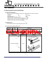
EASTRISING TECHNOLOGY CO., LTD.
m
o
c
.
y
a
l
p
s
i
d
y
u
b
EastRising 旭 日 东 方 科 技 有 限 公 司
ER-OLED0 15-2W
OLED Module User Manual
EastRising Technology Co., Limited
EASTRISING TECHNOLOGY CO., LTD.
m
o
c
.
y
a
l
p
s
i
d
y
u
b
EastRising 旭 日 东 方 科 技 有 限 公 司
Contents
Revision History ................................................................................................................................i
Conttents...........................................................................................................................................ii
1. Basic Specifications................................................................................................................ 1~5
1.1
1.2
1.3
1.4
1.5
1.6
Display Specifications ................................................................................................................. 1
Mechanical Specifications............................................................................................................ 1
Active Area / Memory Mapping & Pixel Construction ...................................................................... 1
Mechanical Drawing.................................................................................................................... 2
Pin Definition ............................................................................................................................. 3
Block Diagram............................................................................................................................ 5
gs ........................................................................................................6
2. Abs
solutte Maximum Rating
3. Optics & Electriical Ch
haractteristics
s ....................................................................................... 7~11
3.1 Optics Characteristics.................................................................................................................. 7
3.2 DC Characteristics ...................................................................................................................... 7
3.3 AC Characteristics....................................................................................................................... 8
3.3.1 68XX-Series MPU Parallel Interface Timing Characteristics.................................................... 8
3.3.2 80XX-Series MPU Parallel Interface Timing Characteristics.................................................... 9
3.3.3 Serial Interface Timing Characteristics .............................................................................. 10
3.3.4 I2C Interface Timing Chara teristics ... ...... .................. ......... ...... ....... ......... .............. 11
pecifiicati n.... ...... ..... ... .... ................... ... ........... .................... ...... ... ......12~14
4. Fun
nctiional Sp
4.1 Commands ................. ...... ....... ........ ..... ....... .... ............ ...... ................ ........... ..... ...... 12
4.2 Power down and Power up Sequence......................................................................................... 12
4.2.1 Power up Sequence ........................................................................................................ 12
4.2.2 Power down Sequence .................................................................................................... 12
4.3 Reset Circuit ............................................................................................................................ 12
4.4 Actual Application Example........................................................................................................ 13
5. Reliability ..................................................................................................................................15
5.1 Contents of Reliability Tests ...................................................................................................... 15
5.2 Failure Check Standard ............................................................................................................. 15
g Qu
uality Co
ontro
ol Speciifications ............................................................................16~19
6. Outtgoing
6.1 Environment Required .............................................................................................................. 16
6.2 Sampling Plan .......................................................................................................................... 16
6.3 Criteria & Acceptable Quality Level............................................................................................. 16
6.3.1 Cosmetic Check (Display Off) in Non-Active Area............................................................... 16
6.3.2 Cosmetic Check (Display Off) in Active Area...................................................................... 18
6.3.3 Pattern Check (Display On) in Active Area......................................................................... 19
e Specifica
ations..............................................................................................................20
7. Package
8. Precautions When Using These OEL Display Modules .......................................................21~23
8.1
8.2
8.3
8.4
8.5
Handling Precautions ................................................................................................................ 21
Storage Precautions.................................................................................................................. 21
Designing Precautions............................................................................................................... 22
Precautions when disposing of the OEL display modules .............................................................. 22
Other Precautions..................................................................................................................... 22
Warranty ........................................................................................................................................23
Notiice .............................................................................................................................................23
ii
EASTRISING TECHNOLOGY CO., LTD.
m
o
c
.
y
a
l
p
s
i
d
y
u
b
EastRising 旭 日 东 方 科 技 有 限 公 司
c Spe
ecifficattion
ns
1. Basic
1.1 Display Specifications
1)
2)
3)
Display Mode:
Display Color:
Drive Duty:
Passive Matrix
Monochrome (White )
1/64 Duty
1.2 Mechanical Specifications
1)
2)
3)
4)
5)
6)
7)
Outline Drawing:
Number of Pixels:
Panel Size:
Active Area:
Pixel Pitch:
Pixel Size:
Weight:
According to the annexed outline drawing
128 × 64
42.04 × 27.22 × 1.45 (mm)
35.052 × 17.516 (mm)
0.274 × 0.274 (mm)
0.254 × 0.254 (mm)
3.28 (g)
1.3 Active Area / Memory Mapping & Pixel Construction
P0.274x128-0.02=35.052 (A/A)
Driver IC M mory Mapping
( ull 128 x 64)
"A"
P0.274x64-0.02=17.516 (A/A)
(0, 0)
Segment 127
( Column 1 )
Common 32
( Row 63 )
Common 63
( Row 1 )
Segment 0
(127, 63)
( Column 128 )
Common 0
( Row 64 )
Common 31
( Row 2 )
0.274
0.254
0.274
0.254
Detail "A"
Scale (10:1)
1
(3)
(2)
0.5±0.5
P0.274x64-0.02 17.516 (A/A)
19.516 (V/A)
21.8 (Polarizer)
23.03±0.2 (Cap Size)
27.22±0.2 (Panel Size)
±0.1
0.3±0.03
4.5±0.5 (Stiffener)
12.5±0.2
1.0
Protective Tape
15x8x0.05mm
W 0.35±0.03
2- φ
Glue
P0.50x(2 -1)=11.5±0.05
24
1.45±0.1
0.274
0.254
( Column 1 )
Segment 127
Segment 0
Detail "A"
Scale (10:1)
25±0.3
3±0.3
6±0.3
(63.22)
36±0.5
ER-OLED015-2 Folding Type OEL Display Module
Pixel Number: 128 x 64, Monochrome, COG Package
( Row 2 )
( Row 64 )
Common 31
( Row 1 )
Common 63
Common 0
( Column 128 )
( Row 63 )
Common 32
Date
20110601
EastRising Technology Co.,Ltd
(2.2)
0.254
0.274
1. Color Light White
2. Driver IC SSD1309
3. FPC Number ER-0205-P05
4. Interface
8-bit 68XX/80XX Parallel, 4-wire SPI, I2C
5. General Tolerance ±0.30
6. The total thickness (1.55 Max) is without polarizer protective film & remove tape.
The actual assembled total thickness with above materials should be 1.80 Max.
0.5±0.1
10.4±0.1
±0.1
Polarizer
t 0.2mm
1
0.8
Remove Tape
t 0.15mm Max
2-φ
5
(1.45)
8.5±0.1
Active Area 1.54"
128 x 64 Pixels
10
(33.85)
(14.77)
"A"
42.04±0.2 (Panel Size)
42.04±0.2 (Cap Size)
41.04 (Polarizer)
37.052 (V/A)
P0.274x128-0.02 35.052 (A/A)
(5.18)
Notes
0.5±0.5
(2.49)
(3.49)
Item
A
5
6
7
8
9
10
11
12
13
1
15
16
17
18
19
20
21
22
23
2
Pn
1
2
3
Symbol
N.C. (GND)
VLSS
VSS
NC
VDD
BS1
BS2
CS#
RES#
D/C#
R/W#
E/RD#
D0
D1
D2
D3
D
D5
D6
D7
IREF
VCOMH
VCC
N.C. (GND)
Remark
Original Drawing
m
o
c
.
y
a
l
p
s
i
d
y
u
b
EastRising 旭 日 东 方 科 技 有 限 公 司
EASTRISING TECHNOLOGY CO., LTD.
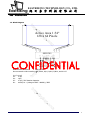
1.4 Mechanical Drawing
Contact Side
8
2
EASTRISING TECHNOLOGY CO., LTD.
m
o
c
.
y
a
l
p
s
i
d
y
u
b
EastRising 旭 日 东 方 科 技 有 限 公 司
1.5 Pin Definition
Symbol
I/O
Function
5
VDD
P
3
VSS
P
23
VCC
P
2
VLSS
P
Power Supply
y for Logic Cirrcuit
This is a voltage supply pin. It must be connected to external source.
Gro
oun
nd of Logic Cirrcuiit
This is a ground pin. It also acts as a reference for the logic pins. It must be
connected to external ground.
Power Supply for OEL Panel
This is the most positive voltage supply pin of the chip. It must be supplied
externally.
Gro
oun
nd of Anallog Circ
cuitt
This is an analog ground pin. It should be connected to VSS externally.
21
IREF
I
22
VCOMH
O
Pin Number
Power Supply
Drriver
Current Reference for Brightness Adjustment
This pin is segment current reference pin. A resistor should be connected
between this pin and VSS. Set the current at 10μA maximum.
put High Leve
el for COM Signa
al
Vo
oltage Outp
This pin is the input pin for the voltage output high level for COM signals. A
capacitor should be connected between this pin and VSS.
ace
Intterfa
6
7
BS1
BS2
I
9
RES#
I
8
CS#
I
10
D/C#
I
12
E/RD#
I
11
R/W#
I
unica
atiing Proto
ocol Sele
ectt
Commu
These pins are MCU interface selection input. See the following table:
BS1
BS2
I2C
0
0
0
4-wi e SPI
8-bit 68XX Parallel
0
1
1
1
8-bit 80XX Para lel
eset for Contrrolle
er and Driv
ver
Power Re
This pin is reset signal input. When the pin is low, initialization of the chip is
executed. Keep this pin pull high during normal operation.
Chip Select
This pin is the chip select input. The chip is enabled for MCU communication only
when CS# is pulled low.
Data/C
Comm
mand Con
ntro
ol
This pin is Data/Command control pin. When the pin is pulled high, the input at
D7~D0 will be interpreted as display data. When the pin is pulled low, the input
at D7~D0 will be transferred to the command register.
When the pin is pulled high and serial interface mode is selected, the data at SDIN
will be interpreted as data. When it is pulled low, the data at SDIN will be
transferred to the command register. In I2C mode, this pin acts as SA0 for slave
address selection.
For detail relationship to MCU interface signals, please refer to the Timing
Characteristics Diagrams.
e Enable or Read
Rea
ad/Write
This pin is MCU interface input.
When interfacing to a 68XX-series
microprocessor, this pin will be used as the Enable (E) signal. Read/write operation
is initiated when this pin is pulled high and the CS# is pulled low.
When connecting to an 80XX-microprocessor, this pin receives the Read (RD#)
signal. Data read operation is initiated when this pin is pulled low and CS# is
pulled low.
When serial or I2C mode is selected, this pin must be connected to VSS.
Rea
ad/Write
e Selec
ct or Write
e
This pin is MCU interface input.
When interfacing to a 68XX-series
microprocessor, this pin will be used as Read/Write (R/W#) selection input. Pull
this pin to “High” for read mode and pull it to “Low” for write mode.
When 80XX interface mode is selected, this pin will be the Write (WR#) input.
Data write operation is initiated when this pin is pulled low and the CS# is pulled
low.
When serial or I2C mode is selected, this pin must be connected to VSS.
3
EASTRISING TECHNOLOGY CO., LTD.
m
o
c
.
y
a
l
p
s
i
d
y
u
b
EastRising 旭 日 东 方 科 技 有 限 公 司
1.5 Pin Definition (Continued)
I/O
Function
D0~D7
I/O
/Outtput Bus
Host Datta Input/
These pins are 8-bit bi-directional data bus to be connected to the
microprocessor’s data bus. When serial mode is selected, D1 will be the serial
data input SDIN and D0 will be the serial clock input SCLK. When I2C mode is
selected, D2, D1 should be tired together and serve as SDAOUT, SDAIN in application
and D0 is the serial clock input, SCL.
Unused pins must be connected to VSS except for D2 in serial mode.
4
N.C.
-
1, 24
N.C. (GND)
-
Pin Number
Symbol
Interface (Continued)
13~20
Re
eserve
e
ed Pin
Res
serve
The N.C. pin between function pins are reserved for compatible and flexible
design.
Reserved Pin (Supporting Pin)
The supporting pins can reduce the influences from stresses on the function pins.
These pins must be connected to external ground as the ESD protection circuit.
4
EASTRISING TECHNOLOGY CO., LTD.
m
o
c
.
y
a
l
p
s
i
d
y
u
b
EastRising 旭 日 东 方 科 技 有 限 公 司
1.6 Block Diagram
~
Common 31
~ ~ ~
Common 0
Segment 0
Segment 127
~
Common 32
Common 63
Active Area 1.54"
128 x 64 Pixels
D7
~
IREF
VCOMH
VCC
D0
VLSS
VSS
VDD
BS1
BS2
CS#
RES#
D/C#
R/W#
E/RD#
SSD1309
C1
C2
R
C5
C3
C4
MCU Interface Selection:
BS1 and BS2
Pins connected to MCU interface: CS#, RES#, D/C#, R/W#, E/RD#, and D0~D7
C1, C3: 0.1μF
C2:
4.7μF
C4:
10μF
C5:
4.7μF / 25V Tantalum Capacitor
R1:
910kΩ, R1 = (Voltage at IREF - BGGND) / IREF
5
EASTRISING TECHNOLOGY CO., LTD.
m
o
c
.
y
a
l
p
s
i
d
y
u
b
EastRising 旭 日 东 方 科 技 有 限 公 司
2. Abso
olute Maxim
mum
m Ratting
gs
Parameter
Symbol
Min
Max
Unit
Notes
Supply Voltage for Logic
VDD
-0.3
4
V
1, 2
Supply Voltage for Display
VCC
0
15
V
1, 2
Operating Temperature
TOP
-40
70
°C
3
Storage Temperature
TSTG
-40
85
°C
3
8,000
-
hour
4
Life Time (80 cd/m )
15,000
-
hour
4
Life Time (60 cd/m2)
25,000
-
hour
4
Life Time (120 cd/m2)
2
Note 1: All the above voltages are on the basis of “VSS = 0V”.
Note 2: When this module is used beyond the above absolute maximum ratings, permanent breakage of the
module may occur. Also, for normal operations, it is desirable to use this module under the
conditions according to Section 3. “Optics & Electrical Characteristics”. If this module is used
beyond these conditions, malfunctioning of the module can occur and the reliability of the module
may deteriorate.
Note 3: The defined temperature ranges do not include the polarizer.
The maximum withstood
temperature of the polarizer should be 80°C.
Note 4: VCC = 12 5V, Ta = 25°C, 50% Checkerboa d.
Software configuration follows Section 4.4 Initialization.
End of lifetime is spe ifi d as 50% of initi l brightness reached. The average operating lifetime at
room temperature is stim ted by the accelerated operation at high temperature conditions.
6
EASTRISING TECHNOLOGY CO., LTD.
m
o
c
.
y
a
l
p
s
i
d
y
u
b
EastRising 旭 日 东 方 科 技 有 限 公 司
3. Optic
cs & Ele
ectriicall Charracterristtics
3.1 Optics Characteristics
Characteristics
Symbol
Conditions
Min
Typ
Max
Unit
Brightness
Lbr
Note 5
100
120
-
cd/m2
(x)
(y)
C.I.E. 1931
0.12
0.22
0.16
0.26
0.20
0.30
-
>10,000:1
-
-
Free
-
degree
Min
Typ
Max
Unit
1.65
2.8
3.3
V
12.0
12.5
13.0
V
C.I.E. (White)
Dark Room Contrast
CR
Viewing Angle
* Optical measurement taken at VDD = 2.8V, VCC = 12.5V.
Software configuration follows Section 4.4 Initialization.
3.2 DC Characteristics
Characteristics
Symbol
Supply Voltage for Logic
VDD
Supply Voltage for Display
VCC
High Level Input
VIH
IOUT = 100μA, 3.3MHz 0.8×VDD
-
VDD
V
Low Level Input
VIL
IOUT = 100μA, 3.3MHz
-
0.2×VDD
V
High Level Output
VOH
IOUT = 100μA, 3.3MHz 0.9×VDD
-
VDD
V
Low Level Output
VOL
IOUT = 100μA, 3.3MHz
0
-
0.1×VDD
V
Operating Current for VDD
IDD
-
180
300
μA
Note 6
-
11.8
14.8
mA
Note 7
-
19.1
23.9
mA
Note 8
-
35.6
44.5
mA
Operating Current for VCC
ICC
Conditions
Note 5
0
Sleep Mode Current for VDD
IDD, SLEEP
-
1
5
μA
Sleep Mode Current for VCC
ICC, SLEEP
-
2
10
μA
Note 5: Brightness (Lbr) and Supply Voltage for Display (VCC) are subject to the change of the panel
characteristics and the customer’s request.
Note 6: VDD = 2.8V, VCC = 12.5V, 30% Display Area Turn on.
Note 7: VDD = 2.8V, VCC = 12.5V, 50% Display Area Turn on.
Note 8: VDD = 2.8V, VCC = 12.5V, 100% Display Area Turn on.
* Software configuration follows Section 4.4 Initialization.
7
EASTRISING TECHNOLOGY CO., LTD.
m
o
c
.
y
a
l
p
s
i
d
y
u
b
EastRising 旭 日 东 方 科 技 有 限 公 司
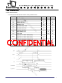
3.3 AC Characteristics
3.3.1 68XX-Series MPU Parallel Interface Timing Characteristics:
Symbol
Description
Min
Max
Unit
Clock Cycle Time
300
-
ns
tAS
Address Setup Time
20
-
ns
tAH
Address Hold Time
0
-
ns
tDW
Data Write Time
80
-
ns
tDSW
Write Data Setup Time
40
-
ns
tDHW
Write Data Hold Time
20
-
ns
tDHR
Read Data Hold Time
20
-
ns
tOH
Output Disable Time
-
70
ns
tACC
Access Time
-
140
ns
-
ns
-
ns
tcycle
PWCSL
PWCSH
Chip Select Low Pulse Width (Read)
120
Chip Select Low Pulse width (Write)
60
Chip Select High Pulse Width (Read)
60
Chip Select High Pulse Width (Write)
60
tR
Rise Time
-
40
ns
tF
Fall Time
-
40
ns
* (VDD - VSS = 1.65V to 3.3V, Ta = 25°C)
8
EASTRISING TECHNOLOGY CO., LTD.
m
o
c
.
y
a
l
p
s
i
d
y
u
b
EastRising 旭 日 东 方 科 技 有 限 公 司
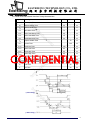
3.3.2 80XX-Series MPU Parallel Interface Timing Characteristics:
Symbol
Description
Min
Max
Unit
Clock Cycle Time
300
-
ns
tAS
Address Setup Time
20
-
ns
tAH
Address Hold Time
0
-
ns
tDW
Data Write Time
70
-
ns
tDSW
Write Data Setup Time
40
-
ns
tDHW
Write Data Hold Time
15
-
ns
tDHR
Read Data Hold Time
20
-
ns
tOH
Output Disable Time
-
70
ns
tACC
Access Time
-
140
ns
tPWLR
Read Low Time
120
-
ns
tPWLW
Write Low Time
60
-
ns
tPWHR
Read High Time
60
-
ns
tPWHW
Write High Time
60
-
ns
tCS
Chip Select Setup Time
0
-
ns
tCSH
Chip Select Hold Time to Read Signal
0
-
ns
tCSF
Chip Select Hold Time
20
-
ns
tcycle
tR
Rise Time
-
40
ns
tF
Fall Time
-
40
ns
* (VDD - VSS = 1.65V to 3.5V, Ta = 25°C)
( Read Timing )
( Write Timing )
9
EASTRISING TECHNOLOGY CO., LTD.
m
o
c
.
y
a
l
p
s
i
d
y
u
b
EastRising 旭 日 东 方 科 技 有 限 公 司
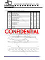
3.3.3 Serial Interface Timing Characteristics: (4-wire SPI)
Symbol
Description
Min
Max
Unit
Clock Cycle Time
100
-
ns
tAS
Address Setup Time
15
-
ns
tAH
Address Hold Time
15
-
ns
tCSS
Chip Select Setup Time
20
-
ns
tCSH
Chip Select Hold Time
50
-
ns
tDW
Data Write Time
55
-
ns
tDSW
Write Data Setup Time
15
-
ns
tDHW
Write Data Hold Time
15
-
ns
tCLKL
Clock Low Time
50
-
ns
tCLKH
Clock High Time
50
-
ns
tcycle
tR
Rise Time
-
40
ns
tF
Fall Time
-
40
ns
* (VDD - VSS = 1.65V to 3.5V, Ta = 25°C)
10
EASTRISING TECHNOLOGY CO., LTD.
m
o
c
.
y
a
l
p
s
i
d
y
u
b
EastRising 旭 日 东 方 科 技 有 限 公 司
3.3.4 Serial Interface Timing Characteristics: (3-wire SPI)
Symbol
Description
Min
Max
Unit
Clock Cycle Time
100
-
ns
tAS
Address Setup Time
15
-
ns
tAH
Address Hold Time
15
-
ns
tCSS
Chip Select Setup Time
20
-
ns
tCSH
Chip Select Hold Time
50
-
ns
tDW
Data Write Time
55
-
ns
tDSW
Write Data Setup Time
15
-
ns
tDHW
Write Data Hold Time
15
-
ns
tCLKL
Clock Low Time
50
-
ns
tCLKH
Clock High Time
50
-
ns
tcycle
tR
Rise Time
-
40
ns
tF
Fall Time
-
40
ns
* (VDD - VSS = 1.65V to 3.5V, Ta = 25°C)
11
EASTRISING TECHNOLOGY CO., LTD.
m
o
c
.
y
a
l
p
s
i
d
y
u
b
EastRising 旭 日 东 方 科 技 有 限 公 司
3.3.5 I2C Interface Timing Characteristics:
Symbol
tcycle
tHSTART
Description
Min
Max
Unit
Clock Cycle Time
2.5
-
μs
Start Condition Hold Time
0.6
-
μs
-
ns
Data Hold Time (for “SDAOUT” Pin)
0
Data Hold Time (for “SDAIN” Pin)
300
Data Setup Time
100
-
ns
tSSTART
Start Condition Setup Time
(Only relevant for a repeated Start condition)
0.6
-
μs
tSSTOP
Stop Condition Setup Time
0.6
-
μs
tHD
tSD
tR
Rise Time for Data and Clock Pin
300
ns
tF
Fall Time for Data and Clock Pin
300
ns
-
μs
tIDLE
Idle Time before a New Transmission can Start
1.3
* (VDD - VSS = 1.65V to 3.5V, Ta = 25°C)
12
EASTRISING TECHNOLOGY CO., LTD.
m
o
c
.
y
a
l
p
s
i
d
y
u
b
EastRising 旭 日 东 方 科 技 有 限 公 司
4. Func
ctio
ona
al Sp
pec
cific
catio
on
4.1 Commands
Refer to the Technical Manual for the SSD1309
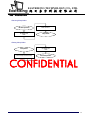
4.2 Power down and Power up Sequence
To protect OEL panel and extend the panel life time, the driver IC power up/down routine should include
a delay period between high voltage and low voltage power sources during turn on/off. It gives the
OEL panel enough time to complete the action of charge and discharge before/after the operation.
4.2.1 Power up Sequence:
1.
2.
3.
4.
5.
6.
Power up VDD
Send Display off command
Initialization
Clear Screen
Power up VCC
Delay 100ms
(When VCC is stable)
7. Send Display on command
VDDD on
VCC on
Display
y on
VCC
VDD
VSS/Ground
Dis
spla
ay off
4.2.2 Power down Sequence:
1. Send Display off command
2. Power down VCC
3. Delay 100ms
(When VCC is reach 0 and panel is completely
discharges)
4. Power down VDD
VCC off
VDD offf
VCC
VDD
VSS/Ground
Note 9:
1) Since an ESD protection circuit is connected between VDD and VCC inside the driver IC, VCC
becomes lower than VDD whenever VDD is ON and VCC is OFF.
2) VCC should be kept float (disable) when it is OFF.
3) Power Pins (VDD, VCC) can never be pulled to ground under any circumstance.
4) VDD should not be power down before VCC power down.
4.3 Reset Circuit
When RES# input is low, the chip is initialized with the following status:
1. Display is OFF
2. 128×64 Display Mode
3. Normal segment and display data column and row address mapping (SEG0 mapped to column
address 00h and COM0 mapped to row address 00h)
4. Shift register data clear in serial interface
5. Display start line is set at display RAM address 0
6. Column address counter is set at 0
7. Normal scan direction of the COM outputs
8. Contrast control register is set at 7Fh
9. Normal display mode (Equivalent to A4h command)
13
EASTRISING TECHNOLOGY CO., LTD.
m
o
c
.
y
a
l
p
s
i
d
y
u
b
EastRising 旭 日 东 方 科 技 有 限 公 司
4.4 Actual Application Example
Command usage and explanation of an actual example
<Power up Sequence>
VDD/VCC off State
Set Display Clock Divide Ratio/Oscillator Frequency
0xD5, 0xA0
Set Pre-Charge Period
0xD9, 0x25
Power up VDD
(RES# as Low State)
Set Multiplex Ratio
0xA8, 0x3F
Set VCOMH Deselect Level
0xDB, 0x34
Power Stabilized
(Delay Recommended)
Set Display Offset
0xD3, 0x00
Set Entire Display On/Off
0xA4
Set RES# as High
(3μs Delay Minimum)
Set Display Start Line
0x40
Set Normal/Inverse Display
0xA6
Initialized State
(Parameters as Default)
Set Segment Re-Map
0xA1
Clear Screen
Comma d Lock
0xFD, 0x12
Set COM Output Scan Direction
0xC8
Power up VCC
(100ms Delay ecommended)
Set Display Off
0xAE
Set COM Pins Hardware Configuration
0xDA, 0x12
Set Display On
0xAF
Initial Settings
Configuration
Set Current Control
0x81, 0xBF
Display Data Sent
If the noise is accidentally occurred at the displaying window during the operation, please reset the
display in order to recover the display function.
<Power down Sequence>
Normal Operation
Power down VCC
(100ms Delay Recommended)
Set Display Off
0xAE
Power down VDD
VDD/VCC off State
13
EASTRISING TECHNOLOGY CO., LTD.
m
o
c
.
y
a
l
p
s
i
d
y
u
b
EastRising 旭 日 东 方 科 技 有 限 公 司
<Entering Sleep Mode>
Normal Operation
Power down VCC
Set Display Off
0xAE
Sleep Mode
<Exiting Sleep Mode>
Sleep Mode
Set Display On
0xAF
Power up VCC
(100ms Delay Recommended)
Normal Operation
14
EASTRISING TECHNOLOGY CO., LTD.
m
o
c
.
y
a
l
p
s
i
d
y
u
b
EastRising 旭 日 东 方 科 技 有 限 公 司
5. Relia
abiliity
5.1 Contents of Reliability Tests
Item
Conditions
High Temperature Operation
70°C, 240 hrs
Low Temperature Operation
-40°C, 240 hrs
High Temperature Storage
85°C, 240 hrs
Low Temperature Storage
-40°C, 240 hrs
High Temperature/Humidity Operation
60°C, 90% RH, 120 hrs
Thermal Shock
-40°C ⇔ 85°C, 24 cycles
60 mins dwell
Criteria
The operational
functions work.
* The samples used for the above tests do not include polarizer.
* No moisture condensation is observed during tests.
5.2 Failure Check Standard
After the completion of the described reliability test, the samples were left at room temperature for 2
hrs prior to conducting the failure test at 23±5°C; 55±15% RH.
15
EASTRISING TECHNOLOGY CO., LTD.
m
o
c
.
y
a
l
p
s
i
d
y
u
b
EastRising 旭 日 东 方 科 技 有 限 公 司
g Qua
ality Control Spe
eciffic
catio
ons
6. Outgoing
6.1 Environment Required
Customer’s test & measurement are required to be conducted under the following conditions:
Temperature:
23 ± 5°C
Humidity:
55 ± 15% RH
Fluorescent Lamp:
30W
≥ 50cm
Distance between the Panel & Lamp:
Distance between the Panel & Eyes of the Inspector: ≥ 30cm
Finger glove (or finger cover) must be worn by the inspector.
Inspection table or jig must be anti-electrostatic.
6.2 Sampling Plan
Level II, Normal Inspection, Single Sampling, MIL-STD-105E
6.3 Criteria & Acceptable Quality Level
Partition
AQL
Definition
Major
0.65
Defects in Pattern Check (Display On)
Minor
1.0
Defects in Cosmetic Check (Display Off)
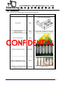
6 3.1 Cosmetic Check (Display Off) in Non-Active Area
Check Item
Classification
Criteria
X > 6 mm (Along with Edge)
Y > 1 mm (Perpendicular to edge)
X
Panel General Chipping
Y
Minor
X
Y
16
EASTRISING TECHNOLOGY CO., LTD.
m
o
c
.
y
a
l
p
s
i
d
y
u
b
EastRising 旭 日 东 方 科 技 有 限 公 司
6.3.1 Cosmetic Check (Display Off) in Non-Active Area (Continued)
Check Item
Classification
Criteria
Any crack is not allowable.
Panel Crack
Minor
Copper Exposed
(Even Pin or Film)
Minor
Film or Trace Damage
Minor
Terminal Lead Prober Mark
Acceptable
Glue or Contamination on Pin
(Couldn’t Be Removed by Alcohol)
Minor
Ink Marking on Back Side of panel
(Exclude on Film)
Acceptable
Not Allowable by Naked Eye Inspection
Ignore for Any
17
EASTRISING TECHNOLOGY CO., LTD.
m
o
c
.
y
a
l
p
s
i
d
y
u
b
EastRising 旭 日 东 方 科 技 有 限 公 司
6.3.2 Cosmetic Check (Display Off) in Active Area
It is recommended to execute in clear room environment (class 10k) if actual in necessary.
Check Item
Classification
Criteria
Any Dirt & Scratch on Polarizer’s
Protective Film
Acceptable
Ignore for not Affect the Polarizer
Scratches, Fiber, Line-Shape Defect
(On Polarizer)
Minor
Dirt, Black Spot, Foreign Material,
(On Polarizer)
Minor
Dent, Bubbles, White spot
(Any Transparent Spot on Polarizer)
Minor
Fingerprint, Flow Mark
(On Polarizer)
Minor
Ignore
W ≤ 0.1
W > 0.1, L ≤ 2
n≤1
L>2
n=0
Φ ≤ 0.1
Ignore
0.1 < Φ ≤ 0.25
n≤1
0.25 < Φ
n=0
Φ ≤ 0.5
Î Ignore if no Influence on Display
0.5 < Φ
n=0
Not Allowable
* P otective film should not be tear off when cosmetic check.
** Definition of W & L & Φ (Unit: mm): Φ = (a + b) / 2
L
W
b: Minor Axis
a: Major Axis
18
EASTRISING TECHNOLOGY CO., LTD.
m
o
c
.
y
a
l
p
s
i
d
y
u
b
EastRising 旭 日 东 方 科 技 有 限 公 司
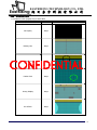
6.3.3 Pattern Check (Display On) in Active Area
Check Item
Classification
No Display
Major
Missing Line
Major
Pixel Short
Major
Darker Pixel
Major
Wrong Display
Major
Un-uniform
Major
Criteria
19
EASTRISING TECHNOLOGY CO., LTD.
m
o
c
.
y
a
l
p
s
i
d
y
u
b
EastRising 旭 日 东 方 科 技 有 限 公 司
7. Pac
ckage
e Spe
eciffic
catiions
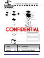
EPE COVER FOAM 351x212x1,
ANTISTATIC x 1 Pcs
x 1 pcs (Empty)
B Pcs Tray Vacuum packing
Module
EPE PROTECTTIVE
x A pcs
Staggered Stacking
Tray 420x285 T=0.8mm
Primary Box C SET
Wrapped with adhesive tape
x B pcs
Vacuum packing bag
EPE PROTECTTIVE
370mm x 280mm x 20mm
CARTON BOX
Label
Primary L450mm x W296 x H110, B wave
x C Pcs
Part ID
Label
Lot ID
Q'ty
QC
Carton Box L464mm x W313mm x H472mm, AB wave
(Major / Maximum)
Item
Quantity
Module
270
per Primary Box
Holding Trays
(A)
15
per Primary Box
Total Trays
(B)
16
per Primary Box (Including 1 Empty Tray)
Primary Box
(C)
1~4
per Carton (4 as Major / Maximum)
20
EASTRISING TECHNOLOGY CO., LTD.
m
o
c
.
y
a
l
p
s
i
d
y
u
b
EastRising 旭 日 东 方 科 技 有 限 公 司
ecautiions
s Wh
hen
n Using These OEL
L Dis
splay Module
es
8. Pre
8.1 Handling Precautions
1)
2)
3)
4)
5)
6)
Since the display panel is being made of glass, do not apply mechanical impacts such us dropping
from a high position.
If the display panel is broken by some accident and the internal organic substance leaks out, be
careful not to inhale nor lick the organic substance.
If pressure is applied to the display surface or its neighborhood of the OEL display module, the cell
structure may be damaged and be careful not to apply pressure to these sections.
The polarizer covering the surface of the OEL display module is soft and easily scratched. Please
be careful when handling the OEL display module.
When the surface of the polarizer of the OEL display module has soil, clean the surface. It takes
advantage of by using following adhesion tape.
* Scotch Mending Tape No. 810 or an equivalent
Never try to breathe upon the soiled surface nor wipe the surface using cloth containing solvent
such as ethyl alcohol, since the surface of the polarizer will become cloudy.
Also, pay attention that the following liquid and solvent may spoil the polarizer:
* Water
* Ketone
* Aromatic Solvents
Hold OEL display module very carefully when placing OEL display module into the system housing.
Do not apply excessive stress or pressure to OEL display module. And, do not over bend the film
with electrode patt rn layouts. These stresses will influence the display performance Also,
secure sufficient rigidity for the outer cases.
7)
8)
9)
10)
Do not apply stress to the driver IC and the surrounding molded sections.
Do not disassemble nor modify the OEL display module.
Do not apply input signals while the logic power is off.
Pay sufficient attention to the working environments when handing OEL display modules to prevent
occurrence of element breakage accidents by static electricity.
* Be sure to make human body grounding when handling OEL display modules.
* Be sure to ground tools to use or assembly such as soldering irons.
* To suppress generation of static electricity, avoid carrying out assembly work under dry
environments.
* Protective film is being applied to the surface of the display panel of the OEL display module.
Be careful since static electricity may be generated when exfoliating the protective film.
11) Protection film is being applied to the surface of the display panel and removes the protection film
before assembling it. At this time, if the OEL display module has been stored for a long period of
time, residue adhesive material of the protection film may remain on the surface of the display
panel after removed of the film. In such case, remove the residue material by the method
introduced in the above Section 5).
12) If electric current is applied when the OEL display module is being dewed or when it is placed under
high humidity environments, the electrodes may be corroded and be careful to avoid the above.
8.2 Storage Precautions
1)
When storing OEL display modules, put them in static electricity preventive bags avoiding exposure
to direct sun light nor to lights of fluorescent lamps. and, also, avoiding high temperature and high
21
EASTRISING TECHNOLOGY CO., LTD.
m
o
c
.
y
a
l
p
s
i
d
y
u
b
EastRising 旭 日 东 方 科 技 有 限 公 司
2)
humidity environment or low temperature (less than 0°C) environments. (We recommend you to
store these modules in the packaged state when they were shipped from WiseChip Semiconductor
Inc.)
At that time, be careful not to let water drops adhere to the packages or bags nor let dewing occur
with them.
If electric current is applied when water drops are adhering to the surface of the OEL display
module, when the OEL display module is being dewed or when it is placed under high humidity
environments, the electrodes may be corroded and be careful about the above.
8.3 Designing Precautions
1)
2)
3)
4)
5)
6)
7)
8)
The absolute maximum ratings are the ratings which cannot be exceeded for OEL display module,
and if these values are exceeded, panel damage may be happen.
To prevent occurrence of malfunctioning by noise, pay attention to satisfy the VIL and VIH
specifications and, at the same time, to make the signal line cable as short as possible.
We recommend you to install excess current preventive unit (fuses, etc.) to the power circuit (VDD).
(Recommend value: 0.5A)
Pay sufficient attention to avoid occurrence of mutual noise interference with the neighboring
devices.
As for EMI, take necessary measures on the equipment side basically.
When fastening the OEL display module, fasten the external plastic housing section.
If power supply to the OEL display module is forcibly shut down by such errors as taking out the
main battery while the OEL displ y panel is in ope ation, we can ot gua antee the quality of this
OEL display module.
The electric potential to be connected to the rear face of the IC chip should be as follows: SSD1309
* Connection (contact) to any other potential than the above may lead to rupture of the IC.
8.4 Precautions when disposing of the OEL display modules
1)
Request the qualified companies to handle industrial wastes when disposing of the OEL display
modules. Or, when burning them, be sure to observe the environmental and hygienic laws and
regulations.
8.5 Other Precautions
1)
2)
3)
4)
5)
When an OEL display module is operated for a long of time with fixed pattern may remain as an
after image or slight contrast deviation may occur.
Nonetheless, if the operation is interrupted and left unused for a while, normal state can be
restored. Also, there will be no problem in the reliability of the module.
To protect OEL display modules from performance drops by static electricity rapture, etc., do not
touch the following sections whenever possible while handling the OEL display modules.
* Pins and electrodes
* Pattern layouts such as the FPC
With this OEL display module, the OEL driver is being exposed.
Generally speaking,
semiconductor elements change their characteristics when light is radiated according to the
principle of the solar battery. Consequently, if this OEL driver is exposed to light, malfunctioning
may occur.
* Design the product and installation method so that the OEL driver may be shielded from light in
actual usage.
* Design the product and installation method so that the OEL driver may be shielded from light
during the inspection processes.
Although this OEL display module stores the operation state data by the commands and the
indication data, when excessive external noise, etc. enters into the module, the internal status may
be changed. It therefore is necessary to take appropriate measures to suppress noise generation
or to protect from influences of noise on the system design.
We recommend you to construct its software to make periodical refreshment of the operation
22