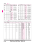
1
CP3210
Single PowerPC 750FX
User’s Guide
CA.DT.A57−1eOctobre 2008
CP3210 User’s Guide
Preface
Revision History
Publication Title: CP3210 User’s Guide
Doc. ID: SD.DT.A57−1e
Rev.
Brief Description of Changes
Date of Issue
0e
Initial Version
September 2008
1e
Chapter 4: User and System Flash EPROM, PLD control register October 2008
Copyright © 2008 Kontron AG. All rights reserved. All data is for information purposes only and not guaranteed
for legal purposes. Information has been carefully checked and is believed to be accurate; however, no
responsibility is assumed for inaccuracies. Kontron and the Kontron logo and all other trademarks or registered
trademarks are the property of their respective owners and are recognized. Specifications are subject to change
without notice.
Page i
SD.DT.A57−1e
Preface
CP3210 User’s Guide
Table Of Contents
Chapter 1 −
Introduction . . . . . . . . . . . . . . . . . . . . . . . . . . . . . . . . . . . . . . . . . . . . . . . . . . . . . . . . .
1
1.1
Objectives . . . . . . . . . . . . . . . . . . . . . . . . . . . . . . . . . . . . . . . . . . . . . . . . . . . . . . . . . . . . . . . . . . . . . . . . .
2
1.2
Audience . . . . . . . . . . . . . . . . . . . . . . . . . . . . . . . . . . . . . . . . . . . . . . . . . . . . . . . . . . . . . . . . . . . . . . . . . .
2
1.3
Scope . . . . . . . . . . . . . . . . . . . . . . . . . . . . . . . . . . . . . . . . . . . . . . . . . . . . . . . . . . . . . . . . . . . . . . . . . . . . .
2
1.4
Structure . . . . . . . . . . . . . . . . . . . . . . . . . . . . . . . . . . . . . . . . . . . . . . . . . . . . . . . . . . . . . . . . . . . . . . . . . .
3
1.5
Conventions . . . . . . . . . . . . . . . . . . . . . . . . . . . . . . . . . . . . . . . . . . . . . . . . . . . . . . . . . . . . . . . . . . . . . . .
4
1.6
Related Documents . . . . . . . . . . . . . . . . . . . . . . . . . . . . . . . . . . . . . . . . . . . . . . . . . . . . . . . . . . . . . . . . .
5
1.7
World Wide Web Sites . . . . . . . . . . . . . . . . . . . . . . . . . . . . . . . . . . . . . . . . . . . . . . . . . . . . . . . . . . . . . .
5
Chapter 2 −
General Information . . . . . . . . . . . . . . . . . . . . . . . . . . . . . . . . . . . . . . . . . . . . . . . . .
6
2.1
Introduction . . . . . . . . . . . . . . . . . . . . . . . . . . . . . . . . . . . . . . . . . . . . . . . . . . . . . . . . . . . . . . . . . . . . . . .
6
2.2
Main Features . . . . . . . . . . . . . . . . . . . . . . . . . . . . . . . . . . . . . . . . . . . . . . . . . . . . . . . . . . . . . . . . . . . . . .
8
2.3
Inputs/Outputs . . . . . . . . . . . . . . . . . . . . . . . . . . . . . . . . . . . . . . . . . . . . . . . . . . . . . . . . . . . . . . . . . . . . .
9
2.4
Operating System Support . . . . . . . . . . . . . . . . . . . . . . . . . . . . . . . . . . . . . . . . . . . . . . . . . . . . . . . . . .
9
Chapter 3 −
Preparing Before Using . . . . . . . . . . . . . . . . . . . . . . . . . . . . . . . . . . . . . . . . . . . . . . 10
3.1
Preventing Static Electricity Discharge . . . . . . . . . . . . . . . . . . . . . . . . . . . . . . . . . . . . . . . . . . . . . . . 10
3.2
Unpacking . . . . . . . . . . . . . . . . . . . . . . . . . . . . . . . . . . . . . . . . . . . . . . . . . . . . . . . . . . . . . . . . . . . . . . . . . 11
3.3
Inspection . . . . . . . . . . . . . . . . . . . . . . . . . . . . . . . . . . . . . . . . . . . . . . . . . . . . . . . . . . . . . . . . . . . . . . . . . 11
3.4
Board Identification . . . . . . . . . . . . . . . . . . . . . . . . . . . . . . . . . . . . . . . . . . . . . . . . . . . . . . . . . . . . . . . . 12
Chapter 4 −
Functional Description . . . . . . . . . . . . . . . . . . . . . . . . . . . . . . . . . . . . . . . . . . . . . . . 15
4.1
CP3210 Block Diagram . . . . . . . . . . . . . . . . . . . . . . . . . . . . . . . . . . . . . . . . . . . . . . . . . . . . . . . . . . . . . 15
4.2
General Description . . . . . . . . . . . . . . . . . . . . . . . . . . . . . . . . . . . . . . . . . . . . . . . . . . . . . . . . . . . . . . . . 16
4.2.1
4.2.2
4.2.3
4.2.4
4.2.5
4.2.6
4.2.7
4.2.8
4.2.9
4.2.10
Host Bridge . . . . . . . . . . . . . . . . . . . . . . . . . . . . . . . . . . . . . . . . . . . . . . . . . . . . . . . . . . . . . . . . . . . . .
Processor . . . . . . . . . . . . . . . . . . . . . . . . . . . . . . . . . . . . . . . . . . . . . . . . . . . . . . . . . . . . . . . . . . . . . . .
Memory . . . . . . . . . . . . . . . . . . . . . . . . . . . . . . . . . . . . . . . . . . . . . . . . . . . . . . . . . . . . . . . . . . . . . . . . .
PLD Control Register . . . . . . . . . . . . . . . . . . . . . . . . . . . . . . . . . . . . . . . . . . . . . . . . . . . . . . . . . . . . .
Ethernet Controllers . . . . . . . . . . . . . . . . . . . . . . . . . . . . . . . . . . . . . . . . . . . . . . . . . . . . . . . . . . . . . .
EIA−232 Serial I/O Controller . . . . . . . . . . . . . . . . . . . . . . . . . . . . . . . . . . . . . . . . . . . . . . . . . . . . . . .
EIA−422/EIA−485 Serial I/O Controller . . . . . . . . . . . . . . . . . . . . . . . . . . . . . . . . . . . . . . . . . . . . . . .
Thermal Sensor . . . . . . . . . . . . . . . . . . . . . . . . . . . . . . . . . . . . . . . . . . . . . . . . . . . . . . . . . . . . . . . . . .
JTAG/Boundary−Scan . . . . . . . . . . . . . . . . . . . . . . . . . . . . . . . . . . . . . . . . . . . . . . . . . . . . . . . . . . . . .
System Frequency Selection . . . . . . . . . . . . . . . . . . . . . . . . . . . . . . . . . . . . . . . . . . . . . . . . . . . . . .
Chapter 5 −
16
18
19
21
22
23
23
23
23
23
Connectors . . . . . . . . . . . . . . . . . . . . . . . . . . . . . . . . . . . . . . . . . . . . . . . . . . . . . . . . . 24
5.1
J1 Connector Pin Assignment . . . . . . . . . . . . . . . . . . . . . . . . . . . . . . . . . . . . . . . . . . . . . . . . . . . . . . . 25
5.2
J2 Connector Pin Assignment . . . . . . . . . . . . . . . . . . . . . . . . . . . . . . . . . . . . . . . . . . . . . . . . . . . . . . . 26
CA.DT.A57−1e
Page ii
Preface
5.3
CP3210 User’s Guide
Geographical Address Pin Assignment . . . . . . . . . . . . . . . . . . . . . . . . . . . . . . . . . . . . . . . . . . . . . . 27
5.4 PMC Connector Pin Assignment . . . . . . . . . . . . . . . . . . . . . . . . . . . . . . . . . . . . . . . . . . . . . . . . . . . .
5.4.1 J11 Connector Pin Assignment . . . . . . . . . . . . . . . . . . . . . . . . . . . . . . . . . . . . . . . . . . . . . . . . . . . . .
5.4.2 J12 Connector Pin Assignment . . . . . . . . . . . . . . . . . . . . . . . . . . . . . . . . . . . . . . . . . . . . . . . . . . . .
5.4.3 J14 Connector Pin Assignment . . . . . . . . . . . . . . . . . . . . . . . . . . . . . . . . . . . . . . . . . . . . . . . . . . . .
28
28
28
29
5.5
PCI and Additional CompactPCI Signal Description . . . . . . . . . . . . . . . . . . . . . . . . . . . . . . . . . . . 30
5.6
Other Signal Description . . . . . . . . . . . . . . . . . . . . . . . . . . . . . . . . . . . . . . . . . . . . . . . . . . . . . . . . . . . . 32
5.7
P3 Connector Pin Assignment . . . . . . . . . . . . . . . . . . . . . . . . . . . . . . . . . . . . . . . . . . . . . . . . . . . . . . 33
5.8
P4 Connector Pin Assignment . . . . . . . . . . . . . . . . . . . . . . . . . . . . . . . . . . . . . . . . . . . . . . . . . . . . . . 34
Chapter 6 −
PMC Site . . . . . . . . . . . . . . . . . . . . . . . . . . . . . . . . . . . . . . . . . . . . . . . . . . . . . . . . . . . . 35
6.1
Description . . . . . . . . . . . . . . . . . . . . . . . . . . . . . . . . . . . . . . . . . . . . . . . . . . . . . . . . . . . . . . . . . . . . . . . . 35
6.2
Signaling Voltage Keying Pin . . . . . . . . . . . . . . . . . . . . . . . . . . . . . . . . . . . . . . . . . . . . . . . . . . . . . . . 36
6.3
PMC Installation . . . . . . . . . . . . . . . . . . . . . . . . . . . . . . . . . . . . . . . . . . . . . . . . . . . . . . . . . . . . . . . . . . . . 37
Chapter 7 −
System Installation . . . . . . . . . . . . . . . . . . . . . . . . . . . . . . . . . . . . . . . . . . . . . . . . . . 38
7.1
Power Supply Units . . . . . . . . . . . . . . . . . . . . . . . . . . . . . . . . . . . . . . . . . . . . . . . . . . . . . . . . . . . . . . . . 38
7.2
Power Up Specifications . . . . . . . . . . . . . . . . . . . . . . . . . . . . . . . . . . . . . . . . . . . . . . . . . . . . . . . . . . . . 38
7.3
+5V Power Specifications . . . . . . . . . . . . . . . . . . . . . . . . . . . . . . . . . . . . . . . . . . . . . . . . . . . . . . . . . . . 39
7.4
+3.3V Power Specifications . . . . . . . . . . . . . . . . . . . . . . . . . . . . . . . . . . . . . . . . . . . . . . . . . . . . . . . . . 39
7.5
V(I/O) Power Recommendations . . . . . . . . . . . . . . . . . . . . . . . . . . . . . . . . . . . . . . . . . . . . . . . . . . . . . 39
7.6
V(I/O) PMC Power Specifications . . . . . . . . . . . . . . . . . . . . . . . . . . . . . . . . . . . . . . . . . . . . . . . . . . . . 39
7.7
12VPower Specifications . . . . . . . . . . . . . . . . . . . . . . . . . . . . . . . . . . . . . . . . . . . . . . . . . . . . . . . . . . . . 39
7.8
Chassis Ground Specifications . . . . . . . . . . . . . . . . . . . . . . . . . . . . . . . . . . . . . . . . . . . . . . . . . . . . . . 39
7.9
System Configuration Suggestions . . . . . . . . . . . . . . . . . . . . . . . . . . . . . . . . . . . . . . . . . . . . . . . . . . 39
Chapter 8 −
Operating Instructions . . . . . . . . . . . . . . . . . . . . . . . . . . . . . . . . . . . . . . . . . . . . . . . 40
8.1
Power−up . . . . . . . . . . . . . . . . . . . . . . . . . . . . . . . . . . . . . . . . . . . . . . . . . . . . . . . . . . . . . . . . . . . . . . . . . . 40
8.2
Reset Switch . . . . . . . . . . . . . . . . . . . . . . . . . . . . . . . . . . . . . . . . . . . . . . . . . . . . . . . . . . . . . . . . . . . . . . . 40
8.3
LEDs . . . . . . . . . . . . . . . . . . . . . . . . . . . . . . . . . . . . . . . . . . . . . . . . . . . . . . . . . . . . . . . . . . . . . . . . . . . . . . 41
8.4
Memory Map by U−Boot Firmware . . . . . . . . . . . . . . . . . . . . . . . . . . . . . . . . . . . . . . . . . . . . . . . . . . . 42
8.5
Hardware Reset . . . . . . . . . . . . . . . . . . . . . . . . . . . . . . . . . . . . . . . . . . . . . . . . . . . . . . . . . . . . . . . . . . . . 44
8.6
Software Reset . . . . . . . . . . . . . . . . . . . . . . . . . . . . . . . . . . . . . . . . . . . . . . . . . . . . . . . . . . . . . . . . . . . . . 45
8.7
PCI Configuration . . . . . . . . . . . . . . . . . . . . . . . . . . . . . . . . . . . . . . . . . . . . . . . . . . . . . . . . . . . . . . . . . . 46
Chapter 9 −
Inserting and Removing the Board . . . . . . . . . . . . . . . . . . . . . . . . . . . . . . . . . . . . 47
9.1
Inserting the Board . . . . . . . . . . . . . . . . . . . . . . . . . . . . . . . . . . . . . . . . . . . . . . . . . . . . . . . . . . . . . . . . . 47
9.2
Removing the Board . . . . . . . . . . . . . . . . . . . . . . . . . . . . . . . . . . . . . . . . . . . . . . . . . . . . . . . . . . . . . . . . 48
Page iii
CA.DT.A57−1e
CP3210 User’s Guide
Chapter 10 −
Preface
I/O Transition Module . . . . . . . . . . . . . . . . . . . . . . . . . . . . . . . . . . . . . . . . . . . . . . . . 49
10.1 Installing the CP3210 I/O Transition Module . . . . . . . . . . . . . . . . . . . . . . . . . . . . . . . . . . . . . . . . . . 50
10.2 Reset Switch . . . . . . . . . . . . . . . . . . . . . . . . . . . . . . . . . . . . . . . . . . . . . . . . . . . . . . . . . . . . . . . . . . . . . . . 50
10.3 Links and GPIOs . . . . . . . . . . . . . . . . . . . . . . . . . . . . . . . . . . . . . . . . . . . . . . . . . . . . . . . . . . . . . . . . . . . 51
10.4 Connectors . . . . . . . . . . . . . . . . . . . . . . . . . . . . . . . . . . . . . . . . . . . . . . . . . . . . . . . . . . . . . . . . . . . . . . . .
10.4.1 RJ1 Connector Pin Assignment . . . . . . . . . . . . . . . . . . . . . . . . . . . . . . . . . . . . . . . . . . . . . . . . . . . .
10.4.2 RJ2 Connector Pin Assignment . . . . . . . . . . . . . . . . . . . . . . . . . . . . . . . . . . . . . . . . . . . . . . . . . . . .
10.4.3 H1 (JTAG_CPCI) Connector Pin Assignment . . . . . . . . . . . . . . . . . . . . . . . . . . . . . . . . . . . . . . . .
10.4.4 H3 (EIA−232) Connector Pin Assignment . . . . . . . . . . . . . . . . . . . . . . . . . . . . . . . . . . . . . . . . . . . .
10.4.5 H4 (EIA−485) Connector Pin Assignment . . . . . . . . . . . . . . . . . . . . . . . . . . . . . . . . . . . . . . . . . . . .
10.4.6 H5 (10/100/1000BASE−T) Connector Pin Assignment (ETH0) . . . . . . . . . . . . . . . . . . . . . . . . . .
10.4.7 H6 (10/100BASE−T) Connector Pin Assignment (ETH1) . . . . . . . . . . . . . . . . . . . . . . . . . . . . . . .
10.4.8 PMC Connectors Pin Assignment . . . . . . . . . . . . . . . . . . . . . . . . . . . . . . . . . . . . . . . . . . . . . . . . . .
52
53
54
55
56
56
57
57
58
Appendix A − Specifications . . . . . . . . . . . . . . . . . . . . . . . . . . . . . . . . . . . . . . . . . . . . . . . . . . . . . . . 59
A.1
Local Resources . . . . . . . . . . . . . . . . . . . . . . . . . . . . . . . . . . . . . . . . . . . . . . . . . . . . . . . . . . . . . . . . . .
59
A.2
Power Requirements . . . . . . . . . . . . . . . . . . . . . . . . . . . . . . . . . . . . . . . . . . . . . . . . . . . . . . . . . . . . . .
60
A.3
EMC Regulatory Compliance and Safety . . . . . . . . . . . . . . . . . . . . . . . . . . . . . . . . . . . . . . . . . . . .
60
A.4
Flammability Rating . . . . . . . . . . . . . . . . . . . . . . . . . . . . . . . . . . . . . . . . . . . . . . . . . . . . . . . . . . . . . . .
60
A.5 Environmental Specifications . . . . . . . . . . . . . . . . . . . . . . . . . . . . . . . . . . . . . . . . . . . . . . . . . . . . . . 61
A.5.1 Operating Environment . . . . . . . . . . . . . . . . . . . . . . . . . . . . . . . . . . . . . . . . . . . . . . . . . . . . . . . . . . . 61
A.5.2 Storage Environment . . . . . . . . . . . . . . . . . . . . . . . . . . . . . . . . . . . . . . . . . . . . . . . . . . . . . . . . . . . . . 61
A.6
MTBF Data . . . . . . . . . . . . . . . . . . . . . . . . . . . . . . . . . . . . . . . . . . . . . . . . . . . . . . . . . . . . . . . . . . . . . . . .
62
A.7
Mechanical Construction . . . . . . . . . . . . . . . . . . . . . . . . . . . . . . . . . . . . . . . . . . . . . . . . . . . . . . . . . .
63
Appendix B − Troubleshooting . . . . . . . . . . . . . . . . . . . . . . . . . . . . . . . . . . . . . . . . . . . . . . . . . . . . . 64
B.1
Step 1 − No Power . . . . . . . . . . . . . . . . . . . . . . . . . . . . . . . . . . . . . . . . . . . . . . . . . . . . . . . . . . . . . . . . .
64
B.2
Step 2 − Power On, Unexpected Behaviour . . . . . . . . . . . . . . . . . . . . . . . . . . . . . . . . . . . . . . . . . .
64
B.3
Step 3 − Power On, No Terminal Display . . . . . . . . . . . . . . . . . . . . . . . . . . . . . . . . . . . . . . . . . . . . .
64
B.4
Step 4 − CP3210 Locks−up . . . . . . . . . . . . . . . . . . . . . . . . . . . . . . . . . . . . . . . . . . . . . . . . . . . . . . . . . .
65
B.5
When Phoning, Faxing or E−Mailing for Technical Support, Be Prepared To Give . . . . . .
65
Glossaire . . . . . . . . . . . . . . . . . . . . . . . . . . . . . . . . . . . . . . . . . . . . . . . . . . . . . . . . . . . . . . . . . . . . . . . . . 66
CA.DT.A57−1e
Page iv
Preface
CP3210 User’s Guide
List Of Figures
Figure 1: View of the CP3210 . . . . . . . . . . . . . . . . . . . . . . . . . . . . . . . . . . . . . . . . . . . . . . . . . . . . . . . . . . . . . . . . .
1
Figure 2: Top view of the CP3210 without the ruggedizer . . . . . . . . . . . . . . . . . . . . . . . . . . . . . . . . . . . . . . . . .
7
Figure 3: Bottom view of the CP3210 without the ruggedizer . . . . . . . . . . . . . . . . . . . . . . . . . . . . . . . . . . . . . .
7
Figure 4: Top Side Identification Labels . . . . . . . . . . . . . . . . . . . . . . . . . . . . . . . . . . . . . . . . . . . . . . . . . . . . . . . . . 12
Figure 5: Bottom Side Identification Labels . . . . . . . . . . . . . . . . . . . . . . . . . . . . . . . . . . . . . . . . . . . . . . . . . . . . . . 13
Figure 6: Ruggedizer Identification Label . . . . . . . . . . . . . . . . . . . . . . . . . . . . . . . . . . . . . . . . . . . . . . . . . . . . . . . 14
Figure 7: CP3210 Block Diagram . . . . . . . . . . . . . . . . . . . . . . . . . . . . . . . . . . . . . . . . . . . . . . . . . . . . . . . . . . . . . . 15
Figure 8: 10/100−Mb/s Ethernet Controller . . . . . . . . . . . . . . . . . . . . . . . . . . . . . . . . . . . . . . . . . . . . . . . . . . . . . . 22
Figure 9: CP3210 Onboard Connector Locations . . . . . . . . . . . . . . . . . . . . . . . . . . . . . . . . . . . . . . . . . . . . . . . . 24
Figure 10: COP JTAG Equipment . . . . . . . . . . . . . . . . . . . . . . . . . . . . . . . . . . . . . . . . . . . . . . . . . . . . . . . . . . . . . . 33
Figure 11: +3.3V PMC . . . . . . . . . . . . . . . . . . . . . . . . . . . . . . . . . . . . . . . . . . . . . . . . . . . . . . . . . . . . . . . . . . . . . . . 36
Figure 12: Universal PMC . . . . . . . . . . . . . . . . . . . . . . . . . . . . . . . . . . . . . . . . . . . . . . . . . . . . . . . . . . . . . . . . . . . . 36
Figure 13: PMC Slot . . . . . . . . . . . . . . . . . . . . . . . . . . . . . . . . . . . . . . . . . . . . . . . . . . . . . . . . . . . . . . . . . . . . . . . . . 37
Figure 14: LEDs Setting . . . . . . . . . . . . . . . . . . . . . . . . . . . . . . . . . . . . . . . . . . . . . . . . . . . . . . . . . . . . . . . . . . . . . . 41
Figure 15: CP3210 Hardware Reset Block Diagram . . . . . . . . . . . . . . . . . . . . . . . . . . . . . . . . . . . . . . . . . . . . . . 44
Figure 16: Inserting the Board . . . . . . . . . . . . . . . . . . . . . . . . . . . . . . . . . . . . . . . . . . . . . . . . . . . . . . . . . . . . . . . . . 47
Figure 17: Removing the Board . . . . . . . . . . . . . . . . . . . . . . . . . . . . . . . . . . . . . . . . . . . . . . . . . . . . . . . . . . . . . . . 48
Figure 18: CP3210 I/O Transition Module . . . . . . . . . . . . . . . . . . . . . . . . . . . . . . . . . . . . . . . . . . . . . . . . . . . . . . . 49
Figure 19: CP3210 I/O Transition Module . . . . . . . . . . . . . . . . . . . . . . . . . . . . . . . . . . . . . . . . . . . . . . . . . . . . . . . 51
Figure 20: CP3210 I/O Transition Module Connectors . . . . . . . . . . . . . . . . . . . . . . . . . . . . . . . . . . . . . . . . . . . . 52
Figure 21: CP3210 I/O Transition Module Front Panel . . . . . . . . . . . . . . . . . . . . . . . . . . . . . . . . . . . . . . . . . . . . 52
Figure 22: CP3210 Dimensions . . . . . . . . . . . . . . . . . . . . . . . . . . . . . . . . . . . . . . . . . . . . . . . . . . . . . . . . . . . . . . . 63
Page v
CA.DT.A57−1e
Preface
CP3210 User’s Guide
List Of Tables
Table 1: Order Code . . . . . . . . . . . . . . . . . . . . . . . . . . . . . . . . . . . . . . . . . . . . . . . . . . . . . . . . . . . . . . . . . . . . . . . . .
6
Table 2: PMC Site Information . . . . . . . . . . . . . . . . . . . . . . . . . . . . . . . . . . . . . . . . . . . . . . . . . . . . . . . . . . . . . . . . . 35
Table 3: LEDs Description . . . . . . . . . . . . . . . . . . . . . . . . . . . . . . . . . . . . . . . . . . . . . . . . . . . . . . . . . . . . . . . . . . . . 41
Table 4: CP3210 Memory Map Setup by U−Boot . . . . . . . . . . . . . . . . . . . . . . . . . . . . . . . . . . . . . . . . . . . . . . . . 43
Table 5: Reset Generated by the Hard Reset Sources . . . . . . . . . . . . . . . . . . . . . . . . . . . . . . . . . . . . . . . . . . . . 45
Table 6: PCI0 Accesses . . . . . . . . . . . . . . . . . . . . . . . . . . . . . . . . . . . . . . . . . . . . . . . . . . . . . . . . . . . . . . . . . . . . . . 46
Table 7: PCI1 Accesses . . . . . . . . . . . . . . . . . . . . . . . . . . . . . . . . . . . . . . . . . . . . . . . . . . . . . . . . . . . . . . . . . . . . . . 46
Table 8: Default Link Settings . . . . . . . . . . . . . . . . . . . . . . . . . . . . . . . . . . . . . . . . . . . . . . . . . . . . . . . . . . . . . . . . . 51
CA.DT.A57−1e
Page vi
Preface
CP3210 User’s Guide
Proprietary Note
This document contains information proprietary to Kontron. It may not be copied or transmitted by any means,
disclosed to others, or stored in any retrieval system or media without the prior written consent of Kontron or one
of its authorized agents.
The information contained in this document is, to the best of our knowledge, entirely correct. However, Kontron
cannot accept liability for any inaccuracies or the consequences thereof, or for any liability arising from the use
or application of any circuit, product, or example shown in this document.
Kontron reserves the right to change, modify, or improve this document or the product described herein, as seen
fit by Kontron without further notice.
Trademarks
This document may include names, company logos and trademarks, which are registered trademarks and,
therefore, proprietary to their respective owners.
Environmental Protection Statement
This product has been manufactured to satisfy environmental protection requirements where possible. Many of
the components used (structural parts, printed circuit boards, connectors, batteries, etc.) are capable of being
recycled.
Final disposition of this product after its service life must be accomplished in accordance with applicable country,
state, or local laws or regulations.
The Waste Electrical and Electronic Equipment (WEEE) Directive aims to:
> reduce waste arising from electrical and electronic equipment (EEE)
> make producers of EEE responsible for the environmental impact of their products, especially when they
become waste
> encourage separate collection and subsequent treatment, reuse, recovery, recycling and sound
environmental disposal of EEE
> improve the environmental performance of all those involved during the lifecycle of EEE
Page vii
CA.DT.A57−1e
CP3210 User’s Guide
Preface
Conventions
This guide uses several types of notice: Note, Caution, ESD.
Note: this notice calls attention to important features or instructions.
Caution: this notice alert you to system damage, loss of data, or risk of personal injury.
ESD: This banner indicates an Electrostatic Sensitive Device.
All numbers are expressed in decimal, except addresses and memory or register data, which are expressed in
hexadecimal. The prefix ‘0x’ shows a hexadecimal number, following the ‘C’ programming language convention.
The multipliers ‘k’, ‘M’ and ‘G’ have their conventional scientific and engineering meanings of *103, *106 and *109
respectively. The only exception to this is in the description of the size of memory areas, when ‘K’, ‘M’ and ‘G’
mean *210, *220 and *230 respectively.
When describing transfer rates, ‘k’ ‘M’ and ‘G’ mean *103, *106 and *109 not *2 10 *2 20 and *2 30.
In PowerPC terminology, multiple bit fields are numbered from 0 to n, where 0 is the MSB and n is the LSB. PCI
and CompactPCI terminology follows the more familiar convention that bit 0 is the LSB and n is the MSB.
Signal names ending with an asterisk (*) or a hash (#) denote active low signals; all other signals are active high.
Signal names follow the PICMG 2.0 R3.0 CompactPCI Specification and the PCI Local Bus 2.3 Specification.
For Your Safety
Your new Kontron product was developed and tested carefully to provide all features necessary to ensure its
compliance with electrical safety requirements. It was also designed for a long fault−free life. However, the life
expectancy of your product can be drastically reduced by improper treatment during unpacking and installation.
Therefore, in the interest of your own safety and of the correct operation of your new Kontron product, you are
requested to conform with the following guidelines.
High Voltage Safety Instructions
Warning!
All operations on this device must be carried out by sufficiently skilled personnel only.
Caution, Electric Shock!
Before installing a not hot−swappable Kontron product into a system always ensure that your mains power
is switched off. This applies also to the installation of piggybacks. Serious electrical shock hazards can
exist during all installation, repair and maintenance operations with this product. Therefore, always unplug
the power cable and any other cables which provide external voltages before performing work.
CA.DT.A57−1e
Page viii
Preface
CP3210 User’s Guide
Special Handling and Unpacking Instructions
ESD Sensitive Device!
Electronic boards and their components are sensitive to static electricity. Therefore, care must be taken
during all handling operations and inspections of this product, in order to ensure product integrity at all
times
Do not handle this product out of its protective enclosure while it is not used for operational purposes unless it
is otherwise protected.
Whenever possible, unpack or pack this product only at EOS/ESD safe work stations. Where a safe work station
is not guaranteed, it is important for the user to be electrically discharged before touching the product with his/her
hands or tools. This is most easily done by touching a metal part of your system housing.
It is particularly important to observe standard anti−static precautions when changing piggybacks, ROM devices,
jumper settings etc. If the product contains batteries for RTC or memory backup, ensure that the board is not
placed on conductive surfaces, including anti−static plastics or sponges. They can cause short circuits and
damage the batteries or conductive circuits on the board.
Personal Injury
Be careful while handling the board, because of the cutting edges of the CPU heatsink.
Do not touch the CPU heatsink or the ruggedizer while removing the board from a rack because it can get very
hot.
Do not place the board on any surface or in any form of storage container until the board and its heatsink have
cooled down to room temperature.
General Instructions on Usage
In order to maintain Kontron´s product warranty, this product must not be altered or modified in any way. Changes
or modifications to the device, which are not explicitly approved by Kontron and described in this manual or
received from Kontron´s Technical Support as a special handling instruction, will void your warranty.
This device should only be installed in or connected to systems that fulfill all necessary technical and specific
environmental requirements. This applies also to the operational temperature range of the specific board
version, which must not be exceeded. If batteries are present, their temperature restrictions must be taken into
account.
In performing all necessary installation and application operations, please follow only the instructions supplied
by the present manual.
Keep all the original packaging material for future storage or warranty shipments. If it is necessary to store or
ship the board, please re−pack it as nearly as possible in the manner in which it was delivered.
Special care is necessary when handling or unpacking the product. Please consult the special handling and
unpacking instruction on the previous page of this manual.
Page ix
CA.DT.A57−1e
CP3210 User’s Guide
Introduction
Chapter 1 − Introduction
The CP3210 board is the new member of Kontron family of rugged 3U CompactPCI embedded computers.
designed to meet the requirements of compact, real−time systems for the most demanding defense, aerospace,
industrial, transportation and communications applications. The CP3210 is a the derivative of the Kontron
PowerEngineC7.
The CP3210 board can be used for applications which require both high computing performance within a
restricted dimensional space.
The board is based on the PowerPC 750FX processor operating at 733 MHz and on the MarvellE Discoveryt
III host bridge.
The host bridge interfaces the system bus running at 133 MHz, the DDR SDRAM (Double Data Rate
Synchronous RAM) running at 266 MHz, two 32−bit PCI bus and devices such as Ethernet and Serial lines
controllers.
The board also provides main memory of 512 MB of onboard high performance Synchronous DRAM combined
with Error Checking and Correcting (ECC) for high system integrity, System Flash, User Flash and nvSRAM
RTC.
The CP3210 can be used both as system slot or peripheral slot processor board.
The system bus frequency can be configured by software to 100 MHz (CPU core frequency will be automatically
set to 700 MHz) to save power.
Its IEEE P1386.1 PMC site allow 32−bit 33/66 MHz PCI operations. A transition module can bring PMC site I/Os
to the rear of the system like that both serial lines and Ethernet ports in order to allow I/O access through standard
connectors.
The CP3210 is fully compliant with the ANSI Std 1101.2−1992 and can support Conduction Cooled PCI
Mezzanine Card (CCPMC) as described in the VITA 20−199x Draft Standard.
Figure 1: View of the CP3210
CA.DT.A57−1e
Page 1
Introduction
1.1
CP3210 User’s Guide
Objectives
This guide provides general information, hardware preparation and installation instructions, operating
instructions and a functional description of the CP3210 board. The onboard programming, onboard firmware and
other software (e.g. drivers and BSPs) are described in detail in separate guides (see section 1.6 Related
Documents").
As the standard policy for all the Kontron, hardware technical documentation reflects the most recent
version of our products. The Hardware Release Notes" (see section 1.6 Related Documents") is to help
to keep track of various evolutions that have happened during the early steps of the CP3210 ramp−up or
later in its lifetime.
Functional changes that differ from previous version of the document are identified by a vertical
bar in the margin.
1.2
Audience
This guide is written to cover, as far as possible, the range of people who will handle or use the CP3210, from
unpackers/inspectors, through system managers and installation technicians to hardware and software
engineers. Most chapters assume a certain amount of knowledge on the subjects of single board computer
architecture, interfaces, peripherals, systems, cabling, grounding and communications. There is a glossary
provided at the back of this guide that explains some of the terms used and expands all abbreviations.
1.3
Scope
This guide describes all variants of the CP3210. It does not cover any PMC modules which are described in
specific guides (see section 1.6 Related Documents").
Page 2
CA.DT.A57−1e
CP3210 User’s Guide
1.4
Introduction
Structure
This guide is structured in a way that will reflect the sequence of operations from receipt of the board up to getting
it working in your system. Each topic is covered in a separate chapter and each chapter begins with a brief
introduction that tells you what the chapter contains. In this way, you can skip any chapters that are not applicable
or with which you are already familiar.
The chapters are:
> Chapter 1 − (this chapter) − gives a brief introduction, this guide’s objectives and audience, the structure,
some warnings, conventions and related documentation.
> Chapter 2 − is CP3210 general information.
> Chapter 3 − contains unpacking, inspection and identification instructions.
> Chapter 5 − describes the onboard connectors and signals used.
> Chapter 6 − describes the PMC installation.
> Chapter 7 − describes installation of the board in a system.
> Chapter 8 − describes power−up and subsequent operation of the board.
> Chapter 4 − is a functional description.
> Chapter 9 − describes how inserting and removing the board into the backplane.
> Chapter 10 − is a I/O transition module description.
> Appendix A − is a board specification.
> Appendix B − gives troubleshooting guidelines.
There is also a glossary provided at the end of this guide.
CA.DT.A57−1e
Page 3
Introduction
1.5
CP3210 User’s Guide
Conventions
This guide uses several types of notice: Note, Caution, ESD.
Note: this notice calls attention to important features or instructions.
Caution: this notice alert you to system damage, loss of data, or risk of personal injury.
ESD: This banner indicates an Electrostatic Sensitive Device.
All numbers are expressed in decimal, except addresses and memory or register data, which are expressed in
hexadecimal. The prefix ‘0x’ shows a hexadecimal number, following the ‘C’ programming language convention.
The multipliers ‘k’, ‘M’ and ‘G’ have their conventional scientific and engineering meanings of *103, *106 and *109
respectively. The only exception to this is in the description of the size of memory areas, when ‘K’, ‘M’ and ‘G’
mean *210, *220 and *230 respectively.
When describing transfer rates, ‘k’ ‘M’ and ‘G’ mean *103, *106 and *109 not *2 10 *2 20 and *2 30.
In PowerPC terminology, multiple bit fields are numbered from 0 to n, where 0 is the MSB and n is the LSB. PCI
and CompactPCI terminology follows the more familiar convention that bit 0 is the LSB and n is the MSB.
Signal names ending with an asterisk (*) denote active low signals; all other signals are active high.
Signal names ending with a hash (#) denote active low signals; all other signals are active high.
Signal names follow the PICMG 2.0 R3.0 CompactPCI Specification and the PCI Local Bus 2.3 Specification.
Page 4
CA.DT.A57−1e
CP3210 User’s Guide
1.6
Introduction
Related Documents
Due to the complexity of some of the devices used on CP3210, you will need to refer to the following documents
for more detailed information.
ä Standard
> PCI Local Bus Specification Revision 3.0, PCI Special Interest Group.
> IEEE P1386 Common Mezzanine Card Family: CMC.
> IEEE P1386.1 Physical and Environmental Layers for PCI Mezzanine Cards: PMC.
> IEEE P1386 Layers for PCI Mezzanine Cards: PMC − Revision 2.2.
> IEEE Standard for Mechanical Core Specifications for Conduction−Cooled Eurocards, IEEE 1101.2−1992.
> IEEE Standard Test Access Port and Boundary−Scan Architecture, IEEE 1149.1−2001
> VITA 32−199x − Processor PMC Standard For Processor PCI Mezzanine Cards [PPMC] − Revision 0.9.
> Conduction Cooled PCI Mezzanine Card (CCPMC) Specification ANSI/VITA 20−2001 (R2005) February
2005.
> PICMG 2.0 R3.0 CompactPCI Specification − October 1, 1999.
ä Board Components
> PowerPC 750FX RISC Processor User’s Manual, IBM.
> Marvell Discovery III MV64460 System Controller for PowerPC Processors, Doc. N. MV−S101287−00
Rev. C − January 03 2006.
> Marvell 88E1111 Gigabit Ethernet Transceiver, Doc N. MV−S100649−00 Rev. F − December 03 2004.
> AMD Am79C874 − #22235 Rev. K − May 2005.
> MAXIM MAX3224 15kV ESD−Protected, RS−232 Transceivers with AutoShutdown Plus.
> MAXIM MAX3491 3.3V−Powered, 10Mbps and Slew−Rate−Limited True RS−485/RS−422 Transceivers.
> SIMTEK STK17TA8 Data Sheet, September 2005.
> NATIONAL SEMICONDUCTOR LM 73 Digital Temperature Sensor DS201478 − July 2006
ä Hardware
> CP3210 Boards −Hardware Release Notes, CA.DT.A58
ä Software
> Release Notes BSP Workbench 2.4/VxWorks 6.2 for CP3210, SD.DT.F30
> U−Boot User Manual for CP3210, SD.DT.F31
1.7
World Wide Web Sites
Kontron on the world wide web site is available at http://www.kontron.com.
Manufacturers of many of the devices used on the CP3210 maintain world wide web sites. Useful sites:
> http://www.picmg.org
PCI Industrial Computer Manufacturers Group.
> http://www.chips.ibm.com:80 IBM Semiconductor Solution.
> http://www.marvell.com/products Marvell Communication Controller.
> http://www.simtek.com
SIMTEK Corporation.
> http://www.altera.com
ALTERA Corporation.
CA.DT.A57−1e
Page 5
CP3210 User’s Guide
General Information
Chapter 2 − General Information
2.1
Introduction
This chapter contains general information for the CP3210 product. Chapter 4 contains a functional description
of the board.
The CP3210 is a CompactPCI processor card based on the PowerPC G3 750FX (Sahara) RISC CPU which
includes 512 KB internal L2 cache and on the Marvel Discovery III MV64460 Integrated System Controller This
product offers an extensive range of standard functions and expansion options including: one processor clocked
at 733 MHz, onboard user memory of 512 MB with ECC, onboard one synchronous and one asynchronous serial
lines, one 10/100/1000BASE−T Ethernet Channel and one 10/100BASE−T Ethernel channels, 128 MB of System
Flash memory, 256 MB of User Flash memory, 128 KB of nvSRAM with real−time clock, a 32−bit CompactPCI
bus and one 32−bit 33/66 MHz PMC module.
An I/O transition module brings I/O to the rear of the system, especially serial lines and Ethernet ports, in order
to allow access of these I/O through connectors.
The CP3210 is currently only available in Rugged Conduction Cooled build. Neverless, a laboratory version is
available for development for being used in ambiant air cooled chassis. Such a laboratory version is identical
to the RC version excepted for the thermal behaviour.
ä Order Code
Ordering Information
3U Compact PCI SBC, PowerPC 750FX @ 733 MHz, 512 MB DDR−SDRAM, 128 KB nvSRAM with
RTC, 128 MB System Flash, 256 MB User Flash, Single PMC Slot, Dual Ethernet, Dual Serial Lines
Order Code
Description
CP3210−RC745−010
RC build, conduction−cooled
PB−CP3210−000
I/O transition module for I/O routing
COP−PN3−A
COP JTAG cable
Table 1: Order Code
Page 6
CA.DT.A57−1e
CP3210 User’s Guide
General Information
Figure 2: Top view of the CP3210 without the ruggedizer
Figure 3: Bottom view of the CP3210 without the ruggedizer
CA.DT.A57−1e
Page 7
General Information
2.2
CP3210 User’s Guide
Main Features
ä PowerPC Processor:
4 One 750FX processor, with 512 KB internal L2 cache, running at 733 MHz.
ä Host Bridge:
4 Marvell Discovery III MV64460 Integrated System Controller.
ä PCI/PMC extension slots:
4 One 32−bit 33/66 MHz PCI/PMC with a +3.3V PCI bus signaling voltage (V(I/O)) by default.
4 46 rear I/O issued from J14 connector routed to the backplane on user defined pins of the J2 connector.
ä CompactPCI Interface:
4 32−bit, 33 MHz CompactPCI interface.
ä Memory:
4 512 MB of Double Data Rate Synchronous DRAM (DDR SDRAM) with ECC onboard.
4 128 MB of System Flash EPROM.
4 256 MB of User Flash EPROM.
4 128 KB of nvSRAM with real−time clock.
ä Standard Features included:
4 One Ethernet 10/100/1000BASE−T channel.
4 One Ethernet 10/100BASE−T channel.
4 One EIA−232 simplified asynchronous serial port.
4 One EIA−485/EIA−422 simplified synchronous serial port.
4 Thermal sensor on I2C bus.
ä Software:
4 Board Support Package (BSP) for Workbench 2.4/VxWorks 6.2
4 U−Boot firmware
Page 8
CA.DT.A57−1e
CP3210 User’s Guide
2.3
General Information
Inputs/Outputs
The CP3210 has a wide variety of possible I/O connectivity including Ethernet, serial ports available on the J2
connector.
4 46 out of the 64 possible rear user signals defined I/Os signals of the PMC slot,
4 Two Ethernet interfaces (ETH0 and ETH1),
4 One simplified asynchronous serial lines in EIA−232 mode,
4 One simplified synchronous serial line in EIA−485/EIA−422 mode,
4 CPCI and JTAG signals.
For more information about the J2 pin assignment refer to section 5.2 page 26.
The J2 I/Os may be attached by a CompactPCI transition module, refer to Chapter 10 page 49.
2.4
Operating System Support
Workbench 2.4/VxWorks 6.2 is supported on the CP3210 as Kontron standard products.
Contact Kontron for more information.
CA.DT.A57−1e
Page 9
Preparing Before Using
CP3210 User’s Guide
Chapter 3 − Preparing Before Using
This chapter gives guidelines on preventing static electricity discharge, unpacking, inspecting and identifying the
CP3210.
WARNING
Only use the CP3210 in backplanes that supply power on the J1 connector.
Failure to observe this warning may result in damage to the board.
3.1
Preventing Static Electricity Discharge
During unpacking and installation of the board, it is important to follow proper procedure:
1. To avoid ESD damage don’t remove the board from its antistatic packaging without wearing an antistatic wrist
strap. Place the strap around your wrist and connect it to an electrical ground. An electrical ground can be a
piece of metal that literally runs into the ground (such as an unpainted metal pipe) or a metal partof a grounded
electrical appliance. An appliance is grounded if it has a three−prong plug and is plugged into a three−prong
grounded outlet.
2. After removing the board from its protective packaging (or chassis), place the board flat on a static dissipative
surface connected to a common ground by a low−resistance connection. Do not slide the board over any
surface.
3. Store or ship the board into its shipping box, because it is treated to assure an antistatic protection and to be
stored in a protected area (EPA).
The antistatic bag is more appropriate for a one−time use and should not be considered for repeated use.
Page 10
CA.DT.A57−1e
CP3210 User’s Guide
3.2
Preparing Before Using
Unpacking
Don’t throw out the shipping box, it should be used to store or ship the board.
The CP3210 is shipped in an individual, reusable shipping box closed by an ESD stick−on label.
1. First, when you receive the shipping container, inspect it for any evidence of physical damage. If the container
is damaged, request that the carrier’s agent is present when the carton is opened. Keep the contents and
packing materials for the agent’s inspection and notify Kontron customer service department of the incident.
Retain the packing list for reference.
2. Assuming that you wear an antistatic wrist strap, you can open the shipping box by cutting the ESD stick label.
If the label has already been cutting, please notify the carrier and Kontron immediately.
3. If your box contains foams, remove the first foam. Kontron board is protected by an antistatic envelope.
4. When unpacking the board, observe antistatic precautions (refer to section 3.1 page 10).
5. Closely inspect the board for any signs of shipment−related damages such as loose components or bent pins.
If any evidence of damage is discovered, please notify the carrier and Kontron immediately.
6. Work at an approved antistatic workstation and a grounded bench mat.
This package has been designed for shipping and it is not suitable for long−term storage (upper than two
years) nor storage under severe conditions. Fore more information, please visit our web site:
www.kontron.com
3.3
Inspection
Assuming that the CP3210 is not obviously damaged, you can now go on to inspect it. It is possible for
components (connectors, socketed chips etc.) to work loose or be dislodged in transit or in the process of
unpacking, although this is extremely unlikely. A quick visual inspection should reveal any obviously loose
components. Any defects detected should be reported to Kontron.
CA.DT.A57−1e
Page 11
CP3210 User’s Guide
Preparing Before Using
3.4
Board Identification
Kontron CP3210 boards are identified by labels fitted to the bottom side.
B
A
“Chronological serial number” label.
B
“Board Identification” label of the board.
C
“PLD EIDER” identification label.
A
C
Figure 4: Top Side Identification Labels
Page 12
CA.DT.A57−1e
CP3210 User’s Guide
Preparing Before Using
A
Variant” and “Engineering Change
Level” (E.C. Level) label: The “Variant”
number is used with the Self−Tests and
manufacturing Self−Tests.
B
“PLD ISPPAC” identification.
C
“ETH0 Ethernet Number” label. This
number is in hexadecimal format.
D
“ETH1 Ethernet Number” label. This
number is in hexadecimal format.
E
“Boot Flash” identification label.
A
B
C
D
E
Figure 5: Bottom Side Identification Labels
CA.DT.A57−1e
Page 13
CP3210 User’s Guide
Preparing Before Using
In addition the ruggedizer is identified by:
AA
“Engineering Change Level” (E.C.
Level) label: This is the Engineering
Change level of the ruggedizer.
AA
Figure 6: Ruggedizer Identification Label
Page 14
CA.DT.A57−1e
CP3210 User’s Guide
Functional Description
Chapter 4 − Functional Description
This chapter describes the CP3210 board at a block diagram level. The general description provides an overview
of the CP3210, followed by a detailed description of several blocks of circuitry.
4.1
CP3210 Block Diagram
Figure 7: CP3210 Block Diagram
CA.DT.A57−1e
Page 15
Functional Description
4.2
4.2.1
CP3210 User’s Guide
General Description
Host Bridge
The MV64460 host bridge is a device developed by Marvell. It provides a single−chip high performance solution
for PowerPC CPU based applications, such as routers, web switches, storage applications, wireless
infrastructure, and many more.
The MV64460 has a five bus architecture:
> A 64−bit interface to the CPU bus.
> A 64−bit interface to DDR SDRAM (Double Data Rate−Synchronous DRAM).
> A 32−bit interface to devices.
> Two 64−bit PCI/PCI−X interfaces. On CP3210 PCI busses are restricted to 32−bit width.
Additionally, the host bridge integrates a 256 KB or 2 Mb SRAM, three Gigabit Ethernet MAC controller, two
MPSCs, two XOR DMA engines and four IDMA engines.
ä CPU Bus Interface
The MV64460 device supports PowerPC CPUs. With a maximum frequency of 133 MHz (industrial temperature
range), the CPU can transfer in excess of 16 Gbps.
It supports:
> up to 16 pipelined transactions on the CPU bus,
> PowerPC cache coherency,
> PowerPC power down CU_QREQn/CPU_QACKn protocol, for single CPU configuration,
> master capability on the 60x bus,
> CPU address remapping to the PCI interface,
> access, write and cache protection, per user specified address range.
ä DDR SDRAM Interface
The MV64460 device supports DDR SDRAM (Double Data Rate−Synchronous DRAM). It can run up to 266 MHz
with single DRAM load, resulting in 33 Gbps bandwidth.
It is designed for reduced CPU to DRAM access time. It supports DRAM bank interleaving, enabling maximum
utilization of the bus. It also supports up to 16 simultaneous opened pages.
The DRAM controller supports all the functionality required for DRAM interface, including DRAM refresh and
DRAM initialization sequence.
ä Integrated SRAM
The MV64460 integrates 256 KB or 2 Mb of general purpose SRAM. It is accessible from the CPU or any of the
other interfaces.
Page 16
CA.DT.A57−1e
CP3210 User’s Guide
Functional Description
ä Flash EEPROM
The CP3210 board allows the in situ program downloading for programmable components such as System and
User Flash.
The host bridge manages all System Flash and local memory through a local bus usually called device bus".
While that bus is address/data multiplexed, an interface is placed between the host bridge and memory
components. It allows to manage the interlacing of the local Flash.
Indeed, since device bus" is limited to 32−bit data width, and as local Flash contains the operational program
what is read using 64−bit burst by the processor, the host bridge performs height 32−bit read access, so Flash
interlacing allow to reduce time processing.
That interface is integrated into an EPLD which is also used to assume write protection for Boot and local Flash
as well Reset management for processor and PCI devices.
ä Device Interface
The MV64460 device controller supports different types of memory and I/O devices, such as Flash, ROM,... It
support flexible timing parameters, that enables access to slow asynchronous devices. It is a 32−bit wide bus,
running at 133 MHz that can be used as a high bandwidth interface to user specific logic.
ä PCI/PCI−X Interface
The MV64460 interfaces with two 64−bit PCI/PCI−X busses. On the CP3210, the busses are restricted to 32−bit
width.
These interfaces operate at a maximum frequency of up to 66 MHz in PCI mode. Each PCI interface can act
both as a master initiating a PCI bus transaction or as a target responding to a PCI bus transaction.
The MV64460 device PCI interface is fully PCI subclassification rev. 2.2.
The CP3210 includes a master/slave system slot/peripheral slot CompactPCI interface 32−bit 33 MHz.
When configured as system slot, the CP3210 provides five PCI clocks configurable to 33 MHz, towards
peripheral slots PCI agents.
The CP3210 has:
> Two CompactPCI connectors (J1 and J2) to allow communication with other CompactPCI boards plugged
into the chassis: CompactPCI bus is 32−bit width.
> Three PMC connectors (P11, P12 and P14) to allow communication with compliant PCI Mezzanine Card
(PMC) / Conduction Cooled PCI Mezzanine Card (CCPMC): PCI bus is 32−bit width.
ä Watchdog Timer
The MV64460 device includes an internal watchdog timer which is a 32−bit count down counter that can be used
to generate an non maskable interrupt or reset the system in the vent of unpredictable software behavior.
After the watchdog is enabled, it is a free running counter that needs to be serviced periodically in order to prevent
its expiration.
ä Timers/Counters
The host bridge contains four 32−bit wide timer/counter.
Each one can be selected to operate as a timer or as a counter; they increment with every clock rising edge.
CA.DT.A57−1e
Page 17
Functional Description
CP3210 User’s Guide
ä DMA Engines
The host bridge has:
> Four IDMA engines: each one has the capability to transfer data between any interface.
> Two XOR DMA engines: each one runs on a linked list of descriptors. It can read from up to eight sources,
perform bitwise XOR between the eight sources and writes the result to a destination. Source and
destination can reside in any of the MV64460 interfaces.
ä Interrupt Controller
The MV64460 device supports up to four interrupt outputs:
> two CPU interrupt pins,
> two open drain CPU interrupt pins.
Each interrupt has it’s own mask register.
The host bridge MMP lines can also be configured to act as interrupt inputs, enabling registration of external
interrupts toward the CPU.
ä Ethernet Ports
The MV64460 supports 10/100/1000 Mbps full duplex Ethernet ports which can be configured to 10/100 Mbps
MII interface and 10/100/1000 Mbps RGMII Interface.
ä Serial Controllers
The host bridge integrates two Multi−Protocol Serial Controllers (MPSCs) which support UART, HDLC and
transparent protocols.
ä Thermal Sensor
The MV64460 integrates one I2C bus which supports a thermal sensor to monitor the temperature of the board.
On CP3210, the I2C bus is available via the rear J2 connector (5V tolerant).
4.2.2
Processor
The IBM PowerPC 750FX is a RISC Microprocessor targeted for high performance, low power systems using
a 60x bus. It also includes a 512 KBytes internal L2 cache with onboard Error Correction Circuitry (ECC).
The main features of the PowerPC 750FX processor on the CP3210 are:
> Superscalar (4 instructions per clock cycle: 2 instructions + Branches).
> Dual 32 KB Instructions and Data non−blocking caches. Dual MMUs.
> Hardware Tablewalk.
> Double precision Floating Point Unique with multiply and add capability.
> 512 KB internal L2 cache controller and 4K−entry tags.
> Dual PLL mode.
Also the PowerPC 750FX has dynamic power management and is a low power static design (NAP Mode)
Refer to the IBM PowerPC 750FX RISC Processor User’s Manual" for further information.
Page 18
CA.DT.A57−1e
CP3210 User’s Guide
4.2.3
Functional Description
Memory
ä SDRAM
512 MB of DDR synchronous DRAM are available on the board including a debrayable ECC/parity checking
mechanism. A part of this memory might be protected from PCI and Ethernet access that allow to distinguish
a local memory area from an exchange memory area. The memory is organized in a 64−bit size bus plus 8
additional ECC bits, ie 64Mx72 bits size.
That memory supports code execution copied from Flash memory. It gathered local memory and exchange
memory.
Local memory area is used to receive all needed data to run the software system and operational application.
Exchange memory is dedicated to receive necessary data exchanged between PowerPC and communication
devices, ie both PCI busses and Ethernet.
ä User Flash EPROM
256 MB of User Flash EPROM is available through two mirror bit 1 Gb, SPANSION S29GL01GP11FAIR10,
located on the bottom side of the board. It is organized into 32−bit interlaced words, the host bridge performs
building of 64−bit words.
Write accesses are allowed when the bit 7 (User Flash RyBy) of the PLD Control Register 0 is active (cf. 4.2.4
section: PLD Control register").
Write permission to the user flash area is governed by the JPSL (MODE_SELECT) link (cf. section 5)
> JPSL link OUT
= User Flash EPROM is write protected
> JPSL link IN
= User Flash EPROM is write enabled
This memory is dedicated to store the CP3210 operational software.
ä Non volatile Static Ram
128 KB of non volatile static Ram, with a real−time clock, but without a battery, is available through the Simtek
STK17TA8 integrated circuit, located on the bottom side of the board.
The SRAM can be read and written an unlimited number of times, while independant, non volatile data resides
in the non volatile elements.
The non volatile static ram has no battery, but has the capacity, when the board is off−line,
− to initiate a store operation (AutoStoret Operation) . Refer to the Simtek data sheet for a complete
description of this operation.
− to retain the RT clock information for a short time (less than ten minutes, typical) until the associated
capacitor is unloaded.
Write accesses are allowed when the bit 8 (nvSRAM RyBy) of the PLD Control Register 0 is active (cf. 4.2.4
section: PLD Control register").
The Real−Time Clock function provides an accurate clock with leap year tracking and a programmable, high
accuracy oscillator. The Alarm function is programmable for one−time alarms or periodic seconds, minutes,
hours, or days. There is also a programmable Watchdog Timer for process control.
CA.DT.A57−1e
Page 19
CP3210 User’s Guide
Functional Description
ä System Flash EPROM
128 MB of System Flash EPROM is available through a 1 Gb, SPANSION S29GL01GP11FAIR10, located on
the bottom side of the board. It is organized into 16−bit non interlaced words, the host bridge performs building
of 64−bit words.
This memory, also called Boot Flash, is dedicated to store the CP3210 boot code (firmware and
manufacturing tests) and the VxWorks operating system.
Write accesses are allowed when the bit 6 (Boot Flash RyBy) of the PLD Control Register 0 is active (cf. 4.2.4
section: PLD Control register").
Copy for 64 MB data program from System Flash to DDR data memory might be performed within a 1.5s delay.
In current U−Boot firmware implementation, two operating modes are availables:
> the standard mode,
> the rescue mode.
The STR3 link, available on the I/O transition module, allows to switch from one mode to the other (cf. section
10.3 Links and GPIOs"):
> STR3 link OUT
= Standard Mode,
> STR3 link IN
= Rescue Mode.
Depending on the selected operating mode, the System Flash EPROM is divided in two specific areas:
0x0800.0000
ÌÌÌÌÌÌÌÌ
ÌÌÌÌÌÌÌÌ
ÌÌÌÌÌÌÌÌ
ÌÌÌÌÌÌÌÌ
ÌÌÌÌÌÌÌÌ
ÌÌÌÌÌÌÌÌ
ÌÌÌÌÌÌÌÌ
ÌÌÌÌÌÌÌÌ
ÌÌÌÌÌÌÌÌ
U−Boot User
64 MB
U−Boot Rescue
ÌÌÌÌÌÌÌÌ
ÌÌÌÌÌÌÌÌ
ÌÌÌÌÌÌÌÌ
ÌÌÌÌÌÌÌÌ
ÌÌÌÌÌÌÌÌ
0x0400.0000
U−Boot User
(mirroring area)
64 MB
U−Boot User
0x0000.0000
Standard Mode
Rescue Mode
In Standard Mode, the User Available Area, is seen twice (mirroring area).
Whatever the mode is (Standard or Rescue), write permission to an accessible system flash area is governed
by the JPSL (MODE_SELECT) link (cf. section 5):
> JPSL link OUT
= System Flash EPROM is write protected
> JPSL link IN
= System Flash EPROM is write enabled
Only one CP3210 board must plugged in the rack when the Rescue mode is used because the
CompactPCI discovery phase is not operational when the board is configured in Rescue mode.
Page 20
CA.DT.A57−1e
CP3210 User’s Guide
4.2.4
Functional Description
PLD Control Register
ä PLD Control Register 0 (DevCS[1] − Offset 0x0000)
Bits
Function
Read/Write
Init. Value
Description
PLL_DIVSEL
Read Only
Processor bus ratio:
0x0A = 2
:1
0x1A = 2.667 : 1
0x05 = 3
:1
0x2A = 3.33 : 1
0x00 = 4
:1
0x25 = 5
:1
0x10 = 5.33 : 1
0x20 = 6.667 : 1
6
Boot Flash RyBy
Read Only
Status of the Ready Busy Flag of the Boot Flash
0x0 =
Busy (device busy with write)
0x1 =
Ready (device ready for write )
7
User Flash RyBy
Read Only
Status of the Ready Busy Flag of the User Flash
0x0 =
Busy (device busy with write )
0x1 =
Ready (device ready for write )
8
nvSRAM RyBy
Read Only
Status of the Ready Busy Flag of the nvSRAM
0x0 =
Busy (device busy with write )
0x1 =
Ready (device ready for write )
0x0 =
J2 pin B4 is routed to the CPU input signal
SMI#
0x1 =
J2 pin B4 is not routed anymore to the CPU
input signal SMI# and is used to go to the rescue mode.
In this case, CPU input signal SMI# is set to 1.
5:0
9
J2 pin B4
Read Write
0x1
13:10
Reserved
Read Write
0xf
14
PCI0 M66EN
Read Write
0x0
15
Reserved
Read Only
16
Flash Write Enable
Read Write
0x0
Reserved
Read Only
0xffff
32:17
CA.DT.A57−1e
50MHz
66.675MHz
75MHz
83.25 MHz
100MHz
125 MHz
133.25 MHz
166.675 MHz
PCI0 Bus Frequency
0x0 =
33 MHz
0x1 =
66 MHz
Software Write enable for System and User Flash
0x0 = Flash protected (unless JPSL link is IN)
0x1 = Flash non protected (whatever the JPSL link is)
Page 21
CP3210 User’s Guide
Functional Description
4.2.5
Ethernet Controllers
ä The 88E1111
The 88E1111 Gigabit Ethernet Transceiver is a physical layer device for Ethernet 1000BASE−T, 100BASE−T, and
10BASE−T applications.
The 88E1111 device incorporates the Marvell Virtual Cable Testert (VCTt) feature, which uses Time Domain
Reflectometry (TDR) technology for the remote identification of potential cable malfunctions, thus reducing
equipment returns and service calls. Using VCT, the 88E1111 device detects and reports potential cabling issues
such as pair swaps, pair polarity and excessive pair skew. The device will also detect cable opens, shorts or any
impedance mismatch in the cable and report accurately within one meter the distance to the fault.
The 88E1111 device supports the Reduced GMII (RGMII) for direct connection to the MAC/Switch port.
The 88E1111 device uses advanced mixed−signal processing to perform equilization, echo and crosstalk
cancellation, data recovery, and error correction at a gigabit per second data rate. The device achieves robust
performance in noisy environments with very low power dissipation.
ä The Am79C874 NetPHY− 1LP
The Am79C874 NetPHY−1LP device provides the physical (PHY) layer and transceiver functions for one 10/100
Mbps Ethernet port. This device is IEEE 802.3 compliant. It can receive and transmit data reliably at over 130
meters. Interface to the Media Access Controller (MAC) layer is established via the standard Media Independent
Interface (MII), a 5−bit symbol interface, or a 7−wire (GPSI) interface. Auto−negociation determines the network
speed and full or half−duplex operations. Automatic polarity correction is performed during auto−negociation and
during 10BASE−T signal reception.
TP_PMD
MLT−3
Carrier Detect
4B/5B
100TX
TX+
100RX
TX−
25 MHz
Interface
Mux
10TX
10RX
MAC
MDC/MDIO
Control/Status
RX+
RX−
20 MHz
RX
MII Serial Management
Interface and Registers
PHYAD[4:0]
PLL Clk Generator
Test LED Control
XTL+ XTL−
Transformer
FLP
25 MHz
CLK TEST LED
Drivers
Figure 8: 10/100−Mb/s Ethernet Controller
For each Ethernet controller two LEDs, set on the front of the CP3210, indicate link detection and data being
transmitted. The description of the meaning of these LEDs is given in the section 8.3 LEDs" page 41.
For detailed programming information, refer to the 88E1111 and Am79C874 data sheets.
Page 22
CA.DT.A57−1e
CP3210 User’s Guide
4.2.6
Functional Description
EIA−232 Serial I/O Controller
The MAX3224E, controlled by the MV64460 host bridge, implements a EIA−232 serial channel.
On CP3210, the simplified serial port is available (RX and TX) via the rear J2 connector.
4.2.7
EIA−422/EIA−485 Serial I/O Controller
The MAX3491, controlled by the MV64460 host bridge, implements a EIA−422/EIA−485 serial channel.
This controller contains one driver and one receiver. It features full−duplex communication.
There is no termination on the signals of the serial line EIA−422/EIA−485.
On CP3210, the simplified serial port is available (RX and TX) via the rear J2 connector.
4.2.8
Thermal Sensor
The LM73, controlled by the MV64460 host bridge, is an integrated digital temperature sensor with a two−wire
I2C interface which can provide temperature from −40°C to +150°C
An open−drain ALTERT# output of the LM73 goes active when the temperature exceeds a programmable limit.
The thermal sensor is placed on the Top Side of the board, near the processor and the edge of the PCB.
4.2.9
JTAG/Boundary−Scan
There are one JTAG chain available for customer use.
It includes the Marvell host bridge and the Altera PLD component in following order:
> Marvell host bridge (MV64460). BSDL associated file available on Marvell web site (refer to section 1.7
World Web Wide Sites").
> Altera PLD component (EPM7256AEFI256). BSDL associated file available on Altera web site (refer to
section 1.7 World Web Wide Sites").
Associated signals (TCK/TDI/TDO/TMS/TRST) are routed to the J1 connector. Refer to section 5.1 J1
Connector Pin Assigment" and section 5.5 PCI and Additional CompactPCI Signal Description" in chapter
Connectors".
Associated signal are available on the I/O transition module through a standard HE10 connector. Refer to section
10.4.3 H1 (JTAG_CPCI) Connector Pin Assignment in chapter I/O Transition Module".
4.2.10
System Frequency Selection
The system frequency of the CP3210 can be configured under firmware to 133MHz (default) or 100MHz. When
it is set to 133MHz, the processor core frequency is automaticaly configured to 733MHz, and when it is set to
100MHz, the processor core frequency is automaticaly configured to 700MHz. This mechanism allows the user
to choose between performance or low power consumption.
For more details, refer to chapter 9 U−Boot Command Line Interface, swfreq command" of the UBOOT release
note SD.DT.F31.
CA.DT.A57−1e
Page 23
CP3210 User’s Guide
Connectors
Chapter 5 − Connectors
This chapter gives the pin assignment and signal descriptions for the CP3210 onboard connectors:
ä J1 and J2 rear panel connectors,
ä J11, J12 and J14 PMC connectors,
ä P3 and P4 connectors.
ä JPSL link
Figure 9: CP3210 Onboard Connector Locations
Page 24
CA.DT.A57−1e
CP3210 User’s Guide
5.1
Connectors
J1 Connector Pin Assignment
J1 Connector
Pin
Number
Row a Signal
Row b Signal
Row c Signal
Row d Signal
Row e Signal
Row f Signal
25
+5V
REQ64#
N.C.
+3.3V
+5V
GND
24
AD[1]
+5V
V(I/O)
AD[0]
ACK64#
GND
23
+3.3V
AD[4]
AD[3]
+5V
AD[2]
GND
22
AD[7]
GND
+3.3V
AD[6]
AD[5]
GND
21
+3.3V
AD[9]
AD[8]
M66EN
C/BE[0]#
GND
20
AD[12]
GND
V(I/O)
AD[11]
AD[10]
GND
19
+3.3V
AD[15]
AD[14]
GND
AD[13]
GND
18
SERR#
GND
+3.3V
PAR
C/BE[1]#
GND
17
+3.3V
N.C.
N.C.
GND
PERR#
GND
16
DEVSEL#
GND
V(I/O)
STOP#
N.C.
GND
15
+3.3V
FRAME#
IRDY#
GND
TRDY#
GND
12−14
#
KEY AREA
11
AD[18]
AD[17]
AD[16]
GND
C/BE[2]#
GND
10
AD[21]
GND
+3.3V
AD[20]
AD[19]
GND
9
C/BE[3]#
IDSEL
AD[23]
GND
AD[22]
GND
8
AD[26]
GND
V(I/O)
AD[25]
AD[24]
GND
7
AD[30]
AD[29]
AD[28]
GND
AD[27]
GND
6
REQ[0]#
GND
+3.3V
CLK[0]
AD[31]
GND
5
N.C.
N.C.
RST#
GND
GNT[0]#
GND
4
N.C.
GND
V(I/O)
N.C.
N.C.
GND
3
INTA#
INTB#
INTC#
+5V
INTD#
GND
2
TCK
+5V
TMS
TDO
TDI
GND
1
+5V
−12V
TRST#
+12V
+5V
GND
: PCI or additional CompactPCI signals active when low.
For more information about PCI and additional CompactPCI signals, refer to section 5.5 page 30. The other
signals are described in section 5.6 page 32.
CA.DT.A57−1e
Page 25
CP3210 User’s Guide
Connectors
5.2
J2 Connector Pin Assignment
J2 Connector
Pin
Number
Row a Signal
Row b Signal
22
GA[4]
GA[3]
GA[2]
GA[1]
GA[0]
GND
21
CLK[6]
GND
ETH0_TX−
RS232_TX
ETH0−MDI3+
GND
20
CLK[5]
GND
ETH0_TX+
RS232_RX
ETH0−MDI3−
GND
19
GND
GND.
ETH0_RX+
RS485_RCX+ ETH0−MDI2−
GND
18
ETH1_RX+
GPIO[1]
ETH0_RX−
RS485_RCX− ETH0−MDI2+
GND
17
ETH1_RX−
CPCI−SMB−SDA
RST_BP#
N.C.
16
ETH1_TX−
GPIO[0]
DEGXB
GND
15
ETH1_TX+
CPCI−SMB−SCL
FALXB
N.C.
14
CPCI−SMB−
ALERT#
RS485_TCX−
RS485_TCX+
13
PMCIO[5]
PMCIO[4]
12
PMCIO[10]
11
Row c Signal Row d Signal Row e Signal
Row f Signal
GNT[6]#
pullup to
+3V3
BF_OUT
GND
GND
RS485_TX−
GNT[5]#
pullup to
+3V3
RS485_TX+
PMCIO[3]
PMCIO[2]
PMCIO[1]
GND
PMCIO[9]
PMCIO[8]
PMCIO[7]
PMCIO[6]
GND
PMCIO[15]
PMCIO[14]
PMCIO[13]
PMCIO[12]
PMCIO[11]
GND
10
PMCIO[20]
PMCIO[19]
PMCIO[18]
PMCIO[17]
PMCIO[16]
GND
9
PMCIO[25]
PMCIO[24]
PMCIO[23]
PMCIO[22]
PMCIO[21]
GND
8
PMCIO[30]
PMCIO[29]
PMCIO[28]
PMCIO[27]
PMCIO[26]
GND
7
PMCIO[35]
PMCIO[34]
PMCIO[33]
PMCIO[32]
PMCIO[31]
GND
6
PMCIO[40]
PMCIO[39]
PMCIO[38]
PMCIO[37]
PMCIO[36]
GND
5
PMCIO[45]
PMCIO[44]
PMCIO[43]
PMCIO[42]
PMCIO[41]
GND
4
V(I/O)
SMI# (1)
RS485_RX−
RS485_RX+
PMCIO[46]
GND
3
CLK[4]
GND
GNT[3]#
N.C.
GND
2
CLK[2]
CLK[3]
SYSEN#
GNT[2]#
GNT[4]#
pullup to
+3V3
REQ[3]#
1
CLK[1]
GND
REQ[1]#
GNT[1]#
REQ[2]#
GND
GND
GND
GND
#
: PCI and additional CompactPCI signals active when low.
(1)
: Depend on the value of the bit 9 of the PLD Control Register 0. Refer to section 4.2.4 “PLD Control Register” page 21 for a detailed
description of the PLD Control Register.
For more information about PCI and additional CompactPCI signals, refer to section 5.5 page 30. The other
signals are described in section 5.6 page 32.
The CPCI−SMB signal are 5V tolerant.
Page 26
CA.DT.A57−1e
CP3210 User’s Guide
5.3
Connectors
Geographical Address Pin Assignment
Table below illustrates the physical slot number and its physical slot address defined by GA[4...0]. Geographical
address 31 is the default address that results when a geographical address capable board is installed in a
backplane slot that does not support geographical addressing.
Physical Slot
Number
GA[4] Pin
GA[3] Pin
GA[2] Pin
GA[1] Pin
GA[0] Pin
0
GND
GND
GND
GND
GND
1
GND
GND
GND
GND
Open
2
GND
GND
GND
Open
GND
3
GND
GND
GND
Open
Open
4
GND
GND
Open
GND
GND
5
GND
GND
Open
GND
Open
6
GND
GND
Open
Open
GND
7
GND
GND
Open
Open
Open
8
GND
Open
GND
GND
GND
9
GND
Open
GND
GND
Open
10
GND
Open
GND
Open
GND
CA.DT.A57−1e
11
GND
Open
GND
Open
Open
12
GND
Open
Open
GND
GND
13
GND
Open
Open
GND
Open
14
GND
Open
Open
Open
GND
15
GND
Open
Open
Open
Open
16
Open
GND
GND
GND
GND
17
Open
GND
GND
GND
Open
18
Open
GND
GND
Open
GND
19
Open
GND
GND
Open
Open
20
Open
GND
Open
GND
GND
21
Open
GND
Open
GND
Open
22
Open
GND
Open
Open
GND
23
Open
GND
Open
Open
Open
24
Open
Open
GND
GND
GND
25
Open
Open
GND
GND
Open
26
Open
Open
GND
Open
GND
27
Open
Open
GND
Open
Open
28
Open
Open
Open
GND
GND
29
Open
Open
Open
GND
Open
30
Open
Open
Open
Open
GND
31
Open
Open
Open
Open
Open
Page 27
CP3210 User’s Guide
Connectors
5.4
PMC Connector Pin Assignment
5.4.1
J11 Connector Pin Assignment
5.4.2
J12 Connector Pin Assignment
Pin
Signal
Pin
Signal
Pin
Signal
Pin
Signal
1
JTCK
2
−12V
1
+12V
2
JTRST#
3
GND
4
INTA#
3
JTMS
4
JTDO
5
INTB#
6
INTC#
5
JTDI
6
GND
7
BUSMODE#1
8
+5V
7
GND
8
N.C.
9
INTD#
10
N.C.
9
N.C.
10
N.C.
11
GND
12
N.C.
11
BUSMODE#2
12
+3.3V
13
CLK
14
GND
13
RST#
14
BUSMODE#3
15
GND
16
GNT#
15
+3.3V
16
BUSMODE#4
17
REQ#
18
+5V
17
N.C.
18
GND
19
V(I/O)
20
AD[31]
19
AD[30]
20
AD[29]
21
AD[28]
22
AD[27]
21
GND
22
AD[26]
23
AD[25]
24
GND
23
AD[24]
24
+3.3V
25
GND
26
C/BE[3]#
25
IDSEL
26
AD[23]
27
AD[22]
28
AD[21]
27
+3.3V
28
AD[20]
29
AD[19]
30
+5V
29
AD[18]
30
GND
31
V(I/O)
32
AD[17]
31
AD[16]
32
C/BE[2]#
33
FRAME#
34
GND
33
GND
34
N.C.
35
GND
36
IRDY#
35
TRDY#
36
+3.3V
37
DEVSEL#
38
+5V
37
GND
38
STOP#
39
GND
40
LOCK#
39
PERR#
40
GND
41
N.C.
42
N.C.
41
+3.3V
42
SERR#
43
PAR
44
GND
43
C/BE[1]#
44
GND
45
V(I/O)
46
AD[15]
45
AD[14]
46
AD[13]
47
AD[12]
48
AD[11]
47
M66EN
48
AD[10]
49
AD[09]
50
+5V
49
AD[08]
50
+3.3V
51
GND
52
C/BE[0]#
51
AD[07]
52
N.C.
53
AD[06]
54
AD[05]
53
+3.3V
54
N.C.
55
AD[04]
56
GND
55
N.C.
56
GND
57
V(I/O)
58
AD[03]
57
N.C.
58
N.C.
59
AD[02]
60
AD[01]
59
GND
60
N.C.
61
AD[00]
62
+5V
61
ACK64#
62
+3.3V
GND
64
REQ64#
63
GND
64
N.C.
63
#
: PCI signals active when low.
#
: PCI signals active when low.
For more information about PCI signals, refer to section 5.5 page 30.
Page 28
CA.DT.A57−1e
CP3210 User’s Guide
5.4.3
Connectors
J14 Connector Pin Assignment
Pin
Signal
Pin
Signal
1
PMCIO[1]
2
PMCIO[2]
3
PMCIO[3]
4
PMCIO[4]
5
PMCIO[5]
6
PMCIO[6]
7
PMCIO[7]
8
PMCIO[8]
9
PMCIO[9]
10
PMCIO[10]
11
PMCIO[11]
12
PMCIO[12]
13
PMCIO[13]
14
PMCIO[14]
15
PMCIO[15]
16
PMCIO[16]
17
PMCIO[17]
18
PMCIO[18]
19
PMCIO[19]
20
PMCIO[20]
21
PMCIO[21]
22
PMCIO[22]
23
PMCIO[23]
24
PMCIO[24]
25
PMCIO[25]
26
PMCIO[26]
27
PMCIO[27]
28
PMCIO[28]
29
PMCIO[29]
30
PMCIO[30]
31
PMCIO[31]
32
PMCIO[32]
33
PMCIO[33]
34
PMCIO[34]
35
PMCIO[35]
36
PMCIO[36]
37
PMCIO[37]
38
PMCIO[38]
39
PMCIO[39]
40
PMCIO[40]
41
PMCIO[41]
42
PMCIO[42]
43
PMCIO[43]
44
PMCIO[44]
45
PMCIO[45]
46
PMCIO[46]
47
N.C.
48
N.C.
49
N.C.
50
N.C.
51
N.C.
52
N.C.
53
N.C.
54
N.C.
55
N.C.
56
N.C.
57
N.C.
58
N.C.
59
N.C.
60
N.C.
61
N.C.
62
N.C.
63
N.C.
64
N.C.
CA.DT.A57−1e
Page 29
CP3210 User’s Guide
Connectors
5.5
PCI and Additional CompactPCI Signal Description
Mnemonic
AD[0] to AD[31]
Description
Address/Data bits. Multiplexed address and data bus.
ACK64#
Acknowledge 64−bit Transfer. Driven low by the device to indicate that the target
is willing to transfer data using 64 bits.
BUSMODE#1
Bus Mode 1. Driven low by a PMC module to indicate that it supports the current
bus mode.
BUSMODE#2 to
BUSMODE#4
Bus Mode. Driven by the host to indicate the bus mode. Always set to PCI mode on
CP3210.
C/BE0# to C/BE3#
Command/Byte Enables. During the address phase, these signals specify the
type of cycle to carry out on the PCI bus. During the data phase the signals are byte
enables that specify the active bytes on the bus.
CLK[0..6]
Clock. Except RST*, all 32−bit PCI bus signals are synchronous to 33 MHz clock.
DEGXB
Power supply status
DEVSEL#
FALXB
Device Select. Driven low by a PCI agent to signal that it has decoded its address
as the target of the current access.
Power supply status
FRAME#
FRAME. Driven low by the current master to signal the start and duration of an
access.
GA[4...0]
Geographical addressing. The geographical addressing signals are used for
unique slot identification. These signals provide a unique address within the
system.
GNT[0..6]#
Grant. Driven low by the arbiter to grant PCI bus ownership to a PCI agent.
IDSEL
Initialization Device Select. Device chip select during configuration cycles.
INTA# to INTD#
Interrupt lines. Level−sensitive, active−low interrupt requests.
IRDY#
Initiator Ready. Driven low by the initiator to signal its ability to complete the current
data phase.
LOCK#
LOCK. Driven low to indicate an atomic operation that may require multiple
transactions to complete.
M66EN
M66EN. 66 MHz enabling lines is defined as GND for 33 MHz backpanes.
N.C.
This pin is not connected.
PAR
Parity. Parity protection bit for AD0 to AD31 and C/BE0# to C/BE3#.
PERR#
Parity Error. Driven low by a PCI agent to signal a parity error.
Page 1 of 2
Page 30
CA.DT.A57−1e
CP3210 User’s Guide
Connectors
Mnemonic
Description
PMCIO[1] to PMCIO[46]
32−bit PCI PMC signals. Used to transmit I/Os signals from PMC connector (J14)
to J2 connector.
REQ[0...3]#
REQ64#
RST#
Request. Driven low by a PCI agent to request ownership of the PCI bus.
Request 64−bit Transfer. Driven low by the current bus master, indicates that it
desires to transfer data using 64 bits.
Reset. Driven low to reset the PCI bus.
SERR#
System Error. Driven low by a PCI agent to signal a system error.
STOP#
STOP. Driven low by a PCI target to signal a disconnect or target−abort.
SYSEN#
Level to 0 shows the board is system slot.
TCK
Test Clock. Used to clock state information and test data into and out of the device
during operation of the TAP (JTAG) controller.
TDI
Test Data Input. Used to serially shift test data and test instructions into the device
during TAP operation.
TDO
Test Data Output. Used to serially shift test data and test instructions out of the
device during TAP operation.
TMS
Test Mode Select. Used to control the state of the TAP controller in the device.
TRST#
Test Reset. Provide an asynchronous initialization of the TAP controller.
TRDY#
Target Ready. Driven low by the current target to signal its ability to complete the
current data phase.
V(I/O)
Power supply delivered by the board. Fixed by the backplane.
+3.3V
+3.3 Volts DC power
+5V
+5 Volts DC power
+12V
+12 Volts DC power.Not used on CP3210 board, only routed to the PMC slot.
−12V
−12 Volts DC power.Not used on CP3210 board, only routed to the PMC slot.
Page 2 of 2
CA.DT.A57−1e
Page 31
CP3210 User’s Guide
Connectors
5.6
Other Signal Description
Mnemonic
BF_OUT
Description
Level to 1: the board is operational.
ETH0_RX+/ETH0_RX−
In 1000BASE−T: Second pair of Transmitt/Receive data
In 10BASE−T/100BASE−T: Pair of Receive Data
ETH0_TX+/ETH0_TX−
In 1000BASE−T: First pair of Transmitt/Receive data
In 10BASE−T/100BASE−T: Pair of Transmitt Data
ETH1_RX+/ETH1_RX−
Ethernet 1 Receive data.
ETH1_TX+/ETH1_TX−
Ethernet 1 Transmit data.
GPIO[0..1]
From J2 connector to MV64460 Host Bridge MPP interface.
ETH0_MDI2+/ETH0_MDI2−
In 1000BASE−T: Third pair of Transmitt/Receive data
In 10BASE−T/100BASE−T: Unused
ETH0_MDI3+/ETH0_MDI3−
In 1000BASE−T: Fourth pair of Transmitt/Receive data
In 10BASE−T/100BASE−T: Unused
CPCI_SMB_SCL
I2C bus clock
CPCI_SMB_SDA
I2C bus data
CPCI_SMB_ALERT#
I2C alert
RS232_RX
EIA−232 Receive data.
RS232_TX
EIA−232 Transmit data.
RS485_RCX+/RS485_RCX− EIA−485 Clock receive data (input signal).
RS485_RX+/RS485_RX−
EIA−485 Receive data (input signal, no termination on the signal).
RS485_TCX+/RS485_TCX− EIA−485 Clock transmit data (output signal).
RS485_TX+/RS485_TX−
EIA−485 Transmit data (output signal).
RST_BP#
RESET signals towards tooling switch.
SMI#
Page 32
CPU input interrupt.
CA.DT.A57−1e
CP3210 User’s Guide
5.7
Connectors
P3 Connector Pin Assignment
The JTAG boundary scan features is used for board testing while the COP features is used mainly for hardware
and software debug. The COP uses the JTAG serial lines and acts as an emulator for the processor (display
of internal registers, disassembler, software breakpoints, ...).
ä P3 Signal Description
ä CPU COP Interface
P3 connector allows the connection of software
debugging tools that use the CPU COP interface port
to control the operation of the processor.
Mnemonic
EN_PPC_TRST*
ä Pin Assignment
Pin
Signal
Pin
Signal
1
PPC_TDO
2
PPC_QACK
3
PPC_TDI
4
PPC_TRST*
5
N.C.
6
VCC
7
PPC_TCK
8
PPC_CKSTPIN*
9
PPC_TMS
10
EN_PPC_TRST*
11
PPC_SRESET*
12
N.C.
13
PPC_HRESET*
14
N.C.
15
PPC_CKSTPOUT*
16
GND
ä COP JTAG Equipment
GND
Logical ground
N.C.
This pin is not connected.
PPC_CKSTPOUT*
Processor checkstop output
(CKSTP_OUT* signal)
PPC_CKSTPIN*
Processor checkstop input
(CKSTP_IN* signal)
PPC_HRESET*
Processor hard reset input
(HRESET* signal)
PPC_QACK*
PPC_SRESET*
Processor QACK* signal.(1)
Processor (soft reset input
(SRESET* signal)
Processor (JTAG Test Clock)
Software
PPC_TDI
Processor (JTAG Test Data In)
Debugging
Tool
PPC_TDO
Processor (JTAG Test Data Out)
PPC_TMS
Processor (JTAG Test Mode Select)
TO PROBE
RSVD
Enable Processor (JTAG Test
Reset)
PPC_TCK
A COP JTAG equipment, order code COP−PN3−A is
available.
1
Description
2
TO CPU
P3 connector
of the CPU board
(16−pin HE10 connector)
PPC_TRST*
Processor(JTAG Test Reset)
VCC
Power Supply (+2.5V max.)
(1) In some JTAG emulator, QACK signal is used for software
triggering. Refer to the PowerPC MAX Microprocessor
Implementation Definition Book IV for more information.
Figure 10: COP JTAG Equipment
CA.DT.A57−1e
Page 33
Connectors
5.8
CP3210 User’s Guide
P4 Connector Pin Assignment
The use of this connector is reserved for manufacturing tests. The P4 connector is not available for customer.
Page 34
CA.DT.A57−1e
CP3210 User’s Guide
PMC Site
Chapter 6 − PMC Site
The CP3210 provides a 32−bit wide PMC site operating at 33 or 66 MHz.
Kontron products include standard PMCs such as Avionic I/O PMC (PMC−6L), HOTLINK2 PMC (PMC−HTLK).
Refer to the Release Notes associated with your operating system for more information about the supported
PMCs.
Electrostatic Discharge (ESD) can damage components. To avoid ESD damage, the board should be kept
in its protective antistatic packaging until it is ready to be installed. During installation make sure to wear an
antistatic wrist strap to discharge static electricity.
6.1
Description
The following table sums up all information concerning the PMC site. It gives information needed for software
and hardware configuration.
FUNCTION
VALUE
PCI 32 PMC Connectors
MEANING
J11
Contains the signals for the 32−bit PCI bus.
J12
Contains the signals for the 32−bit PCI bus.
J14
Contains the User Defined I/O signals.
V(I/O) of PMC set to +3.3V.
Default: +3.3V The user must check that its PMC type is compatible with the signaling voltage defined by the
CP3210 (refer to section 6.2 page 36).
V(I/O) Voltage Level
32−bit PCI Bus Mode
32 Bits
32−bit PCI Bus Rate
33/66 MHz
32 bit PCI Interrupts
32−bit
I t
t
The 32−bit PCI bus is in 32−bit mode.
The 32−bit PCI bus runs at 33 or 66 MHz.
INTA
Connected to the MV64460 host bridge.
INTB
Connected to the MV64460 host bridge.
INTC
Not connected.
INTD
Not connected
Bus Number
0
Indicates which PCI bus is being configured.
AD[x] line of the 32−bit PCI Address/Data
Bus (Device Number)
15
Decoded in the DISCOVERY (AD[31] of the PCI0
bus), used to select the PCI 32 PMC to be configured on the 32−bit PCI bus.
Table 2: PMC Site Information
CA.DT.A57−1e
Page 35
CP3210 User’s Guide
PMC Site
6.2
Signaling Voltage Keying Pin
The PMC keying pin is a safety device used to avoid electrical damage due to a mismatch voltage on the V(I/O)
base of the PCI bus better known as PCI signaling".
One should not confused signaling voltage and power supply voltages on the PCI or the component technology.
On the CP3210, the signaling level is set by default to +3.3V (i.e. V(I/O)=+3.3V). The V(I/O) pins of the PMC
are connected to +3.3V and the keying pin is positionned as shown on Figure 11.
On the CP3210 PMC slot, only the two following PMC types must be intalled:
ä +3.3V PMC:
It is designed to work only in a +3.3V signaling
level and will only have a keying hole matching
the +3.3V keying pin of the motherboard.
ÌÌÌÌÌÌÌÌÌÌ
ÖÖÖÖÖ
ÌÌÌÌÌÌÌÌÌÌ
ÖÖÖÖÖ
ÌÌÌÌÌÌÌÌÌÌ
ÖÖÖÖÖ
ÖÖÖÖÖ
ÖÖÖÖÖ
ÌÌÌÌÌÌÌÌÌÌ
ÖÖÖÖÖ
ÖÖÖÖÖ
ÌÌÌÌÌÌÌÌÌÌ
ÖÖÖÖÖ
ÌÌÌÌÌÌÌÌÌÌ
ÌÌÌÌÌÌÌÌÌÌ
ÌÌÌÌÌÌÌÌÌÌ
+3.3V Key hole
Figure 11: +3.3V PMC
ä Universal PMC:
It supports both voltages (+5V and +3.3V). This
PMC is capable of detecting the signaling level
in use and adapting itself to that environment.
It has two keying holes (+5V and +3.3.V) and
can, therefore, be plugged into either signaling
level.
+5V Key hole
ÌÌÌÌÌÌÌÌÌÌ
ÖÖÖÖÖÖ
ÌÌÌÌÌÌÌÌÌÌ
ÖÖÖÖÖ
ÖÖÖÖÖÖ
ÌÌÌÌÌÌÌÌÌÌ
ÖÖÖÖÖ
ÖÖÖÖÖ
ÖÖÖÖÖÖ
ÌÌÌÌÌÌÌÌÌÌ
ÖÖÖÖÖ
ÖÖÖÖÖ
ÌÌÌÌÌÌÌÌÌÌ
ÖÖÖÖÖ
ÌÌÌÌÌÌÌÌÌÌ
ÌÌÌÌÌÌÌÌÌÌ
ÌÌÌÌÌÌÌÌÌÌ
+3.3V Key hole
Figure 12: Universal PMC
Before installing your PMC on the CP3210, check that its keying hole matches the voltage keying pin of the
CP3210.
Do not remove the keying pins on the CP3210. They agree with the V(I/O) supplied by the board.
Do not insert PMCs which do not provide the associated keying hole. If both voltages can be supported by
your PMC, then both holes are provided.
+5V only PMC support: The CP3210 may be configured at the manufacturing to support a +5V only
PMC. Please, contact Kontron on the availability.
Page 36
CA.DT.A57−1e
CP3210 User’s Guide
6.3
PMC Site
PMC Installation
This site can operate at 33 or 66 MHz with data width of 32 bits (refer to Table 2 for more information about the
PMC site configuration).
PMC modules are delivered with a full kit of parts for mounting them, and the user guide for the module normally
contains instructions on how to fit the module.
To install the PMC module, refer to Figure 13 PMC Slot" on page 37 and follow the steps below:
To avoid ESD damage, wear an antistatic wrist strap to discharge static electricity while performing any
part of the installation that involves touching the CP3210 board or the PMC.
If you can’t wear an antistatic wrist strap, touch one hand to the bare metal surface to provide grounding.
1. Place carefully the CP3210 with the backplane connectors facing you on a static dissipative surface
connected to a common ground by a low−resistance connection. Do not slide the board over any surface.
2. Install the PMC, component−side down, aligning the PCI connectors with their mating connectors on the
CP3210. Press them together so that the friction from the pins holds them together. Insert the standoff plug
mounted on the CP3210 into the keyhole.
3. Screw the PMC in place using the 4 mounting points, on the bottom side of the PMC. You need a Phillips
screwdriver for this stage.
4. The PMC attachment is now complete.
5. Insert the CP3210 into the chassis making sure it is plugged into the backplane.
Figure 13: PMC Slot
CA.DT.A57−1e
Page 37
System Installation
CP3210 User’s Guide
Chapter 7 − System Installation
This chapter describes the installation of the CP3210 board in a system.
1. The CP3210 must be installed in a CompactPCI chassis.
2. The CP3210 is not a hot swappable board but it may be inserted in a hot swap chassis with power applied.
3. Set the V(I/O) on the backplane to either +3.3V or +5V, depending upon your PCI system signaling
requirements.
Generaly, the V(I/O) on the backplane is fixed by manufacturers at +5V.
4. Slide the CP3210 into the appropriate slot. Grasping the top and bottom injector handles, be sure the module
is well seating in the P1 through P2 connectors on the backplane. Do not damage or bend connector pins.
5. Secure the CP3210 in the chassis with the screws provided, making good contact with the transverse
mounting rails to minimize RF emissions.
6. Replace the chassis or system cover(s), making sure no cables are pinched. Cable the peripherals to the
panel connectors, reconnect the system to the AC or DC power source, and turn the equipment power on.
7.1
Power Supply Units
As the design of the CP3210 has been optimized for minimal power consumption, the power supply unit shall
be stable even without minimum load.
Where possible, power supplies which support voltage sensing should be used. Depending on the system
configuration this may require an appropriate backplane. The power supply should be sufficient to allow for die
resistance variations.
Non−industrial ATX PSUs require a greater minimum load than a single CP3210 is capable of creating.
When a PSU of this type is used, it will not power up correctly and the CP3210 may hangup. The solution is
to use an industrial PSU or to add more load to the system.
If DC/DC power supplies are used, please ensure that the external main supply provides sufficient power
in order to start−up the system properly. The external main supply should provide at least as much power
as the system power supply is able to provide taking into consideration the inrush current.
An underdimensioned power supply may cause damage to system components.
7.2
Power Up Specifications
Wait for a minimal delay of 1 second between a power down and a power up of the system, to make sure that
the power supply of the board have reached 0V.
Page 38
CA.DT.A57−1e
CP3210 User’s Guide
7.3
System Installation
+5V Power Specifications
The CP3210 draws the internal and V(I/O) PMC +5V power from the +5V providing to the backplane via the J1
connector.
The rising of the +5V voltage must be monotonic and should not last for more than 25 ms.
7.4
+3.3V Power Specifications
The CP3210 draws the internal and V(I/O) PMC +3.3V power from the +3.3V providing to the backplane via the
J1 connector.
The rising of the +3.3V voltage must be monotonic and should not last for more than 25 ms.
7.5
V(I/O) Power Recommendations
The CP3210 draws the CompactPCI V(I/O) (+3.3V or +5V) power from the V(I/O) providing to the backplane
via the J1 connector.
Generaly, the V(I/O) on the backplane is fixed by manufacturers at +5V.
7.6
V(I/O) PMC Power Specifications
V(I/O) voltage is delivered by the CP3210.
By default, the bus signaling voltage implemented on the CP3210 is +3.3V on the PCI−32 bus and PMC site.
Signaling bus levels (+5V or +3.3V), used by the PCI busses, are connected to the V(I/O) pins of the PMC
connectors.
Power consumption and heat dissipation of the PMC (+5V and +3.3V) should not exceed 7.5W as described
in the IEEE P1386 standard.
V(I/O) current consumption must not exceed 300 mA per PMC.
7.7
12VPower Specifications
The CP3210 draws the 12V power from the backplane via the J1 connector to PMC site only.
7.8
Chassis Ground Specifications
The chassis ground must be connected to the electrical ground of the CPCI backplane to prevent hazardous
behaviour of the Ethernet interfaces.
This connexion must be done with a small wire to reduce noise on the electrical ground.
7.9
System Configuration Suggestions
Use the CP3210 in a rack on its own at first, and only plug it in with other cards later (if other cards are
to be used). This enables you to try basic operation before tacking any system configuration issues.
CA.DT.A57−1e
Page 39
Operating Instructions
CP3210 User’s Guide
Chapter 8 − Operating Instructions
This chapter describes the power−up procedure, the RESET switch and LEDs, memory maps and software
initialization of the CP3210.
8.1
Power−up
1. Check that the connections have been made correctly: refer to Chapter 5 Connectors".
2. Verify the PMC has been correctly plugged into the CP3210: refer to Chapter 6 PMC Site".
3. Verify the backplane configuration is complete and the CP3210 firmly secured in the rack; take care of the
system configuration suggestions: refer to Chapter 7 System Installation".
4. Power−up the system.
Wait for a minimal delay of 1 second between a power down and a power up of the system, to make sure
that the power supply of the board have reached 0V.
8.2
Reset Switch
There is no reset toggle switch on the board.
A hard reset can be generated from a reset toggle switch connected to the RST_BP signal (C17) on the J2 CPCI
connector. This signal is active at low level (0).
Page 40
CA.DT.A57−1e
CP3210 User’s Guide
8.3
Operating Instructions
LEDs
Nine LEDs are located on the bottom side of the board.
Figure 14: LEDs Setting
LED
Description
When Green, this LED indicates active connection to network.
ETH1 LNK
Green
ETH1 ACT
Green
When Green, this LED indicates active connection (link) at 10/100 Mbps
of the Ethernet 1 controller.
When Green, this LED indicates active connection to network.
ETH0 LNK
Green
ETH0 ACT
Green
BF
Green
When Green, this LED indicates active connection (link) at 10/100/1000
Mbps of the Ethernet 0 controller.
When Green, this LED indicates that the board is operational.
When switched off, this LED indicated that the power supply of the board
is cut except during the VxWorks boot where a few seconds are required
before the LED switches on.
When Green, this LED indicates active transfer on PCI1 bus (backplane)
PCI1 ACT
Green
When Green, this LED indicates active transfer on PCI0 bus (PMC)
PCI0 ACT
Green
When Green, this LED indicates active transfer on CPU bus
CPU ACT
Green
CPU CKSTP
Red
When Red, this LED indicates a checkstop condition for CPU. It is
connected to CKSTP_OUT* signal of CPU
Table 3: LEDs Description
CA.DT.A57−1e
Page 41
Operating Instructions
8.4
CP3210 User’s Guide
Memory Map by U−Boot Firmware
Memory Map setup by VxWorks for the system slot board (as seen by CPU):
> DDR SDRAM memory space: the 512 MB implemented are selected by CS[0].
> User Flash memory space: the 256 MB implemented are selected by DevCS[0].
> System Flash memory space: the 128 MB implemented are selected by BootCSn.
> The specific PLD control register is selected by DevCS[1].
> PCI0 is the 32−bit PCI bus and PCI1 is the 32−bit cPCI bus.
> PCI1 memory area is divides in windows of 64 MB, each window is mapped on the first 64 MB of the DDR
SDRAM of a peripheral slot board.
− The memory spaces selected by CS[1:3] are not used.
− The memory space selected by DevCS[3] isnot used.
In current VxWorks implementation, up to seven peripheral slot boards can be managed by the system slot
board.
Page 42
CA.DT.A57−1e
CP3210 User’s Guide
Operating Instructions
Processor Address Range
Size
Function
0x0000.0000 −> 0x1FFF.FFFF
512 MB
CS[0] DDR SDRAM
0x2000.0000 −> 0x21FF.FFFF
32 MB
PCI1 I/O Space
0x2200.0000 −> 0x23FF.FFFF
32 MB
PCI1 Memory: Space
0xC000.0000 −> 0xCFFF.FFFF
256 MB
DevCS[0] (User Flash)
0x2400.0000 −> 0x25FF.FFFF
32 MB
PCI0 I/O Space
0x2600.0000 −> 0x27FF.FFFF
32 MB
PCI0 Memory: Space
0x2800.0000 −> 0x280F.FFFF
1 MB
DevCS [1]
(PLD Control Registers)
0x2810.0000 −> 0x281F.FFFF
1 MB
DevCS [2]
(nvSRAM)
0xF100.0000 −> 0xF1100.FFFF
64 KB
Internal Discovery Register
0x4200.0000 −> 0x4200.0000
256 KB
Internal SRAM
0xF800.0000 −> 0xFFFF.FFFF
128 MB
BootCSn (System Flash)
Table 4: CP3210 Memory Map Setup by U−Boot
CA.DT.A57−1e
Page 43
CP3210 User’s Guide
Operating Instructions
8.5
Hardware Reset
The following figure shows a simplified block diagram of the hardware reset sources and their propagation:
HRESET*
SRESET*
3.3V
P3
TRST*
HRESET*
SRESET*
ML
TRST*
PowerPC
750FX
3.3V
ETH0_RST
ETH0
Ctrl
3.3V
ETH1_RST
P4
LATTICE
ISPAC
ETH1
Ctrl
PWR_ON_RST*
3.3V
Reset Handle
SYSRESET*
RST_PCI0*
RST_PCI1*
SYSEN*
3.3V
MV64460
HOST
BRIDGE
ML
FLASH_BOOT_RST*
Flash Boot
RST_BP*
BP
CPCI
ML
FLASH_PROG_RST*
Program
Flash
ML
BF
ML
Figure 15: CP3210 Hardware Reset Block Diagram
Page 44
CA.DT.A57−1e
CP3210 User’s Guide
Operating Instructions
ä Hardware Reset Sources
Sources of hardware reset acting on the system and propagated on the board are:
> HRESET signal from the P3 (COP) connector. Active at low level (0).
> SRESET signal from the P3 (COP) connector. Active at low level (0).
> TRST signal from the P3 (COP) connector. Active at low level (0).
> Power−up power supply breakdown. Active at low level (0).
> RST_BP signal signal (C17) from the J2 CPCI connector. Active at low level (0).
> Watchdog timer. Refer to chapter 4.2.1 Host Bridge", section Watchdog Timer".
> PCI1 reset (RST_PCI1).
These hardware reset sources generate the:
> Program FLASH reset (FLASH_PROG_RST),
> PCI0 reset (RST_PCI0),
> PCI1 reset (RST_PCI1),
> Host bridge reset (SYSRESET),
> Enable reset processor (TRST),
> Hard reset processor (HRESET),
> Soft reset processor (SRESET).
The following table shows the reset generated by the hard reset sources:
Hard Reset Sources
P3 Connector (COP)
HRESET*
G
e
n
e
r
a
t
e
d
R
e
s
e
t
SRESET*
TRST*
PWR ON RST*
PWR_ON_RST*
RST BP*
RST_BP*
BF
(software
program−
mable bit)
WATCHDOG
Timer
RST_PCI1*
(if not
system
controller)
FLASH_PROG_RST*
RST_PCI0*
RST_PCI1*
In system slot
In system slot
SYSRESET*
CPU TRST*
CPU HRESET*
CPU SRESET*
BF
(LED and backplane I/O)
Table 5: Reset Generated by the Hard Reset Sources
8.6
Software Reset
The Software Reset of the processor should be considered as an ABORT exception and must not be confused
with a Hardware Reset generated by software means − an access to some register for instance. In the former
case only the processor input SRESET is activated whereas in the latter case, the processor input HRESET is
activated along with most of the hardware Reset signals of the board.
The source of software reset on the CP3210 board is the SRESET signal from the P3 (COP) connector.
CA.DT.A57−1e
Page 45
CP3210 User’s Guide
Operating Instructions
8.7
PCI Configuration
The access to the PCI configuration spaces is as follows:
ä PCI0 Accesses:
AD[x] line of the 32−bit
PCI Address/Data Bus
connected to the
IDSEL pin
CONFIG_ADDR Value
Read Value
0
0x0000.0000
0x11AB.6460
15
0x0000.0F00
DeviceID/VendorID
Agent 1
REQ[1]/GNT[1]
1
Table 6: PCI0 Accesses
ä PCI1 Accesses:
AD[x] line of the 32−bit
PCI Address/Data Bus
connected to the
IDSEL pin
CONFIG_ADDR Value
Read Value
REQ[1]/GNT[1]
0
0x0000.0000
0x11AB.6460
Host Bridge
15
0x0000.0F00
DeviceID/VendorID
Slot 2
0
14
0x0000.0E00
DeviceID/VendorID
Slot 3
1
13
0x0000.0D00
DeviceID/VendorID
Slot 4
2
12
0x0000.0C00
DeviceID/VendorID
Slot 5
3
11
0x0000.0B00
DeviceID/VendorID
Slot 6
Slave agent
10
0x0000.0A00
DeviceID/VendorID
Slot 7
Slave agent
9
0x0000.0900
DeviceID/VendorID
Slot 8
Slave agent
Table 7: PCI1 Accesses
Page 46
CA.DT.A57−1e
CP3210 User’s Guide
Inserting and Removing the Board
Chapter 9 − Inserting and Removing the Board
9.1
Inserting the Board
1. Insert the board into the backplane of the rack.
2. Screw both hexagonal socket drive 3/32 across flats with a 3/32 Allen wrench.
The recommended torque is 6 in. lbs.
Conduct the installation using a torque spanner with the recommended torque of 6 in. lbs.
Hexagonal socket drive
3/32 across flats
3/32 Allen wrench
MAX TORQUE
6 in. lbs
Figure 16: Inserting the Board
CA.DT.A57−1e
Page 47
CP3210 User’s Guide
Inserting and Removing the Board
9.2
Removing the Board
1. Unscrew both hexagonal socket drive 3/32 across flats with a 3/32 Allen wrench.
2. Remove the board from the backplane of the rack.
Hexagonal socket drive
3/32 across flats
3/32 Allen wrench
Figure 17: Removing the Board
Page 48
CA.DT.A57−1e
CP3210 User’s Guide
I/O Transition Module
Chapter 10 − I/O Transition Module
Kontron Order Code:
PB−CP3210−000
80 mm 0.20
100 mm 0.20
Figure 18: CP3210 I/O Transition Module
CA.DT.A57−1e
Page 49
I/O Transition Module
CP3210 User’s Guide
10.1 Installing the CP3210 I/O Transition Module
The CP3210 I/O transition module is designed to be used with a CompactPCI extensions backplane.
The I/O transition module plugs into the RJ2 connector, on the back side of the CompactPCI backplane, in the
same slot as the CP3210 board. To install the board:
1. Make sure the system and peripheral equipment power are off.
2. Install the cables into the appropriate connectors on the transition module.
3. Line−up the RJ2 connector on the transition module with the J2 connector on the backplane.
4. Press the outer edge of the transition module until the board is firmly seated in the connector.
5. Connect any additional cables.
6. Turn on system power.
10.2 Reset Switch
The CP3210 reset is available on the reset switch of the front panel of the CP3210 I/O transition module. This
hard reset is connected to the RST_BP# signal (C17) on the RJ2 CPCI connector. Refer to Figure 21 page 52
for more information about the setting of the reset swith on the front panel of the I/O transition module.
Page 50
CA.DT.A57−1e
CP3210 User’s Guide
I/O Transition Module
10.3 Links and GPIOs
RJ1
RJ2
Figure 19: CP3210 I/O Transition Module
Link
Default
Setting
Action
STR1
Reserved
STR2
Reserved
OUT: Start up activated in Standard Mode
IN: Start up activated in Rescue Mode
Refer to section 4.2.3 “Memory” − System
Flash EPROM page 21.
STR3
OUT
STR4
OUT
Reserved
STR5
OUT
Reserved
Signal
Name
RJ2 Connector
Pinout
SMI
B−4
Table 8: Default Link Settings
CA.DT.A57−1e
Page 51
CP3210 User’s Guide
I/O Transition Module
10.4 Connectors
RJ1
RJ2
J14
J10
STR
H1
H4
H3
H5
H6
Figure 20: CP3210 I/O Transition Module Connectors
EIA−485 Connector
H4
EIA−232 Connector
H3
Reset
ETH1
Switch
10/100BASE−T
ETH0
10/100/1000BASE−T H6
H5
Figure 21: CP3210 I/O Transition Module Front Panel
Page 52
CA.DT.A57−1e
CP3210 User’s Guide
10.4.1
I/O Transition Module
RJ1 Connector Pin Assignment
Pin
Number
RJ1 Connector
Row a
Signal
Row b
Signal
Row c
Signal
Row d
Signal
Row e
Signal
Row f
Signal
25
N.C.
N.C.
N.C.
N.C.
N.C.
GND
24
N.C.
N.C.
N.C.
N.C.
N.C.
GND
23
N.C.
N.C.
N.C.
N.C.
N.C.
GND
22
N.C.
GND
N.C.
N.C.
N.C.
GND
21
N.C.
N.C.
N.C.
N.C.
N.C.
GND
20
N.C.
GND
N.C.
N.C.
N.C.
GND
19
N.C.
N.C.
N.C.
GND
N.C.
GND
18
N.C.
GND
N.C.
N.C.
N.C.
GND
17
N.C.
N.C.
N.C.
GND
3V3
GND
16
N.C.
GND
N.C.
N.C.
N.C.
GND
15
N.C.
N.C.
N.C.
N.C.
N.C.
GND
12−14
#
KEY AREA
11
N.C.
N.C.
N.C.
GND
N.C.
GND
10
N.C.
GND
N.C.
N.C.
N.C.
GND
9
N.C.
N.C.
N.C.
GND
N.C.
GND
8
N.C.
GND
N.C.
N.C.
N.C.
GND
7
N.C.
N.C.
N.C.
GND
N.C.
GND
6
N.C.
GND
N.C.
N.C.
N.C.
GND
5
N.C.
N.C.
N.C.
GND
N.C.
GND
4
N.C.
N.C.
N.C.
N.C.
N.C.
GND
3
N.C.
N.C.
N.C.
N.C.
N.C.
GND
2
TCK
N.C.
TMS
TDO
TDI
GND
1
N.C.
N.C.
TRST#
N.C.
N.C.
GND
: PCI or additional CompactPCI signals active when low.
For more information about PCI and additional CompactPCI signals, refer to section 5.5 page 30. The other
signals are described in section 5.6 page 32.
CA.DT.A57−1e
Page 53
CP3210 User’s Guide
I/O Transition Module
10.4.2
RJ2 Connector Pin Assignment
Pin
Number
#
RJ2 Connector
Row a
Signal
Row b Signal
Row c
Signal
Row d
Signal
Row e
Signal
Row f
Signal
22
N.C.
N.C.
N.C.
N.C.
N.C.
GND
21
N.C.
GND
ETH0_TX−
RS232_TX
ETH0_MDI3+
GND
20
N.C.
GND
ETH0_TX+
RS232_RX
ETH0_MDI3−
GND
19
GND
GND
ETH0−RX+
RS485_RCX+ ETH0_MDI2−
GND
18
ETH1_RX+
GPIO[1]
ETH0_RX−
RS485_RCX− ETH0_MDI2+
GND
17
ETH1_RX−
CPCI_SMB_SDA
RST_BP#
N.C.
+3V3
GND
16
ETH1_TX−
GPIO[0]
N.C.
GND
BF_OUT
GND
15
ETH1_TX+
CPCI_SMB_SCL
N.C.
N.C.
N.C.
GND
14
CPCI_SMB_
ALERT#
RS485_TCX−
RS485_TCX+
RS485_TX−
RS485_TX+
GND
13
PMCIO[5]
PMCIO[4]
PMCIO[3]
PMCIO[2]
PMCIO[1]
GND
12
PMCIO[10]
PMCIO[9]
PMCIO[8]
PMCIO[7]
PMCIO[6]
GND
11
PMCIO[15]
PMCIO[14]
PMCIO[13]
PMCIO[12]
PMCIO[11]
GND
10
PMCIO[20]
PMCIO[19]
PMCIO[18]
PMCIO[17]
PMCIO[16]
GND
9
PMCIO[25]
PMCIO[24]
PMCIO[23]
PMCIO[22]
PMCIO[21]
GND
8
PMCIO[30]
PMCIO[29]
PMCIO[28]
PMCIO[27]
PMCIO[26]
GND
7
PMCIO[35]
PMCIO[34]
PMCIO[33]
PMCIO[32]
PMCIO[31]
GND
6
PMCIO[40]
PMCIO[39]
PMCIO[38]
PMCIO[37]
PMCIO[36]
GND
5
PMCIO[45]
PMCIO[44]
PMCIO[43]
PMCIO[42]
PMCIO[41]
GND
4
N.C.
SMI#
RS485_RX−
RS485_RX+
PMCIO[46]
GND
3
N.C.
GND
N.C.
N.C.
N.C.
GND
2
N.C.
N.C.
N.C.
N.C.
N.C.
GND
1
N.C.
GND
N.C.
N.C.
N.C.
GND
: PCI and additional CompactPCI signals active when low.
For more information about PCI and additional CompactPCI signals, refer to section 5.5 page 30. The other
signals are described in section 5.6 page 32.
Page 54
CA.DT.A57−1e
CP3210 User’s Guide
10.4.3
I/O Transition Module
H1 (JTAG_CPCI) Connector Pin Assignment
H1 Pin
Signal
H1 Pin
SIgnal
1
TCK
2
GND
3
TDO
4
3v3_PROTECT
5
TMS
6
N.C.
7
N.C.
8
TRST#
9
TDI
10
GND
For chain1 JTAG/Boundary Scan controller. Refer to section 4.2.9 page 23.
For more information about PCI and additional CompactPCI signals, refer to section 5.5 page 30. The other
signals are described in section 5.6 page 32.
CA.DT.A57−1e
Page 55
CP3210 User’s Guide
I/O Transition Module
10.4.4
H3 (EIA−232) Connector Pin
Assignment
10.4.5
H4 (EIA−485) Connector Pin
Assignment
Pin
Signal
Pin
Signal
Pin
Signal
Pin
Signal
1
N.C.
6
N.C.
1
TX+
6
RX+
2
RX
7
N.C.
2
TX−
7
RX−
3
TX
8
N.C.
3
TCX+
8
RCX+
4
N.C.
9
N.C.
4
TCX−
9
RCX−
5
Serial Ground
Shell
Chassis Ground
5
Serial Ground
Shell
Chassis Ground
1 2 3 4 5
6 7
1 2 3 4 5
8 9
6 7
ä Signal Description
Mnemonic
8 9
ä Signal Description
Description
Mnemonic
N.C.
Not Connected
RX
Receive Data
RX+/−
Receive Data
TX
Transmit Data
TCX+/−
Clock Transmit Data
Serial Ground
Quiet ground internally connected
to 0V
RCX+/−
Description
TX+/−
Serial Ground
Page 56
Clock Receive Data
Channel 0 Transmit Data
Quiet ground internally connected
to 0V
CA.DT.A57−1e
CP3210 User’s Guide
10.4.6
I/O Transition Module
H5 (10/100/1000BASE−T)
Connector Pin Assignment
(ETH0)
Pin
Signal
1
MDI0+
2
MDI0−
3
MDI1+
4
MDI2+ (*)
5
MDI2− (*)
6
MDI1
7
MDI3+ (*)
8
MDI3+ (*)
CASE
M GND
10.4.7
H6 (10/100BASE−T) Connector
Pin Assignment (ETH1)
Pin
Signal
1
Transmit +
2
Transmit −
3
Receive +
4
N.C.
5
N.C.
6
Receive −
7
N.C.
8
N.C.
CASE
M GND
(*)
In 10BASE−T or 100BASE−T these signals are
not used
Pin 1
Pin 8
Pin 1
ä Signal Description
ä Signal Description
Mnemonic
Description
In1000BASE−T: 1st pair of Transmit/Receive data
MDI0+/− In10BASE−T/100BASE−: Pair of Transmit data
In1000BASE−T: 2nd pair of Transmit/Receive data
MDI1+/− In10BASE−T/100BASE−: Pair of Receive data
In1000BASE−T: 3rd pair of Transmit/Receive data
MDI2+/− In10BASE−T/100BASE−: Unused
In1000BASE−T: 4th pair of Transmit/Receive data
MDI3+/− In10BASE−T/100BASE−: Unused
Pin 8
Mnemonic
N.C.
Description
Not Connected
Receive+/−
Ethernet 10/100BASE−T receive data
Transmit+/−
Ethernet 10/100BASE−T transmit data
M GND
Case Ground. Decoupled by 1 nF
1000V capacitor to Logic Ground.
The CASE pin should be connected to the
chassis ground.
The CASE pin should be connected to the
chassis ground.
CA.DT.A57−1e
Page 57
CP3210 User’s Guide
I/O Transition Module
10.4.8
PMC Connectors Pin Assignment
ä J10 Connector Pin Assignment
ä J14 Connector Pin Assignment
Pin
Signal
Pin
Signal
Pin
Signal
Pin
Signal
1
N.C.
2
N.C.
1
PMCIO[1]
2
PMCIO[2]
3
N.C.
4
N.C.
3
PMCIO[3]
4
PMCIO[4]
5
+5V
6
N.C.
5
PMCIO[5]
6
PMCIO[6]
7
N.C.
8
N.C.
7
PMCIO[7]
8
PMCIO[8]
9
N.C.
10
+3V3
9
PMCIO[9]
10
PMCIO[10]
11
N.C.
12
N.C.
11
PMCIO[11]
12
PMCIO[12]
13
GND
14
N.C.
13
PMCIO[13]
14
PMCIO[14]
15
N.C.
16
N.C.
15
PMCIO[15]
16
PMCIO[16]
17
N.C.
18
GND
17
PMCIO[17]
18
PMCIO[18]
19
N.C.
20
N.C.
19
PMCIO[19]
20
PMCIO[20]
21
+5V
22
N.C.
21
PMCIO[21]
22
PMCIO[22]
23
N.C.
24
N.C.
23
PMCIO[23]
24
PMCIO[24]
25
N.C.
26
+3V3
25
PMCIO[25]
26
PMCIO[26]
27
N.C.
28
N.C.
27
PMCIO[27]
28
PMCIO[28]
29
GND
30
N.C.
29
PMCIO[29]
30
PMCIO[30]
31
N.C.
32
N.C.
31
PMCIO[31]
32
PMCIO[32]
33
N.C.
34
GND
33
PMCIO[33]
34
PMCIO[34]
35
N.C.
36
N.C.
35
PMCIO[35]
36
PMCIO[36]
37
+5V
38
N.C.
37
PMCIO[37]
38
PMCIO[38]
39
N.C.
40
N.C.
39
PMCIO[39]
40
PMCIO[40]
41
N.C.
42
+3V3
41
PMCIO[41]
42
PMCIO[42]
43
N.C.
44
N.C.
43
PMCIO[43]
44
PMCIO[44]
45
GND
46
N.C.
45
PMCIO[45]
46
PMCIO[46]
47
N.C.
48
N.C.
47
N.C.
48
N.C.
49
N.C.
50
GND
49
N.C.
50
N.C.
51
N.C.
52
N.C.
51
N.C.
52
N.C.
53
+5V
54
N.C.
53
N.C.
54
N.C.
55
N.C.
56
N.C.
55
N.C.
56
N.C.
57
N.C.
58
+3V3
57
N.C.
58
N.C.
59
N.C.
60
N.C.
59
N.C.
60
N.C.
61
N.C.
62
N.C.
61
N.C.
62
N.C.
63
N.C.
64
N.C.
63
N.C.
64
N.C.
The signals are described in section 5.6 page 32.
The signals are described in section 5.6 page 32.
The maximal delivered current by the I/O transition
module on the J10 PMC connector:
> 600 mA on the 5V voltage
> 1A
on the 3.3V voltage
Page 58
CA.DT.A57−1e
CP3210 User’s Guide
Specifications
Appendix A − Specifications
This appendix gives a specification of the CP3210. It also covers items such as power requirements,
environment specifications, etc.
A.1
Local Resources
ä Processor
One PowerPC 750FX operating at 733 MHz wit a 512 KB internal L2 cache.
ä SDRAM
512 MB of onboard DDR SDRAM with ECC operating at 266 MHz − DDR.
ä System Flash EPROM 128 MB of System Flash EPROM.
ä User Flash EPROM
256 MB of contiguous directly−accessible, 32−bit wide Flash memory for OS and
application code.
ä Non volatile SRAM
128 KB of non volatile SRAM with RT clock.
ä PCI0 PCI bus
32−bit, 33/66 MHz
ä PCI1 PCI bus
32−bit, 33 MHz
ä PMC Slot
32−bit IEEE P1386.1 compliant slot. From 33 to 66 MHz PCI, 32 bits bus width.
V(I/O) set to +3.3V.
ä Ethernet
One IEEE 802.3 10/100/1000BASE−T and
one IEEE 802.3 10/100BASE−T
ä Serial I/O
One simplified serial port EIA−232 via the J2 connector.
One simplified serial port EIA−485/EIA−422 via the J2 connector.
ä Thermal Sensor
I2C digital temperature sensor from −40°C to +150°C
ä Status LEDs
9 LEDs
ä Operating Systems
Workbench 2.4/VxWorks 6.2 and further versions
CA.DT.A57−1e
Page 59
CP3210 User’s Guide
Specifications
A.2
Power Requirements
ä Power Consumption
CP3210
+5 V
+5 %, −2.5 %
+3.3V
+5 %, −2.5 %
' 0.2W
100 MHz
133 MHz
7.5W Av (idle with Nap Mode)
10W Av
11.5W Max
10.5W Av
12W Max
+12 V
+5 %, −2.5 %
Not Applicable
−12 V
+5 %, −2.5 %
Not Applicable
WARNING
Only use the CP3210 in backplanes that supply power on the J1 connector.
Failure to observe this warning may result in damage to the board.
A.3
EMC Regulatory Compliance and Safety
The CP3210 is designed for use in systems meeting EN55082 or EN 55022 Class A regulations for EMC
emissions and susceptablity.
A.4
Flammability Rating
All PCBs are manufactured by UL approved manufacturers and have a flammability rating of 94V−0.
Page 60
CA.DT.A57−1e
CP3210 User’s Guide
A.5
A.5.1
Specifications
Environmental Specifications
Operating Environment
The CP3210 will operate under the following conditions:
ä Temperature range
:VITA47−Class CC4
−40 to +85°C plug−in unit temperature, on the surface of the edge that contacts the
rack/enclosure
ä Relative humidity
:Up to 95% without condensation.
ä Altitude
:from −1000 to 50000 feet (−500 to 15000 meters) approximatively.
ä Sinusoidal vibration
:2.5 mm peak from 5 Hz to 22 Hz
5g Peak from 22 Hz to 2000 Hz (3 axis, 1 hour per axis, 1 octave per mm)
ä Random vibration
:VITA47−Class V3
0.1 g2/Hz from 10 Hz to 1000 Hz
−6dB/octave from 1000 Hz to 2000 Hz (3 axis, 1 hour per axis)
ä Gunfire vibration
:40 g for 6 ms half sine (peak), 1000 bumps per directions, 3 bumps per second.
ä Acceleration
:2 g during 5 mn, 6 directions
ä Mechanical shock
:40 g for 20 ms half sine (peak), 6 directions, 3 shocks/direction when mounted in
suitable enclosure.
A.5.2
Storage Environment
The CP3210 may be stored or transported without damage within the following limits:
ä Temperature range
:VITA47−Class CC4
−45 to +100°C.
ä Relative humidity
:Up to 95% without condensation.
ä Altitude
:from −1000 to 50000 ft (−500 to 15000 meters) approximatively.
ä Random vibration
:VITA47−Class V3
0.1 g2/Hz from 10 Hz to 1000 Hz
−6dB/octave from 1000 Hz to 2000 Hz (3 axis, 1 hour per axis)
ä Gunfire vibration
:40 g for 6 ms half sine (peak), 1000 bumps per directions, 3 bumps per second.
ä Mechanical shock
:40 g for 20 ms (half sine), 6 directions, 3 shocks/direction when mounted in a
suitable enclosure
CA.DT.A57−1e
Page 61
CP3210 User’s Guide
Specifications
A.6
MTBF Data
Calculations are made according to the standard MIL−HDBK217F−2 for seven types of environment:
> Ground Benign (GB),
> Air Inhabited Cargo (AIC),
> Ground Fixed (GF),
> Naval Sheltered (NS),
> Air Rotary Wing (ARW),
> Air Uninhabited Fighter (AUF),
> Ground Mobile (GM).
Ground Benign
(Hours)
Air Inhabited
Cargo (Hours)
25°C
40°C
40°C
565,522
408,416
96,981
Page 62
Ground Fixed
(Hours)
30°C
55°C
223,095 143,237
Naval Sheltered
(Hours)
25°C
40°C
120,218 102,040
Air Rotary
Wing (Hours)
Air Uninhabited
Fighter (Hours)
Ground
Mobile (Hours)
55°C
40°C
30°C
28,388
42,086
84,592
CA.DT.A57−1e
CP3210 User’s Guide
A.7
Specifications
Mechanical Construction
The CP3210 is a 3U, double−side, CompactPCI board. The dimensions shown below are in millimetres, with
inches (in parentheses) for general guidance only.
100.00 (3.937)
160.00
(6.29)
Figure 22: CP3210 Dimensions
> Length
:
100 mm
> Depth
:
160 mm (without connectors)
> Height
:
1 CompactPCI slot
> Weight
:
120 gr. approximatively without ruggedizer
270 gr. approximatively with the ruggedizer
CA.DT.A57−1e
Page 63
Troubleshooting
CP3210 User’s Guide
Appendix B − Troubleshooting
This chapter gives some suggestions for what to do when your CP3210 doesn’t work.
1. Use a step−by−step method for looking at the problem.
2. Try to diagnose the problem type (i.e. hardware or software).
3. If all else fails, phone, fax or e−mail your nearest Kontron technical support group for assistance.
B.1
Step 1 − No Power
Check that your enclosure’s mains power lead is plugged into the mains outlet and into the chassis.
Check that you have switched on at the mains and at the system.
Check that you are receiving power from the mains outlet (test this with a lamp for example).
Ensure that no fuses have blown.
If the system refuses to start up, this suggests a problem with the power supply. It is essential that only qualified
personnel deal with the problem from now on.
B.2
Step 2 − Power On, Unexpected Behaviour
Ensure that the board is firmly seated and secured in the rack and that all male/female connectors mate together
correctly.
Check the links on the system backplane.
Check that the power supply is within CompactPCI limits on +5V, +3.3V, +12V, −12V if used on PMC with a digital
voltmeter.
Check that there is only one board configured as system controller and that this is in slot 1.
Check that there are no vacant slots in the rack without jumpers (or that an automatic daisy chaining backplane
is being used).
If you are still getting unexpected behaviour, try removing all other CompactPCI boards from the rack and proving
the CP3210’s operation in isolation, then adding a board at a time until the offending element is found.
B.3
Step 3 − Power On, No Terminal Display
Check that all cables are plugged in correctly.
If you have made your own cable, check that the pin assignment is correct.
Check that all connections are tight.
Check that the terminal is receiving power and is on.
Check that the terminal is set up for DTE (9.6 Kbaud, 8 bits/character, 1 stop bit, parity disabled) data leads only.
Check that the enclosure is not next to a radiator or other heat source.
Page 64
CA.DT.A57−1e
CP3210 User’s Guide
B.4
Troubleshooting
Step 4 − CP3210 Locks−up
Ensure that your CP3210 is correctly inserted into the backplane connectors. Remove your board and re−plug
it.
Try resetting the CP3210 or powering the system down and then up again.
B.5
When Phoning, Faxing or E−Mailing for Technical
Support, Be Prepared To Give
> Your name, work address, work telephone and fax numbers, and e−mail address (if appropriate)
> A detailed description of the problem
> Any messages and error messages being generated
> What has been tried so far
> The software revision level, hardware platform, hardware revision and operating system level
> Other boards that you are using in the system with the CP3210
> If you are reporting a bug, give detailed instructions on how to reproduce the problem and sample code, if
possible (if the bug occurs in an application)
ä Kontron Customer Support Service can be contacted at:
> Corporate Headquarters
Tel.:
+33 − (0)4 98 16 34 15
Fax:
+33 − (0) 4 98 16 34 01
Email:
support−kom−[email protected]
> North America
Tel.:
+1 − (603) 882 1260
Fax:
+1 − (603) 882 0712
Email:
support−kom−[email protected]
CA.DT.A57−1e
Page 65
CP3210 User’s Guide
Glossaire
Glossaire
The CompactPCI signals are detailed in chapter 5.
ANSI . . . . . . . American National Standards Institute.
ASCII . . . . . . American Standard Code for Information Interchange. A 7−bit code, established by ANSI, to
achieve compatibility between data services. Equivalent to the international ISO 7−bit code.
Byte . . . . . . . An 8−bit data structure.
Cache
. . . . . A small, fast access memory between the processor and the larger, slower main memory. Used
to store the most recently used instructions/data to improve overall memory access time.
Chassis . . . . See enclosure.
Chassis Ground . . . . . . . . . . . . . . . . . . . . . . . . . . . . . . . . . . . . . . . . . . . . . . . . . . . . . . . . . . . . . . . . . . . . . . . . . . . . . . .
Most applications require the chassis to be connected to earth, normally via a main cable or
separate earthing strap.
CPU . . . . . . . Central Processing Unit.
Daisy Chain
A signal line that propagates a signal from board to board (or chip to chip), starting with the first
slot and ending at the last slot.
DDR . . . . . . . Double Data Rate
DRAM
. . . . . Dynamic RAM. Memory that must be refreshed periodically to maintain the storage of
information.
ECC . . . . . . . Error Correcting Code. The data is protected by Error Correction Coding capable to detecting all
single bit and double bit errors, and correcting single bit errors.
EIA−232 . . . . Standard interface approved by Electronic Industries Alliance (EIA) for connecting serial
devices.
EIA−422 . . . . EIA standard for connecting serial devices. The EIA−422 is designed to replace the older
EIA−232 because it supports higher data rates and greater immunity to electrical interferences.
EIA−422 supports multipoint connections..
EIA−485 . . . . EIA standard for multipoint communications. It supports several types of connectors, including
DB−9 and DB−37. RS−485 is similar to RS−422 but can support more nodes per line because it
uses lower−impedance drivers and receivers.
EMC . . . . . . . Electro−Magnetic Compatibility.
Enclosure . . A rigid framework that provides mechanical support for boards inserted into the backplane,
ensuring that the connectors mate properly and that adjacent boards do not touch each other. It
also guides the cooling airflow through the system and ensures that inserted boards do not
disengage themselves from the backplane due to vibration or shock.
ESD . . . . . . . Electrostatic Sensitive Device.
Ethernet . . . Ethernet is a baseband, thick−wire network based on an access method called CSMA/CD. It was
originally developed by the Xerox Corporation in 1972.
Flash Memory A type of high−capacity E2PROM.
FPU
. . . . . . . Floating Point Unit.
FTP . . . . . . . . File Transfer Protocol. See TCP/IP.
Page 66
CA.DT.A57−1e
CP3210 User’s Guide
Glossaire
GND . . . . . . . The Ground (0V) signal or supply rail.
ID
. . . . . . . . . Identification.
IDSEL . . . . . . Device Number.
IEEE . . . . . . . Institute of Electrical and Electronic Engineers.
I/O . . . . . . . . . Input/Output.
ISO . . . . . . . . International Standards Organisation.
JTAG
Joint Test Action Group, is the usual name used for the IEEE 1149.1 standard entitled Standard
Test Access Port and Boundary−Scan Architecture for test access ports used for testing printed
circuit boards using boundary scan.
L2 Cache . . . Second−level cache. Often implemented outside the processor.
LED
. . . . . . . Light Emitting Diode. A semiconductor diode that radiates light. LEDs that emit in the visible
region are used as indicators or warnings.
Master . . . . . A CompactPCI master initiates bus cycles to transfer data between itself and a slave module.
Mezzanine
. The American term for a daughter board.
MTBF . . . . . . Mean Time Between Failures.
PCB . . . . . . . Printed Circuit Board.
PCI . . . . . . . . Peripheral Component Interconnect.
PCI−X . . . . . . Peripheral Component Interconnect addendum.
PLD
. . . . . . . Programmable Logic Device.
PMC . . . . . . . PCI Mezzanine Card.
CP3210
Kontron processor 3U CompactPCI card based on the PowerPC 750FX.
Slave . . . . . . A slave detects CompactPCI cycles initiated by a master and, when these cycles specify its
participation, transfers data between itself and the master.
Slot . . . . . . . . A position where a board can be inserted into a backplane.
TBD . . . . . . . To Be Defined.
U . . . . . . . . . . The U is a standard unit of height measurement (e.g. 3U). One U is 4.445 centimetres (1.75
inches).
VCC . . . . . . . The five volt supply rail.
CA.DT.A57−1e
Page 67
MAILING ADDRESS
Kontron Modular Computers S.A.S.
150 rue Marcelin Berthelot − BP 244
ZI TOULON EST
83078 TOULON CEDEX − France
TELEPHONE AND E−MAIL
+33 (0) 4 98 16 34 00
[email protected]
support−kom−[email protected]
For further information about other Kontron products, please visit our Internet web site:
www.kontron.com.