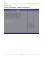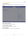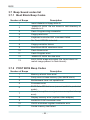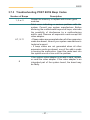
1
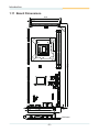
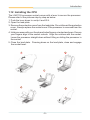
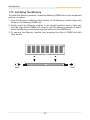
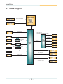
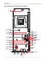
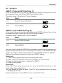
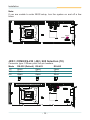
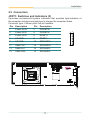
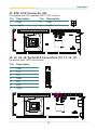
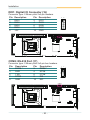
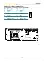
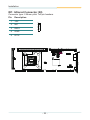
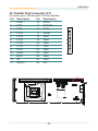
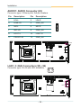
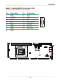
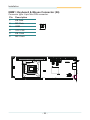
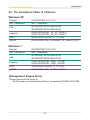
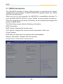
HC67Q2
PICMG 1.3 Full-size SBC
User’s Manual
Version 1.0
2011.08
This page is intentionally left blank.
Index
Contents
Chapter 1 - Introduction.......................................................................1
1.1 Copyright Notice................................................................2
1.2 Declaration of Conformity.................................................2
1.3 About This User’s Manual.................................................3
1.4 Warning...............................................................................3
1.5 Replacing the Lithium Battery..........................................4
1.6 Technical Support..............................................................4
1.7 Warranty..............................................................................4
1.8 Packing List........................................................................5
1.9 Ordering Information.........................................................6
1.10 Specifications...................................................................7
1.11 Board Dimensions............................................................8
1.12 Installing the CPU............................................................9
1.13 Installing the Memory....................................................10
Chapter 2 - Installation....................................................................... 11
2.1
2.2
2.3
2.4
Block Diagram .................................................................12
Jumpers and Connectors................................................13
Jumpers & Connectors Location....................................14
Jumpers............................................................................15
JBAT1: Protected RTS Setting ....................................15
JBAT2: Clear CMOS Setting ........................................15
JRS1: COM2 RS-232 / 422 / 485 Selection...................16
2.5 Connectors.......................................................................17
JFRT1: Switches and Indicators..................................17
JUSB1~5: USB Ports.....................................................18
JFAN1, 2: Fan Connectors ..........................................18
J7: ATX +12V Connector...............................................19
J2, J3, J5, J6: Serial ATA Connectors..........................19
DIO1: Digital I/O Connector..........................................20
COM2: RS-232 Port . .....................................................20
COM1: RS-232/422/485 Port . .......................................21
IR1: Infrared Connector.................................................22
J4: Parallel Port Connector...........................................23
AUDIO1: AUDIO Connector...........................................24
LAN1, 2: GbE Connectors.............................................24
VGA1: Analog RBG Connector.....................................25
KBM1: Keyboard & Mouse Connector.........................26
2.6 The Installation Paths of CD Driver................................27
-I-
Index
Chapter 3 - BIOS.................................................................................29
3.1 BIOS Introduction............................................................30
3.2 Advanced Settings...........................................................32
3.2.1 ACPI Settings........................................................33
3.2.2 CPU Configuration................................................34
3.2.3 SATA Configuration..............................................36
3.2.4 Intel® IGD SWSCI OpRegion................................37
3.2.5 Intel® Trusted Execution Technology
Configuration........................................................38
3.2.6 USB Configuration................................................39
3.2.7 Super IO Configuration........................................40
Serial Port 1 Configuration.....................................41
Serial Port 2 Configuration.....................................42
Parallel Port Configuration.....................................43
3.2.8 H/W Monitor...........................................................44
3.3 Advanced Chipset Settings.............................................45
3.3.1 North Bridge..........................................................46
3.3.2 South Bridge........................................................47
PCI Express Ports Configuration...........................48
USB Configuration...................................................49
3.3.3 ME Subsystem.....................................................50
Integrated Clock Chip Configuration.....................51
3.4 Boot Settings....................................................................52
3.5 Security.............................................................................54
3.6 Exit Options......................................................................55
3.7 Beep Sound codes list.....................................................56
3.7.1 Boot Block Beep Codes.....................................56
3.7.2 POST BIOS Beep Codes....................................56
3.7.3 Troubleshooting POST BIOS Beep Codes.......57
3.8 AMI BIOS Checkpoints....................................................58
3.8.1 Bootblock Initialization Code Checkpoints......58
3.8.2 Bootblock Recovery Code Checkpoints..........60
3.8.3 POST Code Checkpoints...................................62
3.8.4 DIM Code Checkpoints.......................................66
3.8.5 ACPI Runtime Checkpoints...............................67
Appendix.............................................................................................69
Appendix A: I/O Port Address Map.......................................70
Appendix B: BIOS Memory Map...........................................72
Appendix C: Interrupt Request Lines (IRQ).........................74
Appendix D: Digital I/O Setting.............................................75
Appendix E: Watchdog Timer (WDT) Setting.......................81
- II -
Introduction
1
Chapter 1
Introduction
Chapter 1 - Introduction
-1-
Introduction
1.1 Copyright Notice
All Rights Reserved.
The information in this document is subject to change without prior notice in
order to improve the reliability, design and function. It does not represent a
commitment on the part of the manufacturer.
Under no circumstances will the manufacturer be liable for any direct, indirect,
special, incidental, or consequential damages arising from the use or inability
to use the product or documentation, even if advised of the possibility of such
damages.
This document contains proprietary information protected by copyright.
All rights are reserved. No part of this manual may be reproduced by any
mechanical, electronic, or other means in any form without prior written
permission of the manufacturer.
1.2 Declaration of Conformity
CE
This product has passed the CE test for environmental specifications when
shielded cables are used for external wiring. This kind of cable is available
from ICI. Please contact your local supplier for ordering information.
Test conditions for passing included the equipment being operated within an
industrial enclosure. In order to protect the product from being damaged by
ESD (Electrostatic Discharge) and EMI leakage, we strongly recommend the
use of CE-compliant industrial enclosure products.
FCC Class A
This device complies with Part 15 of the FCC Rules. Operation is subject
to the following two conditions : (1) this device may not cause harmful
interference, and (2) this device must accept any interference received,
including interference that may cause undesired operation.
ROHS
Industrial Computers Inc. certifies that all components in its products are
in compliance and conform to the European Union’s Restriction of Use of
Hazardous Substances in Electrical and Electronic Equipment (RoHS) Directive
2002/95/EC.
The above mentioned directive was published on 2/13/2003. The main
purpose of the directive is to prohibit the use of lead, mercury, cadmium,
hexavalent chromium, polybrominated biphenyls (PBB), and polybrominated
diphenyl ethers (PBDE) in electrical and electronic products. Member states of
-2-
Introduction
the EU are to enforce by 7/1/2006.
Industrial Computers Inc. hereby states that the listed products do not
contain unintentional additions of lead, mercury, hex chrome, PBB or PBDB that
exceed a maximum concentration value of 0.1% by weight or for cadmium
exceed 0.01% by weight, per homogenous material. Homogenous
material is defined as a substance or mixture of substances with uniform
composition (such as solders, resins, plating, etc.). Lead-free solder is used for all
terminations (Sn(96-96.5%), Ag(3.0-3.5%) and Cu(0.5%)).
SVHC / REACH
To minimize the environmental impact and take more responsibility to the
earth we live, Arbor hereby confirms all products comply with the restriction
of SVHC (Substances of Very High Concern) in (EC) 1907/2006 (REACH
--Registration, Evaluation, Authorization, and Restriction of Chemicals)
regulated by the European Union.
All substances listed in SVHC < 0.1 % by weight (1000 ppm)
1.3 About This User’s Manual
This user’s manual provides general information and installation instructions
about the product. This User’s Manual is intended for experienced users and
integrators with hardware knowledge of personal computers. If you are not
sure about any description in this booklet. Please consult your vendor before
further handling.
1.4 Warning
Single Board Computers and their components contain very delicate
Integrated Circuits (IC). To protect the Single Board Computer and its
components against damage from static electricity, you should always follow
the following precautions when handling it :
1. Disconnect your Single Board Computer from the power source when you
want to work on the inside.
2. Hold the board by the edges and try not to touch the IC chips, leads or
circuitry.
3. Use a grounded wrist strap when handling computer components.
4. Place components on a grounded antistatic pad or on the bag that comes
with the Single Board Computer, whenever components are separated
from the system.
-3-
Introduction
1.5 Replacing the Lithium Battery
Incorrect replacement of the lithium battery may lead to a risk of explosion.
The lithium battery must be replaced with an identical battery or a battery type
recommended by the manufacturer.
Do not throw lithium batteries into the trash-can. It must be disposed of in
accordance with local regulations concerning special waste.
1.6 Technical Support
If you have any technical difficulties, please do not hesitate to call or e-mail our
customer service.
http://www.eindustrialcomputers.com
email: [email protected]
1.7 Warranty
This product is warranted to be in good working order for a period of two years
from the date of purchase. Should this product fail to be in good working order
at any time during this period, we will, at our option, replace or repair it at no
additional charge except as set forth in the following terms. This warranty does
not apply to products damaged by misuse, modifications, accident or disaster.
Vendor assumes no liability for any damages, lost profits, lost savings or any
other incidental or consequential damage resulting from the use, misuse of,
or inability to use this product. Vendor will not be liable for any claim made by
any other related party.
Vendors disclaim all other warranties, either expressed or implied, including
but not limited to implied warranties of merchantability and fitness for a
particular purpose, with respect to the hardware, the accompanying product’s
manual(s) and written materials, and any accompanying hardware. This limited
warranty gives you specific legal rights.
Return authorization must be obtained from the vendor before returned
merchandise will be accepted. Authorization can be obtained by calling or
faxing the vendor and requesting a Return Merchandise Authorization (RMA)
number. Returned goods should always be accompanied by a clear problem
description.
-4-
Introduction
1.8 Packing List
Packing List
Before you begin installing your single board, please make sure that the following
materials have been shipped:
1 x HC67Q2 PICMG 1.3 Full-size SBC
1 x Driver CD
1 x Quick Installation Guide
Cable Kit
CBK-06-67Q1-00
1 x RS-232 cable
1 x RS-232/422/485 cable
1 x SATA cable
1 x USB cable w/ bracket
1 x Keyboard & Mouse cable
1 x AUDIO cable
If any of the above items is damaged or missing, contact your vendor
immediately.
-5-
Introduction
1.9 Ordering Information
Note:
HC67Q2 supports 4 x PCIe x1 Slots. Another version is available that supports 1 x x4 PCIe x4 slot
PCIe x4 slot and PCIe x1 slot can’t work at the same time with the same BIOS
version. Therefore, 2 BIOS versions are required to be applied as following
configurations. If you want to change the BIOS setting for PCIe support, please
contact our tech support at [email protected]
Update BIOS in DOS:
- PCIex1.bat: BIOS set as PCIe x1 enabled.
- PCIex4.bat: BIOS set as PCIe x4 enabled.
-6-
Introduction
1.10 Specifications
Form Factor
PICMG 1.3 Full-size SBC
Processor
Socket LGA1155 for Intel 32nm Sandy Bridge
processors (i7-2600 at 3.4GHz, i5-2400 at 3.1GHz,
i3-2120 at 3.3GHz, or Pentium G850 at 2.9GHz)
Chipset
Intel® PCH Q67
System Memory
Graphics
Display
Super I/O
2 x 240-pin Long-DIMM sockets, supporting DDR3
1066/1333MHz, up to 8GB
Integrated Intel HD Graphics 200
1 x Analog RGB supported, up to 2048 x 1536 @60Hz
Fintek F71869ED
BIOS
AMI BIOS
2 x SATA 600MB/s ports,
4 x SATA 300MB/s ports (2 x SATA ports on SBC,
Serial ATA
2 x SATA ports through GF to Backplane)
Support RAID 0, 1, 5, 10
Ethernet
2 x Intel 82583V PCIe GbE controllers
14 x USB 2.0 ports: 10 x ports by pin-header, 4 x ports
USB 2.0
to GF
2 x COM ports: COM1 RS-232, COM2 RS-232/422/485
Serial Port
selectable
Parallel Port
SPP/EPP/ECP mode
Digital I/O
8-bit programmable digital I/O
Keyboard/
One 6-pin Mini-DIN connector for keyboard and mouse
Mouse
(PS/2 standard via Y-cable)
Audio
HD Audio Codec ALC886, Line-in/ Line-out/MIC
Expansion Bus
Standard SHB Express
Power Connector 4-pin ATX 12V type and ATX feature
Certification
CE/FCC
Operation Temp. 0oC ~ 60oC (32oF ~ 140oF)
Humidity
0% ~ 95% non-condensing
Dimension (L x W) 338 x 126 mm (13.3" x 4.96")
-7-
Introduction
1.11 Board Dimensions
118.00
108.77
3
.2
Ø3
4
4.12
8.0
xØ
1
4
338.60
329.58
2
+
9
10
+
9
10
2
1
1
2
9
10
9
10
10
9
1
2
5
6
2
1
2
25
26
1
1
9
9
2
10
5
6
1
20
2
3
1
2
1
5
4
6
10
11
4.00
92.2
12
11
15
3.44
1
2
10
1
2
16
15
1
19
126.4
Unit:mm
-8-
Introduction
1.12 Installing the CPU
The LGA1155 processor socket comes with a lever to secure the processor.
Please refer to the pictures step by step as below.
1. Push the lever down to unclip it and lift it.
2. Open the load plate.
3. Remove the protective cover from the load plate. Do not discard the protective
cover. Always replace the socket cover if the processor is removed from the
socket.
4. Hold processor with your thumb and index fingers, oriented as shown. Ensure
your fingers align to the socket cutouts. Align the notches with the socket.
Lower the processor straight down without tilting or sliding the processor in
the socket.
5. Close the load plate. Pressing down on the load plate, close and engage
the socket lever.
2
1
3
4
5
-9-
Introduction
1.13 Installing the Memory
To install the Memory module, locate the Memory DIMM slot on the board and
perform as below:
1. Hold the Memory module so that the key of the Memory module align with
those on the Memory DIMM slot.
2. Gently push the Memory module in an upright position and a right way
until the clips of the DIMM slot close to lock the Memory module in place,
when the Memory module touches the bottom of the DIMM slot.
3. To remove the Memory module, just pressing the clips of DIMM slot with
both hands.
Lock
Lock
- 10 -
Installation
2
Chapter 2
Installation
Chapter 2 - Installation
- 11 -
Installation
2.1 Block Diagram
Dual Channel DDR3
2 x 240-pin DDR3
DIMM socket
1066/1333 MT/z
PCIex16 I/F
PICMG 1.3
PCIex16 GF
Socket LGA1155
for Intel®
i3-2120/
i5-2400/
i7-2600
Processor
FDI
Analog R.G.B.
VGA
USB ports
1 x RJ-45
BIOS
4 x SATA
COM1 RS-232,
COM2 RS-232/422/485 selectable
COM1~2
COM1~2
10 x USB 2.0 ports
KB, MS
ALC886
7.1 Channel
Line-in/out, MIC
1 x RJ-45
DMI
(x4)
GbE
GbE
82583V GbE
Controller
82583V GbE
Controller
HD Audio
Link
PCIex1
LPC I/F
Intel®
Q67
PCH
Fintek
F71869ED
Super I/O
Parallel Port
LPT 2*13
IrDA
IrDA
8-bit Digital I/O
PCIex1
Digital I/O
Serial ATA I/F
PICMG 1.3
SATA GF
4 x USB ports
PICMG 1.3
USB GF
4 x PCI Masters
PICMG 1.3
PCI GF
4 x PCIex1 Lanes
PICMG 1.3
PCIe GF
SPI
Serial ATA I/F
- 12 -
PS/2 KB/ MS
Installation
2.2 Jumpers and Connectors
Jumpers/ Connectors Quick Reference
Jumpers
Label
Description
JBAT1
Protected RTC Setting
JBAT2
Clear CMOS Setting
JRS1
COM2 RS-232/422/485 Selection
Connectors
Label
AUDIO1
COM1
COM2
DIO1
IR1
J2, J3, J5, J6
J4
J7
JFAN1~2
JFRT1
JUSB1~5
KBM1
LAN1~2
VGA1
Description
AUDIO Connector
RS-232 Connector
RS-232/422/485 Connector
Digital I/O Connector
Infrared Connector
SATA Connectors
LPT Connector
ATX1 2V power Connector
Fan Connectors
Switches and Indicators
USB Port Connectors
Keyboard and Mouse Connector
Ethernet Connectors
Analog RGB Connector
- 13 -
Installation
2.3 Jumpers & Connectors Location
1
3
2
4
J7 10
Socket
LGA1155
JFAN2 9
11 JFAN1
JUSB3 8
JUSB1 7
12 J5
1
1
2
1
1
9
10
10
9
1
2
1
2
JUSB2 6
14 J6
15 J3
16 DIO1
17 COM2
18 JRS1
1
9
10
10
9
10
9
1
2
JUSB5 5
5
6
JUSB4 4
19 COM1
JFRT1 3
JBAT2 2
13 J2
1
2
1
1
1
15
2
20 IR1
16
21 J4
JBAT1 1
1
2
11
12
25
26
25
KBM1 VGA1
23
LAN1
24
LAN2
- 14 -
26
22 AUDIO1
Installation
2.4 Jumpers
JBAT1: Protected RTS Setting (1)
If the board refuses to boot due to inappropriate CMOS settings here is how
to proceed to clear (reset) the CMOS to its default values.
Connector type: 2.54mm pitch 1x3-pin headers
Pin
Mode
1-2
Keep Protected (Default)
2-3
Clear CMOS
1
2 3
1
2
3
JBAT2: Clear CMOS Setting (2)
If the board refuses to boot due to inappropriate CMOS settings here is how
to proceed to clear (reset) the CMOS to its default values.
Connector type: 2.54mm pitch 1x3-pin headers
Pin
Mode
1-2
Keep CMOS (Default)
2-3
Clear CMOS
1
2 3
1
2
3
You may need to clear the CMOS if your system cannot boot up because you
forgot your password, the CPU clock setup is incorrect, or the CMOS settings
need to be reset to default values after the system BIOS has been updated.
Refer to the following solutions to reset your CMOS setting:
Solution A:
1. Power off the system and disconnect the power cable.
2. Place a shunt to short pin 2 and pin 3 of JBAT1 for five seconds.
3. Place the shunt back to pin 1 and pin 2 of JBAT1.
4. Power on the system.
Solution B:
If the CPU Clock setup is incorrect, you may not be able to boot up. In this
case, follow these instructions:
Turn the system off, then on again. The CPU will automatically boot up using
standard parameters.
As the system boots, enter BIOS and set up the CPU clock.
- 15 -
Installation
1
2
5
16
6
2
10
10
2
11
1
1
2
12
1
25
1
1
1
2
26
Note:
If you are unable to enter BIOS setup, turn the system on and off a few
times.
2
1
1
9
15
9
10
10
1
9
9
10
2
1
1
3
Socket
LGA1155
2
4
9
1
1
JBAT1
JBAT2
JRS1: COM2 RS-232 / 422 / 485 Selection (18)
2
1
2
1
2
5
6
5
6
5
6
10
6
5
2
1
9
15
1
9
10
10
9
1
9
10
2
9
1
1
Socket
LGA1155
1
3
2
4
1
- 16 -
2
12
1
11
JRS1
16
2
10
2
2
1
1
1
25
1
1
1
2
1
26
Connector type: 2.00mm pitch 2x3-pin headers.
Mode RS-232 (Default) RS-422
RS-485
1-2
Short
Open
Open
3-4
Open
Short
Open
5-6
Open
Open
Short
Installation
2.5 Connectors
JFRT1: Switches and Indicators (3)
It provides connectors for system indicators that provides light indication of
the computer activities and switches to change the computer status.
Connector type: 2.54mm pitch 2x8-pin headers.
Pin
Description
Pin
Description
1
Power LED+
2
PWRBTN+
3
Power LED-
4
PWRBTN-
5
Power LED-
6
RESET+
7
HD LED+
8
RESET-
9
HD LED-
10
SPEAKER+
11
SMB CLK
12
SPEAKER+
13
SMB DAT
14
SPEAKER-
15
SMB GND
16
SPEAKER-
1 2
6
5
2
16
10
2
2
10
2
1
9
10
9
JFRT1
1
9
10
2
9
1
1
Socket
LGA1155
1
3
2
4
1
15
1
9
10
- 17 -
2
12
1
11
1
1
1
25
1
1
1
2
26
15 16
Installation
JUSB1~5: USB Ports (4, 5, 6, 7, 8)
5
16
6
2
10
2
2
10
2
1
1
1
JUSB2
JUSB3
JUSB1
11
2
12
1
25
1
1
1
2
26
Connector type: 2.54mm pitch 2x5 pin-header, pin-10 is eliminated.
Pin Description.
Pin Description.
1 2
1
+5V
2
+5V
3
USBD14
USBD25
USBD+
6
USBD2+
7
GND
8
GND
9 10
9
N/C (Key)
10
N/C
1
1
9
9
10
2
1
1
1
1
3
Socket
LGA1155
2
4
9
JUSB4
JUSB5
1
9
10
15
9
10
JFAN1, 2: Fan Connectors (9), (11)
Connector type: 2.54mm pitch 1x4-pin wafer connector.
Pin
Description
1
GND
2
1
2
+12V
3
4
3
RPM
4
FAN_CTL
6
5
2
16
10
2
2
10
2
1
9
15
1
9
10
10
9
1
9
10
2
9
1
JFAN2
1
Socket
LGA1155
1
3
2
4
1
- 18 -
2
12
1
11
1
1
1
25
1
1
1
2
26
JFAN1
Installation
J7: ATX +12V Connector (10)
J7 supplies the CPU operation ATX +12V (Vcore).
Pin
Description
GND
2
GND
3
+12V
4
+12V
1
2
3
4
26
Description
1
2
5
2
12
1
16
6
2
10
10
2
11
1
1
1
25
1
1
1
2
Pin
2
1
1
9
15
9
10
10
1
9
9
10
2
1
9
2
4
1
1
1
3
Socket
LGA1155
J7
J2, J3, J5, J6: Serial ATA Connectors (12, 13, 14, 15)
Connector type: SATA connectors.
Pin
Description
1
GND
2
TX+
3
TX-
4
GND
5
RX-
6
RX+
7
GND
1
7
26
J3
9
2
10
6
5
2
16
J6
1
1
9
15
10
2
2
10
10
9
1
9
10
2
9
1
1
Socket
LGA1155
1
3
2
4
1
- 19 -
2
12
1
11
1
J5
1
1
25
1
1
1
2
J2
Installation
DIO1: Digital I/O Connector (16)
1
2
10
2
12
1
2
5
16
6
2
10
10
2
11
DIO1
1
1
1
25
1
1
1
2
9
26
Connector type: 2.54mm pitch 2x5-pin headers.
Pin Description
Pin Description
1
DIO0
2
DIO1
3
DIO2
4
DIO3
5
DIO4
6
DIO5
7
DIO6
8
DIO7
9
+5V
10 GND
2
1
1
9
15
9
10
10
1
9
9
10
2
1
1
1
Socket
LGA1155
1
3
2
4
9
COM2: RS-232 Port (17)
Connector type: 2.54mm pitch 2x5-pin box headers.
Pin Description
Pin Description
1
DCD#
2
DSR#
3
RXD
4
RTS#
5
TXD
6
CTS#
7
DTR#
8
RI#
9
GND
10
N/C
1
9
2
10
6
5
2
16
10
2
2
10
2
1
9
15
1
9
10
10
9
1
9
10
2
9
1
1
Socket
LGA1155
1
3
2
4
1
- 20 -
2
12
1
11
1
1
1
25
1
1
1
2
26
COM2
Installation
COM1: RS-232/422/485 Port (19)
Connector type: 2.54mm pitch 2x7-pin box headers.
Pin
Description
Pin
Description
1
DCD#
2
DSR#
3
RXD
4
RTS#
5
TXD
6
CTS#
7
DTR#
8
RI#
9
GND
10
GND
11
442TX+/ 485+
12
422TX-/ 485-
13
422RX+
14
422RX-
1 2
13 14
6
5
2
16
10
2
2
10
2
1
9
15
1
9
10
10
9
1
9
10
2
9
1
1
Socket
LGA1155
1
3
2
4
1
- 21 -
2
12
1
11
1
1
1
25
1
1
1
2
26
COM1
Installation
IR1: Infrared Connector (20)
Connector type: 2.54mm pitch 1x5-pin headers.
Description
+5V
2
N/C
3
IRRX
4
GND
5
IRTX
1
2
3
4
5
6
5
2
1
IR1
9
1
9
16
10
15
2
10
2
2
10
10
9
1
9
10
2
9
1
1
Socket
LGA1155
1
3
2
4
1
- 22 -
2
12
1
11
1
1
1
25
1
1
1
2
1
26
Pin
Installation
J4: Parallel Port Connector (21)
Connector type: 2.54mm pitch 2x13 box headers.
Pin
Description
Pin
Description
1
STB#
14
AFD#
2
PTD0
15
ERROR#
3
PTD1
16
INIT#
4
PTD2
17
SLIN#
5
PTD3
18
GND
6
PTD4
19
GND
7
PTD5
20
GND
8
PTD6
21
GND
9
PTD7
22
GND
10
ACK#
23
GND
11
BUSY
24
GND
12
PE
25
GND
13
SELECT
26
N/C
1 14
13 26
6
5
2
16
10
2
2
10
2
1
9
15
1
9
10
10
9
1
9
10
2
9
1
1
Socket
LGA1155
1
3
2
4
1
- 23 -
2
12
1
11
1
1
1
25
1
1
1
2
26
J4
Installation
AUDIO1: AUDIO Connector (22)
Connector type: 2.00mm pitch 2x6-pin headers.
Pin
Description
Pin
Description
1
LIN-L
2
LIN-R
3
LINE-JD
4
GND_AU
5
MICL
6
MICR
7
MIC-JD
8
GND_AU
9
LOUT-L
10
LOUT-R
11
FRONT-JD
12
GND_AU
1
2
2
26
25
1
1
1
1
11 12
2
12
1
11
1
16
5
2
1
AUDIO1
6
2
10
10
2
2
1
1
9
15
9
10
10
1
9
9
10
2
1
1
1
Socket
LGA1155
1
3
2
4
9
LAN1, 2: GbE Connectors (23), (24)
6
5
2
16
10
2
2
10
2
1
9
15
1
9
10
10
9
1
9
10
2
9
LAN1
Socket
LGA1155
1
LAN2
1
1
3
2
4
1
- 24 -
2
12
1
11
1
1
1
25
1
1
1
2
26
Connector type: RJ-45 with LED indicators.
Installation
VGA1: Analog RBG Connector (25)
Description
Pin
Description
1
RED
9
VCC
2
GREEN
10
GND
3
BLUE
11
N/C
4
N/C
12
DDC_DATA
5
GND
13
HSYNC
6
GND
14
VSYNC
7
GND
15
DDC-CLK
8
GND
1
11
5
15
16
15
2
12
1
6
5
2
2
10
1
2
10
2
11
1
1
1
25
1
1
1
2
Pin
26
Connector type: D-Sub 15-pin female.
1
9
9
10
10
9
1
9
10
2
9
Socket
LGA1155
1
VGA1
1
1
3
2
4
1
- 25 -
Installation
KBM1: Keyboard & Mouse Connector (26)
Connector type: 6-pin Mini-DIN connector.
Pin
Description
1
KB Data
2
MS Data
6
5
4
3
GND
4
VCC PS2
5
KB Clock
6
MS Clock
3
6
5
2
16
10
2
2
10
2
1
9
15
1
9
10
10
9
1
9
10
2
9
1
1
Socket
LGA1155
1
3
2
4
1
KBM1
- 26 -
2
12
1
11
1
1
1
25
1
1
1
2
26
2 1
Installation
2.6 The Installation Paths of CD Driver
Windows XP
Chipset
\CHIPSET\INF 9.2.0.1021
NET Framework
\NET Framework
LAN
\ETHERNET\INTEL\82583V\32
\ETHERNET\INTEL\82583V\64
Graphics
\GRAPHICS\INTEL_2K_XP_32\5313
\GRAPHICS\INTEL_2K_XP_64\5313
AHCI
\RAID\INTEL\6-series 10.1.0.1008
AUDIO
\AUDIO\REALTEK_HD\WIN2K_XP_x86x64_R257
Windows 7
Chipset
\CHIPSET\INF 9.2.0.1021
NET Framework
\NET Framework
LAN
\ETHERNET\INTEL\82583V\32
\ETHERNET\INTEL\82583V\64
Graphics
\GRAPHICS\INTEL_WIN7_32\2291
\GRAPHICS\INTEL_WIN7_64\2291
AHCI
\RAID\INTEL\6-series 10.1.0.1008
AUDIO
\AUDIO\REALTEK_HD\Win7_R257
Management Engine Driver
Please download the driver at:
ftp://ftp.arbor.com.tw/pub/driver/01slot_computing/HiCORE-i67Q1/ME/
- 27 -
This page is intentionally left blank.
BIOS
3
Chapter 3
BIOS
Chapter 3 - BIOS
- 29 -
BIOS
3.1 BIOS Introduction
The AMI BIOS provides a Setup utility program for specifying the system
configurations and settings. The BIOS ROM of the system stores the Setup
utility and configurations.
When you turn on the computer, the AMI BIOS is immediately activated. To
enter the BIOS SETUP UTILILTY, press “Delete” once the power is turned on.
When the computer is shut down, the battery on the motherboard supplies the
power for BIOS RAM.
The Main Setup screen lists the following information
BIOS Information
BIOS Vendor: displays the vendor name
Core Version: displays the current version information of the core
Project Version
Build Date: the date when the project was made/updated
Memory Information: displays the total memory
Access Level: shows user’s access level
- 30 -
BIOS
Key Commands
BIOS Setup Utility is mainly a key-based navigation interface. Please refer to
the following key command instructions for navigation process.
“←”“→”
Move to highlight a particular configuration screen from
the top menu bar / Move to highlight items on the screen
“↓” “↑”
Move to highlight previous/next item
Enter
Select and access a setup item/field
Esc
On the Main Menu – Quit the setup and discard changes
saved into CMOS (a message screen will display and ask
you to select “OK” or “Cancel” for exiting and discarding
changes. Use “←” and “→” to select and press “Enter” to
confirm)
On the Sub Menu – Exit current page and return to main
menu
Page Up / +
Increase the numeric value on a selected setup item /
make change
Page Down -
Decrease the numeric value on a selected setup item /
make change
F2
Recover to previous values in setup
F3
Recover to optimized defaults automatically
F1
Activate “General Help” screen
F10
Save the changes that have been made in the setup and
exit. (a message screen will display and ask you to select
“OK” or “Cancel” for exiting and saving changes. Use “←”
and “→” to select and press “Enter” to confirm)
System Date
Set the system date. Note that the “Day” automatically changes when you
set the date.
The date format is:
Day : Sun to Sat
Month : 1 to 12
Date : 1 to 31
Year : 1999 to 2099
System Time
Set the system time.
The time format is:
Hour : 00 to 23
Minute : 00 to 59
Second : 00 to 59
- 31 -
BIOS
3.2 Advanced Settings
The “Advanced” screen provides setting options to configure ACPI, CPU,
SATA, USB, Super IO and other peripherals. You can use “←” and “→” keys
to select “Advanced” and use the “↓” and “↑” to select a setup item.
Note:
Please pay attention to the instructions at the upper-right frame before you
decide to configure any setting of an item.
- 32 -
BIOS
3.2.1 ACPI Settings
Press “Enter” on “ACPI Settings” and you will be able to set up ACPI
configuration.
Enable ACPI Auto Configuration
Allow you to enable or disable BIOS ACPI Auto Configuration.
Enable Hibernation
Allow you to enable or disable system hibernation (OS/S4 Sleep State).
This option may not be effective in some OSes.
ACPI Sleep State
Provide 3 options, Suspend Disable, S1 (CUP Stop Clock), and S3 (Suspend
to RAM) in order. Suspend ranks the highest ACPI sleep state.
Lock Legacy Resources
Allow you to enable or disable Lock Legacy Resources.
- 33 -
BIOS
3.2.2 CPU Configuration
Press “Enter” on “CPU Configuration” to configure the CPU on the “CPU
Configuration” screen.
CPU Details
Detail information including CPU manufacturer name, Processor Speed,
Processor Stepping, Microcode Revision, Processor Core number, etc.
Hyper-Threading Technology
Enabled: activates the Hyper-Threading Technology for higher CPU threading
speed. (Recommended)
Disabled: deactivates the Hyper-Threading Technology.
- 34 -
BIOS
Active Processor Cores
Number of cores to enable in each processor package.
The choice: All, 1, 2
Limit CPUID Maximum
Disable for Windows XP.
The choice: Disabled, Enabled
Execute Disable Bit
Enable/Disbale the Execute disable bit function.
Hardware Prefetcher
To turn on/off the MLC streamer prefetcher.
The choice: Disabled, Enabled
Adjacent Cache Line Prefetch
To turn on/off prefetching of adjacent cache lines.
The choice: Disabled, Enabled
Intel® Virtualization Technology
Enable/Disbale the Intel® Virtualization Technology feature.
Power Technology
Enable the power management features.
The choice: Disabled, Energy Efficient, Custom
- 35 -
BIOS
3.2.3 SATA Configuration
SATA Mode
It allows you to select the operation mode for SATA controller.
Serial-ATA Controller 0
Enable/ Disable Serial ATA Controller 0.
The choice: Disable, Enhanced, Compatible
Serial-ATA Controller 1
Enable/ Disable Serial ATA Controller 0.
The choice: Disable, Enhanced
- 36 -
BIOS
3.2.4 Intel® IGD SWSCI OpRegion
DVMT/ Fixed Memory
This feature allows you to select the memory size of DVMT/BOTH operating
mode.
The choice: 256MB, 128MB, Maximum
IGD – Boot Type
This feature allows you to select the display device when you boot up the
system.
- 37 -
BIOS
3.2.5 Intel® Trusted Execution Technology Configuration
The menu is used to read USB configuration information and configure the
USB setting.
Intel® TXT(LT) Support
This item allows you to enable/disable the Intel TXT (LT) support.
- 38 -
BIOS
3.2.6 USB Configuration
The menu is used to read USB configuration information and configure the
USB setting.
Legacy USB Support
Enable support for legacy USB. Normally if this option is not enabled, any
attached USB mouse or USB keyboard won’t be accessible until a USB
compatible operating system is fully booted with all loaded USB drivers. When
this option is enabled, any attached USB mouse or USB keyboard can control
the system even when there is no USB driver loaded onto the system.
The choice: Enabled, Disabled, Auto (AUTO option disables legacy support if
no USB devices are connected.)
EHCI Hand-Off
This option allows you to enable EHCI Hand-Off function by BIOS if your
computer operating system does not support it. EHCI is the abbreviation for
Enhanced Host Controller Interface, which is necessary for high speed USB
operation.
The choice: Enabled, Disabled
- 39 -
BIOS
Mass Storage Devices
This item allows you to set up mass storage devices.
The choice: Auto, Floppy, Forced FDD, Hard-Disk, CD-ROM
3.2.7 Super IO Configuration
You can use this item to set up or change the Super IO configuration for FDD
controllers, parallel ports and serial ports.
- 40 -
BIOS
Serial Port 1 Configuration
Serial Port
This item allows you to enable/disable Serial Port (COM).
- 41 -
BIOS
Serial Port 2 Configuration
Serial Port
This item allows you to enable/disable Serial Port (COM).
Change Settings
This item allows you to change the serial port IO port address and interrupt
address.
COMB RS-485 Autoflow
This item allows you to enable serial port 2 auto flow control function.
Auto flow control is used in RS-485 to control the signal transmitter
automatically. When RS-485 auto flow is disabled, the RS-485 auto flow will
not work. RS-422/485 is available after modifying the COMB RS-485 Autoflow
in BIOS setting to enabled.
The choice: Enabled, Disabled (default)
- 42 -
BIOS
Parallel Port Configuration
Parallel Port Configuration
This item allows you to enable/disable Parallel Port (LPT/LPTE).
- 43 -
BIOS
3.2.8 H/W Monitor
The H/W Monitor lists out the temperature, fan speeds and system voltages
that is being monitored.
FAN1 Mode Setting
Allow you to select the FAN control mode.
FAN2 Mode Setting
Allow you to select the FAN control mode.
CPU/System Temperature
Show you the current CPU/System fan temperature.
System FAN1/2 Speed
Show you the current system Fan operating speed.
Vcore
Show you the voltage level of CPU (Vcore).
- 44 -
BIOS
+3.3V / +5V / VBAT
Show you the voltage level of the +3.3V, +5V standby and battery.
VDIMM
Show you the current VDIMM voltage.
3.3 Advanced Chipset Settings
Select “Chipset” to enable CRID, access “North Bridge,” “South Bridge” and
“ME Subsystem.”
- 45 -
BIOS
3.3.1 North Bridge
Vt-d
Enable/Disable the Vt-d function.
Initate Graphic Adapter
This item allows you to select which graphics controller to use and set it as the
primary boot device.
The choice: IGD, PCI/IGD, PCI/PEG, PEG/IGD, PEG/PCI
IGD Memory
This item shows the information of the IGD (Internal Graphics Device) memory.
- 46 -
BIOS
3.3.2 South Bridge
Normally, the south bridge controls the basic I/O functions, such as USB and
audio. This screen allows you to access the configurations of I/Os.
SMBus Controller
SMBus Controller help
The choice: Enabled, Disabled
Wake on Lan from S5
Wake on Lan from S5 help
The choice: Enabled, Disabled
- 47 -
BIOS
PCI Express Ports Configuration
PCI Express Port 1/2/3/4/5/6/7/8
Enable/Disable the PCI Express Ports in the chipset.
- 48 -
BIOS
USB Configuration
The USB Configuration menu is used to read USB configuration information
and configure the USB settings.
All USB Devices
Use this item to enable or disable all USB devices.
- 49 -
BIOS
3.3.3 ME Subsystem
Use the ME Subsystem menu to configure the Intel® Management Engine
(ME) configuration options.
ME Subsystem
Use the ME Subsystem option to enable or disable the Intel® ME subsystem.
The choice: Enabled, Disabled
End of Post Message
Use the End of Post Message option to enable or disable the end of post message of the ME Subsystem.
The choice: Enabled, Disabled
Execute MEBx
Use the Execute MEBx option to enable or disable the Intel® Management
Engine BIOS extension (MEBx).
The choice: Enabled, Disabled
- 50 -
BIOS
Integrated Clock Chip Configuration
ICC Enable
This item allows you to enable or disable the current ICC.
- 51 -
BIOS
3.4 Boot Settings
Bootup Numlock State
This item determines if the Numlock key is active or inactive at system
start-up time.
Quiet Boot
This item can helps to select screen display when the system boots.
The choice: Enabled, Disabled
Boot Option Priorities
This item allows you to select boot priorities for all boot devices.
- 52 -
BIOS
Boot Option #1
This item allows you to set the system boot priorities.
- 53 -
BIOS
3.5 Security
You can set administrator password by Security menu.
- 54 -
BIOS
3.6 Exit Options
Use the option to exit BIOS settings, and save/discard any changes you
made.
Save Changes and Exit
Exit system setup after saving the changes.
Discard Changes and Exit
Exit system setup without saving any changes.
Discard Changes
Discard changes done so far to any of the setup questions.
- 55 -
BIOS
3.7 Beep Sound codes list
3.7.1 Boot Block Beep Codes
Number of Beeps
Description
1
Insert diskette in floppy drive A:
2
‘AMIBOOT.ROM’ file not found in root directory of
diskette in A:
4
Flash Programming successful
5
Floppy read error
6
Keyboard controller BAT command failed
7
No Flash EPROM detected
8
Floppy controller failure
9
Boot Block BIOS checksum error
10
Flash Erase error
11
Flash Program error
12
‘AMIBOOT.ROM’ file size error
13
BIOS ROM image mismatch (file layout does not
match image present in flash device)
3.7.2 POST BIOS Beep Codes
Number of Beeps
Description
1
Memory refresh timer error.
2
Parity error in base memory (first 64KB block)
4
Motherboard timer not operational
5
8
Processor error
8042 Gate A20 test error (cannot switch to protected
mode)
General exception error (processor exception interrupt
error)
Display memory error (system video adapter)
9
AMIBIOS ROM checksum error
10
CMOS shutdown register read/write error
11
Cache memory test failed
6
7
- 56 -
BIOS
3.7.3 Troubleshooting POST BIOS Beep Codes
Number of Beeps
Description
1, 2 or 3
Reseat the memory, or replace with known good
modules.
4-7, 9-11
Fatal error indicating a serious problem with the
system. Consult your system manufacturer. Before
declaring the motherboard beyond all hope, eliminate
the possibility of interference by a malfunctioning
add-in card. Remove all expansion cards except the
video adapter.
• If beep codes are generated when all other expansion
cards are absent, consult your system manufacturer’s
technical support.
• If beep codes are not generated when all other
expansion cards are absent, one of the add-in cards
is causing the malfunction. Insert the cards back into
the system one at a time until the problem
8
If the system video adapter is an add-in card, replace
or reset the video adapter. If the video adapter is an
integrated part of the system board, the board may
be faulty.
- 57 -
BIOS
3.8 AMI BIOS Checkpoints
3.8.1 Bootblock Initialization Code Checkpoints
The Bootblock initialization code sets up the chipset, memory and other
components before system memory is available. The following table describes
the type of checkpoints that may occur during the bootblock initialization
portion of the BIOS (Note):
Checkpoint
Description
Before D0
If boot block debugger is enabled, CPU cache-as-RAM
functionality is enabled at this point. Stack will be enabled
from this point.
D0
Early Boot Strap Processo (BSP) initialization like microcode
update, frequency and other CPU critical initialization. Early
chipset initialization is done.
D1
Early super I/O initialization is done including RTC and
keyboard controller. Serial port is enabled at this point if
needed for debugging. NMI is disabled. Perform keyboard
controller BAT test. Save power-on CPUID value in scratch
CMOS. Go to flat mode with 4GB limit and GA20 enabled.
D2
Verify the boot block checksum. System will hang here if
checksum is bad.
D3
Disable CACHE before memory detection. Execute full
memory sizing module. If memory sizing module is not
executed, start memory refresh and do memory sizing
in Boot block code. Do additional chipset initialization.
Re-enable CACHE. Verify that flat mode is enabled.
D4
Test base 512KB memory. Adjust policies and cache first
8MB. Set stack.
D5
Bootblock code is copied from ROM to lower system
memory and control is given to it. BIOS now executes out of
RAM. Copy compressed boot block code to memory in right
segments. Copy BIOS from ROM to RAM for faster access.
Perform main BIOS checksum and update recovery status
accordingly.
- 58 -
BIOS
D6
D7
Both key sequence and OEM specific method are checked
to determine if BIOS recovery is forced. If BIOS recovery
is necessary, control flows tocheckpoint E0. See Bootblock
Recovery Code Checkpoints section of document for more
information.
Restore CPUID value back into register. The BootblockRuntime interface module is moved to system memory and
control is given to it. Determine whether to execute serial
flash.
D8
The Runtime module is uncompressed into memory. CPUID
information is stored in memory.
D9
Store the Uncompressed pointer for future use in PMM.
Copying Main BIOS into memory. Leaves all RAM below
1MB Read-Write including E000 and F000 shadow areas
but closing SMRAM.
DA
Restore CPUID value back into register. Give control to BIOS
POST (ExecutePOSTKernel). See POST Code Checkpoints
section of document for more information.
DC
System is waking from ACPI S3 state
E1 - E8
EC - EE
OEM memory detection/configuration error. This range is
reserved for chipset vendors & system manufacturers. The
error associated with this value may be different from one
platform to the next.
- 59 -
BIOS
3.8.2 Bootblock Recovery Code Checkpoints
The Bootblock recovery code gets control when the BIOS determines that
a BIOS recovery needs to occur because the user has forced the update
or the BIOS checksum is corrupt. The following table describes the type of
checkpoints that may occur during the Bootblock recovery portion of the BIOS
(Note)
:
Checkpoint
Description
E0
Initialize the floppy controller in the super I/O. Some interrupt
vectors are initialized. DMA controller is initialized. 8259
interrupt controller is initialized. L1 cache is enabled.
E9
Set up floppy controller and data. Attempt to read from floppy.
EA
Enable ATAPI hardware. Attempt to read from ARMD and ATAPI
CDROM.
EB
Disable ATAPI hardware. Jump back to checkpoint E9.
EF
Read error occurred on media. Jump back to checkpoint EB.
F0
Search for pre-defined recovery file name in root directory.
F1
Recovery file not found.
F2
Start reading FAT table and analyze FAT to find the clusters
occupied by the recovery file.
F3
Start reading the recovery file cluster by cluster.
F5
Disable L1 cache.
FA
Check the validity of the recovery file configuration to the current
configuration of the flash part.
FB
Make flash write enabled through chipset and OEM specific
method. Detect proper flash part. Verify that the found flash
part size equals the recovery file size.
F4
The recovery file size does not equal the found flash part size.
- 60 -
BIOS
FC
Erase the flash part.
FD
Program the flash part.
FF
The flash has been updated successfully. Make flash write
disabled. Disable ATAPI hardware. Restore CPUID value back
into register. Give control to F000 ROM at F000:FFF0h.
- 61 -
BIOS
3.8.3 POST Code Checkpoints
The POST code checkpoints are the largest set of checkpoints during
the BIOS pre-boot process. The following table describes the type of
checkpoints that may occur during the POST portion of the BIOS (Note):
Checkpoint
Description
03
Disable NMI, Parity, video for EGA, and DMA controllers.
Initialize BIOS, POST, Runtime data area. Also initialize BIOS
modules on POST entry and GPNV area. Initialized CMOS as
mentioned in the Kernel Variable "wCMOSFlags."
04
Check CMOS diagnostic byte to determine if battery power
is OK and CMOS checksum is OK. Verify CMOS checksum
manually by reading storage area. If the CMOS checksum is
bad, update CMOS with power-on default values and clear
passwords. Initialize status register A. Initializes data variables
that are based on CMOS setup questions. Initializes both the
8259 compatible PICs in the system
05
Initializes the interrupt controlling hardware (generally PIC)
and interrupt vector table.
06
Do R/W test to CH-2 count reg. Initialize CH-0 as system
timer.Install the POSTINT1Ch handler. Enable IRQ-0 in
PIC for system timer interrupt. Traps INT1Ch vector to
"POSTINT1ChHandlerBlock."
07
Fixes CPU POST interface calling pointer.
08
Initializes the CPU. The BAT test is being done on KBC.
Program the keyboard controller command byte is being done
after Auto detection of KB/MS using AMI KB-5.
C0
Early CPU Init Start -- Disable Cache – Init Local APIC
C1
Set up boot strap processor Information
C2
Set up boot strap processor for POST
C5
Enumerate and set up application processors
C6
Re-enable cache for boot strap processor
- 62 -
BIOS
C7
Early CPU Init Exit
0A
Initializes the 8042 compatible Key Board Controller.
0B
Detects the presence of PS/2 mouse.
0C
Detects the presence of Keyboard in KBC port.
0E
Testing and initialization of different Input Devices. Also, update
the Kernel Variables. Traps the INT09h vector, so that the
POST INT09h handler gets control for IRQ1. Uncompress all
available language, BIOS logo, and Silent logo modules.
13
Early POST initialization of chipset registers.
20
Relocate System Management Interrupt vector for all CPU in
the system.
24
Uncompress and initialize any platform specific BIOS modules.
GPNV is initialized at this checkpoint.
2A
Initializes different devices through DIM. See DIM Code
Checkpoints section of document for more information.
2C
Initializes different devices. Detects and initializes the video
adapter installed in the system that have optional ROMs.
2E
Initializes all the output devices.
31
Allocate memory for ADM module and uncompress it.
Give control to ADM module for initialization. Initialize language
and font modules for ADM. Activate ADM module.
33
Initializes the silent boot module. Set the window for displaying
text information.
37
Displaying sign-on message, CPU information, setup key
message, and any OEM specific information.
- 63 -
BIOS
38
Initializes different devices through DIM. See DIM Code
Checkpoints section of document for more information. USB
controllers are initialized at this point.
39
Initializes DMAC-1 & DMAC-2.
3A
Initialize RTC date/time.
3B
Test for total memory installed in the system. Also, Check for
DEL or ESC keys to limit memory test. Display total memory
in the system.
3C
Mid POST initialization of chipset registers.
40
Detect different devices (Parallel ports, serial ports, and
coprocessor in CPU, … etc.) successfully installed in the
system and update the BDA, EBDA…etc.
52
Updates CMOS memory size from memory found in memory
test. Allocates memory for Extended BIOS Data Area from
base memory. Programming the memory hole or any kind of
implementation that needs an adjustment in system RAM size
if needed.
60
Initializes NUM-LOCK status and programs the KBD typematic
rate.
75
Initialize Int-13 and prepare for IPL detection.
78
Initializes IPL devices controlled by BIOS and option ROMs.
7C
Generate and write contents of ESCD in NVRam.
84
Log errors encountered during POST.
85
Display errors to the user and gets the user response for error.
87
Execute BIOS setup if needed / requested. Check boot
password if installed.
8C
Late POST initialization of chipset registers.
8D
Build ACPI tables (if ACPI is supported)
8E
Program the peripheral parameters. Enable/Disable NMI as
selected
Initialization of system management interrupt by invoking
all handlers. Please note this checkpoint comes right after
checkpoint 20h
Clean-up work needed before booting to OS.
90
A1
- 64 -
BIOS
A2
Takes care of runtime image preparation for different BIOS
modules. Fill the free area in F000h segment with 0FFh.
Initializes the Microsoft IRQ Routing Table. Prepares the
runtime language module. Disables the system configuration
display if needed.
A4
Initialize runtime language module. Display boot option popup
menu.
A7
Displays the system configuration screen if enabled. Initialize
the CPU’s before boot, which includes the programming of the
MTRR’s.
A9
Wait for user input at config display if needed.
AA
Uninstall POST INT1Ch vector and INT09h vector.
AB
Prepare BBS for Int 19 boot. Init MP tables.
AC
End of POST initialization of chipset registers. De-initializes the
ADM module.
B1
Save system context for ACPI. Prepare CPU for OS boot
including final MTRR values.
00
Passes control to OS Loader (typically INT19h).
- 65 -
BIOS
3.8.4 DIM Code Checkpoints
The Device Initialization Manager (DIM) gets control at various times during
BIOS POST to initialize different system busses. The following table describes
the main checkpoints where the DIM module is accessed (Note):
Checkpoint
Description
2A
Initialize different buses and perform the following functions:
Reset, Detect, and Disable (function 0); Static Device
Initialization (function 1); Boot Output Device Initialization
(function 2). Function 0 disables all device nodes, PCI devices,
and PnP ISA cards. It also assigns PCI bus numbers. Function
1 initializes all static devices that include manual configured
onboard peripherals, memory and I/O decode windows in PCIPCI bridges, and noncompliant PCI devices. Static resources
are also reserved. Function 2 searches for and initializes any
PnP, PCI, or AGP video devices.
38
Initialize different buses and perform the following functions:
Boot Input Device Initialization (function 3); IPL Device
Initialization (function 4); General Device Initialization (function
5). Function 3 searches for and configures PCI input devices
and detects if system has standard keyboard controller.
Function 4 searches for and configures all PnP and PCI boot
devices. Function 5 configures all onboard peripherals that are
set to an automatic configuration and configures all remaining
PnP and PCI devices.
While control is in the different functions, additional checkpoints are output to
port 80h as a word value to identify the routines under execution. The low byte
value indicates the main POST Code Checkpoint. The high byte is divided
into two nibbles and contains two fields. The details of the high byte of these
checkpoints are as follows:
HIGH BYTE XY
The upper nibble “X” indicates the function number that is being executed.
“X” can be from 0 to 7.
- 66 -
BIOS
0 = func#0, disable all devices on the BUS concerned.
2 = func#2, output device initialization on the BUS concerned.
3 = func#3, input device initialization on the BUS concerned.
4 = func#4, IPL device initialization on the BUS concerned.
5 = func#5, general device initialization on the BUS concerned.
6 = func#6, error reporting for the BUS concerned.
7 = func#7, add-on ROM initialization for all BUSes.
8 = func#8, BBS ROM initialization for all BUSes.
The lower nibble 'Y' indicates the BUS on which the different routines are
being executed. 'Y' can be from 0 to 5.
0 = Generic DIM (Device Initialization Manager).
1 = On-board System devices.
2 = ISA devices.
3 = EISA devices.
4 = ISA PnP devices.
5 = PCI devices.
3.8.5 ACPI Runtime Checkpoints
ACPI checkpoints are displayed when an ACPI capable operating system
either enters or leaves a sleep state. The following table describes the type of
checkpoints that may occur during ACPI sleep or wake events (Note):
Checkpoint
Description
AC
First ASL check point. Indicates the system is running
in ACPI mode.
AA
System is running in APIC mode.
01, 02, 03, 04, 05 Entering sleep state S1, S2, S3, S4, or S5.
10, 20, 30, 40, 50 Waking from sleep state S1, S2, S3, S4, or S5.
Note:
Please note that checkpoints may differ between different platforms based on
system configuration. Checkpoints may change due to vendor requirements,
system chipset or option ROMs from add-in PCI devices.
- 67 -
This page is intentionally left blank.
Appendix
Appendix
Appendix
- 69 -
Appendix
Appendix A: I/O Port Address Map
Each peripheral device in the system is assigned a set of I/O port addresses
which also becomes the identity of the device.
The following table lists the I/O port addresses used.
Address
Device Description
0x00000000-0x0000000F
Direct memory access controller
0x00000000-0x0000000F
PCI bus
0x00000010-0x0000001F
Motherboard resources
0x00000020-0x00000021
Programmable interrupt controller
0x00000022-0x0000003F
Motherboard resources
0x00000040-0x00000043
System timer
0x00000044-0x0000005F
Motherboard resources
0x00000060-0x00000060
Standard 101/102-Key or Microsoft Natural
PS/2 Keyboard
0x00000061-0x00000061
System speaker
0x00000062-0x00000063
Motherboard resources
0x00000064-0x00000064
Standard 101/102-Key or Microsoft Natural
PS/2 Keyboard
0x00000065-0x0000006F
Motherboard resources
0x00000070-0x00000071
System CMOS/real time clock
0x00000072-0x0000007F
Motherboard resources
0x00000080-0x00000080
Motherboard resources
0x00000081-0x00000083
Direct memory access controller
0x00000084-0x00000086
Motherboard resources
0x00000087-0x00000087
Direct memory access controller
0x00000088-0x00000088
Motherboard resources
0x00000089-0x0000008B
Direct memory access controller
0x0000008C-0x0000008E
Motherboard resources
0x0000008F-0x0000008F
Direct memory access controller
0x00000090-0x0000009F
Motherboard resources
0x000000A0-0x000000A1
Programmable interrupt controller
0x000000A2-0x000000BF
Motherboard resources
- 70 -
Appendix
0x000000C0-0x000000DF Direct memory access controller
0x000000E0-0x000000EF
Motherboard resources
0x000000F0-0x000000FF
Numeric data processor
0x000001F0-0x00000177
ATA Channel 1
0x000001F0-0x000001F7
ATA Channel 0
0x000002F8-0x0000029F
Motherboard resources
0x000002F8-0x000002FF
Communications Port (COM2)
0x00000378-0x00000376
ATA Channel 1
0x00000378-0x0000037F
Printer Port (LPT1)
0x000003B0-0x000003BB Intel(R) HD Graphics Family
0x000003B0-0x000003BB PCI bus
0x000003C0-0x000003DF Intel(R) HD Graphics Family
0x000003E0-0x00000CF7 PCI bus
0x000003F6-0x000003F6
ATA Channel 0
0x000003F8-0x000003FF
Communications Port (COM1)
0x00000400-0x00000453
System board
0x00000454-0x00000457
Motherboard resources
0x00000458-0x0000047F
System board
0x000004D0-0x000004D1 Motherboard resources
0x00000500-0x0000057F
System board
0x0000D000-0x0000FFFF PCI bus
0x00001180-0x0000119F
System board
0x0000D000-0x0000DFFF Intel(R) 6 Series/C200 Series Chipset Family
PCI Express Root Port 3 - 1C14
0x0000E000-0x0000EFFF Intel(R) 6 Series/C200 Series Chipset Family
PCI Express Root Port 2 - 1C12
0x0000F000-0x0000F03F
Intel(R) HD Graphics Family
0x0000F040-0x0000F05F
Intel(R) 6 Series/C200 Series Chipset Family
SMBus Controller - 1C22
0x0000F060-0x0000F06F
Intel(R) 6 Series/C200 Series Chipset Family 2
port Serial ATA Storage Controller - 1C08
- 71 -
Appendix
0x0000F070-0x0000F07F
Intel(R) 6 Series/C200 Series Chipset Family 2
port Serial ATA Storage Controller - 1C08
0x0000F080-0x0000F083
Intel(R) 6 Series/C200 Series Chipset Family 2
port Serial ATA Storage Controller - 1C08
0x0000F090-0x0000F097
Intel(R) 6 Series/C200 Series Chipset Family 2
port Serial ATA Storage Controller - 1C08
0x0000F0A0-0x0000F0A3 Intel(R) 6 Series/C200 Series Chipset Family 2
port Serial ATA Storage Controller - 1C08
0x0000F0B0-0x0000F0B7 Intel(R) 6 Series/C200 Series Chipset Family 2
port Serial ATA Storage Controller - 1C08
0x0000F0C0-0x0000F0CF Intel(R) 6 Series/C200 Series Chipset Family 4
port Serial ATA Storage Controller - 1C00
0x0000F0D0-0x0000F0DF Intel(R) 6 Series/C200 Series Chipset Family 4
port Serial ATA Storage Controller - 1C00
0x0000F120-0x0000F127
Intel(R) Active Management Technology - SOL
(COM3)
0x0000F130-0x0000F13F
Standard Dual Channel PCI IDE Controller
0x0000F140-0x0000F143
Standard Dual Channel PCI IDE Controller
0x0000F150-0x0000F157
Standard Dual Channel PCI IDE Controller
0x0000F160-0x0000F163
Standard Dual Channel PCI IDE Controller
0x0000F170-0x0000F177
Standard Dual Channel PCI IDE Controller
Appendix B: BIOS Memory Map
Address
Device Description
0xFED10000-0xFED19FFF
System board
0xE0000000-0xEFFFFFFF
System board
0xFED90000-0xFED93FFF
System board
0xFED20000-0xFED3FFFF System board
0xFEE00000-0xFEE0FFFF
System board
0xFB400000-0xFB7FFFFF
Intel(R) HD Graphics Family
0xD0000000-0xDFFFFFFF
Intel(R) HD Graphics Family
0xFBC07000-0xFBC07FFF
Intel(R) Active Management Technology SOL (COM3)
- 72 -
Appendix
0xFBC00000-0xFBC03FFF
High Definition Audio Controller
0xFBC04000-0xFBC040FF
Intel(R) 6 Series/C200 Series Chipset Family
SMBus Controller - 1C2
0xFED00000-0xFED003FF
High Precision Event Timer
0xFBC05000-0xFBC053FF
Intel(R) 6 Series/C200 Series Chipset Family
USB Enhanced Host Controller - 1C26
0xFBB40000-0xFBB5FFFF
Intel(R) 82583V Gigabit Network Connection #7
0xFBA00000-0xFBAFFFFF
Intel(R) 82583V Gigabit Network Connection #7
0xFBA00000-0xFBAFFFFF
Intel(R) 6 Series/C200 Series Chipset Family
PCI Express Root Port 2 - 1C12
0xFBB60000-0xFBB63FFF
Intel(R) 82583V Gigabit Network Connection #7
0xFBC06000-0xFBC063FF
Intel(R) 6 Series/C200 Series Chipset Family
USB Enhanced Host Controller - 1C2D
0xFB940000-0xFB95FFFF
Intel(R) 82583V Gigabit Network Connection #8
0xFB800000-0xFB8FFFFF
Intel(R) 82583V Gigabit Network Connection #8
0xFB800000-0xFB8FFFFF
Intel(R) 6 Series/C200 Series Chipset Family
PCI Express Root Port 3 - 1C14
0xFB960000-0xFB963FFF
Intel(R) 82583V Gigabit Network Connection #8
0xFBC08000-0xFBC0800F
Intel(R) Management Engine Interface
0xBFA00000-0xFFFFFFFF
PCI bus
0xFED1C000-0xFED1FFFF System board
0xFEC00000-0xFECFFFFF System board
0xFED08000-0xFED08FFF
System board
0xFF000000-0xFFFFFFFF
System board
0xA0000-0xBFFFF
Intel(R) HD Graphics Family
0xA0000-0xBFFFF
PCI bus
0xC0000-0xDFFFF
PCI bus
- 73 -
Appendix
Appendix C: Interrupt Request Lines (IRQ)
Peripheral devices use interrupt request lines to notify CPU for the service
required. The following table shows the IRQ used by the devices on board.
Level
Function
IRQ 0
System timer
IRQ 1
Standard 101/102-Key or Microsoft Natural PS/2 Keyboard
IRQ 3
Communications Port (COM2)
IRQ 4
Communications Port (COM1)
IRQ 8
System CMOS/real time clock
IRQ 10
Intel(R) 6 Series/C200 Series Chipset Family SMBus Controller - 1C22
IRQ 12
Microsoft PS/2 Mouse
IRQ 13
Numeric data processor
IRQ 14
ATA Channel 0
IRQ 15
ATA Channel 1
IRQ 16
Intel(R) 6 Series/C200 Series Chipset Family USB Enhanced
Host Controller - 1C2D
IRQ 16
Intel(R) Management Engine Interface
IRQ 17
Intel(R) Active Management Technology - SOL (COM3)
IRQ 18
IRQ 19
Intel(R) 6 Series/C200 Series Chipset Family 2 port Serial ATA
Storage Controller - 1C08
IRQ 22
High Definition Audio Connector
IRQ 23
Intel(R) 6 Series/C200 Series Chipset Family USB Enhanced
Host Controller - 1C26
IRQ 81
Microsoft ACPI-Compliant System
~IRQ190
- 74 -
Appendix
Appendix D: Digital I/O Setting
Below are the source codes written in C, please take them for Digital I/O
application examples. The default I/O address is 6Eh.
#include <stdio.h>
#include <dos.h>
#include <conio.h>
char APName[]=
“\t\tHicore-i67Q1 DIO Testing Program\n”
“\t===========================================\
n” ;
char APHelp[]= “\n - Pass ‘A’ key for inver state of DIO GPIO”
“\n - Pass ‘Esc’ key for Exit”
“\n” ;
void main(void){
char getkey = 0;
// char DIOSTS=0;
// char tempJ=0;
// char tempA=0;
unsigned char GP2xVal,GP3xVal,GP1xVal;
clrscr();//clear screen
printf(APName);
printf(APHelp);
outportb(0x2e, 0x87);
/* entry key*/
outportb(0x2e, 0x87);
/* enable configuration */
outportb(0x2e, 0x07);
/* point to logical device */
outportb(0x2e+1, 0x06);
/* select logical device 6 */
- 75 -
Appendix
/*
//pg DIO as output
//0:input 1:Output
Index c0, GPIO3x Output pin control
*/
outportb(0x2e, 0xc0);
/* select offset c0h */
outportb(0x2e+1, 0xff);
delay(10);
/*
//pg DIO default LOW
Index c1, GPIO3x Output Data value */
outportb(0x2e, 0xc1);
/* select offset c1h */
outportb(0x2e+1, 0x00);
GP3xVal = 0;
delay(10);
gotoxy(1,9);
//printf(“DIO Status: Low \n”);
do{
if (getkey != 27){
while (!kbhit());
getkey = getch();
switch (getkey){
case ‘A’:
case ‘a’:
if (GP3xVal == 0)
{
GP3xVal = 1; //DIO
all high
//pg DIO high
outportb(0x2e,
0xc1);
/* select offset c1h */
outportb(0x2e+1,
0xff);
High\n”);
- 76 -
}
else
{
gotoxy(1,8);
printf(“GP3x Status:
Appendix
all low
0xc1);
/* select offset c1h */
0x00);
GP3xVal = 0; //DIO
//pg DIO LOW
outportb(0x2e,
outportb(0x2e+1,
gotoxy(1,8);
printf(“GP3x Status:
Low \n”);
}
break;
default:
break;
};
//-printf( “Input: [%c]
“, getkey);
//DEBUG
};
}while (getkey != 27); //ESC ascii==27
//pg all DIO as Input
outportb(0x2e, 0xaa);
/* exit key / disable configuration */
}
unsigned long Process_686C_Command_Write(unsigned long m_ECCMD,
unsigned long m_ECDATA)
{
//-------------------------------------------------------------------------int i,temp;
unsigned long m_OutBuf;
//-------------------------------------------------------------------------m_OutBuf=inportb(0x6C);
if ( ( m_OutBuf&0x00000003) > 0 )
{
// temp=inportb(0x68);
return 0xFFFFFFFF;
}
outport(0x6C,m_ECCMD);
for ( i=0; i<=4000; i++ )
- 77 -
Appendix
{
m_OutBuf=inportb(0x6C);
if ( ( m_OutBuf&0x00000002) == 0 ) break;
}
if ( i < 3999 )
{
outport(0x68,m_ECDATA);
for ( i=0; i<=4000; i++ )
{
m_OutBuf=inportb(0x6C);
if ( ( m_OutBuf&0x00000002) == 0 )
{ return 0x00000000; }
}
}
if ( i > 3999 ) m_OutBuf=inportb(0x68);
return 0xFFFFFFFF;
}
//--------------------------------------------------------------------------unsigned long Process_686C_Command_Read(unsigned long m_ECCMD )
{
int i,temp;
unsigned long m_OutBuf,m_InBuf;
m_OutBuf=inportb(0x6C);
if ( ( m_OutBuf&0x00000003) > 0 )
{
temp=inportb(0x68);
return 0xFFFFFFFF;
}
m_InBuf = m_ECCMD;
outport(0x6C,m_InBuf);
for ( i=0; i<=3500; i++ )
{
m_OutBuf=inportb(0x6C);
if ( ( m_OutBuf&0x00000001) > 0 )
{
temp=inportb(0x68);
temp= (temp & 0x000000FF ) ;
return temp;
- 78 -
Appendix
// break;
}
}
if ( i > 3499 )
{
temp=inportb(0x68);
return 0xFFFFFFFF;
}
return 0xFFFFFFFF;
}
//---------------------------------------------------------------------------unsigned long ECU_Read_686C_RAM_BYTE( unsigned long ECUMemAddr )
{
unsigned long uDATA1,uDATA2,ECRamAddrH,ECRamAddrL;
ECRamAddrL=ECUMemAddr%256; ECRamAddrH=ECUMemAddr/256;
//
uDATA1=Process_686C_Command_Write(0x000000A3, ECRamAddrH );
if ( uDATA1==0xFFFFFFFF ) { return 0xFFFFFFFF; }
//
uDATA1=Process_686C_Command_Write(0x000000A2, ECRamAddrL );
if ( uDATA1==0xFFFFFFFF ) { return 0xFFFFFFFF; }
//
uDATA1=Process_686C_Command_Read( 0x000000A4 );
if ( uDATA1 > 0x000000FF ) { return 0xFFFFFFFF; }
uDATA2=Process_686C_Command_Read( 0x000000A4 );
if ( uDATA2 > 0x000000FF ) { return 0xFFFFFFFF; }
if (uDATA1==uDATA2) return uDATA1;
else return 0xFFFFFFFF;
}
//---------------------------------------------------------------------------unsigned long ECU_Write_686C_RAM_BYTE( unsigned long
ECUMemAddr,unsigned long ECUMemData )
{
unsigned long uDATA, RD_DATA, ECRamAddrH, ECRamAddrL;
ECRamAddrL=ECUMemAddr%256; ECRamAddrH=ECUMemAddr/256;
//
uDATA=Process_686C_Command_Write(0x000000A3, ECRamAddrH );
if ( uDATA==0xFFFFFFFF ) { return 0xFFFFFFFF;}
- 79 -
Appendix
//
uDATA=Process_686C_Command_Write(0x000000A2, ECRamAddrL );
if ( uDATA==0xFFFFFFFF ) { return 0xFFFFFFFF;}
//
uDATA=Process_686C_Command_Write(0x000000A5, ECUMemData );
if ( uDATA==0xFFFFFFFF ) { return 0xFFFFFFFF;}
//
return 0x00000000;
}
//----------------------------------------------------------------------------
unsigned char SMB_Byte_READ(int SMPORT, int DeviceID, int REG_INDEX)
{
unsigned char SMB_R;
outportb(SMPORT+02, 0x00);
/* clear */
outportb(SMPORT+00, 0xff);
/* clear */
delay(10);
outportb(SMPORT+04, DeviceID+1);
/* clear */
outportb(SMPORT+03, REG_INDEX);
/* clear */
outportb(SMPORT+02, 0x48);
/* read_byte */
delay(10);
//printf(“ %02x “,inportb(SMPORT+05));
SMB_R= inportb(SMPORT+05);
return SMB_R;
}
void SMB_Byte_WRITE(int SMPORT, int DeviceID, int REG_INDEX, int
REG_DATA)
{
outportb(SMPORT+02, 0x00);
/* clear */
outportb(SMPORT+00, 0xff);
/* clear */
delay(10);
outportb(SMPORT+04, DeviceID);
/* clear */
outportb(SMPORT+03, REG_INDEX);
/* clear */
outportb(SMPORT+05, REG_DATA);
/* read_byte */
outportb(SMPORT+02, 0x48);
/* read_byte */
/*
delay(10);
printf(“ %02x “,inportb(SMPORT+05)); */
}
- 80 -
Appendix
Appendix E: Watchdog Timer (WDT) Setting
WDT is widely used for industry application to monitor the activity of CPU.
Application software depends on its own requirement to trigger WDT with
adequate timer setting. Before WDT time-out, the functional normal system will
reload the WDT. The WDT never times out for a normal system. Then, WDT
will time out and reset the system automatically to avoid abnormal operation.
This board supports 255-level watchdog timer by software programming.
Below are the source codes written in assembly & C, please take them as
WDT application examples.
C Language Code
/*----- Include Header Area -----*/
#include “math.h”
#include “stdio.h”
#include “dos.h”
/*-----
routing, sub-routing -----*/
void main()
{
/*-------- index port 0x4e ---------*/
outportb(0x4e, 0x87);
outportb(0x4e, 0x87);
outportb(0x4e, 0x07);
outportb(0x4e+1, 0x07);
outportb(0x4e, 0xf5);
outportb(0x4e+1, 0x40);
outportb(0x4e, 0xf0);
outportb(0x4e+1, 0x81);
outportb(0x4e, 0xf6);
outportb(0x4e+1, 0x05);
outportb(0x4e, 0xf5);
outportb(0x4e+1, 0x20);
}
outportb(0x4e, 0xAA);
/* initial IO port */
/* twice, */
/* point to logical device */
/* select logical device 7 */
/* select offset f5h */
/* set bit5 = 1 to clear bit5 */
/* select offset f0h */
/* set bit7 =1 to enable WDTRST# */
/* select offset f6h */
/* update offset f6h to 0ah :10sec */
/* select offset f5h */
/* set bit5 = 1 enable watch dog time */
/* stop program F71869E, Exit */
- 81 -