1
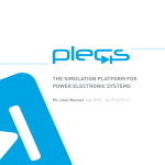
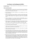
SEMIS – ABB semiconductor simulation tool Web manual - two-level VSC ABB Semiconductors introduces the new web based semiconductor simulation tool SEMIS. Providing thermal calculation of the semiconductor losses for common converter circuits, largely simplifies the selection of the device best fitting for your application. The SEMIS tool is a user friendly online application found on ABB Semiconductors website: www.abb.com/semiconductors SEMIS users can select the desired circuit parameters and HiPak IGBT modules. Based on the available range of options according to the parameters selected, multiple ABB HiPak modules can be simulated at the same time. Once a simulation is run, SEMIS returns results on semiconductor losses as well as on the electrical parameters in the input and output of the circuit. The results are shown in both graphical (waveforms) and numerical (tables) way. The SEMIS tool is based on the PLECS simulation software. PLECS users can download our product models in the XML file format from the ABB Semiconductors website and use them for their own simulations. ABB also supports on customised converter simulation with PLECS on a project basis. Contents 1. Two-level VSC3 1.1 Page layout 3 2. Inputs5 2.1 Circuit parameters 5 2.1.1 DC link voltage 5 2.1.2 Controller5 2.1.3 Ambient temperature 6 2.1.4 Load parameters 6 2.2 IGBT product selection 7 2.2.1 IGBT selection 7 2.2.2 IGBT module type selection 7 2.2.3 Matching IGBTs 7 2.3 Heatsink thermal resistance 7 3. Output results8 3.1 Graphical output – semiconductor waveforms 8 3.2 Graphical output – global scope waveforms 8 3.3 Results table 9 3.31 Definitions of input output results10 4. Alerts & features11 4.1 DC voltage alert 11 4.2 Temperature alert 11 2 SEMIS – ABB semicondcutor simulation tool | Web manual - two-level VSC 1.Two-level VSC 1.1 Page layout When the SEMIS tool web page is selected the following screen will appear. Fig.1 Page layout of two-level VSC in web host. 3 SEMIS – ABB semicondcutor simulation tool | Web manual - two-level VSC Each section of the user interface page is indicated in the next figure. 1 4 2 3 5 Secion-1 : Schematic circuit configuration used for the simulation Section-2: Selection of IGBT and circuit parameters Section-3: Simulation buttons Section-4: Graphical presentation of output and input waveforms Section-5 : Tabular presentation of circuit parameters. 4 SEMIS – ABB semicondcutor simulation tool | Web manual - two-level VSC 2. Inputs 2.1 Circuit parameters The circled elements shown in grey colour in the circuit schematic below can be clicked to enter corresponding values. 2.1.1 DC link voltage The user can select the desired DC link voltage from a range of 200 V≤V_dc≤4500 V. However, depending on the voltage class of the selected IGBT module, an overvoltage alarm message may pop up (see section 4.1). Please confirm value by clicking OK button ONLY. 2.1.2 Controller The user can define the following parameters as seen when clicking on the controller block: Please confirm values by clicking OK button ONLY. 5 SEMIS – ABB semicondcutor simulation tool | Web manual - two-level VSC • FREQUENCY (Converter AC output frequency) : selection range 10 to 100 Hz • SWITCHING FREQUENCY: selection range 200 to 5000 Hz • MODULATION INDEX: selection range 0 to1 • PWM STRATEGY: out of the following options: -> Symmetrical carrier -> Saw tooth carrier -> Symmetrical space-vector -> Alternating space vector 2.1.3 Ambient temperature The user can define the desired ambient temperature. The temperature ranges from -25 °C to 90 °C. Please confirm value by clicking OK button ONLY. 2.1.4 Load parameters By clicking the OUTPUT REFERENCE tab the user can select the desired parameter between Load Power and Load Current. Depending on the selection the user can get the below screens: Load Power: selection range 50 to 2000 kW Load Current: selection range up to 5000 A Power Factor: selection range 0.1 to 0.95 inductive 6 SEMIS – ABB semicondcutor simulation tool | Web manual - two-level VSC 2.2 IGBT product selection The user can select and test various IGBT types by entering the following parameters: 2.2.1 IGBT selection The user can select the desired IGBT voltage class from the available range. 2.2.2 IGBT module type selection The user can select the desired IGBT electrical configuration from the available options. 2.2.3 Matching IGBTs Once the previous IGBT properties are selected the matching HiPak IGBT options appear. By clicking on the part number the user can access the data sheet from the ABB website. The user can select the desired IGBT module for simulation. Up to 5 elements can be simulated simulatenously. If one or more elements produce results exceeding the safe operating area (SOA) then they will return no results. In this case the user should run the simulation again changing parameters and/or the product selection suitably, so that the results are within the SOA. 2.3 Heat sink thermal resistance The heat sink Rth value can be entered by the user through the input section. The value entered is attributed to each individual switch shown in the electrical configuration schematic of the IGBT module data sheet. Therefore if the user selects a dual switch module the Rth should be multiplied with a factor of 2 to differentiate from the single switch case. The same applies for the case of half bridge modules. 7 SEMIS – ABB semicondcutor simulation tool | Web manual - two-level VSC 3. Output results As soon as the user has defined all necessary parameters he may run the simulation by pressing the relevant button. The output results are displayed in two different ways: as graphical and tabular outputs. 3.1 Graphical output – semiconductor waveforms As soon as the simulation finishes the semiconductor waveforms appear as follows: The available buttons allow for the following: 1. Hide selectively waveforms of products. 2. Make all generated product waveforms available for the next simulation. 3. Selectively hold results for the next simulation. If one waveform is been selected to be kept for the next simulation then its symbol indication changes to red. If one clicks on the red symbol it is then deleted. 4. Cursor button reveals the 2 cursors on each graph and also a comprehensive table that also serves as legend for the waveforms. By moving the cursors horizontally user may determine the diference in value between 2 desired time instants. 5. Zoom buttons allow to zoom in by scrolling on the desired waveform and reset the initial view. 3.2 Graphical output – global scope waveforms If the user clicks on the Global Scope box in the circuit schematic. 8 SEMIS – ABB semicondcutor simulation tool | Web manual - two-level VSC Then additional output waveforms appear: Same features are available for these graphs as presented previously for the semiconductor graphs. The hide/hold buttons have the same effect for these graphs as well. 3.3 Results table The following parameters are given in a tabular format. 1. Input parameters 2. Output parameters 3. Device losses and temperatures Hold/Hide functions have the same influence on the results table as was previously described for the graphs. When simulating many devices at the same time, the results appear in relation to the selected product order as shown below: 9 SEMIS – ABB semicondcutor simulation tool | Web manual - two-level VSC 3.3.1 Definitions of input-output results Device losses & temperatures Switching losses: losses during turn on and turn off events (dynamic) based on ABB data sheet values. Conduction losses: losses during on state (static) based on ABB data sheet values. Combined losses = Switching losses + Conduction losses Input parameters: DC power: real power absorbed from the DC side of the VSC is calculated as: DC Power = DC Voltage x DC Current DC voltage: selected DC link voltage Modulation index: selected value from controller block Output parameters: Real power: power transferred to converter output is calculated as: Real Power = DC Power - Converter Losses (combined) According to: 10 SEMIS – ABB semicondcutor simulation tool | Web manual - two-level VSC It includes all harmonic components’ contribution, NOT ONLY the 1st order of the output frequency Phase Voltage (True RMS): AC line to neutral value according to: It includes all harmonic components, NOT ONLY the 1st order of the output frequency. Phase Current (True RMS): AC phase value according to: It includes all harmonic components, NOT ONLY the 1st order of the output frequency. PF: the user defined Load parameter corresponding to the desired angle between fundamental components of phase voltage and current Losses (%): defined as : 4. Alerts & features 4.1 DC voltage alert Each IGBT has a dc voltage limitation as per the table below. IGBT voltage rating DC link voltage range 1.7 kV 200 V to 1000V 2.5 kV 200 V to 1500V 3.3 kV 200 V to 2600V 4.5 kV 200 V to 3400V 6.5 kV 200 V to 4500V Alert features are added in the simulation if the above limits are violated. The alert message for each IGBT case is will appear as follows For 1.7 kV IGBT Vdcmin = 200 V & Vdcmax = 1300 V For 2.5 kV IGBT Vdcmin = 200 V & Vdcmax = 1500 V For 3.3 kV IGBT Vdcmin = 200 V & Vdcmax = 2600 V For 4.5 kV IGBT Vdcmin = 200 V & Vdcmax = 3400 V For 6.5 kV IGBT Vdcmin = 200 V & Vdcmax = 4500 V 4.2 Temperature alert When the junction temperature of the IGBT and diode is above its allowed value, an alert message will be displayed as follows IGBT temperature out of safe operating area! Diode temperature out of safe operating area! 11 SEMIS – ABB semicondcutor simulation tool | Web manual - two-level VSC ABB Switzerland Ltd. Semiconductors Fabrikstrasse 3 5600 Lenzburg, Switzerland Phone: +41 58 586 1419 Fax: +41 58 586 1306 E-Mail: [email protected] www.abb.com/semiconductors Note We reserve all rights in this document and in the subject matter and illustrations contained therein. Any reproduction, disclosure to third parties or utilization of its contents – in whole or in parts – is forbidden without prior written consent of ABB AG. Copyright© 2014 ABB All rights reserved SEMIS - Web manual - two-level VSC Contact us