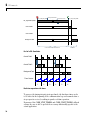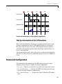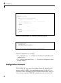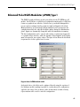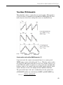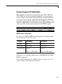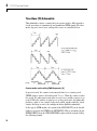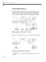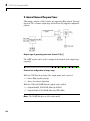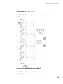
1
THE SIMULATION PLATFORM FOR
POWER ELECTRONIC SYSTEMS
PIL User Manual July 2015 - for PLECS 3.7
How to Contact Plexim:
%
+41 44 533 51 00
Phone
+41 44 533 51 01
Fax
)
Plexim GmbH
Technoparkstrasse 1
8005 Zurich
Switzerland
Mail
@
[email protected]
Email
http://www.plexim.com
Web
PIL User Manual
© 2015 by Plexim GmbH
The software PLECS described in this manual is furnished under a license
agreement. The software may be used or copied only under the terms of the
license agreement. No part of this manual may be photocopied or reproduced
in any form without prior written consent from Plexim GmbH.
PLECS is a registered trademark of Plexim GmbH. MATLAB, Simulink and
Simulink Coder are registered trademarks of The MathWorks, Inc. Other
product or brand names are trademarks or registered trademarks of their respective holders.
Contents
Contents
Before You Begin
iii
3
Installing the PIL Demo Projects . . . . . . . . . . . . . . . . . . . . . . .
3
What’s New in this Version . . . . . . . . . . . . . . . . . . . . . . . . . .
4
Major New Features . . . . . . . . . . . . . . . . . . . . . . . . . . .
4
Further Enhancements . . . . . . . . . . . . . . . . . . . . . . . . . .
4
1 Processor-in-the-Loop
5
Motivation . . . . . . . . . . . . . . . . . . . . . . . . . . . . . . . . . . . .
5
How PIL Works . . . . . . . . . . . . . . . . . . . . . . . . . . . . . . . . .
6
PIL Modes . . . . . . . . . . . . . . . . . . . . . . . . . . . . . . . . . . . .
8
Configuring PLECS for PIL . . . . . . . . . . . . . . . . . . . . . . . . . .
9
Target Manager . . . . . . . . . . . . . . . . . . . . . . . . . . . . . . . . .
9
Communication Links . . . . . . . . . . . . . . . . . . . . . . . . . .
10
PIL Block . . . . . . . . . . . . . . . . . . . . . . . . . . . . . . . . . . . . .
12
2 PIL Framework
17
Overview . . . . . . . . . . . . . . . . . . . . . . . . . . . . . . . . . . . . .
17
PIL Prep Tool . . . . . . . . . . . . . . . . . . . . . . . . . . . . . . . . . .
18
Probes . . . . . . . . . . . . . . . . . . . . . . . . . . . . . . . . . . . . . . .
18
Read Probes . . . . . . . . . . . . . . . . . . . . . . . . . . . . . . . .
18
Override Probes . . . . . . . . . . . . . . . . . . . . . . . . . . . . . .
20
Contents
Calibrations . . . . . . . . . . . . . . . . . . . . . . . . . . . . . . . . . . .
23
Code Identity . . . . . . . . . . . . . . . . . . . . . . . . . . . . . . . . . .
23
Remote Agent . . . . . . . . . . . . . . . . . . . . . . . . . . . . . . . . . .
24
Communication Callbacks . . . . . . . . . . . . . . . . . . . . . . . .
25
Serial Communication . . . . . . . . . . . . . . . . . . . . . . . . . .
25
Parallel Communication . . . . . . . . . . . . . . . . . . . . . . . . .
25
Framework Integration and Execution . . . . . . . . . . . . . . . . . . .
26
Principal Framework Calls . . . . . . . . . . . . . . . . . . . . . . .
26
Control Callback . . . . . . . . . . . . . . . . . . . . . . . . . . . . . .
30
Target Mode Switching . . . . . . . . . . . . . . . . . . . . . . . . . .
31
Simulation Start and Termination . . . . . . . . . . . . . . . . . . .
32
Control Dispatching . . . . . . . . . . . . . . . . . . . . . . . . . . . .
33
Task Synchronization at Start of Simulation . . . . . . . . . . . . .
35
Framework Configuration . . . . . . . . . . . . . . . . . . . . . . . . . . .
35
Configuration Constants . . . . . . . . . . . . . . . . . . . . . . . . . . . .
36
Initialization Constants . . . . . . . . . . . . . . . . . . . . . . . . . . . .
37
3 TI C2000 Peripheral Models
iv
39
Introduction . . . . . . . . . . . . . . . . . . . . . . . . . . . . . . . . . . .
39
Enhanced Pulse Width Modulator (ePWM) Type 1 . . . . . . . . . . . .
41
Supported Submodules and Functionalities . . . . . . . . . . . . . .
42
Time-Base (TB) Submodule . . . . . . . . . . . . . . . . . . . . . . .
43
Counter-Compare (CC) Submodule . . . . . . . . . . . . . . . . . . .
45
Action-Qualifier (AQ) Submodule . . . . . . . . . . . . . . . . . . . .
46
Event-Trigger (ET) Submodule . . . . . . . . . . . . . . . . . . . . .
50
Dead-Band Submodule . . . . . . . . . . . . . . . . . . . . . . . . . .
52
Enhanced Pulse Width Modulator (ePWM) Type 4 . . . . . . . . . . . .
54
Supported Submodules and Functionalities . . . . . . . . . . . . . .
55
Time-Base (TB) Submodule . . . . . . . . . . . . . . . . . . . . . . .
56
Counter-Compare (CC) Submodule . . . . . . . . . . . . . . . . . . .
58
Action-Qualifier (AQ) Submodule . . . . . . . . . . . . . . . . . . . .
59
Contents
Event-Trigger (ET) Submodule . . . . . . . . . . . . . . . . . . . . .
63
Dead-Band Submodule . . . . . . . . . . . . . . . . . . . . . . . . . .
66
Analog Digital Converter (ADC) Type 2 . . . . . . . . . . . . . . . . . . .
69
ADC Module Overview . . . . . . . . . . . . . . . . . . . . . . . . . .
70
ADC Converter with Result Registers . . . . . . . . . . . . . . . . .
71
ADC Sampling Mode . . . . . . . . . . . . . . . . . . . . . . . . . . .
72
ADC Sequencer Mode . . . . . . . . . . . . . . . . . . . . . . . . . . .
73
ADC Trigger and Interrupt Logic . . . . . . . . . . . . . . . . . . . .
75
Summary of PLECS Implementation . . . . . . . . . . . . . . . . .
76
Analog Digital Converter (ADC) Type 3 . . . . . . . . . . . . . . . . . . .
78
ADC Module Overview . . . . . . . . . . . . . . . . . . . . . . . . . .
79
ADC Converter with Result Registers . . . . . . . . . . . . . . . . .
80
ADC Reference Voltage Generator . . . . . . . . . . . . . . . . . . .
80
ADC Sample Generation Logic . . . . . . . . . . . . . . . . . . . . .
81
ADC Input Circuit . . . . . . . . . . . . . . . . . . . . . . . . . . . .
84
ADC Interrupt Logic . . . . . . . . . . . . . . . . . . . . . . . . . . .
85
Analog Digital Converter (ADC) Type 4 . . . . . . . . . . . . . . . . . . .
87
ADC Module Overview . . . . . . . . . . . . . . . . . . . . . . . . . .
89
ADC Converter and Result Register . . . . . . . . . . . . . . . . . .
89
ADC SOC Arbitration & Control . . . . . . . . . . . . . . . . . . . .
91
ADC Input Circuit . . . . . . . . . . . . . . . . . . . . . . . . . . . .
94
ADC Interrupt Logic . . . . . . . . . . . . . . . . . . . . . . . . . . .
95
Post-Processing Blocks . . . . . . . . . . . . . . . . . . . . . . . . . .
97
Enhanced Capture (eCAP) Type 0 . . . . . . . . . . . . . . . . . . . . . . 102
eCAP Module Operated in Capture Mode . . . . . . . . . . . . . . . 103
Event Prescaler . . . . . . . . . . . . . . . . . . . . . . . . . . . . . . 103
Edge Polarity Select and Capture Control . . . . . . . . . . . . . . . 104
eCAP Module Operated in APWM Mode
. . . . . . . . . . . . . . . 105
eCAP Interrupts . . . . . . . . . . . . . . . . . . . . . . . . . . . . . . 105
eCAP Counter Update . . . . . . . . . . . . . . . . . . . . . . . . . . 106
Summary of PLECS Implementation . . . . . . . . . . . . . . . . . 106
v
Contents
4 STM32 F4xx Peripheral Models
109
Introduction . . . . . . . . . . . . . . . . . . . . . . . . . . . . . . . . . . . 109
System Timer for PWM Generation (Output Mode) . . . . . . . . . . . . 111
Timer Subtypes . . . . . . . . . . . . . . . . . . . . . . . . . . . . . . 112
General Counter Behavior . . . . . . . . . . . . . . . . . . . . . . . . 112
Interrupt Flags . . . . . . . . . . . . . . . . . . . . . . . . . . . . . . 115
Output Mode Controller . . . . . . . . . . . . . . . . . . . . . . . . . 116
4 channel Advanced Timer . . . . . . . . . . . . . . . . . . . . . . . . 118
4 channel General Purpose Timer . . . . . . . . . . . . . . . . . . . 120
2 channel General Purpose Timer . . . . . . . . . . . . . . . . . . . 122
1 channel General Purpose Timer . . . . . . . . . . . . . . . . . . . 123
GPIO Mode . . . . . . . . . . . . . . . . . . . . . . . . . . . . . . . . . 125
Analog-Digital Converter (ADC) . . . . . . . . . . . . . . . . . . . . . . . 126
ADC Module Overview . . . . . . . . . . . . . . . . . . . . . . . . . . 127
ADC Converter with Result Registers . . . . . . . . . . . . . . . . . 128
ADC Sample Logic . . . . . . . . . . . . . . . . . . . . . . . . . . . . 129
ADC Interrupt Logic . . . . . . . . . . . . . . . . . . . . . . . . . . . 134
5 Microchip dsPIC33F Peripheral Models
137
Introduction . . . . . . . . . . . . . . . . . . . . . . . . . . . . . . . . . . . 137
Microchip Motor Control PWM . . . . . . . . . . . . . . . . . . . . . . . . 139
MCPWM Module Overview . . . . . . . . . . . . . . . . . . . . . . . 140
PWM Clock Control . . . . . . . . . . . . . . . . . . . . . . . . . . . . 141
PWM Output Control and Resolution . . . . . . . . . . . . . . . . . 143
Special Event Trigger . . . . . . . . . . . . . . . . . . . . . . . . . . . 144
Interrupt Control . . . . . . . . . . . . . . . . . . . . . . . . . . . . . 145
Dead Time Generator . . . . . . . . . . . . . . . . . . . . . . . . . . . 146
Summary of PLECS Implementation . . . . . . . . . . . . . . . . . 147
Microchip Motor Control ADC
. . . . . . . . . . . . . . . . . . . . . . . . 148
MCADC Module Overview . . . . . . . . . . . . . . . . . . . . . . . . 149
ADC Configuration . . . . . . . . . . . . . . . . . . . . . . . . . . . . 150
vi
Contents
ADC Sampling and Conversion . . . . . . . . . . . . . . . . . . . . . 152
Multi-channel ADC Sampling Mode . . . . . . . . . . . . . . . . . . 153
ADC Input Selection Mode . . . . . . . . . . . . . . . . . . . . . . . . 155
ADC Interrupt Logic . . . . . . . . . . . . . . . . . . . . . . . . . . . 157
ADC Buffer Fill Mode . . . . . . . . . . . . . . . . . . . . . . . . . . 158
Summary of PLECS Implementation . . . . . . . . . . . . . . . . . 158
6 Components by Category
161
Peripheral Blocks TI C2000 . . . . . . . . . . . . . . . . . . . . . . . . . . 161
Peripheral Blocks STM32 F4 . . . . . . . . . . . . . . . . . . . . . . . . . 162
Peripheral Blocks Microchip dsPIC33F . . . . . . . . . . . . . . . . . . . 162
7 Component Reference
165
TI C2000 ADC Type 2 GUI . . . . . . . . . . . . . . . . . . . . . . . . . . 166
TI C2000 ADC Type 2 REG . . . . . . . . . . . . . . . . . . . . . . . . . . 168
TI C2000 ADC Type 3 GUI . . . . . . . . . . . . . . . . . . . . . . . . . . 170
TI C2000 ADC Type 3 REG . . . . . . . . . . . . . . . . . . . . . . . . . . 172
TI C2000 ADC Type 3 Simplified . . . . . . . . . . . . . . . . . . . . . . . 174
TI C2000 ADC Type 4 GUI . . . . . . . . . . . . . . . . . . . . . . . . . . 176
TI C2000 ADC Type 4 REG . . . . . . . . . . . . . . . . . . . . . . . . . . 179
TI C2000 eCAP Type 0 APWM GUI . . . . . . . . . . . . . . . . . . . . . 182
TI C2000 eCAP Type 0 CAP GUI . . . . . . . . . . . . . . . . . . . . . . . 183
TI C2000 eCAP Type 0 CAP REG . . . . . . . . . . . . . . . . . . . . . . 185
TI C2000 ePWM Type 1 Configurator . . . . . . . . . . . . . . . . . . . . 186
TI C2000 ePWM Type 1 GUI . . . . . . . . . . . . . . . . . . . . . . . . . 188
TI C2000 ePWM Type 1 REG . . . . . . . . . . . . . . . . . . . . . . . . . 191
TI C2000 ePWM Type 4 Configurator . . . . . . . . . . . . . . . . . . . . 193
TI C2000 ePWM Type 4 GUI . . . . . . . . . . . . . . . . . . . . . . . . . 196
TI C2000 ePWM Type 4 REG . . . . . . . . . . . . . . . . . . . . . . . . . 200
STM32 F4 ADC GUI . . . . . . . . . . . . . . . . . . . . . . . . . . . . . . 203
STM32 F4 ADC REG . . . . . . . . . . . . . . . . . . . . . . . . . . . . . . 206
vii
Contents
STM32 F4 Timer Output Configurator . . . . . . . . . . . . . . . . . . . 208
STM32 F4 Timer Output GUI
. . . . . . . . . . . . . . . . . . . . . . . . 209
STM32 F4 Timer Output REG . . . . . . . . . . . . . . . . . . . . . . . . 212
MC dsPIC33F MCADC GUI . . . . . . . . . . . . . . . . . . . . . . . . . . 214
MC dsPIC33F MCADC REG . . . . . . . . . . . . . . . . . . . . . . . . . 217
MC dsPIC33F MCPWM GUI . . . . . . . . . . . . . . . . . . . . . . . . . 219
MC dsPIC33F MCPWMx GUI
. . . . . . . . . . . . . . . . . . . . . . . . 221
MC dsPIC33F MCPWM REG . . . . . . . . . . . . . . . . . . . . . . . . . 224
Processor-in-the-Loop . . . . . . . . . . . . . . . . . . . . . . . . . . . . . . 226
1
Contents
2
Before You Begin
Installing the PIL Demo Projects
The PLECS PIL package includes a number of demo projects to facilitate getting started with PIL. These demo projects implement typical power conversion applications such as motor drives and grid-tied inverters and are configured for different microprocessors.
Note A separate license is required to enable the PIL functionality in PLECS
and access the PIL demo projects.
To install the demo projects and associated documentation in a location of
your choice select PLECS Extensions. . . from the File menu. Then, on the
PIL tab, configure the desired destination folder (PIL Framework Path) and
install the packages of interest.
Note Make sure you install the Tools package as it contains the PIL Prep
Tool – see “PIL Prep Tool” (on page 18) – which is required by most demo
projects.
Included with the PIL demo projects are precompiled binaries as well as complete source code projects that can be imported into the appropriate IDE.
The source code of the PIL framework library can be obtained upon request.
Before You Begin
What’s New in this Version
Major New Features
• The new PIL Prep Tool simplifies the configuration of probes by parsing the
source code and automatically generating configuration files.
• New PIL Calibrations permit configuring embedded control algorithms directly from PLECS. Run multiple simulations and compare results with different settings for, e.g., filter coefficients and regulator gains, without recompiling the embedded code.
• Microchip dsPIC33F and STM 32F4 support added to PIL module, including
high-fidelity peripheral models.
Further Enhancements
• TI 2837x dual-core Delfino peripheral models added to PIL component library.
• Improved PIL communication protocol to support large probe count.
• Additional PIL callback to facilitate simulations of code using the TI Control Law Accelerator (CLA) coprocessor.
• Initial values for PIL override probes can now be set directly in PLECS.
4
1
Processor-in-the-Loop
As a separately licensed feature, PLECS offers support for Processor-in-theLoop (PIL) simulations, allowing the execution of control code on external
hardware tied into the virtual world of a PLECS model.
At the PLECS level, the PIL functionality consists of a specialized PIL block
that can be found in the Processor-in-the-loop library, as well as the Target
Manager, accessible from the Window menu. Also included with the PIL
library are high-fidelity peripheral models of MCUs used for the control of
power conversion systems.
On the embedded side, a PIL Framework library is provided to facilitate the
integration of PIL functionality into your project.
Motivation
When developing embedded control algorithms, it is quite common to be testing such code, or portions thereof, by executing it inside a circuit simulator.
Using PLECS, this can be easily achieved by means of a C-Script or DLL
block. This approach is referred to as Software-in-the-loop (SIL). A SIL simulation compiles the embedded source code for the native environment of the
simulation tool (e.g. Win64) and executes the algorithms within the simulation
environment.
The PIL approach, on the other hand, executes the control algorithms on the
real embedded hardware. Instead of reading the actual sensors of the power
converter, values calculated by the simulation tool are used as inputs to the
embedded algorithm. Similarly, outputs of the control algorithms executing
on the processor are fed back into the simulation to drive the virtual environment. Note that SIL and PIL testing are also relevant when the embedded
code is automatically generated from the simulation model.
1
Processor-in-the-Loop
One of the major advantages of PIL over SIL is that during PIL testing, actual compiled code is executed on the real MCU. This allows the detection of
platform-specific software defects such as overflow conditions and casting errors. Furthermore, while PIL testing does not execute the control algorithms
in true real-time, the control tasks do execute at the normal rate between two
simulation steps. Therefore, PIL simulation can be used to detect and analyze potential problems related to the multi-threaded execution of control algorithms, including jitter and resource corruption. PIL testing can also provide
useful metrics about processor utilization.
How PIL Works
At the most basic level, a PIL simulation can be summarized as follows:
Principle of a PIL simulation
• Input variables on the target, such as current and voltage measurements,
are overridden with values provided by the PLECS simulation.
• The control algorithms are executed for one control period.
• Output variables on the target, such as PWM peripheral register values,
are read and fed back into the simulation.
6
How PIL Works
We refer to variables on the target which are overridden by PLECS as Override Probes. Variables read by PLECS are called Read Probes.
While Override Probes are set and Read Probes are read the dispatching of
the embedded control algorithms must be stopped. The controls must remain
halted while PLECS is updating the simulated model. In other words, the control algorithm operates in a stepped mode during a PIL simulation. However,
as mentioned above, when the control algorithms are executing, their behavior
is identical to a true real-time operation. We therefore call this mode of operation pseudo real-time.
Let us further examine the pseudo real-time operation in the context of an
embedded application utilizing nested control loops where fast high-priority
tasks (such as current control) interrupt slower lower-priority tasks (such as
voltage control). An example of such a configuration with two control tasks is
illustrated in the figure below. With every hardware interrupt (bold vertical
bar), the lower priority task is interrupted and the main interrupt service routine is executed. In addition, the lower priority task is periodically triggered
using a software interrupt. Once both control tasks have completed, the system continues with the background task where lowest priority operations are
processed. The timing in this figure corresponds to true real-time operation.
Control Task 1
Control Task 2
Background Task
1
2
3
4
5
6
Nested Control Tasks
The next figure illustrates the timing of the same controller during a PIL simulation, with the stop and go symbols indicating when the dispatching of the
control tasks is halted and resumed.
After the hardware interrupt is received, the system stops the control dispatching and enters a communication loop where the values of the Override
Probes and Read Probes can be exchanged with the PLECS model. Once a
new step request is received from the simulation, the task dispatching is
7
1
Processor-in-the-Loop
STOP
STOP
STOP
Control Task 1
Control Task 2
Background Task
1
2
3
Pseudo real-time operation
restarted and the control tasks execute freely during the duration of one interrupt period. This pseudo real-time operation allows the user to analyze the
control system in a simulation environment in a fashion that is behaviorally
identical to a true real-time operation. Note that only the dispatching of the
control tasks is stopped. The target itself is never halted as communication
with PLECS must be maintained.
PIL Modes
The concept of using Override Probes and Read Probes allows tying actual
control code executing on a real MCU into a PLECS simulation without the
need to specifically recompile it for PIL.
You can think of Override Probes and Read Probes as the equivalent of test
points which can be left in the embedded software as long as desired. Software modules with such test points can be tied into a PIL simulation at any
time.
Often, Override Probes and Read Probes are configured to access the registers
of MCU peripherals, such as analog-to-digital converters (ADCs) and pulsewidth modulation (PWM) modules. Additionally, specific software modules, e.g.
a filter block, can be equipped with Override Probes and Read Probes. This
allows unit-testing the module in a PIL simulation isolated from the rest of
the embedded code.
To permit safe and controlled transitions between real-time execution of the
control code, driving an actual plant, and pseudo real-time execution, in con8
Configuring PLECS for PIL
junction with a simulated plant, the following two PIL modes are distinguished:
• Normal Operation – Regular target operation in which PIL simulations
are inhibited.
• Ready for PIL – Target is ready for a PIL simulation, which corresponds
to a safe state with the power-stage disabled.
The transition between the two modes can either be controlled by the embedded application, for example based on a set of digital inputs, or from PLECS
using the Target Manager.
Configuring PLECS for PIL
Once an embedded application is equipped with the PIL framework, and appropriate Override Probes and Read Probes are defined, it is ready for PIL
simulations with PLECS.
PLECS uses the concept of Target Configurations to define global high-level
settings that can be accessed by any PLECS model. At the circuit level, the
PIL block is utilized to define lower level configurations such as the selection
of Override Probes and Read Probes used during simulation.
This is explained in further detail in the following sections.
Target Manager
The high-level configurations are made in the Target Manager, which is accessible in PLECS by means of the corresponding item in the Window menu.
The target manager allows defining and configuring targets for PIL simulation, by associating them with a symbol file and specifying the communication
parameters. Target configurations are stored globally at the PLECS level and
are not saved in *.plecs or Simulink files. An example target configuration is
shown in the figure below.
9
1
Processor-in-the-Loop
Target Manager
The left hand side of the dialog window shows a list of targets that are currently configured. To add a new target configuration, click the button marked
+ below the list. To remove the currently selected target, click the button
marked -. You can reorder the targets by clicking and dragging an entry up
and down in the list.
The right hand side of the dialog window shows the parameter settings of
the currently selected target. Each target configuration must have a unique
Name.
The target configuration specifies the Symbol file and the communication
link settings.
The symbol file is the binary file (also called “object file”) corresponding to the
code executing on the target. PLECS will obtain most settings for PIL simulations, as well as the list of Override Probes and Read Probes and their attributes, from the symbol file.
Communication Links
A number of links are supported for communicating with the target. The desired link can be selected in the Device type combo box. For communication
links that allow detecting connected devices, pressing the Scan button will
populate the Device name combo box with the names of all available devices.
10
Target Manager
Serial Device
The Serial device selection corresponds to conventional physical or virtual
serial communication ports. On a Windows machine, such ports are labeled
COMn, where n is the number of the port.
FTDI Device
If the serial adapter is based on an FTDI chip, the low-level FTDI driver can
be used directly by selecting the FTD2XX option. This device type offers improved communication speed over the virtual communication port (VCP) associated with the FTDI adapter.
TCP/IP Socket
The communication can also be routed over a TCP/IP socket by selecting the
TCP Socket device type.
TCP/IP Communication
In this case the Device name corresponds to the IP address (or URL) and
port number, separated by a colon (:).
11
1
Processor-in-the-Loop
TCP/IP Bridge
The TCP Bridge device type provides a generic interface for utilizing custom
communication links. This option permits communication over an external application which serves as a “bridge” between a serial TCP/IP socket and a custom link/protocol.
Target Properties
By pressing the Properties button, target information can be displayed as
shown in the figure below.
Target Properties
In addition to reading and displaying information from the symbol file, PLECS
will also query the target for its identity and check the value against the one
stored in the symbol file. This verifies the device settings and ensures that the
correct binary file has been selected. Further, the user can request for a target
mode change to configure the embedded code to run in Normal Operation
mode or in Ready for PIL mode.
PIL Block
The PIL block ties a processor into a PLECS simulation by making Override
Probes and Read Probes, configured on the target, available as input and output ports, respectively.
12
PIL Block
PIL Block
A PIL block is associated with a target defined in the target manager, which
is selected from the Target combo box. The Configure. . . button provides a
convenient shortcut to the target manager for configuring existing and new
targets.
PIL Block General Tab
The execution of the PIL block can be triggered at a fixed Discrete-Periodic
rate by configuring the Sample time to a positive value. As with other
PLECS components, an Inherited sample time can be selected by setting the
parameter to -1 or [-1 0].
A trigger port can be enabled using the External trigger combo box. This is
useful if the control interrupt source is part of the PLECS circuit, such as an
ADC or PWM peripheral model.
13
1
Processor-in-the-Loop
Typically, an Inherited sample time is used in combination with a trigger
port. If a Discrete-Periodic rate is specified, the trigger port will be sampled
at the specified rate.
Similar to the DLL block, the Output delay setting permits delaying the output of each simulation step to approximate processor calculation time.
Note Make sure the value for the Output delay does not exceed the sample
time of the block, or the outputs will never be updated.
A delay of 0 is a valid setting, but it will create direct-feedthrough between
inputs and outputs.
PIL Block Inputs Tab
The PIL block extracts the names of Override Probes and Read Probes from
the symbol file selected in the target configuration and presents lists for selection as input and output signals, as shown in the figure above.
The number of inputs and outputs of a PIL block is configurable with the
Number of inputs and Number of outputs settings. To associate Over14
PIL Block
ride Probes or Read Probes with a given input or output, select an input/output from the combo box on the right half of the dialog. Then drag the desired
Override Probes or Read Probes from the left into the area below or add them
by selecting them and clicking the > button. To remove an Override Probe or
Read Probe, select it and either press the Delete key or < button.
Note It is possible to multiplex several Override/Read Probe signals into one
input/output. The sequence can be reordered by dragging the signals up and
down the list.
Starting with PLECS 3.7, the PIL block allows setting initial conditions for
Override Probes.
Also new with PLECS 3.7 is the Calibrations tab, which permits modifying
embedded code settings such as regulator gains and filter coefficients.
PIL Block Calibrations Tab
Calibrations can be set in the Value column. If no entry is provided, the embedded code will use the default value as indicated in the Default column.
15
1
16
Processor-in-the-Loop
2
PIL Framework
Plexim provides and maintains PIL Frameworks for specific processor families,
which encapsulate all the necessary embedded functionality for PIL operation.
Using the PIL framework, your C or C++ based embedded applications can be
enabled for PIL with minimal effort.
Currently, such frameworks and associated demo applications are available
for the Texas Instruments (TI) C2000™, ST Microelectronics 32bit F4 and the
Microchip dsPIC33F MCU families. However, support for other platforms can
be developed, as long as the following basic requirements are met:
• The code generation tools (compiler and linker) must be able to generate
binary files of the ELF format containing DWARF debugging information.
• The address width of the processor cannot exceed 32 bit.
• The least addressable unit (LAU) of the processor must be no larger than
16-bit.
Overview
The fundamental operation of a PIL simulation consists of overriding and
reading variables in the embedded application, and synchronizing the execution of the control task(s) with the simulation of a PLECS model. The PIL
framework therefore provides the following functionality:
• Read Probes for reading the values of variables in the embedded code executing on the target and feeding the information into the simulation model.
• Override Probes for overriding variables in the embedded code with values
obtained from the simulation.
• A method to uniquely identify the software executing on the target.
• A remote agent, capable of communicating with PLECS and interpreting
commands related to PIL operation.
2
PIL Framework
• A mechanism for stopping and starting the execution of the control tasks.
• A means to provide configuration parameters to PLECS, such as the communication baudrate.
Starting with PLECS 3.7, the PIL framework also supports Calibrations,
which are embedded–code parameters such as filter coefficients and regulator gains. Calibrations can be modified in the PLECS environment during the
initialization of a PIL simulation and allow running multiple simulations with
different settings without the need for recompiling the embedded code (e.g. for
the tuning of regulators).
PIL Prep Tool
To facilitate defining and configuring PIL probes and calibrations, starting
with PLECS 3.7, a PIL Prep Tool utility is provided as part of the PIL framework.
The PIL Prep Tool parses the embedded code for PIL specific macros, and automatically generates auxiliary files to be compiled and linked with the embedded code. These auxiliary files contain functions for initializing probes and
calibrations, as well as special symbols which describe to PLECS the scaling
and formatting of the probes/calibrations. The generated files further include
a globally unique identifier (GUID) allowing PLECS to identify the embedded
code.
The PIL Prep Tool must be called as a pre-build step. Its integration into an
embedded project is specific to the compiler and integrated development environment (IDE) used. Please refer to the PIL demo projects for more information.
Probes
Read Probes
Read Probes are variables in the embedded code which are configured for read
access by PLECS. Any global variable can be configured as a Read Probe by
means of the PIL_READ_PROBE macro. For example, the statement below defines and configures variable Vdc for read access by PLECS.
PIL_READ_PROBE(uint16_t , Vdc, 10, 5.0, "V");
18
Probes
The PIL_READ_PROBE macro results in a simple variable definition, e.g.
uint16_t Vdc, but is also recognized by the PIL Prep Tool, which places the
following statement in the auto generated file:
PIL_SYMBOL_DEF(Vdc, 10, 5.0, "V");
The PIL_SYMBOL_DEF macro expands into the definition of a specially formatted and statically initialized helper structure of type const.
typedef struct
{
int q;
float ref;
char *unit;
} pil_var;
//!< fixed−point location
//!< reference value
//!< unit string
const pil_var PIL_V_Vdc = {10, 5.0, "V"}
PLECS searches for PIL_V symbols when parsing the binary file selected in
the target manager, and uses the information of the PIL_V symbols to translate between the raw values stored in the Read Probe and the corresponding
physical value to be used in the simulation.
In the above example, the global variable Vdc is configured as a Q10 with a
reference of 5V. Hence, an integer value of 512 in this variable will be converted by PLECS to 512
210 ∗ 5V = 2.5V.
A fixed point variable can be configured as a unitless number by using a reference value of 1.0 and setting an empty string (“”) for the unit.
The same approach can be used to configure floating point variables as Read
Probes.
PIL_READ_PROBE(float, MotorSpeed, 0, 1.0, "rpm");
The third parameter of the PIL_READ_PROBE macro, i.e. the fixed point location, is ignored with probed floating point variables. However, it is possible to
specify reference values for floating point variables. For example, the macro
below configures MotorSpeed with a reference of 1800 rpm. Hence, a value of
0.5 in this variable will be converted to 0.5 ∗ 1800rpm = 900rpm.
It is also possible to configure structure members, as shown below.
19
2
PIL Framework
struct BATTERY {
PIL_READ_PROBE(int16_t, voltage, 10, 5.0, "V");
};
Override Probes
Override Probes, i.e. variables in the embedded code that can be overridden by
PLECS, are defined with the PIL_OVERRIDE_PROBE macro as illustrated below.
struct BATTERY {
PIL_OVERRIDE_PROBE(int16_t, voltage, 10, 5.0, "V");
};
struct BATTERY MyBattery;
The PIL_OVERRIDE_PROBE macro expands into a variable definition that is augmented by two helper symbols which permit the MyBattery.voltage variable
to be overridden by PLECS.
struct BATTERY {
int16_t voltage;
int16_t voltage_probeV;
int16_t voltage_probeF;
};
While parsing a binary file for symbol information, PLECS detects variables
with matching _probeF and _probeV definitions and identifies those as Override Probes.
In addition, the PIL Prep Tool will recognize the PIL_OVERRIDE_PROBE macro
and generate the following auxiliary macro as described in the Read Probe
section:
PIL_SYMBOL_DEF(MyBattery_voltage, 10, 5.0, "V");
Note Only variables defined as Override Probes are configurable as inputs for
the PIL block.
20
Probes
An Override Probe is similar to a toggle switch with the following two states:
• Feedthrough – The Override Probe value is provided by the embedded application
• Override – The Override Probe value is provided by PLECS
The state of an Override Probe can be switched dynamically at runtime and is
stored in the _probeF helper variable.
With this approach, the same build of the embedded application can be used
to control actual hardware or be tested in a PIL simulation, by simply switching the mode of Override Probes, without recompiling.
To properly interact with PLECS, the embedded code must access the Override Probes exclusively by the following set of macros:
Override Probe Macros
Macro
Description
INIT_OPROBE(probe)
Initializes an Override Probe.
Must be called during the initialization of the embedded
program.
SET_OPROBE(probe, value)
Assigns a value to an Override
Probe.
The PIL Prep Tool will generate a function called PilInitOverrideProbes()
which contains INIT_OPROBE calls for all Override Probes. This function must
be called during the initialization phase of the embedded code before any
Override Probes are used.
If an Override Probe is in the feedthrough state, the value assigned to the
macro is written into probe. Otherwise, the override value supplied by
PLECS is used, which is stored in the _probeV helper variable.
An example for adding Override Probes to existing code is given in the following two listings.
21
2
PIL Framework
Battery.voltage = measureBattVolt();
PLX_VECT_parkRot(ControlVars.Ia, ControlVars.Ib, \
&ControlVars.Id, &ControlVars.Iq, \
ControlVars.fluxPosSin, ControlVars.fluxPosCos);
Original code without use of Override Probes
Assume that during PIL simulations, we would like to override the variable Battery.voltage as well as the values of ControlVars.Id and
ControlVars.Iq. While the battery voltage is updated by a simple write access, the Id and Iq variables are modified by the PLX_VECT_parkRot(...) function via pointers, which need special handling for the SET_OPROBE macro integration.
The next listing illustrates how SET_OPROBE is properly used in this example.
SET_OPROBE(Battery.voltage, measureBattVolt());
int16_t id, iq;
PLX_VECT_parkRot(ControlVars.Ia, ControlVars.Ib, \
&id, &iq, \
ControlVars.fluxPosSin, ControlVars.fluxPosCos);
SET_OPROBE(ControlVars.Id, id);
SET_OPROBE(ControlVars.Iq, iq);
Use of Override Probes
For the battery voltage, the assignment can simply be replaced by the
SET_OPROBE macro. For the Id and Iq values, auxiliary variables are used,
updated by the PLX_VECT_parkRot(...) function, and subsequently assigned
to the Override Probes.
Note The SET_OPROBE macro must be used whenever a value is assigned to an
Override Probe. A direct assignment using the equal (=) statement will result in
unpredictable behavior.
22
Calibrations
Calibrations
Calibrations are variables used to configure algorithms in the embedded code,
such as filter coefficients, thresholds, timeouts and regulator gains.
The PIL framework provides the PIL_CALIBRATION macro for a convenient definition of such calibrations. For example, the statement below declares and
configures variable Kp as a PIL calibration.
PIL_CALIBRATION(int16_t, Kp, 10, 5.0, "Ohm", 0, 10.0, 0.5);
The first five parameters of the PIL_CALIBRATION macro are identical to the
definition of a Read Probe. Accordingly, the macro expands into a simple variable definition uint16_t Kp.
The additional three parameters define the allowable range of values for the
Calibration as well as its default value.
In the above example, the allowable range for Kp is 0 – 10Ω. Upon initialization, Kp is set to 0.5Ω.
The PIL_CALIBRATION macro is interpreted by the PIL Prep Tool to generate a PIL_SYMBOL_CAL_DEF macro. Similar to PIL_SYMBOL_DEF, this macro
produces the necessary information for PLECS to properly interpret and
handle the calibration. The PIL Prep Tool also generates a function called
PilInitCalibrations() which sets all Calibrations to default values. This
function must be called during the initialization phase of the embedded code
before any calibrations are used. It is also important that this function be
called in the PIL_CLBK_TERMINATE_SIMULATION callback to revert changes
made during a PIL simulation.
Code Identity
PLECS accesses Override Probes, Read Probes and Calibrations by address
(as opposed to name). The PIL block extracts the address of a given variable
from the debugging information contained in the binary file supplied to the
Target Manager. It is therefore important to ensure the selected binary file
matches the code that is actually executing on the target, or erroneous memory locations will be accessed. This is achieved by comparing a globally unique
23
2
PIL Framework
identifier (GUID) stored in the binary file with the value reported by the target. PLECS performs this check at the beginning of a simulation, as well as
when the PIL block is opened. As explained in section “Target Manager” (on
page 9), the target manager can be used to verify the match of the selected
binary file.
The GUID is generated at compile time by the PIL Prep Tool. Additionally,
macros for the compile time, and log-on name of the person who compiled the
code are created.
#define CODE_GUID {0xA8,0x45,0x11,0xDE,0x05,0x4C,0xAC,0x41}
#define COMPILE_TIME_DATE_STR "Sun May 30 10:11:43 2010"
#define USER_NAME "john doe"
The value of CODE_GUID is passed to the PIL framework during initialization;
see “Framework Configuration” (on page 35). The value must also be assigned
to the PIL_D_Guid constant as follows:
PIL_CONST_DEF(unsigned char, Guid[], CODE_GUID);
The other two macros can be used for diagnostics purposes using PIL constants, as demonstrated in section “Configuration Constants” (on page 36).
Remote Agent
The remote agent services the communication link with PLECS and processes
commands received from PLECS to access Override Probes and Read Probes,
and to step the control code during a PIL simulation.
The remote agent supports both parallel and serial communications, but is
agnostic of the hardware specific details of the communication link.
The user of the PIL framework is responsible for implementing the driver for
a specific communication link, i.e. for configuration of hardware and basic reception and transmission of data.
24
Remote Agent
Communication Callbacks
The PIL framework interacts with the application specific communication
driver by communication callback functions. Two callbacks exist:
• CommCallback() – Called at each system interrupt from
PIL_beginInterruptCall().
• BackgroundCommCallback() – Periodically called from
PIL_backgroundCall().
A given communication link might use either or both callbacks for its implementation. For implementing serial or parallel data exchange with the framework, the user needs to utilize the input and output functions presented in the
following sections. The callback functions are registered with the framework
as described on page 35.
Serial Communication
For serial communication, the remote agent utilizes a simple network layer
with message framing and error checking, making the protocol suitable for a
wide range of links such as RS-232, RS-485, TCP/IP and CAN.
To ensure no characters are dropped during a serial communication, the CommCallback() from the interrupt should be used to service the link.
A typical implementation of a serial communication callback is shown in the
SCI callback listing.
Notice the use of the following two functions:
• PIL_RA_serialIn(...) – For the reception of characters.
• PIL_RA_serialOut(...) – For the transmission of characters.
Parallel Communication
For parallel communication, complete messages are directly exchanged with
the framework as 16-bit integer arrays. The parallel link does not utilize any
framing or checksum. This link is therefore suited for exchanging messages
via shared memory where risk of transmission errors is negligible.
Parallel communications are typically serviced by the callback made from the
background loop.
• PIL_RA_parallelIn(...) – For the reception of a message.
• PIL_RA_parallelOut(...) – For the transmission of a message.
25
2
PIL Framework
void SCIPoll()
{
while(SciaRegs.SCIFFRX.bit.RXFFST != 0)
{
// a character has been received
PIL_RA_serialIn((int16)SciaRegs.SCIRXBUF.all);
}
int16_t ch;
if(SciaRegs.SCICTL2.bit.TXRDY == 1)
{
// link is ready for transmission
if(PIL_RA_serialOut(&ch))
{
SciaRegs.SCITXBUF = ch;
}
}
}
SCI callback
Framework Integration and Execution
Principal Framework Calls
The PIL framework provides the following two principal functions which must
be called periodically by the embedded application to enable PIL functionality:
• PIL_beginInterruptCall() – Framework call from interrupt.
• PIL_backgroundCall(...) – Framework call from background loop.
The PIL_beginInterruptCall() must be added at the beginning of the main
interrupt service routine, while the PIL_backgroundCall(...) is called periodically from the background task.
The actions performed by those calls depends on whether a PIL simulation is
running or not.
In the following, the concept of the PIL integration is further explained for a
system with nested control tasks (see code snippet below).
In this example, the first control task is triggered by a hardware interrupt related to the system counter. A divider is used to dispatch a second, lower priority task. When the divider reaches a specified value, the second control task
is dispatched by a software interrupt.
26
Framework Integration and Execution
/**
* Main interrupt routine
*/
Void TickFxn(UArg arg)
{
PIL_beginInterruptCall();
// fast control task
ControlTask1();
// slow control task
divider++;
if(divider == TASK2_PERIOD)
{
divider = 0;
Swi_post(Swi);
}
}
/**
* Software interrupt for slow control task
*/
Void SwiFxn(UArg arg0, UArg arg1)
{
ControlTask2();
}
/**
* Background task
*/
Void BackgroundTaskFxn(Void)
{
PIL_backgroundCall();
}
Control Task Dispatching
27
2
PIL Framework
Real-time
Pseudo Real-time
PIL_beginInterruptCall
CommCallback
CommCallback
BackgroundCommClbk
Message Evaluation
PIL Cmd Handling
PIL_backgroundCall
BackgroundCommClbk
Message Evaluation
PIL Cmd Handling
N/A
Mode-specific actions during framework execution
Assuming the slow task takes longer than a hardware interrupt period, the
second control task is interrupted several times before its execution is finished.
Now let us examine the operation of the framework in both real-time and
pseudo real-time mode.
The figure on page 28 shows the framework operation in non-PIL (real-time)
mode.
CommCallback
PIL_beginInterruptCall
Control Task 1
Control Task 2
Background Task
PIL_backgroundCall
PIL framework during real-time operation
At the beginning of the hardware interrupt service routine, the
PIL_beginInterruptCall() is executed, which, in real-time mode, only calls
28
Framework Integration and Execution
the registered CommCallback function. As already mentioned, this callback
should be used to service the link for a serial communication to ensure no
characters are dropped.
Note During real-time operation, the PIL framework must have a minimal
influence on the timing of the dispatched control tasks. Therefore the CommCallback function must be implemented as efficiently as possible.
As its name suggests, PIL_backgroundCall(...) function is executed from the
background loop, which in turn calls the BackgroundCommCallback(), if configured. The PIL_backgroundCall(...) also parses incoming messages that
are buffered by the communication callback functions, and processes PIL commands.
STOP
PILCLBK_STOP_TIMERS
CLBK_START_TIMERS
PIL_beginInterruptCall
PLECS Step
Control Task 1
Control Task 2
Background Task
Communication loop
PIL framework during pseudo real-time operation
The next figure shows the system behavior during a PIL simulation, i.e. in
pseudo real-time mode, where control task execution is paced and synchronized with the simulation of a PLECS model.
At the start of the hardware interrupt service routine, the task dispatching
stops and the system enters a communication loop.
29
2
PIL Framework
In this loop, both communication callbacks and the command parsing functions are executed. This is different from true real-time mode, where the background communication callback and the command parsing functions are called
from the background loop.
Once a request for a new control step is received, the framework resumes
the control task dispatching and continues in free mode until the next
hardware interrupt occurs. Note that in pseudo real-time operation, the
PIL_backgroundCall() has no effect.
Control Callback
The transition between different operating modes as well as the pseudo realtime operation require application-specific actions, implemented by means of a
Control Callback.
For example, when entering the Ready for PIL mode, the power actuation must be turned off, e.g. by disabling the PWM outputs. Also, during
a PIL simulation the peripherals providing the timing to the control algorithms must be stopped and restarted, as indicated by the arrows labeled
PIL_CLBK_STOP_TIMERS and PIL_CLBK_START_TIMERS.
These control actions are provided by a single callback function registered during the framework initialization, and subsequently executed with an argument
specifying the specific action to be taken.
Consequently, the implementation of this callback typically consists of a
switch statement as shown below:
The following control-callback actions are defined and called during the framework execution:
• PIL_CLBK_ENTER_NORMAL_OPERATION_REQ – Called when the target mode
“Normal Operation” has been requested. The application must indicate that
it has entered normal operation by executing PIL_inhibitPilSimulation().
• PIL_CLBK_LEAVE_NORMAL_OPERATION_REQ – Called when the target mode
“Ready for PIL” has been requested. The application must confirm that it
is ready for PIL simulations by executing PIL_allowPilSimulation().
• PIL_CLBK_PREINIT_SIMULATION – Called before transitioning to a PIL simulation. Can be used to reconfigure task dispatching, for example if an MCU
coprocessor such as the TI CLA is to be tied into the PIL loop. Interrupts
are disabled when this call is made.
30
Framework Integration and Execution
void PilCallback(PIL_CtrlCallbackReq_t aCallbackReq)
{
switch(aCallbackReq)
{
case PIL_CLBK_STOP_TIMERS:
//application specific code
break;
case PIL_CLBK_START_TIMERS:
//application specific code
break;
.
.
.
default:
//catching an undefined callback
break;
}
}
• PIL_CLBK_INITIALIZE_SIMULATION – Called at the beginning of a PIL simulation. Used to reset the controller(s) and control task dispatching to initial
conditions.
• PIL_CLBK_TERMINATE_SIMULATION – Called at the end of a PIL simulation.
• PIL_CLBK_STOP_TIMERS – Called at the beginning of the control interrupt
when in PIL mode (pseudo real-time operation). Used to stop all timers and
counters related to the control tasks.
• PIL_CLBK_START_TIMERS – Called immediately before resuming the control
task(s) when in PIL mode (pseudo real-time operation). Used to restart all
timers and counters related to the control tasks.
In the following sections, the different actions are further described in context
of when they are called during the operation of the PIL framework. Please
also review the example projects provided by Plexim for further details and
control callback implementation examples.
Target Mode Switching
As described in the section “PIL Modes” (on page 8) the PIL framework distinguishes between the two target modes.
In Normal Operation mode, the target executes in true real-time operation
driving the load with an active power stage. PIL simulations are inhibited
31
2
PIL Framework
Normal Operation
PIL_requestReadyMode
-> PIL_CLBK_LEAVE_NORMAL_OPERATION_REQ
do/Realtime Application
PIL_allowPilSimulation()
PIL_inhibitPilSimulation()
Ready for PIL
do/wait for start of PIL Simulation
PIL_requestNormalMode
-> PIL_CLBK_ENTER_NORMAL_OPERATION_REQ
PIL target modes and mode change requests
in this mode due to the power stage being active. A PIL simulation can only
be started if the target is in Ready for PIL mode, which corresponds to a safe
state in which the power stage is disabled. As explained in the prior section,
the code for enabling or disabling the power stage is application specific and
must be provided by the user via the corresponding control callback.
A target mode change can be requested either from the Target Manager or
from the embedded application. Depending on the requested mode, the framework executes the appropriate callback. If the requested mode is equal to the
current mode or while a PIL simulation is active, a mode request has no effect.
Target mode change requests are confirmed by the application code by calling
the PIL_allowPilSimulation() and PIL_inhibitPilSimualtion() functions.
Those functions also have no effect while a PIL simulation is active. Please
refer to the example projects provided by Plexim for further details and implementation examples.
Simulation Start and Termination
When running multiple PIL simulations and comparing results it is important that all simulation-runs begin with identical initial conditions. This is
32
Framework Integration and Execution
achieved by means of the PIL_CLBK_INITIALIZE_SIMULATION request, which is
issued via the control callback at the beginning of a simulation.
STOP
PIL_CLBK_STOP_TIMERS
Sending Initial Read Probe values
PIL_beginInterruptCall
PIL_CLBK_INITIALIZE_SIMULATION
Wait for 1. PIL Block Evaluation
Control Task 1
Control Task 2
Background Task
Start of PIL Simulation
Ready Mode
First Communication loop in Pseudo Real-time
Start of a PIL Simulation
Note The initial conditions of Read Probes are fed into the PLECS model at
simulation time t=0. However, these values will be immediately modified if the
PIL block is also triggered at time t=0 and the output delay of the block is set to
zero.
At the end of a PIL simulation, a PIL_CLBK_TERMINATE_SIMULATION request is
issued prior to returning to real-time operation.
Control Dispatching
During a PIL simulation, the target operates in a pseudo real-time fashion
with the execution of the control tasks being paced and synchronized with the
simulation.
In the example shown in the next figure, the interrupt for Control Task 1 is
based on the period of a hardware timer. Therefore, the timer period directly
determines the amount of time available for the execution of the control tasks
until the next interrupt occurs.
33
2
PIL Framework
STOP
PIL_CLBK_STOP_TIMERS
Sending Final Read Probes
PIL Simulation Finished
PIL_CLBK_START_TIMERS
PIL_beginInterruptCall
PIL_CLBK_TERMINATE_SIM
Control Task 1
Control Task 2
Background Task
Last Communication loop in Pseudo Real-time
Ready Mode
End of a PIL Simulation
Control Task 1
Control Task 2
Background Task
Timer Counter
1
2
3
4
5
6
Real-time operation with timer
To preserve the timing integrity in stepped mode, the hardware timer needs
to be halted at the beginning of the communication loop and resumed when a
step request is received, resulting in pseudo real-time operation.
By means of the CLBK_STOP_TIMERS and CLBK_START_TIMERS callback
actions, the user is able to provide the necessary functionality specific to the
actual application.
34
Framework Configuration
STOP
STOP
STOP
Control Task 1
Control Task 2
Background Task
Timer Counter
1
2
3
Pseudo real-time operation with periodically stopped timer
Task Synchronization at Start of Simulation
When control algorithms are distributed over multiple (nested) tasks, it is important to synchronize the start of a PIL simulation with the sequencing of
the control tasks. In other words, after a PIL simulation has been started, a
predictable and repeatable amount of time should elapse until the first execution of each nested task.
Such synchronization can be achieved by actively resetting the task dispatcher
when the PIL_CLBK_INITIALIZE_SIMULATION request is received, as illustrated
below.
Framework Configuration
The initialization and configuration of the PIL framework consists of three
mandatory steps as well as a number of optional configurations.
• PIL_init() – Must be executed before any calls to the framework are made.
• PIL_setLinkParams(...) – Specifies the GUID to the framework and registers the interrupt callback for communication.
• PIL_setCtrlCallback(...) – Registers the control callback for PIL simulations.
35
2
PIL Framework
void PilCallback(PIL_CtrlCallbackReq_t aCallbackReq)
{
switch(aCallbackReq)
{
case PIL_CLBK_INITIALIZE_SIMULATION:
//application specific code
...
//active synchronization of control task dispatching
divider = TASK2PERIOD −1;
break;
.
.
.
default:
//catching an undefined callback
break;
}
}
Active task synchronization via simulation initialization callback
PIL_init();
PIL_setLinkParams(\
(unsigned char*)&PIL_D_Guid[0], \
(PIL_CommCallbackPtr_t)SCIPoll
);
PIL_setCtrlCallback((PIL_CtrlCallbackPtr_t)PilCallback);
Optional configurations are as follows:
• PIL_setNodeAddress(...) – Configures node address for multi-drop serial
communications.
• PIL_setBackgroundCommCallback(...) – Registers the background communication callback.
Configuration Constants
The PIL_CONST_DEF macro is used for making settings and diagnostics information available to PLECS. At a minimum, Guid[] must be defined. If a serial link is used for communication between PLECS and the target, then it is
also necessary to specify to PLECS the communication rate by means of the
36
Initialization Constants
BaudRate definition. Optionally, further constants can be defined as shown be-
low.
PIL_CONST_DEF(unsigned char, Guid[], CODE_GUID);
PIL_CONST_DEF(unsigned char, CompiledDate[], COMPILE_TIME_DATE_STR);
PIL_CONST_DEF(unsigned char, CompiledBy[], USER_NAME);
PIL_CONST_DEF(uint32_t, BaudRate, BAUD_RATE);
PIL_CONST_DEF(uint16_t, StationAddress, 0);
PIL_CONST_DEF(char, FirmwareDescription[], "Demo project");
Note Depending on the build settings it might be necessary to provide specific
compiler/linker instructions (e.g. #pragma RETAIN) to prevent PIL definitions
and constants that are not referenced by the code from being removed from the
binary file.
Initialization Constants
The PIL framework also provides a mechanism to define “Initialization Constants” (or “Configurations”) that can be read from the symbol file at the beginning of a simulation and used to configure the PLECS circuit.
PIL_CONFIG_DEF macro is used for defining such constants. They must be of
integer or float type. Strings and arrays are not supported.
PIL_CONFIG_DEF(uint32_t,
PIL_CONFIG_DEF(uint32_t,
PIL_CONFIG_DEF(uint32_t,
PIL_CONFIG_DEF(uint16_t,
SysClk, SYSCLK_HZ);
PwmFrequency, PWM_HZ);
ControlFrequency, CONTROL_HZ);
ProcessorPartNumber, 28069);
To retrieve the values of the initialization constants in PLECS use the
plecs(’get’, ’path to PIL block’, ’InitConstants’) command either in a
m-file or in the model initialization commands.
37
2
PIL Framework
initConstants = plecs('get','./PIL','InitConstants');
Processor = initConstants.ProcessorPartNumber;
SysClk = initConstants.SysClk;
Fs = initConstants.ControlFrequency;
Fpwm = initConstants.PwmFrequency;
38
3
TI C2000 Peripheral Models
Introduction
Microcontrollers (MCUs) for control applications typically contain peripheral
modules such as Analog-to-Digital Converters (ADCs) and pulse width modulators (PWMs). These peripherals play an important role, since they act as the
interface between the digital/analog signals of the control hardware and the
control algorithms running on the processor. State-of-the-art MCUs often include peripherals with a multitude of advanced features and configurations to
help implement complex sampling and modulation techniques.
When modeling power converters in a circuit simulator such as PLECS, it
is desirable to represent the behavior of the MCU peripherals as accurately
as possible. Basic Sample&Hold blocks and PWM modulators are useful for
higher-level modeling. However, important details with regards to timing and
quantization are lost when attempting to model an ADC with a basic zeroorder hold (ZOH) block. For example, employing an idealized modulator to
generate PWM signals can result in simulation results substantially different
from the real hardware behavior.
Accurate peripheral models are even more important in the context of
Processor-In-the-Loop (PIL) simulations. In this case, it is imperative to utilize peripheral models which are configurable exactly as the real implementations, i.e. by setting values in peripheral registers. By the same token, the
inputs and outputs of the peripheral models must correspond precisely to the
numerical representation in the embedded code.
The PLECS PIL library includes high-fidelity MCU peripheral models which
work at the register level, and are therefore well-suited for PIL simulations.
Furthermore, certain blocks have a second implementation with a graphical
user interface (GUI) that automatically determines the register configurations
based on text-based parameter selections.
3
TI C2000 Peripheral Models
Subsequent sections describe the PLECS peripheral components in detail and
highlight modeling assumptions and limitations. When documenting peripheral register settings, the following color coding is used:
1 Grey (dark shading): No effect on the model behavior
2 Green (light shading): Register cell affects the behavior of the model
40
Enhanced Pulse Width Modulator (ePWM) Type 1
Enhanced Pulse Width Modulator (ePWM) Type 1
The PLECS peripheral library provides two blocks for the TI ePWM type 0/1
module. One block has a register-based configuration mask and a second block
features a graphical user interface. In both cases, you should distinguish between registers configured in the parameter mask and inputs to the block.
Mask parameters are fixed (static) during simulation and correspond to the
configurations which the embedded software makes during the initialization
phase. Inputs are dynamically changeable while the simulation is running.
The fixed configuration can be entered either using a register-based approach
or a graphical user interface, while the dynamic values supplied at the inputs
must correspond to raw register values. The figure below shows the block and
its parameters for the register-based version.
Register based ePWM module model
As depicted above, the block can be configured directly using the registers of
the hardware module, making it possible to exactly mirror the configuration
applied to the target. Also as shown, either hexadecimal, decimal or binary
representation can be used to enter the configuration.
41
3
TI C2000 Peripheral Models
Supported Submodules and Functionalities
The ePWM type 0/1 module consists of several submodules:
Submodules of the ePWM type 1 module [1]
The PLECS ePWM model accurately reflects the most relevant features of the
following submodules:
•
•
•
•
•
42
Time-Base submodule
Counter-Compare submodule
Action-Qualifier submodule
Dead-Band submodule
Event-Trigger submodule
Enhanced Pulse Width Modulator (ePWM) Type 1
Time-Base (TB) Submodule
This submodule realizes a counter that can operate in three different modes
for the generation of asymmetrical and symmetrical PWM signals. The three
modes, up-count, down-count, and up-down-count, are visualized below.
Counter modes and resulting PWM frequencies [1]
In up-count mode, the counter is incremented from 0 to a counter period
TBPRD using a counter clock with period TTBCLK . When the counter reaches
the period, the subsequent count value is reset to zero and the sequence is repeated. When the counter is equal to zero or the period value, the submodule
produces a pulse of one counter clock period, which, together with the actual
counter direction, is sent to the subsequent Action Qualifier submodule.
The period of the timer clock can be calculated based on the system clock
(SYSCLKOUT) and the two clock dividers (CLKDIV and HSPCLKDIV) by:
TTBCLK =
CLKDIV · HSPCLKDIV
SYSCLKOUT
43
3
TI C2000 Peripheral Models
The resulting PWM period further depends on the counting mode, the counter
period (TBPRD) and the counter clock period as depicted in the figure above.
While the system clock and the period counter value are separately defined
in the mask parameters, the counter mode and the clock divider are jointly
configured in the TBCTL register.
15
14
FREE, SOFT
13
7
6
HSPCLKDIV
SWFSYNC
10
12
PHSDIR
5
4
SYNCOSEL
8
9
HSPCLKDIV
CLKDIV
3
2
PRDLD
PHSEN
1
0
CTRMODE
TBCTL Register Configuration
The CLKDIV and HSPCLKDIV cells select the desired clock dividers and the
CTRMODE cell defines the counter mode. Only counter modes 00, 01, and 10
are supported by the PLECS ePWM model.
Example Configuration – Step 1
This example is based on the parameter mask shown at the beginning of this
chapter and will be further developed in subsequent sections. The TBCTL register is configured to:
TBCTL = 1024
=
ˆ 0 0 0 |0 {z
0 1}
00
|{z}
CLKDIV HSPCLKDIV
000000
00
|{z}
CTRMODE
According to this configuration, the time base submodule is operating in the
up-count mode with a timer clock period twice the system-clock period. The
resulting PWM signal has the following period:
TPWM = (TBPRD + 1) ·
44
CLKDIV · HSPCLKDIV
= 187.525 µs.
SYSCLKOUT
Enhanced Pulse Width Modulator (ePWM) Type 1
Counter-Compare (CC) Submodule
This submodule is responsible for generating the pulses CTR = CMPA and
CTR = CMPB used by the Action-Qualifier submodule. In a typical application, the compare values change continuously during operation and therefore
need to be part of the dynamic configuration (block inputs). The PLECS implementation only supports the shadow mode for the CMPx registers, i.e. the
content of a CMPx register is only transferred to the internal configuration at
reload events. The reload events are specified in the CMPCTL register.
15
9
8
SHDWBFULL
SHDWAFULL
1
0
10
Reserved
7
6
5
4
Reserved
SHDWBMODE
Reserved
SHDWAMODE
3
2
LOADBMODE
LOADAMODE
CMPCTL Register Configuration
For efficiency, the PLECS ePWM model only supports the following combinations of counter mode and reload events:
CTRMODE
LOADAMODE
LOADBMODE
Up-count
CTR = 0
CTR = 0
Down-count
CTR = PRD
CTR = PRD
Up-down-count
CTR = 0
or
CTR = 0 or CTR = PRD
CTR = 0
or
CTR = 0 or CTR = PRD
Furthermore, only coinciding configurations for LOADAMODE and LOADBMODE are supported.
In the example configuration, the CMPCTL register needs to be set to 0 because the counter is operating in up-count mode.
45
3
TI C2000 Peripheral Models
Action-Qualifier (AQ) Submodule
This submodule sets the EPWMx outputs based on the flags generated by
the Time-Base and Counter-Compare submodules. The AQCTLx registers
configure the actions to be performed at the different events. Similiar to the
CMPx registers, the AQCTLx registers are operated in shadow mode and are
reloaded at both the zero and the period event.
ePWM timing example [1]
The figure above shows an example (Case 2) where the ePWM output is set
to high at the CTR = CMPA event. As depicted, an output change always lags
the event by one counter clock period. The following shows the structure of
the AQCTL register.
15
12
6
7
CAD
10
11
Reserved
5
4
CAU
3
CBU
2
PRD
8
9
CBD
1
0
ZRO
AQCTL Register Configuration
Actions depend on the counter direction. For example, the register cell CBD
defines what happens to the corresponding ePWMx output when the counter
equals CMPB, when the counter is counting down. The following configurations exist:
• 00 - No Action
• 01 - Force ePWMx output low
• 10 - Force ePWMx output high
46
Enhanced Pulse Width Modulator (ePWM) Type 1
• 11 - Toggle ePWMx output
If events occur simultaneously, the ePWM module respects a priority assignment based on the counter mode. The following figures show the ActionQualifier prioritization.
Action-Qualifier prioritization in up-down-count mode [1]
Action-Qualifier prioritization in up-count mode [1]
Action-Qualifier prioritization in down-count mode [1]
Notice how software-forced events have the highest priority in all three count
modes. Software forcing is configured by the Action-Qualifier-ContinousSoftware-Force-Register (AQCSFRC), provided as an input to the PLECS block
to allow dynamic register configuration.
47
3
TI C2000 Peripheral Models
15
8
Reserved
7
4
3
Reserved
2
1
CSFB
0
CSFA
AQCSFRC Register Configuration
The figure above shows the relevant cells of the register where CSFA and
CSFB can be used to force an output. The following configurations are supported:
•
•
•
•
-
00
01
10
11
Forcing Disabled
Force a continuous low on ePWMx
Force a continuous high on ePWMx
Forcing Disabled
As illustrated in the previous ePWM timing example, the change of an ePWMx output lags the change of AQCSFRC by one counter clock period. Similar to the previously described registers with dynamic configuration, the
AQCSFRC register is operated in shadow mode. The reload events can be defined with the AQSFRC register.
15
8
Reserved
6
7
RLDCSF
5
OTSFB
4
3
ACTSFB
2
OTSFA
1
0
ACTSFA
AQSFRC Register Configuration
The supported modes for RLDCSF are listed below.
• 00 - CTR = Zero
• 01 - CTR = PRD
• 10 - CTR = Zero or CTR = PRD
Immediate mode for loading is not supported due to implementation efficiency
reasons.
48
Enhanced Pulse Width Modulator (ePWM) Type 1
Example Configuration – Step 2
The following figure shows an example using the actions defined by the
AQCTL registers. Refer to [1] for a detailed explanation of the action symbols.
Desired ePWMA and ePWMB output signals [1]
To realize the above ePWM signals, the dynamic configuration must be set as
follows:
CMPA = 3500, CMPB = 2000, AQCSFRC = 0
Furthermore, the Action-Qualifier must be set as shown below:
AQCTLA = 18
=
ˆ 0 0 0 0 |{z}
0 0 |{z}
0 0 |{z}
0 0 |{z}
0 1 |{z}
0 0 |{z}
10
CBD CBU
AQCTLB = 258
CAD CAU
PRD ZRO
=
ˆ 0 0 0 0 |{z}
0 0 |{z}
0 1 |{z}
0 0 |{z}
0 0 |{z}
0 0 |{z}
10
CBD CBU
CAD CAU
PRD ZRO
49
3
TI C2000 Peripheral Models
Event-Trigger (ET) Submodule
This submodule utilizes the signals generated by the Time Base and Counter
Compare submodules to generate events (pulses) at the ePWMSOCx outputs.
Such pulses can trigger an ADC conversion or invoke the execution of a control algorithm or PIL block. For each ePWMSOC channel, the Event Trigger
module provides an internal 2-bit counter which permits a downsampling of
events. The following diagram shows the internal structure for the example of
SOCA.
Event Trigger Logic [1]
As can be seen, the counter is being incremented using one of the source signals on the right-hand side. The incrementing source signal is selected by the
SOCxSEL field. An SOC pulse is generated when the SOCxCNT reaches its
configurable period (SOCxPRD) and pulse generation is activated by the SOCx
flag. The configuration for both the SOCA and SOCB portion of the Event
Trigger is set by the registers ETSEL and ETPS, which are realized as static
parameters of the PLECS model.
The ETSEL register has the following structure.
15
SOCBEN
14
12
7
4
RESERVED
11
3
INTEN
8
10
SOCASEL
SOCAEN
SOCBSEL
0
2
INTSEL
ETSEL Register Configuration
The SOCxEN bits activate or deactivate the SOCx pulses. The SOCxSEL cells
50
Enhanced Pulse Width Modulator (ePWM) Type 1
determine the source for the event trigger counter. Note, SOCxSEL = 000 is
not supported in the model.
This figure shows the structure of the ETPS register.
15
14
13
SOCBCNT
12
7
10
11
4
3
RESERVED
8
9
SOCACNT
SOCBPRD
SOCAPRD
2
1
INTCNT
0
INTPRD
ETPS Register Configuration
The SOCxCNT cells allow initialization of the event counter. The SOCxPRD
bits determine the number of events that must occur before an SOCx pulse is
generated. Refer to [1] for detailed information regarding the configuration of
the ETPS register.
Example Configuration – Step 3
A possible use case for the Event-Trigger submodule is to generate a SOCA
pulse every second time the TB-counter meets the CMPA value. To achieve
this behavior, the ET is configured as follows.
ETSEL = 0xC00
=
ˆ 0000
1
|{z}
1| {z
0 0}
0000 0000
SOCAEN SOCASEL
This setting enables the SOCA pulses and uses the CTR = CMPA event for
incrementing the ET-counter. Note that SOCB pulses are completely disabled
in this example.
ETPS = 512
=
ˆ 0000
00
|{z}
10
|{z}
0000 0000
SOCACNT SOCAPRD
51
3
TI C2000 Peripheral Models
Dead-Band Submodule
The role of this submodule is to add programmable delays to rising and falling
edges of the ePWM signals and to generate signal pairs with configurable polarity. The figure below depicts the internal structure of the Dead-Band submodule.
Dead-Band Logic [1]
As shown, the PWMx signals from the Action-Qualifier submodule are postprocessed based on the DBCTL register settings. Furthermore, the delay
times are programmables by the registers DBRED and DBFED for the rising and falling edge delay, respectively. The structure of the DBCTL register
is shown in the following block diagram.
15
14
8
Reserved
HALFCYCLE
6
7
Reserved
5
4
IN_MODE
3
2
POLSEL
1
0
OUT_MODE
DBCTL Register Configuration
The submodule register cells allow for the following settings:
• HALFCYCLE - Delay counters increment with half TB-counter clock period
• IN_MODE - Choose source for delay counters; can also be used for output
switching
52
Enhanced Pulse Width Modulator (ePWM) Type 1
• POL_SEL - Invert output polarity
• OUT_MODE - Enables Dead-Band bypassing for both outputs
Refer to [1] for detailed information regarding the configuration of the DBCTL
register.
Example Configuration – Step 4
In the sample configuration, the signal EPWMB is selected as the source for
both delay counters. Further, both the rising and falling edge of the outputs
are delayed by 10 counter clock periods and the polarities are not inverted.
The DBCTL register therefore should be configured as follows.
DBCTL = 0b110011 =
ˆ 0000000000
11
|{z}
00
|{z}
11
|{z}
IN _MODE POL_SEL OUT _MODE
With the HALFCYCLE bit set to zero, the DBRED and DBFED must be configured to:
DBRED = 10 , DBFED = 10
53
3
TI C2000 Peripheral Models
Enhanced Pulse Width Modulator (ePWM) Type 4
The PLECS peripheral library provides two blocks for the TI ePWM type 4
module. One block has a register-based configuration mask and a second block
features a graphical user interface. In both cases, you should distinguish between registers configured in the parameter mask and inputs to the block.
Mask parameters are fixed (static) during simulation and correspond to the
configurations which are initialized by the embedded software at startup.
Inputs are dynamically changeable while the simulation is running. The
fixed configuration can be entered either using a register-based approach or
a graphical user interface, while the dynamic values supplied at the inputs
must correspond to raw register values. The figure below shows the block and
its parameters for the register-based version.
Register based ePWM module model
As depicted above, the block can be configured directly using the registers of
the hardware module, making it possible to exactly mirror the configuration
applied to the target. Also as shown, either hexadecimal, decimal or binary
representation can be used to enter the configuration.
54
Enhanced Pulse Width Modulator (ePWM) Type 4
Supported Submodules and Functionalities
The ePWM type 4 module consists of several submodules:
Submodules of the ePWM type 4 module [4]
The PLECS ePWM model accurately reflects the most relevant features of the
following submodules:
•
•
•
•
•
Time-Base submodule
Counter-Compare submodule
Action-Qualifier submodule
Dead-Band submodule
Event-Trigger submodule
55
3
TI C2000 Peripheral Models
Time-Base (TB) Submodule
This submodule realizes a counter that can operate in three different modes
for the generation of asymmetrical and symmetrical PWM signals. The three
modes, up-count, down-count, and up-down-count, are visualized below.
Counter modes and resulting PWM frequencies [4]
In up-count mode, the counter is incremented from 0 to a counter period
TBPRD using a counter clock with period TTBCLK . When the counter reaches
the period, the subsequent count value is reset to zero and the sequence is repeated. When the counter is equal to zero or the period value, the submodule
produces a pulse of one counter clock period, which, together with the actual
counter direction, is sent to the subsequent Action Qualifier submodule.
In the type 4 ePWM module, the system clock (SYSCLKOUT) can be divided
further to generate the EPWM clock (EPWMCLK). This is determined by the
EPWMCLKDIV bit in the PERCLKDIVSEL register and the system clock by
the following formula:
56
Enhanced Pulse Width Modulator (ePWM) Type 4
SYSCLKOUT
1 + EPWMCLKDIV
The period of the timer-base module clock (TBCLK) can be calculated based
on the EPWM clock (EPWMCLK) and the two clock dividers (CLKDIV and
HSPCLKDIV) by:
CLKDIV · HSPCLKDIV
TTBCLK =
EPWMCLK
The resulting PWM period further depends on the counting mode, the counter
period (TBPRD) and the counter clock period as depicted in the figure above.
EPWMCLK =
While the system clock and the period counter value are separately defined
in the mask parameters, the counter mode and the clock divider are jointly
configured in the TBCTL register.
15
14
FREE, SOFT
13
7
6
HSPCLKDIV
SWFSYNC
10
12
PHSDIR
5
4
SYNCOSEL
8
9
HSPCLKDIV
CLKDIV
3
2
PRDLD
PHSEN
1
0
CTRMODE
TBCTL Register Configuration
The CLKDIV and HSPCLKDIV cells select the desired clock dividers and the
CTRMODE cell defines the counter mode.
Only counter modes 00, 01, and 10 are supported by the PLECS ePWM type 4
model.
Example Configuration – Step 1
This example is based on the parameter mask shown at the beginning of this
chapter and will be further developed in subsequent sections.
The EPWM-clock period is set equal to the system-clock period by configuring
the EPWMCLKDIV bit to zero.
The TBCTL register is configured to:
TBCTL = 1024
=
ˆ 0 0 0 |0 {z
0 1}
00
|{z}
CLKDIV HSPCLKDIV
000000
00
|{z}
CTRMODE
According to this configuration, the time-base submodule is operating in the
up-count mode with a timer clock period twice the EPWM-clock period. The
resulting PWM signal has the following period:
CLKDIV · HSPCLKDIV
TPWM = (TBPRD + 1) ·
= 187.525 µs.
EPWMCLK
57
3
TI C2000 Peripheral Models
Counter-Compare (CC) Submodule
This submodule is responsible for generating the pulses CTR = CMPA, CTR =
CMPB, CTR = CMPC and CTR = CMPD used by the Action-Qualifier submodule. In a typical application, the compare values change continuously during
operation and therefore need to be part of the dynamic configuration (block
inputs). The PLECS implementation only supports the shadow mode for the
CMPx registers, i.e. the content of a CMPx register is only transferred to the
internal configuration at reload events.
The reload events are specified in the CMPCTL and CMPCTL2 registers.
15
14
13
Reserved
12
11
LOADBSYNC
10
LOADASYNC
7
6
5
4
Reserved
SHDWBMODE
Reserved
SHDWAMODE
3
2
9
8
SHDWBFULL
SHDWAFULL
1
0
LOADAMODE
LOADBMODE
CMPCTL Register Configuration
15
14
13
Reserved
12
11
LOADDSYNC
10
LOADCSYNC
7
6
5
4
Reserved
SHDWDMODE
Reserved
SHDWCMODE
3
2
LOADDMODE
9
8
SHDWDFULL
SHDWCFULL
1
0
LOADCMODE
CMPCTL Register Configuration
For efficiency, the PLECS ePWM model only supports the following combinations of counter mode and reload events:
CTRMODE
LOADAMODE
LOADBMODE
LOADCMODE
LOADDMODE
Up-count
CTR = 0
CTR = 0
CTR = 0
CTR = 0
Down-count
CTR = PRD
CTR = PRD
CTR = PRD
CTR = PRD
Up-down-count
CTR = 0
or
CTR = 0 or CTR = PRD
CTR = 0
or
CTR = 0 or CTR = PRD
CTR = 0
or
CTR = 0 or CTR = PRD
CTR = 0
or
CTR = 0 or CTR = PRD
Furthermore, only coinciding configurations for LOADAMODE, LOADBMODE, LOADCMODE and LOADDMODE are supported.
In the example configuration, the CMPCTL and CMPCTL2 registers need to
be set to 0 because the counter is operating in up-count mode.
58
Enhanced Pulse Width Modulator (ePWM) Type 4
Action-Qualifier (AQ) Submodule
This submodule sets the EPWMx outputs based on the flags generated by the
Time-Base and Counter-Compare submodules. The AQCTLx and AQCTLx2
registers configure the actions to be performed at the different events. Similiar to the CMPx registers, the AQCTLx and AQCTLx2 registers are operated
in shadow mode and are reloaded at both the zero and the period events.
ePWM timing example [4]
The figure above shows an example (Case 2) where the ePWM output is set
to high at the CTR = CMPA event. As depicted, an output change always lags
the event by one counter clock period. The following shows the structure of
the AQCTLx register.
15
12
6
7
CAD
10
11
Reserved
5
4
CAU
3
CBU
2
PRD
8
9
CBD
1
0
ZRO
AQCTLx Register Configuration
An output change can also be made using the T1 and T2 events. The
AQCTLx2 register can be configured to change output when a T1 or T2 event
occurs and depending on the direction of the counter at that instant. It is assumed that an output change always lags the event by one counter clock period. The following figure shows the structure of the AQCTLx2 register.
Actions depend on the counter direction. For example, the register cell CBD
defines what happens to the corresponding ePWMx output when the counter
59
3
TI C2000 Peripheral Models
15
14
12
13
11
10
9
2
1
8
Reserved
6
7
T2D
5
4
T2U
3
T1D
0
T1U
AQCTLx2 Register Configuration
equals CMPB, and when the counter is counting down. The following configurations exist:
•
•
•
•
00
01
10
11
-
No Action
Force ePWMx output low
Force ePWMx output high
Toggle ePWMx output
If events occur simultaneously, the ePWM module respects a priority assignment based on the counter mode. The following figures show the ActionQualifier prioritization.
Action-Qualifier prioritization in up-down-count mode [4]
Action-Qualifier prioritization in up-count mode [4]
Notice how software-forced events have the highest priority in all three count
modes. Software forcing is configured by the Action-Qualifier-ContinousSoftware-Force-Register (AQCSFRC), provided as an input to the PLECS block
to allow dynamic register configuration.
60
Enhanced Pulse Width Modulator (ePWM) Type 4
Action-Qualifier prioritization in down-count mode [4]
The figure below shows the relevant cells of the register where CSFA and
CSFB can be used to force an output. The following configurations are supported:
15
8
Reserved
7
4
3
Reserved
2
1
CSFB
0
CSFA
AQCSFRC Register Configuration
•
•
•
•
-
00
01
10
11
Forcing Disabled
Force a continuous low on ePWMx
Force a continuous high on ePWMx
Forcing Disabled
As illustrated in the previous ePWM timing example, the change of an
ePWMx output lags the change of AQCSFRC by one counter clock period.
Similar to the previously described registers with dynamic configuration, the
AQCSFRC register is operated in shadow mode. The reload events can be defined with the AQSFRC register.
15
8
Reserved
6
7
RLDCSF
5
OTSFB
4
3
ACTSFB
2
OTSFA
1
0
ACTSFA
AQSFRC Register Configuration
The supported modes for RLDCSF are listed below.
• 00 - CTR = Zero
• 01 - CTR = PRD
• 10 - CTR = Zero or CTR = PRD
61
3
TI C2000 Peripheral Models
Immediate mode for loading is not supported due to implementation efficiency
reasons.
Example Configuration – Step 2
The following figure shows an example using the actions defined by the
AQCTLx registers. Refer to [4] for a detailed explanation of the action symbols.
Desired ePWMA and ePWMB output signals [4]
To realize the above ePWM signals, the dynamic configuration must be set as
follows:
CMPA = 3500; CMPB = 2000; AQCSFRC , AQCTLA2 , AQCTLB2 = 0
Furthermore, the Action-Qualifier must be set as shown below:
AQCTLA = 18
=
ˆ 0 0 0 0 |{z}
0 0 |{z}
0 0 |{z}
0 0 |{z}
0 1 |{z}
0 0 |{z}
10
CBD CBU
AQCTLB = 258
PRD ZRO
=
ˆ 0 0 0 0 |{z}
0 0 |{z}
0 1 |{z}
0 0 |{z}
0 0 |{z}
0 0 |{z}
10
CBD CBU
62
CAD CAU
CAD CAU
PRD ZRO
Enhanced Pulse Width Modulator (ePWM) Type 4
Event-Trigger (ET) Submodule
This submodule utilizes the signals generated by the Time Base and Counter
Compare submodules to generate events (pulses) at the ePWMSOCx outputs.
Such pulses can trigger an ADC conversion or invoke the execution of a control algorithm or PIL block. For each ePWMSOC channel, the Event Trigger
module provides an internal 4-bit counter which permits a downsampling of
events. The following diagram shows the internal structure for the example of
SOCA.
Event Trigger Logic [4]
As can be seen, the counter is being incremented using one of the source signals on the right-hand side.
The figures below show the structure of the ETPS and ETSOCPS registers.
15
14
13
SOCBCNT
7
6
RESERVED
12
10
11
5
4
SOCPSSEL
INTPSSEL
3
SOCAPRD
2
INTCNT
8
9
SOCACNT
SOCBPRD
1
0
INTPRD
ETPS Register Configuration
The SOCPSSEL bit determines whether SOCxCNT and SOCxPRD take control or whether SOCxCNT2 and SOCxPRD2, in the ETSOCPS register, take
control.
63
3
TI C2000 Peripheral Models
15
12
8
11
SOCBCNT2
SOCBPRD2
7
4
3
0
SOCACNT2
SOCAPRD2
ETSOCPS Register Configuration
The SOCxPRD and SOCxPRD2 bits determine the number of events that
must occur before an SOCx pulse is generated. Refer to [4] for detailed information regarding the configuration of the ETPS and ETSOCPS registers.
The ETCNTINIT register is used to initialize the counter for the SOCA and
SOCB events at startup. The structure of the register is shown below.
15
12
8
11
SOCBCNT2
SOCBPRD2
7
4
3
0
SOCACNT2
SOCAPRD2
ETSOCPS Register Configuration
The ETSEL register has the following structure.
15
14
SOCBEN
12
7
RESERVED
INTSELCMP
SOCBSELCMP
11
4
3
SOCASELCMP
INTEN
8
10
SOCASEL
SOCAEN
SOCBSEL
0
2
INTSEL
ETSEL Register Configuration
The SOCxEN bits activate or deactivate the SOCx pulses. The SOCxSEL cells
determine the source for the event trigger counter. The SOCxSELCMP cells
determine if CMPA and CMPB or CMPC and CMPD are used for SOCxSEL
counter.
Note, SOCxSEL = 000 is not supported in the model.
The incrementing source signal is selected by the SOCxSEL field and the
SOCPSSEL bit determines which counter to use. An SOC pulse is generated
when the SOC counter (SOCxCNT or SOCxCNT2) reaches its configurable period (SOCxPRD or SOCxPRD2) and pulse generation is activated by the SOCx
flag. The configuration for both the SOCA and SOCB portion of the Event
Trigger is set by the registers ETSEL, ETPS, ETSOCPS, and ETCNTINIT
registers, which are realized as static parameters of the PLECS model.
64
Enhanced Pulse Width Modulator (ePWM) Type 4
Example Configuration – Step 3
A possible use case for the Event-Trigger submodule is to generate a SOCA
pulse every second time the TB-counter meets the CMPA value. To achieve
this behavior, the ET is configured as follows.
ETSEL = 0xC00
=
ˆ 0000
1
|{z}
1| {z
0 0}
000
SOCAEN SOCASEL
0
|{z}
0000
SOCASELCMP
This setting enables the SOCA pulses and uses the CTR = CMPA event for
incrementing the ET-counter. Note that SOCB pulses are completely disabled
in this example.
ETPS = 512
=
ˆ 0000 00
10
|{z}
SOCAPRD
00
0
|{z}
0 0000
SOCPSSEL
65
3
TI C2000 Peripheral Models
Dead-Band Submodule
The role of this submodule is to add programmable delays to rising and falling
edges of the ePWM signals and to generate signal pairs with configurable polarity. The figure below depicts the internal structure of the Dead-Band submodule.
Dead-Band Logic [4]
As shown, the PWMx signals from the Action-Qualifier submodule are postprocessed based on the DBCTL register settings. Furthermore, the delay
times are programmable by the registers DBRED and DBFED for the rising
and falling edge delays, respectively. The structure of the DBCTL register is
shown in the following block diagram.
15
14
HALFCYCLE
DEDB_MODE
7
6
LOADREDMODE
13
12
OUTSWAP
5
4
IN_MODE
11
10
SHDWDBFED
MODE
SHDWDBRED
MODE
3
2
POLSEL
DBCTL Register Configuration
The submodule register cells allow for the following settings:
66
8
9
LOADFEDMODE
1
0
OUT_MODE
Enhanced Pulse Width Modulator (ePWM) Type 4
•
•
•
•
•
•
•
•
HALFCYCLE - Delay counters increment with half TB-counter clock period
DEDB_MODE - Apply falling and rising edge delays to input signal
OUTSWAP - Swap output one or both signals
LOADFEDMODE - Determine when to load DBFED register from shadow
to active register
LOADREDMODE - Determine when to load DBRED register from shadow
to active register
IN_MODE - Choose source for delay counters; can also be used for output
switching
POL_SEL - Invert output polarity
OUT_MODE - Enables Dead-Band bypassing for both outputs
DBFED and DBRED are loaded to the active register from the shadow register on the events selected by LOADFEDMODE and LOADREDMODE bits,
respectively. Only shadow mode operation is supported in the PLECS type 4
ePWM module.
In addition to the classic operation available on the type 1 ePWM module, the
type 4 ePWM module provides additional operating modes. Refer to [4] for detailed information regarding the configuration of the DBCTL register and the
additional operating modes.
Additional deadband operation modes [4]
67
3
TI C2000 Peripheral Models
Example Configuration – Step 4
In the sample configuration, the signal EPWMB is selected as the source for
both delay counters. Further, both the rising and falling edges of the outputs
are delayed by 10 counter clock periods and the polarities are not inverted.
The DBCTL register therefore should be configured as follows.
DBCTL = 0x0033 =
ˆ 0000000000
11
|{z}
00
|{z}
11
|{z}
IN _MODE POL_SEL OUT _MODE
With the HALFCYCLE, DEDB_MODE, OUTSWAP, LOADFEDMODE, and
LOADREDMODE bits set to zero, the DBRED and DBFED must be configured to:
DBRED = 10 , DBFED = 10
68
Analog Digital Converter (ADC) Type 2
Analog Digital Converter (ADC) Type 2
The PLECS peripheral library provides two blocks for the TI ADC type 2 module, one with a register based configuration mask and a second with a graphical user interface. The figure below shows the register-based version of the
PLECS type 2 ADC module.
Register-based ADC module model
The register-based version allows the user to directly enter register values in
decimal, binary, or hexadecimal notation. For convenience, the peripheral library also provides a component with a graphical user interface to simplify
the configuration.
Both ADC blocks interface with other PLECS components over the following
terminal groups:
•
•
•
•
•
•
ePWM_SOCx - input ports to trigger ADC conversions
MAX_CONVx - input ports for number of conversions for sequencers
RST_SEQx - input ports to reset sequencers
ADCINA/B - input ports for measurements
ADCRESULTx - output ports to access conversion results
ADC INT_SEQx - output ports for ADC interrupt triggered at end of sequence of conversions
69
3
TI C2000 Peripheral Models
ADC Module Overview
The PLECS ADC model implements the most relevant features of the MCU
peripheral.
Overview of the type 2 ADC module in dual sequencer mode[2]
The ADC model implements the following features:
• ADC Converter with Result Registers
70
Analog Digital Converter (ADC) Type 2
• ADC Sampling Mode
• ADC Sequencer Mode
• ADC Trigger and Interrupt Logic
A section summarizing the differences of the PLECS type 2 ADC module as
compared to the actual type 2 ADC module is provided in the “Summary” (on
page 76) section.
ADC Converter with Result Registers
The type 2 ADC module contains a single 12-bit converter with dual sampleand-hold (S/H) circuits. The ADC can be configured to perform a series of conversions of preselected input channels each time a start-of-conversion (SOC)
request is received. Once a conversion has completed, the result is stored in
one of the 16 result registers, ADCRESULT0 - ADCRESULT15, as 12 bit unsigned integers. The content of the result registers is available at the output
ports of the model.
Note The Output Mode parameter allows the ADC results to be formatted as
unsigned integers or quantized doubles.
ADC Core Clock and Sample-and-Hold Clock [2]
The period of the ADC clock, ADCCLK, and therefore the time base for the
module, is determined based on the peripheral clock, HSPCLK, and is scaled
down by the ADCCLKPS[3:0] bits of the ADCTRL3 register. An extra clock
pre-scaler is provided with the CPS bit of the ADCTRL1 register.
The width of the sampling window in the ADC type 2 is controlled by the
ACQ_PS[3:0] bits in the ADCTRL1 register. The ADC sampling time can be
71
3
TI C2000 Peripheral Models
configured to be 1 - 8 cycles of the ADCCLK period. The figure above summarizes the scaling of the ADC Core Clock and the S/H clock.
ADC Sampling Mode
The ADC type 2 module can be configured to operate in sequential or simultaneous sampling mode. In the sequential sampling mode the two S/H circuits
are operated independently. Any of the 16 input channels can be selected to be
sampled by either of the two S/H circuits by configuring the appropriate register bit field CONVnn in the ADCCHSELSEQ1 - ADCCHSELSEQ4 registers.
The table below summarizes the input channel configuration using the CONVnn bit field in sequential sampling mode.
CONVnn
ADC Input Channel Selected
0000
ADCINA0
0001
ADCINA1
...
...
0111
ADCINA7
1000
ADCINB0
...
...
1111
ADCINB7
In simultaneous sampling mode, the S/H-A circuit can be configured to sample inputs ADCINA00 - ADCINA07 using the registers bit fields CONV00 CONV07. In this sampling mode, the MSB of CONVnn is ignored. The S/HB circuit will automatically sample the ADCINBnn input corresponding to the
ADCINAnn input that is chosen. For example, if the CONVnn register contains the value 0110b, ADCINA6 is sampled by S/H-A and ADCINB6 is sampled by S/H-B. If the value is 1001b, ADCINA1 is sampled by S/H-A and ADCINB1 is sampled by S/H-B.
The voltage in S/H-A is converted first, followed by the S/H-B voltage. The
result of the S/H-A conversion is placed in the current ADCRESULTn register (e.g. ADCRESULT0). The result of the S/H-B conversion is placed in the
next ADCRESULTn register (e.g. ADCRESULT1). The next conversion will be
placed in the subsequent register (ADCRESULT2). The table above summarizes the input channel configuration given by CONVnn.
72
Analog Digital Converter (ADC) Type 2
CONVnn
Input pair
0000
ADCINA0 / ADCINB0
0001
ADCINA1 / ADCINB0
...
...
0111
ADCINA7 / ADCINB7
1000
ADCINA0 / ADCINB0
...
...
1111
ADCINA7 / ADCINB7
ADC Sequencer Mode
The ADC module consists of two 8-state sequencers (SEQ1 and SEQ2) that
can be operated independently in dual-sequencing mode or can be combined to
form one 16-state sequencer (SEQ1) in cascaded-sequencing mode. In dualsequencing mode the maximum number of conversions for SEQ1 is set by
MAX_CONV1[2:0] and SEQ2 by MAX_CONV2[2:0] bits in the ADCMAXCONV register. Cascaded-sequencing mode can be viewed as SEQ1 with 16
states instead of 8 where the maximum number of conversions is governed by
MAX_CONV1[3:0] in the ADCMAXCONV register.
Note In the PLECS ADC type 2 module, MAX_CONV1 and MAX_CONV2 are
inputs that are sampled at SOC trigger events. Both inputs are sampled at trigger events ePWM_SOCA and ePWM_SOCB.
In the type 2 ADC, SOC requests received during an active sequence remain
pending. Pending SOC requests are fulfilled as soon as the sequencer is initiated or immediately after an active sequence of conversions is finished. Additionally, in dual-sequencing mode, an SEQ1 conversion request is given higher
priority over an SEQ2 conversion request. For example, assume that the converter is busy handling SEQ1 when an SOC request from SEQ2 occurs. The
converter will start SEQ2 immediately after completing the active sequence
of conversions. If another SOC conversion request from SEQ2 occurs before
the active sequence of conversion is finished, this additional SOC request for
73
3
TI C2000 Peripheral Models
SEQ2 is lost. However, if an SOC request for SEQ1 is received before the active sequence of conversion is finished, then both SOC requests from SEQ1
and SEQ2 will remain pending. When the current SEQ1 completes its active
sequence, the SOC request for SEQ1 will be taken up immediately. The SOC
request for SEQ2 will remain pending.
The CONVnn bit field in the ADCCHSELSEQ1 - ADCCHSELSEQ4 registers
and the sampling mode, define the input pin to be sampled and converted for
the result register ADCRESULTnn. For further details of the two different
sampling modes and the conversion channel configuration, see section “ADC
Sampling Mode” (on page 72). The table below summarizes the sequencer differences in the two sequencer modes. Details of the SOC trigger configuration
and the ADC interrupt configuration is discussed in section “ADC Interrupt
Logic” (on page 75).
Feature
Single 8-state
sequencer 1
Single 8-state
sequencer 2
Cascaded 16state sequencer
SOC triggers
ePWM SOCA
ePWM SOCB
ePWM SOCA,
ePWM SOCB
Maximum number of
auto conversions
8
8
16
Autostop at end-ofsequence
Yes
Yes
Yes
Arbitration Priority
High
Low
Not applicable
ADCCHSELSEQn
bit field assignment
CONV00 to
CONV07
CONV08 to
CONV15
CONV00 to
CONV15
In the PLECS ADC type 2 module, sequencer reset can be provided externally by the user. The inputs RST_SEQ1 and RST_SEQ2 are used to immediately reset the sequencers, SEQ1 and SEQ2, respectively. At a reset event,
the ADC module will fulfill the request of any pending SOC request. If no
SOC requests are pending the ADC module remains in idle mode until the
next SOC trigger is received. For example, assume that the converter is busy
handling SEQ1 with pending triggers for SEQ1 and SEQ2. If a sequencer 1
reset is received during the conversion, the active conversion is immediately
stopped. After the reset, the converter is reinitialized by resetting the state
pointer to CONV00 and the conversion result pointer to ADCRESULT0. Once
the reinitialization process is completed, the pending SEQ1 trigger is cleared
and the pending SEQ1 conversion is started. However, if a sequencer 2 reset
74
Analog Digital Converter (ADC) Type 2
is received during the conversion, the SEQ1 conversion is not stopped immediately. The sequencer 2 reset would ensure that the SEQ2 state pointer is reset
to CONV08 and the conversion result pointer to ADCRESULT8 when the next
SEQ2 conversion occurs.
Additionally, the PLECS ADC type 2 module can be configured to reset the
sequencers internally at every or every other end-of-sequence. In this mode,
the inputs RST_SEQ1 and RST_SEQ2 are ignored. The sequencer cannot be
halted in mid sequence and must wait until an end-of-sequence (EOS) event
for the next series of conversions to start. An internal reset event at every
end-of-sequence would cause the state pointer to reset to CONV00 and the
conversion result pointer to ADCRESULT0 for SEQ1 after one series of conversions. An internal reset event at every other end-of-sequence would cause
the state pointer to reset to CONV00 and the conversion result pointer to ADCRESULT0 for SEQ1 after two series of conversions. After the first series of
conversion is completed the state pointer and conversion result pointer are
stored. The next set of conversions for SEQ1 will be started from the stored
state pointer and conversion result pointer. For example, if the module is configured in simultaneous sampling mode with maximum number of conversions
for SEQ1 set to two conversions, after the first series of conversions the state
pointer points to CONV02 and the conversion result pointer to ADCRESULT4.
The next conversion of SEQ1 will convert the channel selected in CONV02
and write the result into ADCRESULT4. At the end of the second series of
conversions the state pointer is reset to CONV00 and the conversion result is
reset to ADCRESULT0.
ADC Trigger and Interrupt Logic
The ADC control register, ADCTRL2, can be used to configure the SOC trigger pulses to start a sequence of conversions. In dual-sequencing mode, the
ePWM_SOCB_SEQ2 bit is used to control the start of sequencing of SEQ2 by
an ePWM_SOCB trigger.
• 0 - SEQ2 cannot be started by ePWM_SOCB trigger
• 1 - SEQ2 can be started by ePWM_SOCB trigger
The ePWM_SOCA_SEQ1 bit is used to control the start of sequencing of SEQ1
by an ePWM_SOCA signal for both dual-sequencing and cascaded-sequencing
modes.
• 0 - SEQ1 cannot be started by ePWM_SOCA trigger
• 1 - SEQ1 can be started by ePWM_SOCA trigger
75
3
TI C2000 Peripheral Models
Additionally, in cascaded-sequencing mode the ePWM_SOCB_SEQ1 bit is used
to control the start of sequencing of SEQ1 by an ePWM_SOCB signal (SEQ2
is unused in cascaded-sequencing mode).
• 0 - SEQ1 cannot be started by ePWM_SOCB trigger
• 1 - SEQ1 can be started by ePWM_SOCB trigger
After every sequence of conversions, the ADC generates an EOS pulse with
the duration of one ADC clock period. The ADCTRL2 register can be used to
configure the interrupts generated at the end of sequence of SEQ1 and SEQ2.
The INT_ENA_SEQ1 and INT_ENA_SEQ2 bits are used to control the generation of an ADC interrupt signal for SEQ1 and SEQ2, respectively. With the
register below, the interrupt behavior can be configured.
15
14
13
SOCB
SEQ
RST
SEQ1
SOC
SEQ1
12
11
10
9
Reserved INT_ENA INT_MOD Reserved
SEQ1
SEQ1
8
7
6
5
SOCA
SEQ1
EXT_SOC
SEQ1
RST
SEQ2
SOC
SEQ2
4
3
2
1
Reserved INT_ENA INT_MOD Reserved
SEQ2
SEQ2
0
SOCB
SEQ2
ADC Control Register for ADC trigger and interrupt configuration [2]
The INT_ENA_SEQx bit enables the interrupt generation for SEQx.
• 0 - ADC INT_SEQx disabled
• 1 - ADC INT_SEQx enabled
The INT_MOD_SEQx bit configures the generation of an interrupt signal for
SEQx at every EOS or every other EOS.
• 0 - ADC interrupt generated for every EOS of SEQx
• 1 - ADC interrupt generated for every other EOS of SEQx
Summary of PLECS Implementation
The PLECS type 2 ADC module models the major functionality of the actual
TI type 2 ADC module. Below is a summary of differences of the PLECS type
2 ADC module as compared to the actual type 2 ADC module:
• The high and low reference voltages are provided as user inputs on the
block mask. The reference voltages must be non-negative and the high reference voltage must be greater than the low reference voltage.
• Both MAX_CONV1 and MAX_CONV2 inputs are sampled at trigger events
ePWM_SOCA and ePWM_SOCB.
• Continuous run mode is not supported.
• Sequencer override is not supported.
76
Analog Digital Converter (ADC) Type 2
• Internal sequencer reset at every end-of-sequence or every other end-ofsequence has been modeled for ease of use. See section “ADC Sequencer
Mode” (on page 73) for more details.
• The output results are provided either as unsigned integers (right justified)
or as quantized double values.
77
3
TI C2000 Peripheral Models
Analog Digital Converter (ADC) Type 3
The PLECS peripheral library provides two blocks for the TI ADC type 3 module, one with a register based configuration mask and a second with a graphical user interface. The figure below shows the appearance of the block.
ADC module model
The register-based version allows the user to directly enter register values in
decimal, binary, or hexadecimal notation. For convenience, the peripheral library also provides a component with a graphical user interface to simplify
the configuration.
Both ADC blocks interface with other PLECS components over the following
terminal groups.
•
•
•
•
78
ePWMx_SOCy - input ports to trigger ADC conversions
ADCINA/B - input ports for measurements
ADCRESULTx - output ports to access conversion results
ADCINTx - output ports for subsequent logic triggered by a conversion end
Analog Digital Converter (ADC) Type 3
ADC Module Overview
The PLECS ADC model implements the most relevant features of the MCU
peripheral.
Overview of the type 3 ADC module [1]
The ADC model implements these logical submodules:
•
•
•
•
•
ADC
ADC
ADC
ADC
ADC
Converter with Result Registers
Reference Voltage Generator
Sample Generation Logic
Input Circuit
Interrupt Logic
79
3
TI C2000 Peripheral Models
ADC Converter with Result Registers
The type 3 ADC module contains a single 12-bit converter. Either an internal
or an external voltage reference can be selected.
The converter takes 13 ADC clocks for a single conversion. The period of the
ADC clock, and therefore the time base for the module, is determined based
on the system clock and the two clock dividers specified in the ADCCTL2 register.
3
15
Reserved
2
1
0
CLKDIV4EN
ADCNONOVERLAP
CLKDIV2EN
ADCCTL2 Register structure
By using the bits CLKDIV4EN and CLKDIV2EN the ADC time base can be
specified as follows.
CLKDIV2EN
CLKDIV4EN
ADC clock
0
0
SYSCLK
0
1
SYSCLK
1
0
SYSCLK / 2
1
1
SYSCLK / 4
The bit ADCNONOVERLAP determines if an overlap of sampling and conversion is allowed in case of multiple pending conversion requests.
• 0 - Overlap is allowed
• 1 - Overlap is not allowed
Once a conversion has completed, the result is stored to one of the 16 result
registers ADCRESULT0 - ADCRESULT15. These are directly associated with
the SOC. The content of the result registers is available at the output ports of
the model. The representation of the conversion result can be chosen with the
mask parameter Output Mode.
ADC Reference Voltage Generator
The ADC can use an internal or an external reference voltage. The internal
bandgap range is [0V...3.3V], while the external reference can be specified in
the component mask.
80
Analog Digital Converter (ADC) Type 3
15
14
13
RESET
ADCENABLE
ADCBSY
0
12
ADCBSYCHN
7
6
5
4
3
ADCPWN
ADCBGPWD
ADCREFPWD
Reserved
ADCREFSEL
2
1
0
VREFLO CONV
TEMPCONV
ADCCTL1 Register structure
With the bit ADCREFSEL, the desired voltage reference can be chosen.
• 0 - Internal bandgap
• 1 - Reference voltages defined by module mask
The component only supports the late interrupt pulse mode. Therefore the bit
INTPULSEPOS should be one.
ADC Sample Generation Logic
The ADC Sample Generation Logic responds to the SOCx signals, which are
based on 16 individual sets of configuration parameters SOC0 - SOC15. Every
SOC contains the following information:
• Size of Sampling Window (ACQPS)
• Converted Input Channel (CHSEL)
• Trigger Signal (TRIGSEL)
The register used for configuring a SOC is shown below.
15
11
TRIGSEL
10
6
9
Reserved
CHSEL
5
0
ACQPS
ADCSOCxCTL Register structure
The register cell ACQPS defines the length of the sampling window. The minimum value valid is 06h which sets the Sample Window to 6+1 ADC clock cycles. Note according to the hardware documentation, there are a number of
invalid settings for this register field:
10h , 11h , 12h , 13h , 14h , 1Dh , 1Eh , 1Fh , 20h , 21h , 2Ah , 2Bh , 2Ch
2Dh , 2Eh , 37h , 38h , 39h , 3Ah , 3Bh
The time needed for a full conversion can be calculated with the following
equation.
Tconv = (ACQPS + 1) · ADCclk + 13 · ADC clk
{z
}
|
{z
} |
SamplingWindow
Conversion
81
3
TI C2000 Peripheral Models
The CHSEL field associates an input pin with a specific SOC. The component
allows single and simultaneous sampling – see section “ADC Input Circuit”
(on page 84). For a SOC in single sample mode, cell configuration is as follows.
CHSEL
Input
0h
ADCINA0
1h
ADCINA1
...
...
7h
ADCINA7
8h
ADCINB0
...
...
Fh
ADCINB7
In case of simultaneous sample mode, the channel selection is configured as
pairs.
CHSEL
Input pair
0h
ADCINA0 / ADCINB0
1h
ADCINA1 / ADCINB0
...
...
7h
ADCINA7 / ADCINB7
> 7h
Invalid Selection
With the TRIGSEL field it is possible to choose a particular trigger source
available as a block input. The PLECS component only supports ePWMx_SOCy trigger signals. The following table shows the mapping to the hexadecimal representation. Configurations above 14h and below 05h are invalid
and result in an error.
Additionally, it is possible to configure the interrupt signals INT1 and INT2 to
trigger ADC conversions. See section “ADC Interrupt Logic” (on page 85) for
further details.
During operation of an ADC, more than one conversion trigger can occur simultaneously. A SOC can also be triggered while a conversion is already ac82
Analog Digital Converter (ADC) Type 3
TRIGSEL
Input / Source
05h
ePWM1_SOCA
06h
ePWM1_SOCB
07h
ePWM2_SOCA
...
...
14h
ePWM8_SOCB
tive. A round robin method prioritizes pending SOCs. This scheme is accurately reflected by the PLECS component. The figure below shows an example
snapshot of the round robin wheel.
ADC Prioritization example [1]
This wheel consist of 16 SOC flags and a round robin pointer (RRPOINTER).
A SOC flag is set when a trigger is received and is cleared when the corresponding conversion finishes. The round robin pointer always points to the
last converted SOC and is changed with the end of every conversion. In the
PLECS ADC model, the round robin pointer initially points to SOC15. In the
example above, the round robin pointer points to SOC7 indicating this is the
last converted SOC. At this point in time, the SOC2 and SOC12 are triggered
and the corresponding flags are set. For prioritization, the ADC starts with
RRPOINTER+1 and goes clockwise through the round robin wheel, meaning
SOC12 is executed next in this example.
83
3
TI C2000 Peripheral Models
The hardware ADC also provides higher prioritized SOCs and a ONESHOT
single conversion mode. These are not supported by the PLECS model.
ADC Input Circuit
The Input Circuit of the type 3 ADC module consists of two separate Sample&Hold circuits (S&H), each connected to a multiplexer. The field CHSEL
from the ADCSOCxCTL register associates an input with a particular SOC.
Measurements of TEMP SENSOR and VREFLO are not supported by the
PLECS model. The figure below shows the hardware circuit schematic of an
ADCIN voltage connected to an S&H circuit.
ADCInx Input Model [1]
After an SOC is triggered from the round robin wheel, the switch is closed
for the sampling window changing the voltage of the sampling Capacitor Ch .
Once the sampling time has elapsed, the switch is opened and the conversion
starts. For simulation efficiency reasons, the PLECS model of the ADC approximates this behavior by taking the average of the input values at the begin and end of the sampling window.
The type 3 ADC further provides single as well as simultaneous measurements. For a single measurement, only one S&H circuit is active at a time.
For simultaneous measurements, both S&H circuits operate in parallel, sampling two different voltages at the same time. The conversion is carried out
sequentially starting with the upper S&H voltage. The sampling mode is assigned pairwise, always in groups of even and odd SOCs using the register
shown below.
With the bit SIMULENx, the sampling mode can be chosen as follows.
• 0 - Single sample mode for SOCx and SOCx+1
• 1 - Simultaneous sample mode set for SOCx and SOCx+1
84
Analog Digital Converter (ADC) Type 3
15
8
Reserved
7
6
5
4
3
2
1
0
SIMULEN14
SIMULEN12
SIMULEN10
SIMULEN8
SIMULEN6
SIMULEN4
SIMULEN2
SIMULEN0
ADCSAMPLEMODE Register structure
In case of simultaneous mode, both SOCs can still be configured independently by the ADCSOCxCTL registers. The behavior during conversion (sample window length and channel selection) is always determined by the triggered SOC. For a more advanced understanding of the modules behavior and
configuration, please refer to [1].
ADC Interrupt Logic
For every conversion, the ADC sample generation logic generates an end of
conversion pulse (EOC) with duration one ADC clock period. This pulse is
generated one cycle before latching the conversion result. The interrupt pulse
always lags the EOC pulse by one ADC clock period and therefore is simultaneous to the result latch. The ADC Interrupt Logic can generate the interrupts ADCINT1-ADCINT9, which are available at the output ports of the ADC
model. With the register below, the interrupt behavior can be configured.
15
14
13
Reserved
INT2CONT
INT2E
7
6
5
Reserved
INT1CONT
INT1E
8
12
INT2SEL
4
0
INT1SEL
INTSELxNy Register structure for the example of INT1 and INT2
The INTxE bit enables the interrupt generation by an EOC flag.
• 0 - ADCINTx disabled
• 1 - ADCINTx enabled
The INTxSEL cell defines which EOC flag triggers the interrupt.
85
3
TI C2000 Peripheral Models
INTxSEL
Interrupt Trigger
00h
EOC0 triggers interrupt ADCINTx
01h
EOC1 triggers interrupt ADCINTx
...
...
0Fh
EOC15 triggers interrupt ADCINTx
> 0Fh
Invalid Selection
Note The cells INT10E and INT10SEL in INTSEL9N10 have no effect because the model only supports the interrupts ADCINT1-ADCINT9.
Additionally, the interrupts INT1 and INT2 can be configured to internally
trigger SOCs, using the the following registers:
15
14
13
12
11
SOC6
SOC7
10
8
9
SOC5
6
7
5
SOC3
SOC4
4
3
SOC2
2
1
0
SOC0
SOC1
ADCINTSOCSEL1 Register structure
15
14
SOC15
13
12
SOC14
11
10
SOC13
8
9
SOC12
6
7
SOC11
5
4
SOC10
3
2
SOC9
1
0
SOC8
ADCINTSOCSEL2 Register structure
The field SOCx can be configured as follows.
SOCx
Interrupt Trigger
00
No ADCINT will trigger SOCx
01
ADCINT1 will trigger SOCx
10
ADCINT2 will trigger SOCx
11
Invalid Selection
The setting in this register, if not 00, overwrites the trigger setting defined in
the field TRIGSEL of the ADCSOCCTLx register.
86
Analog Digital Converter (ADC) Type 4
Analog Digital Converter (ADC) Type 4
The PLECS peripheral library provides two blocks for the TI ADC type 4 module, one with a register based configuration mask and a second with a graphical user interface. The figure below shows the appearance of the block.
ADC module model
The register-based version allows the user to directly enter register values in
decimal, binary, or hexadecimal notation. For convenience, the peripheral library also provides a component with a graphical user interface to simplify
the configuration.
87
3
TI C2000 Peripheral Models
Both ADC blocks interface with other PLECS components over the following
terminal groups.
•
•
•
•
•
•
•
•
•
•
88
ePWMx_SOCy/z - input ports to trigger ADC conversions
ADCINx - input ports for measurements
ADCPPBxOFFREF - input ports for PPB error calculation
ADCRESULTx - output ports to access conversion results
ADCINTx - output ports for subsequent logic triggered by a conversion end
ADCPPBxRESULT - output ports to access PPB results
ADCEVTx - output ports for PPB events
ADCEVTSTAT - access to PPB event status register
ADCEVTINT - output ports for PPB interrupts
ADCPPBxSTAMP - output ports to access PPB DLYSTAMP
Analog Digital Converter (ADC) Type 4
ADC Module Overview
The PLECS ADC model implements the most relevant features of the MCU
peripheral.
Overview of the type 4 ADC module [4]
The ADC model implements these logical submodules:
• AD Core with Input Circuit and Converter and Result Register
• AD Wrapper with SOC Arbitration & Control and Interrupt Block
• ADC Post-Processing Blocks
ADC Converter and Result Register
The type 4 ADC module contains a single converter with an external voltage
reference specified in the component mask. It supports 12-bit and 16-bit resolution and can be operated in single-ended or differential mode depending on
the settings in the ADCCTL2 register.
89
3
TI C2000 Peripheral Models
15
13
0
12
RESERVED
7
6
SIGNALMODE
RESOLUTION
RESERVED
5
4
3
0
PRESCALE
RESERVED
ADCCTL2 Register structure
The bits SIGNALMODE and RESOLUTION determine the behavior and the
resolution used by the ADC. Please note that only the following combinations
are valid:
SIGNALMODE/RESOLUTION
12-bit (0)
Single-Ended (0)
x
Differential (1)
16-bit (1)
x
The converter takes 29.5 (16-bit) or 10.5 (12-bit) ADC clocks for a single conversion. The period of the ADC clock is derived from the system clock, specified in the component mask, and the PRESCALE bit specified in the ADCCTL2 register.
PRESCALE
ADC Clock
0h
ADCCLK = System Clock / 1.0
1h
Invalid
2h
ADCCLK = System Clock / 2.0
3h
ADCCLK = System Clock / 2.5
4h
ADCCLK = System Clock / 3.0
...
...
Fh
ADCCLK = System Clock / 8.5
Once a conversion has completed, the result is stored to one of the 16 result
registers ADCRESULT0 - ADCRESULT15. These are directly associated with
the SOC. The content of the result registers is available at the output ports of
the model. The representation of the conversion result can be chosen with the
mask parameter Output Mode.
90
Analog Digital Converter (ADC) Type 4
ADC SOC Arbitration & Control
The ADC Arbitration Logic is defined by SOCx configurations, which consist
of 16 individual sets of configuration parameters SOC0 - SOC15. Every SOC
contains the following information:
• Size of Sampling Window (ACQPS)
• Converted Input Channel (CHSEL)
• Trigger Signal (TRIGSEL)
The register used for configuring a SOC is shown below.
25
31
15
9
19
RES.
TRIGSEL
14
CHSEL
20
24
RESERVED
18
CHSEL
8
0
ACQPS
RESERVED
ADCSOCxCTL Register structure
The register cell ACQPS defines the length of the sampling window. The sampling window is determined by the system clock and needs to be chosen to last
at least one ADC clock period.
The time needed for a full single ended conversion can be calculated as follows.
Tconv _single−ended = (ACQPS + 1) · SYSclk + 10.5 · ADC clk
{z
}
{z
} |
|
SamplingWindow
Conversion
For a differential conversion, the time needed is determined by
Tconv _differential = (ACQPS + 1) · SYSclk + 29.5 · ADC clk
{z
}
|
{z
} |
SamplingWindow
Conversion
91
3
TI C2000 Peripheral Models
The CHSEL field associates an input (single-ended mode) or a pair of inputs
(differential mode) with a specific SOC. For more details, see section “ADC Input Circuit” (on page 94). In single-ended mode, the input configuration for a
SOC is as follows.
CHSEL
Input
0h
ADCIN0
1h
ADCIN1
...
...
Fh
ADCIN15
In case of differential mode, the channel selection is configured as pairs.
CHSEL
Input pair
0h
ADCIN0 / ADCIN1
1h
ADCIN0 / ADCIN1
2h
ADCIN2 / ADCIN3
3h
ADCIN2 / ADCIN3
...
...
Eh
ADCIN14 / ADCIN15
Fh
ADCIN14 / ADCIN15
With the TRIGSEL field it is possible to choose a particular trigger source
available as a block input. The ADC model only supports ePWMx_SOCy/z
trigger signals. The following table shows the mapping to the hexadecimal
representation. Configurations above 1Ch and below 05h are invalid and result
in an error.
92
Analog Digital Converter (ADC) Type 4
TRIGSEL
Input / Source
05h
ePWM1_SOCA/C
06h
ePWM1_SOCB/D
07h
ePWM2_SOCA/C
08h
ePWM2_SOCB/D
...
...
1Bh
ePWM8_SOCA/C
1Ch
ePWM8_SOCB/D
Additionally, it is possible to configure the interrupt signals INT1 and INT2 to
trigger ADC conversions. See section “ADC Interrupt Logic” (on page 95) for
further details.
During operation of an ADC, more than one conversion trigger can occur simultaneously. A SOC can also be triggered while a conversion is already active. A round robin method prioritizes pending SOCs. This scheme is accurately reflected by the PLECS component. The figure below shows an example
snapshot of the round robin wheel.
ADC Prioritization example [4]
This wheel consist of 16 SOC flags and a round robin pointer (RRPOINTER).
A SOC flag is set when a trigger is received and is cleared when the corre93
3
TI C2000 Peripheral Models
sponding conversion finishes. The round robin pointer always points to the
last converted SOC and is changed with the end of every conversion. In the
PLECS ADC model, the round robin pointer initially points to SOC15. In the
example above, the round robin pointer points to SOC7 indicating this is the
last converted SOC. At this point in time, the SOC2 and SOC12 are triggered
and the corresponding flags are set. For prioritization, the ADC starts with
RRPOINTER+1 and goes clockwise through the round robin wheel, meaning
SOC12 is executed next in this example.
The hardware ADC also provides higher prioritized SOCs, software triggering
and a burst mode. These are not supported by the PLECS model.
ADC Input Circuit
The Input Circuit of the type 4 ADC module consists of a single Sample&Hold
circuit (S&H) connected to a multiplexer.
In single-ended mode, a single input is connected to the S&H circuit as shown
below.
ADCInx Input Model in Single-Ended Mode [4]
In this mode, a single input voltage is converted with 12bit resolution. The
ADC operates in range [VREFLO ... VREFHI]. The reference voltage can be
specified in the component mask.
94
Analog Digital Converter (ADC) Type 4
In differential mode, the difference between two voltages can be measured
with 16-bit resolution.
ADCInx Input Model in Differential Mode [4]
In this mode, the ADC operates in range [-VREFHI ... VREFHI].
The field CHSEL from the ADCSOCxCTL register associates an input or a
pair of inputs with a particular SOC.
After an SOC is triggered from the round robin wheel, the switch is closed
for the sampling window changing the voltage of the sampling Capacitor Ch .
Once the sampling time has elapsed, the switch is opened and the conversion
starts. For simulation efficiency reasons, the PLECS model of the ADC approximates this behavior by taking the average of the input values at the begin and end of the sampling window.
The behavior during conversion (sample window length and channel selection)
is always determined by the triggered SOC. For a more advanced understanding of the modules behavior and configuration, please refer to [4].
ADC Interrupt Logic
For every conversion, the SOC Arbiter logic generates an end of conversion
pulse (EOC). This pulse results in an interrupt pulse with duration of one system clock. The component only supports the late interrupt pulse mode. Therefore the bit INTPULSEPOS in the ADCCTL1 register needs to be set to one.
15
14
RESERVED
7
ADCPWNDZ
13
12
ADCBSY
RESERVED
6
11
3
RESERVED
0
ADCBSYCHN
2
1
0
RESERVED
ADCCTL1Register structure
95
3
TI C2000 Peripheral Models
Based on this, the interrupt pulses always occur synchronous to latching the
conversion results to the output.
The ADC Interrupt Logic can generate the interrupts ADCINT1-ADCINT4,
which are available at the output ports of the ADC model. With the register
below, the interrupt behavior for INT1 and INT2 can be configured.
15
14
13
12
RESERVED
INT2CONT
INT2E
RESERVED
7
6
5
4
RESERVED
INT1CONT
INT1E
RESERVED
11
8
INT2SEL
3
0
INT1SEL
ADCINTSELxNy Register structure for the example of INT1 and INT2
In the model, the Interrupt Logic can only be operated in Continuous Mode.
Therefore, the bit INTxCONT always needs to be set.
The INTxE bit enables the interrupt generation by an EOC flag.
• 0 - ADCINTx disabled
• 1 - ADCINTx enabled
The INTxSEL cell defines which EOC flag triggers the interrupt.
INTxSEL
Interrupt Trigger
0h
EOC0 triggers interrupt ADCINTx
1h
EOC1 triggers interrupt ADCINTx
...
...
Fh
EOC15 triggers interrupt ADCINTx
Additionally, the interrupts INT1 and INT2 can be configured to internally
trigger SOCs, using the the following registers:
15
14
13
12
11
SOC6
SOC7
10
8
9
SOC5
6
7
5
SOC3
SOC4
4
3
SOC2
2
1
0
SOC0
SOC1
ADCINTSOCSEL1 Register structure
15
14
SOC15
13
12
SOC14
11
10
SOC13
8
9
SOC12
ADCINTSOCSEL2 Register structure
96
6
7
SOC11
5
4
SOC10
3
2
SOC9
1
0
SOC8
Analog Digital Converter (ADC) Type 4
SOCx
Interrupt Trigger
00
No ADCINT will trigger SOCx
01
ADCINT1 will trigger SOCx
10
ADCINT2 will trigger SOCx
11
Invalid Selection
The setting in this register, if not 00, overwrites the trigger setting defined in
the field TRIGSEL of the ADCSOCCTLx register.
Post-Processing Blocks
The type 4 ADC module contains four PPB blocks to post-process the conversion results. The figure below shows the block diagram of a single submodule.
Overview of the type 4 ADC PPB submodule [4]
97
3
TI C2000 Peripheral Models
The PPB blocks add the following features to the ADC.
•
•
•
•
PPB
PPB
PPB
PPB
Offset Correction
Error Calculation
Limit and Zero-Crossing Detection
Sample Delay Capture
Each PPB block is associated to a single SOC. This can be configured with the
register ADCPPBxCONFIG shown below.
15
8
RESERVED
5
7
RESERVED
3
4
0
TWOSCOMPEN
CONFIG
ADCPPBxCONFIG Register structure
The field CONFIG determines the associated SOC.
CONFIG
SOC
0h
SOC0
1h
SOC1
...
...
Fh
SOC15
Note that multiple PPB blocks can point to a single SOC. The default used is
SOC0.
The PPB block implements an offset correction for the conversion result of the
associated SOC. The result of this calculation is presented at the ADCRESULTx output. The calculation further saturates at 0 at the low end and either 4095 or 65535 at the high end, depending on the signal mode (singleended or differential). The offset can either be positive or negative and is defined by the ADCPPBxOFFCAL register shown below.
15
10
7
98
8
0
OFFCAL
ADCPPBxOFFCAL Register structure
9
OFFCAL
RESERVED
Analog Digital Converter (ADC) Type 4
The field OFFCAL defines the offset used.
OFFCAL
OFFSET
0h
-1
1h
-2
...
...
1FFh
-512
200h
+512
...
...
3FEh
+2
3FFh
+1
Note If multiple PPB’s are associated to an SOC, the ADCPPBxOFFCAL register of the PPB with the highest ID is used for the calculation.
In addition to the offset calculation, the PPB implements an error calculation
depending on the field TWOSCOMPEN in the PPBxCONFIG register and the
ADCPPBxOFFREF input.
• 0 - ADCPPBxRESULT = ADCRESULTx - ADCPPxOFFREF
• 0 - ADCPPBxRESULT = ADCPPxOFFREF - ADCRESULTx
The result of this calculation produces a sign extended integer result and is
available at the ADCPPBxRESULT output.
The PPB block further implements a Zero-Crossing- and Limit-Detection for
the PPB results. The Limits compared to the ADCPPBxRESULT registers are
specified with the trip registers shown below.
17
31
RESERVED
15
16
HSIGN
0
LIMITHI
ADCPPBxTRIPHI Register structure for differential mode (16-bit)
99
3
TI C2000 Peripheral Models
17
31
16
LSIGN
RESERVED
15
0
LIMITLO
ADCPPBxTRIPLO Register structure for differential mode (16-bit)
16
17
31
HSIGN
RESERVED
13
15
0
12
LIMITHI
LIMITHI
ADCPPBxTRIPHI Register structure for single-ended mode (12-bit)
16
17
31
LSIGN
RESERVED
13
15
0
12
LIMITLO
LIMITLO
ADCPPBxTRIPLO Register structure for single-ended mode (12-bit)
Please note that the bits used within those registers depend on the signal
mode. For the registers ADCPPBxRESULT, ADCPPBxTRIPLO and ADCPPBxTRIPHI, the bit usage is indicated below.
SIGNALMODE
Sign bit
Data bits
0 - single-ended
12
[11:0]
1 - differential
16
[15:0]
The information from the Zero-Crossing- and Limit-Detection is stored within
the ADCEVTSTAT register.
15
14
13
12
11
10
9
8
RESERVED
PPB4ZERO
PPB4TRIPLO
PPB4TRIPHI
RESERVED
PPB3ZERO
PPB3TRIPLO
PPB3TRIPHI
7
6
5
4
3
2
1
0
RESERVED
PPB2ZERO
PPB2TRIPLO
PPB2TRIPHI
RESERVED
PPB1ZERO
PPB1TRIPLO
PPB1TRIPHI
ADCEVTSTAT Register structure
This register is shared by all PPB blocks and is available at the model output. The status can further be used to generate ADC-Events and/or ADCInterrupts. The state changes resulting in events and interrupts are configured using the ADCEVTSEL and ADCINTEVTSEL registers in the mask.
100
Analog Digital Converter (ADC) Type 4
15
14
13
12
11
10
9
8
RESERVED
PPB4ZERO
PPB4TRIPLO
PPB4TRIPHI
RESERVED
PPB3ZERO
PPB3TRIPLO
PPB3TRIPHI
7
6
5
4
3
2
1
0
RESERVED
PPB2ZERO
PPB2TRIPLO
PPB2TRIPHI
RESERVED
PPB1ZERO
PPB1TRIPLO
PPB1TRIPHI
ADCEVTSEL Register structure
15
14
13
12
11
10
9
8
RESERVED
PPB4ZERO
PPB4TRIPLO
PPB4TRIPHI
RESERVED
PPB3ZERO
PPB3TRIPLO
PPB3TRIPHI
7
6
5
4
3
2
1
0
RESERVED
PPB2ZERO
PPB2TRIPLO
PPB2TRIPHI
RESERVED
PPB1ZERO
PPB1TRIPLO
PPB1TRIPHI
ADCINTEVTSEL Register structure
While every PPB hast its own ADCEVTx output, all PPBs share one interrupt
flag available at the ADCEVTINT output.
Each PPB further provides a functionality to capture the delay between a trigger to the associated SOC and the effective start of the conversion. This information is provided as multiples of the used system clock period and stored in
the ADCPPBxSTAMP register.
15
11
12
8
DLYSTAMP
RESERVED
7
0
DLYSTAMP
ADCPPBxSTAMP Register structure
Note The DLYSTAMP is calculated based on a 12-bit counter and wraps
around at 4095.
101
3
TI C2000 Peripheral Models
Enhanced Capture (eCAP) Type 0
The PLECS peripheral library provides two blocks for the TI eCAP Type 0
module operated in capture mode: one with a register based configuration
mask and a second with a graphical user interface (GUI). The peripheral library also includes a block for the TI eCAP Type 0 module operated in APWM
mode. The figure below shows the GUI-based version of the PLECS Type 0
eCAP module operated in capture mode and the PLECS Type 0 eCAP module
operated in APWM mode.
PLECS eCAP modules operated in APWM and Capture modes
The register-based version allows the user to directly enter register values in
decimal, binary, or hexadecimal notation. For convenience, the peripheral library also provides a component with a GUI to simplify the configuration.
The PLECS eCAP models implement the most relevant features of the MCU
peripheral.
102
Enhanced Capture (eCAP) Type 0
eCAP Module Operated in Capture Mode
When operated in capture mode, the eCAP module interfaces with other
PLECS components over the following terminal groups:
• ECAPx_pin - input ports to capture the pulse train
• CAPx - output ports to access capture registers 1-4
• Interrupt - output port for eCAP interrupt trigger
Overview of the type 0 eCAP module in capture mode [3]
The eCAP model operated in capture mode implements the following features:
• Event Prescaler
• Edge Polarity Select and Capture Control
Event Prescaler
The event prescaler bits ECCTL1[13:9] can be used to reduce the frequency
of the input capture signal. When a prescale value of 1 is chosen (i.e., ECCTL1[13:9] = 0,0,0,0,0) the input capture signal bypasses the prescale logic
103
3
TI C2000 Peripheral Models
completely. Alternatively, the prescaler can be scaled by a factor of 2 to 62 using the ECCTL1[13:9] bits. This is useful when very high frequency signals
are used as inputs.
Event prescaler control [3]
Edge Polarity Select and Capture Control
Independent edge polarities can be selected for each of the 32-bit CAP1-4 registers to capture the counter value. Loading of the capture registers can be
disabled by clearing the CAPLDEN bits in the ECCTL1 register. The bits
CAPxPOL in the ECCTL1 are used to configure the CAPx capture event on
a rising or falling edge.
The PLECS eCAP module can only be operated in continuous capture control mode. A 2-bit counter continues to run (0->1->2->3->0) and capture
values continue to be written to CAP1-4 in a circular buffer sequence. The
CTRRST1-4 bits in the ECCTL1 register can be used to force the counter to
reset after a capture event. This is useful when the eCAP module is operated
in difference mode.
The STOP_WRAP bits in the ECCTL2 register can be used to program the 2bit counter wrapping to occur after any of the four capture events.
Note The PLECS eCAP module does not support One-Shot capture control
mode.
104
Enhanced Capture (eCAP) Type 0
eCAP Module Operated in APWM Mode
When operated in APWM mode, the eCAP module interfaces with other
PLECS components over the following terminal groups:
•
•
•
•
CAP3 - input port for period shadow register
CAP4 - input port for compare shadow register
APWM Output - output port for the APWM gating signal
Interrupt - output port for eCAP interrupt trigger
PWM waveform details of eCAP module operated in APWM mode [3]
The PLECS APWM mode supports shadow mode operation only. The CAP34 register values are transferred to their active register on a period event.
The CAP3 input corresponds to writing to the period shadow register and the
CAP4 input corresponds to writing to the compare shadow register.
Note
Immediate update operation in APWM mode is not supported.
eCAP Interrupts
In capture mode, the eCAP module can be configured to generate an interrupt
at any of the 4 capture events using the CEVTx bits in the ECEINT register.
In APWM mode, the eCAP module can be configured to generate an interrupt
at counter equals period and counter equals compare events. This can be done
by setting the CTR=PRD and CTR=CMP bits in the ECEINT register, respectively.
105
3
TI C2000 Peripheral Models
In both modes, a counter overflow event (FFFFFFFF->00000000) can be
configured to produce an interrupt by configuring the CTROVF bit in the
ECEINT register.
Note Flags used to generate the interrupt signal are automatically cleared in
the PLECS eCAP module after one system clock period for ease of use.
eCAP Counter Update
The PLECS eCAP module provides users access to the 32-bit counter as a
probe signal. To improve simulation efficiency the counter value is not sampled every system clock period. Instead, the user defines a counter sampling
frequency to sample the counter value at the desired frequency.
Note Higher counter sampling frequency increases counter resolution but
reduces simulation speed.
Summary of PLECS Implementation
The PLECS eCAP module models the major functionality of the actual TI type
0 eCAP module. Below is a summary of the differences between the PLECS
Type 0 eCAP module and the actual Type 0 eCAP module:
•
•
•
•
•
106
No delay between capture event and capture value becoming valid.
One-Shot capture control mode is not supported.
Immediate update operation in APWM mode is not supported.
Flags used to generate the interrupt signal are automatically cleared.
Counter sampling frequency provides user control of the counter resolution.
A higher resolution leads to slower simulation speed.
Enhanced Capture (eCAP) Type 0
Reference
1 - Pictures provided with Courtesy of Texas Instruments, Literature source:
TMS320x2806x Piccolo Technical Reference Manual, Literature Number
SPRUH18D, January 2011-February 2013
2 - Pictures provided with Courtesy of Texas Instruments, Literature source:
TMS320x2833x Analog-to-Digital Converter (ADC) Module Reference
Guide, Literature Number SPRU812A, September 2007 - Revised October 2007
3 - Pictures provided with Courtesy of Texas Instruments, Literature source:
TMS320x2833x, 2823x Enhanced Capture (eCAP) Module Reference
Guide, Literature Number: SPRUFG4A, August 2008 - Revised June
2009
4 - Pictures provided with Courtesy of Texas Instruments, Literature source:
TMS320x2837xD, 2827xD Analog-to-Digital Converter (ADC) Module Reference Guide, Literature Number: SPRUHM8C, December 2013 - Revised
December 2014
107
3
108
TI C2000 Peripheral Models
4
STM32 F4xx Peripheral Models
Introduction
Microcontrollers (MCUs) for control applications typically contain peripheral
modules such as Analog-to-Digital Converters (ADCs) and pulse width modulators (PWMs). These peripherals play an important role, since they act as the
interface between the digital/analog signals of the control hardware and the
control algorithms running on the processor. State-of-the-art MCUs often include peripherals with a multitude of advanced features and configurations to
help implement complex sampling and modulation techniques.
When modeling power converters in a circuit simulator such as PLECS, it
is desirable to represent the behavior of the MCU peripherals as accurately
as possible. Basic Sample&Hold blocks and PWM modulators are useful for
higher-level modeling. However, important details with regards to timing and
quantization are lost when attempting to model an ADC with a basic zeroorder hold (ZOH) block. For example, employing an idealized modulator to
generate PWM signals can result in simulation results substantially different
from the real hardware behavior.
Accurate peripheral models are even more important in the context of
Processor-In-the-Loop (PIL) simulations. In this case, it is imperative to utilize peripheral models which are configurable exactly as the real implementations, i.e. by setting values in peripheral registers. By the same token, the
inputs and outputs of the peripheral models must correspond precisely to the
numerical representation in the embedded code.
The PLECS PIL library includes high-fidelity MCU peripheral models which
work at the register level, and are therefore well-suited for PIL simulations.
Furthermore, certain blocks have a second implementation with a graphical
user interface (GUI) that automatically determines the register configurations
based on text-based parameter selections.
4
STM32 F4xx Peripheral Models
Subsequent sections describe the PLECS peripheral components in detail and
highlight modeling assumptions and limitations. When documenting peripheral register settings, the following color coding is used:
1 Grey (dark shading): No effect on the model behavior
2 Green (light shading): Register cell affects the behavior of the model
110
System Timer for PWM Generation (Output Mode)
System Timer for PWM Generation (Output Mode)
The PLECS peripheral library provides two blocks for the STM32 F4 system
timer used in output mode. One block has a register-based configuration mask
and a second block features a GUI. In both cases, you should distinguish between registers configured in the parameter mask and inputs to the block.
Mask parameters are fixed (static) during a simulation and correspond to the
configurations which the embedded software uses during the initialization
phase. Inputs are dynamically changeable while the simulation is running.
The fixed configuration can be entered either using a register-based approach
or a GUI, while the dynamic values supplied at the inputs must correspond to
raw register values. The figure below shows the block and its parameters for
the register-based version.
Register-based Timer model for output mode
As depicted above, the block can be configured directly using the registers of
the hardware module, making it possible to exactly mirror the configuration
applied to the target. Also as shown, either hexadecimal, decimal or binary
representation can be used to enter the configuration.
111
4
STM32 F4xx Peripheral Models
Timer Subtypes
The STM32 F4 MCU’s provide several subtypes of timers which can be used
for input capture, output compare and PWM generation functionalities. In the
presented model, all subtypes listed below are combined in one module and
can be chosen via the component mask:
•
•
•
•
•
4
4
4
2
1
Channel
Channel
Channel
Channel
Channel
16bit
32bit
16bit
16bit
16bit
Advanced Timer
General Purpose
General Purpose
General Purpose
General Purpose
Timer
Timer
Timer
Timer
The focus of this model is the timer output behavior meaning that all input
functionalities are disregarded. This corresponds to the hardware behavior
with all TIM_CCMRx.CCyS cells being set to 00. Further, the One-Shot mode
of the module is not supported. In the following sections, the common part of
all subtypes is explained together with the models limitations. Further, the
differences between the subtypes are described in more detail.
General Counter Behavior
The base of all timer modules is an auto-reload counter driven by a prescaled
counter clock CK_CNT. The period of this time base clock is determined by
the counter clock frequency CK_PSC and the prescaler register TIM_PSC,
both configurable in the mask, as follows:
TCK _CNT =
TIM _PSC + 1
CK _PSC
The counter either operates in Edge-aligned mode with configurable direction
or in Center-aligned mode. In addition to the general counter functionality,
the module also generates output compare interrupt flags when the counter
matches the values stored in the CCRx registers. Those flags are later used to
determine the output levels of the timer module.
Edge-aligned mode
In upcounting direction, the counter counts from 0 to the counter period value
TIM_ARR and generates an update event UEV simultaneous to the counter
overflow.
112
System Timer for PWM Generation (Output Mode)
Edge-aligned mode / Upcounting [1]
In downcounting direction, the counter counts from TIM_ARR to 0 and generates an update event (UEV) simultaneous to the counter underflow.
Edge-aligned mode / Downcounting [1]
In Edge-aligned mode, the counter period and therefore the PWM period is
calculated as:
TPWM = TCK _CNT · (TIM _ARR + 1)
Center-aligned mode
In this mode, the counter alternates its direction and generates an update
event (UEV) at the counter under- and overflow. In the model, the counter always starts in upcounting direction.
Center-aligned mode [1]
113
4
STM32 F4xx Peripheral Models
For Center-aligned mode, the PWM period is calculated as:
TPWM = TCK _CNT · 2 · TIM _ARR
For all modes, the timer model operates in preloaded mode, meaning that the
used configuration is updated simultaneously to the update events. The Repetition Counter functionality is not supported in the model.
Events used for configuration update [1]
In other words, all input terminals of the model, except the CCER register, are
sampled with the instants of the update events.
The timer mode, direction and output compare flag behavior can be set jointly
using the TIM_CR1 register.
15
14
13
12
11
Reserved
10
8
9
CKD
7
ARPE
5
6
CMS
4
3
2
1
0
DIR
OPM
URS
UDIS
CEN
Timer Mode Configuration
The CKD field only has an effect on the subtypes with PWM dead time generation and is therefore described in a later section. The register cell CMS can
be used to determine the counter mode and the output compare flag behavior.
•
•
•
•
00
01
10
11
-
Edge-aligned mode
Center-aligned mode 1 - compare flags only set when counting down
Center-aligned mode 2 - compare flags only set when counting up
Center-aligned mode 3 - compare flags set when counting up and down
In Edge-aligned mode, the DIR bit determines the counter direction.
• 0 - Upcounting
• 1 - Downcounting
114
System Timer for PWM Generation (Output Mode)
The module assumes the timer as always active and to be operated in
preloaded mode with the update event generation always enabled. Therefore, the following settings are mandatory when using the register-based version.
• TIM_CR1.ARPE = 1
• TIM_CR1.UDIS = 0
• TIM_CR1.CEN = 1
Interrupt Flags
The timer module can generate interrupt flags at the CCxIF and UIF output
terminals. Those flags are based on the counter compare and update event
flags and can be used in the model to, i.e., trigger an ADC conversion or a new
control step via the PIL block. Note that in the model those flags are implemented as pulses.
15
14
Res.
TDE
13
12
11
10
9
COMDE CC4DE CC3DE CC2DE CC1DE
8
7
6
5
4
UDE
BIE
TIE
COMIE
CC4IE
3
CC3IE
2
1
0
CC2IE
CC1IE
UIE
Interrupt enable register
The interrupt flags can be enabled with the bits of the TIM_DIER register.
• 0 - interrupt disabled
• 1 - interrupt enabled
Note Only the four channel subtype implementations make use of all CCxIE
fields.
115
4
STM32 F4xx Peripheral Models
Output Mode Controller
The output-mode controller generates up to 4 reference signals OCyREF based
on the output compare flags of the counter.
Output Mode Controller for OCyREF [1]
The controller implements several output modes defining the behavior of
OCyREF. With the register fields TIM_CCMRx.OCyM, the mode of each reference signal can be specified separately.
•
•
•
•
•
•
•
•
000
001
010
011
100
101
110
111
-
Frozen, comparisons have no effect on OCyREF
Active match mode, OCyREF forced high when CTR = CCRy
Inactive match mode, OCyREF forced low when CTR = CCRy
Toggle mode, OCyREF toggled when CTR = CCRy
Force inactive mode, OCyREF always forced low
Force active mode, OCyREF always forced high
PWM Mode 1
PWM Mode 2
Because the reference signal mode is supposed to be changed during simulation, the OCyM fields can be accessed via the input terminals. Note that those
are also updated with the update events generated by the timer.
The hardware options to externally clear the reference signal are not supported in the model. Further, the break function of the timer is not part of the
model assuming the flag BDTR.MOE is always set. Therefore it is mandatory
to set MOE to 1 while using the resister-based version.
116
System Timer for PWM Generation (Output Mode)
The options available in the output stage majorly depend on the timer subtype
and therefore are discussed in the subsequent sections. The configuration of
all output stages is done with the CCER register.
Note The CCER is accessed via the input terminals and is not preloaded.
This means that a change on the CCER input directly effects the outputs.
117
4
STM32 F4xx Peripheral Models
4 channel Advanced Timer
The Advanced Timer consists of a timer and a 4 channel output stage. The
timer has a width of 16-bit and can be operated in Edge-aligned (up and
down) as well as Center-aligned mode. For channels 1 to 3, the output stage
enables complementary outputs with dead time and configurable polarity.
Output stage of Advanced Timer (channel 1 to 3) [1]
For channel 4, the output stage shown below only supports configurable polarity.
Output stage of Advanced Timer (channel 4) [1]
The CCER register can be used to configure all channels of the output stage
separately.
118
System Timer for PWM Generation (Output Mode)
15
14
Reserved
13
12
CC4P
CC4E
11
10
CC3NP CC3NE
9
8
CC3P
CC3E
7
6
CC2NP CC2NE
5
4
CC2P
CC2E
3
2
CC1NP CC1NE
1
0
CC1P
CC1E
Channel-wise configuration of output stage
With the CCxP and CCxNP fields, the polarity of the output signal can be inverted.
• 0 - Active High (regular polarity)
• 1 - Active Low (inverted polarity)
With the CCxE and CCxNE bits, the output can be enabled.
• 0 - Output Enabled, OCx/OCxN defined by OCxRef
• 1 - Output Disabled, OCx/OCxN defined by GPIO Mode
Those bits further effect the output stage behavior for channels 1 to 3. The
table below shows this for both outputs operated with equal polarity.
CCxNE
CCxE
Behavior
0
0
OCx & OCxN inactive
0
1
OCx = OCxRef, OCxN inactive
1
0
OCx inactive, OCxN = OCxRef
1
1
Complementary output mode with dead time
The dead time for each positive flank in OCx and OCNx is configured with the
TIM_BDTR register.
15
14
13
12
11
10
MOE
AOE
BKP
BKE
OSSR
OSSI
8
9
7
6
5
LOCK
4
3
2
1
0
DTG
Dead time configuration
The dead time (DT) can be calculated based on the cell DTG as shown below.
The bits DTG[7:5] determine the formula used for its calculation.
•
•
•
•
0xx - DT = DTG[7 : 0] · tdtg with tdtg = tDTS
10x - DT = (64 + DTG[5 : 0]) · tdtg with tdtg = 2 · tDTS
110 - DT = (32 + DTG[4 : 0]) · tdtg with tdtg = 8 · tDTS
111 - DT = (32 + DTG[4 : 0]) · tdtg with tdtg = 16 · tDTS
119
4
STM32 F4xx Peripheral Models
The dead time clock tDTS is related to the timer clock period TCK _CNT and
can be configured with the field CKD of the TIM_CR1 register.
•
•
•
•
00
01
10
11
-
tDTS = TCK _CNT
tDTS = 2 · TCK _CNT
tDTS = 4 · TCK _CNT
not supported
This subtype implementation uses the full set of inputs, outputs and configuration registers.
4 channel General Purpose Timer
This subtype is available with a 16-bit or 32-bit counter implementation both
supporting Edge-aligned (up and down), as well as Center-aligned modes. The
4 channel output stage shown below only supports configurable polarity.
Output stage of general purpose timer (channel 1/4) [1]
The CCER register can be used to configure all channels of the output stage
separately.
15
14
13
12
11
10
9
8
7
6
5
4
3
2
1
0
CC4NP
Res.
CC4P
CC4E
CC3NP
Res.
CC3P
CC3E
CC2NP
Res.
CC2P
CC2E
CC1NP
Res.
CC1P
CC1E
Channel-wise configuration of output stage
With the CCxP bits, the polarity of the output signal can be inverted.
• 0 - Active High (regular polarity)
120
System Timer for PWM Generation (Output Mode)
• 1 - Active Low (inverted polarity)
With the CCxE and CCxNE bits, the output can be enabled.
• 0 - Output Enabled, OCx/OCxN defined by OCxRef
• 1 - Output Disabled, OCx/OCxN defined by GPIO Mode
Note
The CCxNP bits have no effect on the model.
The terminals used by this subtype are shown in the table below.
Terminal Group
Utilized
Unused
Input
CCR1 - CCR4, ARR,
CCER, OC1M - OC4M
x
Output
OC1 - OC4, CC1IFCC4IF, UEV
OC1N - OC3N
Unused mask registers, register cells and further limitations are listed below.
• TIM_BDTR
• TIM_CR1.CKD
• GPIO Mode for unused outputs
121
4
STM32 F4xx Peripheral Models
2 channel General Purpose Timer
This subtype contains a 16-bit counter only supporting Edge-aligned, Upcounting mode. The 2 channel output stage shown below only supports configurable
polarity.
Output stage of general purpose timer (channel 1/2) [1]
The CCER register can be used to configure both channels of the output stage
separately.
15
14
13
12
11
10
9
Reserved
8
7
6
5
4
3
2
1
0
CC2NP
Res.
CC2P
CC2E
CC1NP
Res.
CC1P
CC1E
Channel-wise configuration of output stage
With the CCxP bits, the polarity of the output signal can be inverted.
• 0 - Active High (regular polarity)
• 1 - Active Low (inverted polarity)
With the CCxE and CCxNE bits, the output can be enabled.
• 0 - Output Enabled, OCx/OCxN defined by OCxRef
• 1 - Output Disabled, OCx/OCxN defined by GPIO Mode
Note
122
The CCxNP bits have no effect on the model.
System Timer for PWM Generation (Output Mode)
The terminals used by this subtype are shown in the table below.
Terminal Group
Utilized
Unused
Input
CCR1 - CCR2, ARR,
CCER, OC1M - OC2M
CCR3 - CCR4, OC3MOC4M
Output
OC1 - OC2, CC1IF CC2IF, UEV
OC3 - OC4, OC1N OC3N, CC3IF - CC4IF
Unused mask registers, register cells and further limitations are listed below.
•
•
•
•
•
•
TIM_BDTR
TIM_CR1.CKD
TIM_DIER.CC3IE - TIM_DIER.CC4IE
GPIO Mode for unused outputs
TIM_CR1.CMS only supports 00
TIM_CR1.DIR only supports 0
1 channel General Purpose Timer
This subtype contains a 16-bit counter only supporting Edge-aligned, Upcounting mode. The single channel output stage shown below only supports configurable polarity.
Output stage of general purpose timer (channel 1/1) [1]
123
4
STM32 F4xx Peripheral Models
The CCER register can be used to configure single channel output stage.
15
14
13
12
11
10
9
8
7
6
5
3
2
1
0
CC1NP
Res.
CC1P
CC1E
4
Reserved
Configuration of the output stage
With the CCxP bits, the polarity of the output signal can be inverted.
• 0 - Active High (regular polarity)
• 1 - Active Low (inverted polarity)
With the CCxE and CCxNE bits, the output can be enabled.
• 0 - Output Enabled, OCx/OCxN defined by OCxRef
• 1 - Output Disabled, OCx/OCxN defined by GPIO Mode
Note
The CC1NP bit has no effect on the model.
The terminals used by this subtype are shown in the table below.
Terminal Group
Utilized
Unused
Input
CCR1, ARR, CCER,
OC1M
CCR2 - CCR4, OC2MOC4M
Output
OC1, CC1IF, UEV
OC2 - OC4, OC1N OC3N, CC2IF - CC4IF
Unused mask registers, register cells and further limitations are listed below.
•
•
•
•
•
•
124
TIM_BDTR
TIM_CR1.CKD
TIM_DIER.CC2IE - TIM_DIER.CC4IE
GPIO Mode for unused outputs
TIM_CR1.CMS only supports 00
TIM_CR1.DIR only supports 0
System Timer for PWM Generation (Output Mode)
GPIO Mode
In case that an output enable circuit is configured as inactive, the output level
is determined by the GPIO Mode. To mimic this in the simulation model, the
parameter GPIO Mode is available in the register-based version.
15
14
13
12
11
10
Reserved
9
8
7
6
5
4
3
2
1
0
OC4
OC3N
OC3
OC2N
OC2
OC1N
OC1
Configuration of GPIO Mode
With the bits OCx and OCxN, the corresponding output mode can be set.
• 0 - Pull-Down (Inactive Low)
• 1 - Pull-Up (Inactive High)
Note
This Register is available only in the simulation.
125
4
STM32 F4xx Peripheral Models
Analog-Digital Converter (ADC)
The PLECS peripheral library provides two blocks for the STM32 F4 single
ADC module, one with a register-based configuration mask and a second with
a GUI. The figure below shows the appearance of the block.
ADC module model
The register-based version allows the user to directly enter register values in
decimal, binary, or hexadecimal notation. For convenience, the peripheral library also provides a component with a GUI to simplify the configuration.
Both ADC blocks interface with other PLECS components over the following
terminal groups.
•
•
•
•
•
•
126
T_REG,T_INJ - input ports to trigger ADC conversions
ADC_INx - input measurement channels
ADC_DR - auto-size output port to access regular conversion results
ADC_JDR - auto-size output port to access injected conversion results
xEOC_INT - output ports for subsequent logic triggered by a conversion end
ADC_Active - output port indicating an active conversion
Analog-Digital Converter (ADC)
ADC Module Overview
The PLECS single ADC model contains the most relevant features of the
MCU peripheral.
Overview of the STM F4 ADC module [1]
127
4
STM32 F4xx Peripheral Models
The ADC model implements these logical submodules:
• ADC Converter with Result Registers for Injected and Regular conversion
• ADC Sample Logic for Single, Scan and Discontinuous mode
• ADC Interrupt Logic
For simplicity, the external trigger configuration shown in the figure above is
neglected. The trigger to the regular and injected channels are directly accessed via the corresponding input terminals. Further, the Analog Watchdog
functionalities as well as the Watchdog and DMA overrun interrupts are not
part of the model. Due to simulation efficiency reasons, the ADC can not be
operated in continuous conversion mode.
ADC Converter with Result Registers
The ADC module contains a converter with configurable resolution. An external voltage reference is used which can be defined in the component mask.
The period of an ADC clock, and therefore the time base for the module, is determined based on PCLK2 and the clock divider specified in the ADC_CCR
register.
31
30
28
29
27
25
26
15
14
DMA
13
12
DDS
Res.
11
10
9
23
22
TSVREFE
VBATE
24
Reserved
8
DELAY
7
6
Reserved
21
20
19
18
17
Reserved
5
4
3
2
1
MULTI
ADC_CCER Register structure
By using the ADCPRE bits the ADC time base can be specified as follows:
128
ADCPRE[1]
ADCPRE[0]
ADC clock
0
0
PCLK2 / 2
0
1
PCLK2 / 4
1
0
PCLK2 / 8
1
1
PCLK2 / 16
16
ADCPRE
0
Analog-Digital Converter (ADC)
The resolution of the converter can be specified with the fields RES of the
ADC_CR1 register given in the next section. This also influences the amount
of ADC clock cycles needed for a conversion. With the RES bits the resolution
can be specified as shown in the table below.
RES[1]
RES[0]
Resolution
Conversion length
0
0
12 bit
15 ADCCLK cycles
0
1
10 bit
13 ADCCLK cycles
1
0
8 bit
11 ADCCLK cycles
1
1
6 bit
9 ADCCLK cycles
For the regular channels, the hardware ADC contains a single 16-bit result
register ADC_DR. The results of multiple, sequential regular group conversions are typically moved to the SRAM on the fly via the DMA controller. To
simplify this, the ADC_DR terminal provides the conversion result for each
of the 16 regular group members separately. For the injected channels, the
ADC_JDR terminal provides access to the contents of all four ADC_JDRx registers.
The component only supports the right aligned result representation mode
meaning that ADC_CR2.ALIGN always needs to be set to 0. In addition to
this, the model provides an option to represent the conversion results as quantized double integers, which can be chosen with the mask parameter Output
Mode.
ADC Sample Logic
The ADC model supports the single, scan and discontinuous conversion modes
as well as auto-injected conversions. The continuous conversion mode is not
supported due to simulation efficiency reasons. The ADC_CR1 and ADC_CR2
registers can be used to choose and control the used conversion mode.
31
30
29
28
27
Reserved
15
14
DISCNUM
13
26
25
12
11
JDISCEN DISCEN
24
23
22
21
20
AWDEN JAWDEN
RES
OVRIE
19
18
17
16
1
0
Reserved
10
9
8
7
6
5
JAUTO
AWDSGL
SCAN
JEOCIE
AWDIE
EOCIE
4
3
2
AWDCH
ADC_CR1 Register structure
129
4
STM32 F4xx Peripheral Models
The DISCNUM field defines the number of regular channels converted after a
trigger to the regular group was received in discontinuous mode.
DISCNUM
Channels converted
000
1 channel
001
2 channels
...
...
110
7 channels
111
8 channels
The bit JDISCEN determines the discontinuous mode for injected channels:
• 0 - Discontinuous mode on injected channels disabled
• 1 - Discontinuous mode on injected channels enabled
With DISCEN, the discontinuous mode can be enabled for regular channels:
• 0 - Discontinuous mode on regular channels disabled
• 1 - Discontinuous mode on regular channels enabled
The bit JAUTO can be used to automatically trigger an injected group conversion after the regular group was finished:
• 0 - Automatic injected group conversion disabled
• 1 - Automatic injected group conversion enabled
Note Be aware that JDISCEN and DISCEN exclude each other and JAUTO
can not be used with discontinuous mode or triggers to the injected group.
With the bit SCAN, the user can activate the scan mode of the component allowing multiple conversion triggered by a single event.
• 0 - Scan mode disabled
• 1 - Scan mode enabled
If none of the bits JDISCEN,DISCEN and SCAN is set, the adc module operates in single conversion mode. The bits JEOCIE and EOCIE are further
described in the interrupt section.
For more information about the different conversion modes please refer to [2].
130
Analog-Digital Converter (ADC)
31
30
15
14
28
29
Reserved SWSTART
27
13
25
26
24
12
Reserved
23
22
21
Reserved JSWSTRT
EXTSEL
EXTEN
11
10
9
8
ALIGN
EOCS
DDS
DMA
7
6
20
19
18
5
17
16
JEXTSEL
JEXTEN
4
3
2
Reserved
1
0
CONT
ADON
ADC_CR2 Register structure
The field EOCS configures when the EOC flag is set while not in single conversion mode.
• 0 - EOC is set at the end of each regular group
• 1 - EOC is set at the end of each single regular conversion
Note The adc model assumes the adc not to operate in continuous conversion
mode and to be always active. Therefore ADC_CR2.CONT needs to be cleared
and ADC_CR2.ADON needs to be set while using the register-based configuration.
For every analog input, the sample time of a conversion can be configured separately using the ADC SMPRx registers.
31
30
29
28
27
15
SMP15_0
14
13
SMP14
25
26
Reserved
24
23
SMP18
12
11
10
SMP13
9
22
21
20
8
7
SMP12
6
19
18
5
4
SMP11
3
17
16
SMP15[2:1]
SMP16
SMP17
2
1
0
SMP10
ADC_SMPRx Register structure
Note that SMP16-SMP18 have no effect because the measurements for the
temperature sensor as well as the internal reference and the battery voltage
are not part of the model. For every other channel, the sampling time can be
configured as follows:
131
4
STM32 F4xx Peripheral Models
SMPx
Sampling Time
000
3 cycles
001
15 cycles
010
28 cycles
011
56 cycles
100
84 cycles
101
112 cycles
110
144 cycles
111
480 cycles
The ADC operates as a sequencer which has a maximum sequence of 16 conversion for the regular group and 4 conversions for the injected group. The
input sampled by each group element as well as the sequence length can be
configured via the ADC_SQRx and the ADC_JSQR registers.
31
30
29
28
27
25
26
24
23
22
Reserved
15
14
13
SQ16_0
12
11
21
20
10
9
8
7
6
5
4
SQ14
SQ15
18
17
16
SQ16[4:1]
ADC_SQRx Register structure
The length of the regular sequence is defined by the field L.
132
19
L
L
Sequence length
Converted elements / ADC_DR
0000
1 conversion
[SQ1]
0001
2 conversion
[SQ1 SQ2]
...
...
...
1111
16 conversions
[SQ1 SQ2 ... SQ16]
3
2
SQ13
1
0
Analog-Digital Converter (ADC)
31
30
29
28
27
26
25
24
23
22
15
14
13
JSQ4_0
12
11
10
20
21
Reserved
19
JL
9
8
7
6
5
17
16
JSQ4[4:1]
4
3
JSQ2
JSQ3
18
2
1
0
JSQ1
ADC_JSQR Register structure
The length of the injected sequence is defined by the field JL.
JL
Sequence length
Converted elements / ADC_JDR
00
1 conversion
[JSQ4]
01
2 conversion
[JSQ3 JSQ4]
...
...
...
11
4 conversions
[JSQ1 JSQ2 JSQ3 JSQ4]
After the last conversion is finished, the sequencer wraps around and restarts
with the first element after the next trigger was received.
For every sequence element, the sampled input can be specified via the corresponding SQx or JSQx fields as follows:
SQx/JSQx
Input
x0000
ADC_IN0
x0001
ADC_IN1
...
...
x1111
ADC_IN15
Note The terminals ADC_DR and ADC_JDR are auto-size output terminals.
This means that the width of the terminals is defined by J or JL as shown in
the upper tables.
133
4
STM32 F4xx Peripheral Models
ADC Interrupt Logic
The ADC module also has a connection to the NVIC of the STM F4 MCU.
The EOC flag is set when either the regular channel or the injected channel indicates an end of conversion. The JEOC flag is set when the injected
group indicates a finished conversion. The fields ADC_CR1.EOCIE and
ADC_CR1.JEOCIE can be used to configure the adc to provide an interrupt
pulse to the corresponding output terminals.
• 0 - no interrupt pulses are generated at the EOC_INT/JEOC_INT terminal
• 1 - interrupt pulses are generated at the EOC_INT/JEOC_INT terminal
Even if there typically won’t be a model of the NVIC within the simulation,
those pulses can i.e. be used to trigger the PIL block modeling a control step
triggered by a finished adc conversion.
134
Analog-Digital Converter (ADC)
Reference
1 - Literature Source: STM32 Reference Manual [RM0090]
135
4
136
STM32 F4xx Peripheral Models
5
Microchip dsPIC33F Peripheral
Models
Introduction
Microcontrollers (MCUs) for control applications typically contain peripheral
modules such as Analog-to-Digital Converters (ADCs) and pulse width modulators (PWMs). These peripherals play an important role, since they act as the
interface between the digital/analog signals of the control hardware and the
control algorithms running on the processor. State-of-the-art MCUs often include peripherals with a multitude of advanced features and configurations to
help implement complex sampling and modulation techniques.
When modeling power converters in a circuit simulator such as PLECS, it
is desirable to represent the behavior of the MCU peripherals as accurately
as possible. Basic Sample&Hold blocks and PWM modulators are useful for
higher-level modeling. However, important details with regards to timing and
quantization are lost when attempting to model an ADC with a basic zeroorder hold (ZOH) block. For example, employing an idealized modulator to
generate PWM signals can result in simulation results substantially different
from the real hardware behavior.
Accurate peripheral models are even more important in the context of
Processor-In-the-Loop (PIL) simulations. In this case, it is imperative to utilize peripheral models which are configurable exactly as the real implementations, i.e. by setting values in peripheral registers. By the same token, the
inputs and outputs of the peripheral models must correspond precisely to the
numerical representation in the embedded code.
The PLECS PIL library includes high-fidelity MCU peripheral models which
work at the register level, and are therefore well-suited for PIL simulations.
Furthermore, certain blocks have a second implementation with a graphical
5
Microchip dsPIC33F Peripheral Models
user interface (GUI) that automatically determines the register configurations
based on text-based parameter selections.
Subsequent sections describe the PLECS peripheral components in detail and
highlight modeling assumptions and limitations. When documenting peripheral register settings, the following color coding is used:
1 Grey (dark shading): No effect on the model behavior
2 Green (light shading): Register cell affects the behavior of the model
138
Microchip Motor Control PWM
Microchip Motor Control PWM
The PLECS peripheral library provides two blocks for the Microchip Motor
Control PWM (MCPWM) module, one with a register-based configuration
mask and a second with a graphical user interface. The figure below shows
the register-based version of the MCPWM module.
Register-based MCPWM module model
The register-based version allows the user to directly enter register values in
decimal, binary, or hexadecimal notation. For convenience, the peripheral library also provides a component with a graphical user interface to simplify
the configuration.
Both MCPWM blocks interface with other PLECS components over the following terminal groups:
•
•
•
•
•
PDCx - input ports for duty cycle register
PSECMP - input port for special event trigger compare register
PWMIF - output port for PWM interrupt flag
SEVT - output port for special event trigger
PWMHx/Lx - output ports for PWM signals
Note In the PLECS MCPWM module, PWM Faults and PWM Output Override have not been modeled
139
5
Microchip dsPIC33F Peripheral Models
MCPWM Module Overview
The PLECS MCPWM model implements the most relevant features of the
MCU peripheral.
Overview of the MCPWM module[1]
The MCPWM model implements the following features:
•
•
•
•
•
140
PWM Clock Control
PWM Output Control and Resolution
Interrupt Control
Special Event Trigger
Dead Time Generator
Microchip Motor Control PWM
A section summarizing the differences of the PLECS MCPWM module as compared to the actual MCPWM module is provided in the “Summary” (on page
147) section.
PWM Clock Control
The modeled MCPWM realizes a counter that can operate in three different
modes for the generation of asymmetrical and symmetrical PWM signals. The
three supported modes are:
• Free Running mode
• Continuous Up/Down mode
• Continuous Up/Down mode with interrupts for double PWM updates
The counter for these modes is visualized below.
Counter modes [1]
In Free Running mode, the counter is incremented from 0 to a counter period PTPER using a counter clock operated at a clock frequency of FCY . The
PTPER value corresponding to a desired PWM frequency (FPWM ) can be calculated as:
FCY
PTPER =
−1
FPWM · PTMR Prescaler
141
5
Microchip dsPIC33F Peripheral Models
When the counter reaches the period (PTPER), the subsequent count value
is reset to zero, duty cycle (PDCx) and special event (PSECMP) registers are
updated, and the sequence is repeated.
In the Continuous Up/Down mode, and Continuous Up/Down mode with interrupts for double PWM updates, the counter is incremented from 0 to a counter
period PTPER and then decremented back to 0 using a counter clock operated
at a clock frequency of FCY . The PTPER value corresponding to a desired
PWM frequency (FPWM ) can be calculated as:
FCY
−1
2 · FPWM · PTMR Prescaler
In the Continuous Up/Down mode, when the counter reaches 0, the duty cycle
(PDCx) and special event (PSECMP) registers are updated.
PTPER =
In the Continuous Up/Down mode with interrupts for double PWM updates,
the duty cycle (PDCx) and special event (PSECMP) registers are updated
when the counter reaches 0 and PTPER.
Note
In the PLECS MCPWM module, Single Event Mode is not allowed.
While the system clock and the period counter value are separately defined
in the mask parameters, the counter mode and the clock divider are jointly
configured in the PTCON register.
15
14
PTEN
13
12
11
10
9
PTSIDL
8
7
6
5
4
3
2
PTCKPS<1:0>
PTOPS<3:0>
1
0
PTMOD<1:0>
PTCON Register Configuration [1]
The input clock (TCY ) derived from the oscillator source can be prescaled
using the PTCKPS bits in the PTCON register. Additionally, the counter
mode selected using the PTMOD bits and the time-based output post scalar
(PTOPS) bits determine the generation of the PWM interrupt flag.
Example Configuration – Step 1
This example shows the configuration of the PWM module operating in Free
Running mode with a 50 µs period. The PTCON register is configured to:
01
PTCON = 4 =
ˆ 0 0 0 0 0 0 0 0 |0 0{z0 0} |{z}
00
|{z}
PTOPS PTCKPS PTMOD
142
Microchip Motor Control PWM
According to this configuration, the time-based submodule is operating in the
Free Running mode with a timer clock period four times the system clock period. For a PTPER value of 999 and an 80 MHz system clock, the resulting
PWM signal has the following period:
TPWM = (PTPER + 1) ·
PTCKPS
= 50 µs.
FCY
PWM Output Control and Resolution
The MCPWM model for a non-zero duty cycle results in outputs of the PWM
generators to be driven active at the beginning of the PWM period. Each
PWM output will be driven inactive when the value of the counter matches
the duty cycle value of the PWM generator. If the value of the duty cycle register is zero, the output on the corresponding PWM pin is inactive for the entire PWM period. The PWM output is active for the entire period if the value
of PDC is greater than PTPER.
Note In the implemented model, immediate update of the PDC and PSECMP
registers is not modeled.
23
22
21
20
19
18
17
16
15
14
13
12
11
10
9
8
7
6
4
3
2
1
0
PWMPIN HPOL
5
LPOL
ALTI2C BOREN
FPWRT<2:0>
FPOR:POR Register Configuration [1]
The HPOL and LPOL bits in the FPOR:POR register determine the output
polarity of the high-side and low-side output pins of the PWM generators. For
example, if the LPOL bit is set, then the low-side output is high when the
PWM is active and low when the PWM is inactive. If the bit is cleared, then
the low-side output is low when the PWM is active and high when the PWM
is inactive.
143
5
Microchip dsPIC33F Peripheral Models
15
14
13
12
11
10
9
8
7
6
5
4
3
2
1
0
PMOD4 PMOD3 PMOD2 PMOD1 PEN4H PEN4L PEN3H PEN3L PEN2H PEN2L PEN1H PEN1L
PWMCON1 Register Configuration [1]
In the MCPWM, each PWM generator can be operated in either complementary or independent mode. In complementary mode both output pins cannot
be active simultaneously. Additionally, a dead time is inserted during device
switching making both outputs inactive for a short period. In independent
mode there are no restrictions on the state of the pins for a given output pin
pair. Additionally, the dead time module is disabled when the PWM module is
operated in independent mode. The mode for each of the PWM generators is
selected by configuring the bits PMOD4:PMOD1 in the PWMCON1 register.
The first bit of the register PDC determines whether the PWM signal edge
occurs at the TCY or TCY
2 boundary. The figure below illustrates the effect of
this bit on the PWM output.
Duty cycle resolution timing diagram, Free Running mode, and 1:1 prescaler
selection [1]
Special Event Trigger
The MCPWM can be configured to trigger the Analog-to-Digital (ADC) converter using the special event compare register (PSECMP). This allows ADC
sampling and conversion timing to be synchronized to the PWM time base and
144
Microchip Motor Control PWM
provides the flexibility of programming the start of conversion at any point
within the PWM period.
15
14
13
12
11
10
9
8
7
6
5
4
3
2
1
0
SEVTCMP<14:0>
SEVTDIR
PSECMP Register Configuration [1]
The PWM counter register is compared to the SEVTCMP bits in the PSECMP
register and generates a trigger signal when the counter value is equal to the
SEVTCMP bits. In Up/Down Count mode, the SEVTDIR bit provides added
flexibility on the generation of the trigger signal. When this bit is set, the
trigger is generated on a match event when the counter is counting down.
When the bit is set to zero, the trigger is generated on a match event when
the counter is counting up.
Additionally, the Special Event Trigger Postscaler (SEVOPS) bits in the PWMCON2 register allows a 1:1 to 1:16 post scale ratio. These bits can be configured if the ADC conversions are not required every PWM cycle.
15
14
13
12
11
10
9
8
SEVOPS<3:0>
7
6
5
4
3
2
1
0
IUE
OSYNC
UDIS
PWMCON2 Register Configuration [1]
Interrupt Control
The MCPWM module can be configured to generate an interrupt flag depending on the mode of operation and the time base postscaler (PTOPS) bits in the
PTCON register. In the model the interrupt flag (PWMIF) is internally reset
automatically after one simulation step.
In the Continuous Up/Down mode with interrupts for double PWM updates, an
interrupt event is generated each time the counter equals 0 and PTPER. The
postscaler selection bits are ignored in this mode.
In the Free Running mode the interrupt flag is generated when the counter
is reset to 0. In the Continuous Up/Down mode, the interrupt flag is generated when the counter is equal to 0 and the counter is counting up. In both of
these modes, the postscaler bits can be used to reduce the frequency of interrupt events.
145
5
Microchip dsPIC33F Peripheral Models
Dead Time Generator
In independent mode, the dead-time module is inactive and no dead-time is
inserted between the high-side and low-side PWM signals of a PWM output
generator. When operated in complementary mode, each PWM output generator can be configured to have some dead time between the turn on and turn
off of the high-side and low-side PWM signals.
Dead time insertion [1]
The Dead Time Control Register 1 (PDCTON1) is used to configure two different dead-time units (Unit A and Unit B). The DTA bits are used to assign
a 6-bit dead-time value for Unit A. The DTAPS bit is used to configure the
dead-time clock as a multiple of the system clock (TCY ). The corresponding
bits DTB and DTBPS are used to configure Unit B.
15
14
DTBPS<1:0>
13
12
11
10
9
8
DTB<5:0>
7
6
DTAPS<1:0>
5
4
3
DTA<5:0>
PDTCON1 Register Configuration [1]
The dead-time for Unit A and Unit B, are calculated as follows:
Dead T ime = (DTx + 1 ) · TCY · DTxPS ,
where x refers to Unit A or B.
146
2
1
0
Microchip Motor Control PWM
The Dead Time Control Register 2 (PDCTON2) contains configuration bits
that are used to control the insertion of dead time when the high-side or lowside PWM signals become active. The DTS1I - DTS4I bits select the dead time
inserted before PWML1 - PWML4, respectively, are driven active. The DTS1A
- DTS4A bits select the dead time inserted before PWMH1 - PWMH4, respectively, are driven active.
15
14
13
12
11
10
9
8
7
DTS4A
6
5
DTS4I DTS3A
4
3
DTS3I
DTS2A
2
1
DTS2I DTS1A
0
DTS1I
PDTCON2 Register Configuration [1]
Summary of PLECS Implementation
The PLECS MCPWM module models the major functionality of the actual
MCPWM module. Below is a summary of differences of the PLECS MCPWM
module compared to the actual MCPWM module:
•
•
•
•
•
PWM Faults and PWM Output Override are not supported.
Single Event Mode is not supported.
Immediate update of the PDC and PSECMP registers is not supported.
PWM update lockout is not supported.
The interrupt flag (PWMIF) is internally reset automatically after one simulation step.
147
5
Microchip dsPIC33F Peripheral Models
Microchip Motor Control ADC
The PLECS peripheral library provides two blocks for the Microchip Motor
Control ADC (MCADC) module, one with a register-based configuration mask
and a second with a graphical user interface. The figure below shows the appearance of the register-based version.
Register-based MCADC module model
The register-based version allows the user to directly enter register values in
decimal, binary, or hexadecimal notation. For convenience, the peripheral library also provides a component with a graphical user interface to simplify
the configuration.
Both MCADC blocks interface with other PLECS components over the following terminal groups:
•
•
•
•
ANx - input ports for duty cycle register
Triggers - input port for INT0, Timer, and PWM triggers
ADCBUFx - output port for ADC buffer register
ADIF - output port for ADC interrupt flag
Note In the PLECS MCADC module, the GP timer triggers (Timer 3 and
Timer 5) and Motor Control PWM 1 and 2 triggers have been lumped into a single Timer and PWM trigger, respectively.
148
Microchip Motor Control ADC
MCADC Module Overview
The PLECS MCADC model implements the most relevant features of the
MCU peripheral.
Overview of the MCADC module without DMA [2]
The MCADC model implements the following features:
• ADC Configuration
149
5
Microchip dsPIC33F Peripheral Models
•
•
•
•
•
ADC Sampling and Conversion
Multi-channel ADC Sampling Mode
ADC Input Selection Mode
ADC Interrupt Logic
ADC Buffer Fill Mode
A section summarizing the limitation of the PLECS MCADC module as compared to the actual MCADC module is provided in the “Summary” (on page
158) section.
ADC Configuration
The MCADC module can be operated either in 10-bit or 12-bit operation mode.
The 12-bit Operation Mode bit (AD12B) in the ADCON1 register allows the
ADC module to function as either a 10-bit, 4-channel ADC (when the AD12B
bit is cleared) or a 12-bit, single-channel ADC (when the AD12B bit is set).
In 10-bit mode, the CHPS bits in the ADCON2 register can be configured to
operate the MCADC module to convert:
• only CH0
• CH0 and CH1
• CH0, CH1, CH2, and CH3
The VCFG bits in the ADCON2 register allow the selection of the voltage references for the MCADC module. The voltage reference high (VREFH ) and the
voltage reference low (VREFL ) for the ADC module can be supplied from the
internal AVDD and AVSS voltage rails or the external VREF + and VREF − input pins. The table below summarizes the different configurations that are
possible by setting the VCFG bits.
150
VCFG
VREFH
VREFL
000
AVDD
AVSS
001
AVDD
VREF −
010
VREF +
AVSS
011
VREF +
VREF −
1xx
AVDD
AVSS
Microchip Motor Control ADC
The MCADC module clock (TAD ) can be configured to use the system clock
(TCY ) or a dedicated internal RC clock (TADRC ). The figure below summarizes
the generation of the ADC clock.
ADC Clock Generation [2]
While the system clock and the period counter value are separately defined in
the mask parameters, the ADC clock source selection (ADRC) and the clock
divider (ADCS) are jointly configured in the ADCON3 register.
15
14
13
12
11
10
9
SAMC<4:0>
ADRC
8
7
6
5
4
3
2
1
0
ADCS<7:0>
ADCON3 Register Configuration [2]
The clock divider is used to lower the frequency when the ADC clock is derived from the system clock. The ADCS bits allow the clock to be scaled to
one of 64 settings, from 1:1 to 1:64. The table below summarizes the effect the
ADCS and ADRC bits have on the ADC clock period.
ADRC
ADC Clock Period (TAD )
0
TCY · (ADCS + 1)
1
TADRC
Note ADCS values over 63 are reserved in the actual hardware and will be
flagged as an error in the PLECS MCADC module.
The MCADC module can be configured to output the ADC results in four different numerical formats. The FORM bits in the ADCON1 register select the
data format. Further, in the PLECS MCADC module the output format can
be configured as quantized double format for convenience. The Output mode
151
5
Microchip dsPIC33F Peripheral Models
block parameter selects if the FORM bits are used or if the output is presented as a quantized double format. The table below summarizes the different available formats.
FORM
Output Mode
Data Format
00
Use FORM bits
Unsigned Integer
01
Use FORM bits
Signed Integer
10
Use FORM bits
Unsigned Fractional
11
Use FORM bits
Signed Fractional
xx
Quantized Double
Quantized Double
ADC Sampling and Conversion
Automatic Sample and Triggered Conversion Sequence [2]
The actual MCADC module can be configured to operate in different modes.
Below is a list of the possible configurations for the actual MCADC:
• Manual Sample and Manual Conversion Sequence
• Manual Sample and Automatic Conversion Sequence
• Manual Sample and Triggered Conversion Sequence
152
Microchip Motor Control ADC
• Automatic Sample and Manual Conversion Sequence
• Automatic Sample and Automatic Conversion Sequence
• Automatic Sample and Triggered Conversion Sequence
In the PLECS MCADC module only the Automatic Sample and Triggered
Conversion Sequence mode has been modeled. The figure above summarizes
the operation of this mode.
In this mode, the sampling of the channels starts automatically after a conversion is completed. Automatic sampling is enabled by setting the ASAM bit in
the ADCON1 register. The conversion is started upon trigger event from one
of the external SOC trigger sources. This allows ADC conversion to be synchronized with the internal or external events. The external trigger source is
selected by configuring the SSRC bits to
• 001 when using External Interrupt Trigger
• 010 or 100 when using Timer Interrupt Trigger
• 011 or 101 when using Motor Control PWM Special Event Trigger
Note In the PLECS MCADC module, clearing the ASAM bit is not allowed.
This bit must always be set. Additionally, in the actual hardware the ADC module takes some time to stabilize. There is no such requirement in the implemented MCADC module.
The MCADC can be operated either as a single-channel 12-bit or multichannel 10-bit module. The time required to complete a conversion (TCONV ) is
dependent on whether the ADC is operated in 12-bit or 10-bit mode. The table
below summarizes the amount of time required to completed one conversion in
the two modes:
Mode
TCONV
10-bit
12 · TAD
12-bit
14 · TAD
Multi-channel ADC Sampling Mode
The MCADC works as single channel converter when operated in as a 12-bit
ADC module. In this mode the inputs to CH1, CH2, and CH3 are ignored and
153
5
Microchip dsPIC33F Peripheral Models
only CH0 is converted. When operated as a 10-bit ADC module, the MCADC
can be configured to operate as a multi-channel ADC module. In the multichannel operation, the MCADC module can be configured to operate in simultaneous or sequential sampling modes. In simultaneous sampling mode, the
sampling of all channels is stopped when an SOC trigger is received. The figure below shows the timing diagram of a 4-channel module operated with simultaneous sampling in the Automatic Sample and Triggered Conversion Sequence mode.
4-Channel Simultaneous Sampling [2]
When the multi-channel ADC module is operated in sequential mode, the
sampling for CH0 ends when an SOC trigger is received. The sampling of
CH1 ends once the conversion of CH0 is completed. The same logic applies
to the end of sampling for CH2 and CH3. The figure below shows the timing
diagram of a 2-channel module operated with sequential sampling in the Automatic Sample and Triggered Conversion Sequence mode.
2-Channel Sequential Sampling [2]
Note Any SOC trigger received while the MCADC module is converting will
be lost. Conversions are started when an SOC trigger is received while the
module is sampling all active channels.
154
Microchip Motor Control ADC
ADC Input Selection Mode
The ADCHS0 and ADCHS123 registers are used to configure which analog
input channels are selected as the positive and negative input selections for
CH0, and CH1, CH2, and CH3, respectively. The figures below show the two
registers:
15
14
13
12
11
10
8
9
7
6
5
4
3
CH0NA
CH0SB<4:0>
CH0NB
2
1
0
CH0SA<4:0>
ADCHS0 Register Configuration [2]
15
14
13
12
11
10
9
CH123NB<1:0>
8
CH123SB
7
6
5
4
3
2
1
CH123NA<1:0>
0
CH123SA
ADCHS123 Register Configuration [2]
In the MCADC module, each channel can be configured to operate in fixed
input selection mode which uses only MUXA, or in alternate input selection
mode where both MUXA and MUXB are used. The table below summarizes
the effect of the control bits on the analog input selection for each channel.
When operated in fixed input selection mode, chosen by setting the ALTS bit
in the ADCON2 register to zero, only MUXA and the associated control bits
are used to select the positive and negative analog inputs for each channel.
When operated as a 12-bit module, only CH0 is sampled.
When operated in alternate input selection mode, chosen by setting the ALTS
bit in the ADCON2 register to 1, both MUXA and MUXB are used to select
the positive and negative analog inputs for each channel. Again, when operated as a 12-bit module, only CH0 is sampled. In this mode the ADC completes one sweep using the MUXA selection and uses the MUXB selection in
155
5
Microchip dsPIC33F Peripheral Models
the next sweep. In the next sweep MUXA is used again. This switch between
MUXA and MUXB continues while the ADC is operated in this mode. The
figure below shows the operation of a 2-channel module with alternate input
selection in sequential sampling mode. The interrupt has been configured to
occur after 4 conversions.
2-Channel Sequential Sampling in Alternate Input Selection mode [2]
The MCADC module provides further flexibility by allowing CH0 to be operated in scan mode. The Channel Scanning mode is enabled by setting the
Channel Scan bit (CSCNA) in the ADCON2 register.
2-Channel Sequential Sampling in Alternate Input Selection mode with Channel Scan enabled [2]
The desired conversion sequence is selected by configuring the appropriate
bits in the channel selection register (AD1CSSL). The conversions are carried out in ascending order. If operated in alternate input selection mode with
channel scan enabled, MUXA software control is ignored for CH0 and the
156
Microchip Motor Control ADC
ADC module converts the first selected analog input. In the next sweep, the
inputs selected by MUXB are measured. In the following sweep the next selected analog input is sampled for CH0. Input selections for CH1, CH2, and
CH3 are unaffected. The figure above shows an example of a 2-channel sequential sampling module operated in alternate input selection mode with
channel scanning enabled. AN 2 and AN 3 have been selected for channel scanning and AN 8 has been selected by the MUXB input selector for CH0. An interrupt is generated after 8 conversions.
ADC Interrupt Logic
CHPS
SIMSAM
SMPI
Conversions per
Interrupt
Description
00
x
N-1
N
1-Channel mode
01
0
N-1
N
2-Channel, Sequential
Sampling mode
1x
0
N-1
N
4-Channel, Sequential
Sampling mode
01
1
N-1
2·N
2-Channel, Simultaneous Sampling mode
1x
1
N-1
4·N
4-Channel, Simultaneous Sampling mode
The PLECS MCADC module reflects the properties of an actual MCADC module without DMA. The ADC module writes the results of the conversions into
the analog-to-digital result buffer as conversions are completed. The SMPI
bits in the ADCON2 register determine the number of conversions for the
MCADC module before an interrupt is generated. The results are written into
the ADC buffer after each conversion is completed. The MCADC module supports 16 result buffers. Therefore, the maximum number of conversions per
interrupt must not exceed 16.
The number of conversions per ADC interrupt depends on the following parameters, which can vary from one to 16 conversions per interrupt:
• Number channels selected
• Sequential or Simultaneous Sampling
• Samples Convert Sequences Per Interrupt bits (SMPI) settings
157
5
Microchip dsPIC33F Peripheral Models
The table above summarizes the effect each of these factors has on the number of conversions per interrupt.
ADC Buffer Fill Mode
When the Buffer Fill Mode bit (BUFM) in the ADCON2 register is set, the 16word results buffer is split into two 8-word groups: a lower group (ADC1BUF0
through ADC1BUF7) and an upper group (ADC1BUF8 through ADC1BUFF).
The 8-word buffers alternately receive the conversion results after each ADC
interrupt event. When the BUFM bit is set, each buffer size equals eight.
Therefore, the maximum number of conversions per interrupt must not exceed
8. When the BUFM bit is cleared, the complete 16-word buffer is used for all
conversion sequences.
Summary of PLECS Implementation
The PLECS MCADC module models the major functionality of the actual
MCADC module. Below is a summary of differences of the PLECS MCADC
module compared to the actual MCADC module:
• The PLECS MCADC module models the Microchip MCADC module without
DMA.
• The GP timer triggers (Timer 3 and Timer 5) and the Motor Control PWM
1 and 2 triggers have been lumped together into single Timer and PWM
trigger, respectively.
• ADCS values over 63 in the ADCON3 register will be flagged as an error in
the PLECS MCADC module.
• Only Automatic Sample and Triggered Conversion Sequence mode is supported by the PLECS MCADC module. Clearing the ASAM bit in the ADCON1 register will be flagged as an error.
• The PLECS MCADC module does not require any time for stabilization during startup.
• Any SOC trigger received while the MCADC module is converting will be
lost. Conversions are started when an SOC trigger is received while the
module is sampling all active channels.
• The output results are provided according to the numerical format specified
by the FORM bits in the ADCON1 register or as quantized double values.
158
Microchip Motor Control ADC
Reference
1 - Pictures provided with Courtesy of Microchip, Literature Source: Motor
Control PWM Reference Guide, Literature Number DS70187E, February
2007 - Revised September 2012
2 - Pictures provided with Courtesy of Microchip, Literature Source: Motor
Control ADC Reference Guide, Literature Number DS70183D, December
2006 - Revised April 2012
159
5
160
Microchip dsPIC33F Peripheral Models
6
Components by Category
This chapter lists the blocks of the PIL library by category.
Peripheral Blocks TI C2000
TI C2000 ADC Type 2 GUI
Provide an ADC module model with graphical user
interface configuration
TI C2000 ADC Type 2 REG
Provide an ADC module model with register based
configuration
TI C2000 ADC Type 3 GUI
Provide an ADC module model with graphical user
interface configuration
TI C2000 ADC Type 3 REG
Provide an ADC module model with register based
configuration
TI C2000 ADC Type 3 Simplified
Provide a simplified ADC module with single sequential or simultaneous sampling
TI C2000 ADC Type 4 GUI
Provide an ADC module model with graphical user
interface configuration
TI C2000 ADC Type 4 REG
Provide an ADC module model with register based
configuration
TI C2000 eCAP Type 0
APWM GUI
Provide a model of an eCAP module operate in
APWM mode with graphical user interface configuration
TI C2000 eCAP Type 0 CAP
GUI
Provide a model of an eCAP module operate in
capture mode with graphical user interface configuration
6
Components by Category
TI C2000 eCAP Type 0 CAP
REG
Provide a model of an eCAP module operate in
capture mode with register based configuration
TI C2000 ePWM Type 1
Configurator
Provide a helper block for generation of AQCTLx
and AQCSFRC registers
TI C2000 ePWM Type 1 GUI
Provide an ePWM module model with graphical
user interface configuration
TI C2000 ePWM Type 1 REG
Provide an ePWM module model with register
based configuration
TI C2000 ePWM Type 4
Configurator
Provide a helper block for generation of AQCTLx,
AQCTLx2, and AQCSFRC registers
TI C2000 ePWM Type 4 GUI
Provide an ePWM module model with graphical
user interface configuration
TI C2000 ePWM Type 4 REG
Provide an ePWM module model with register
based configuration
Peripheral Blocks STM32 F4
STM32 F4 ADC GUI
Provide an ADC module model with graphical user
interface configuration
STM32 F4 ADC REG
Provide an ADC module model with register based
configuration
STM32 F4 Timer Output
Configurator
Provide a helper block for generation of OcxM and
CCER registers
STM32 F4 Timer Output GUI
Provide a timer module model for pwm generation
with graphical user interface configuration
STM32 F4 Timer Output REG
Provide a timer module model for pwm generation
with register based configuration
Peripheral Blocks Microchip dsPIC33F
MC dsPIC33F MCADC GUI
162
Provide a motor control ADC module model with
graphical user interface configuration
Peripheral Blocks Microchip dsPIC33F
MC dsPIC33F MCADC REG
Provide a motor control ADC module model with
register based configuration
MC dsPIC33F MCPWM GUI
Provide a motor control pwm generation with
graphical user interface configuration
MC dsPIC33F MCPWM REG
Provide a motor control pwm generation with
register based configuration
MC dsPIC33F MCPWMx GUI
Provide a motor control pwm generation with
graphical user interface configuration for a single
pwm module
163
6
164
Components by Category
7
Component Reference
This chapter lists the contents of the Processor in the Loop Component library
in alphabetical order.
7
Component Reference
TI C2000 ADC Type 2 GUI
Purpose
High fidelity model of TI’s C2000 ADC module with Graphical User Interface
configuration.
Library
Processor in the Loop / Peripherals / TI C2000 / ADC
Description
This block models the TI Type 2 ADC module. With the Graphical User Interface, the block can simply be configured using combo boxes in the component
mask. Under the hood, the resulting register configuration is forwarded to the
register based implementation of the TI Type 2 ADC module. The resulting
register configuration further is accessible via the probe signals.
For a detailed description of the supported features and the usage of the block
please refer to the detailed documentation “Analog Digital Converter (ADC)
Type 2” (on page 69).
Parameters
ADC General
HSPCLK [Hz] (see page 71)
The system clock of the processor defined in Hz.
ADCTRL3.ADCCLKPS (see page 71)
Register cell defining a clock prescaler.
ADCTRL1.CPS (see page 71)
Register cell defining a clock prescaler.
Vref [VREFLO, VREFH] (see page 70)
Specification of reference voltage in mask.
ADCTRL1.ACQ_PS (see page 71)
Specification the width of the ADC sampling window.
Output Mode (see page 71)
Defines representation of conversion results.
Sequencer x Reset (see page 73)
Determines reset of Sequencer x state-pointer either internally after an
EOS event or externally through the RST_SEQx input.
166
TI C2000 ADC Type 2 GUI
ADCTRL
ADCTRL1.SEQ_CASC (see page 73)
Selects operation of ADC in Dual or Cascaded sequencing mode.
ADCTRL2.ePWM_SOCy_SEQx (see page 75)
Enables the start-of-conversion of SEQx by a ePWM_SOCy trigger.
ADCTRL2.INT_MOD_SEQx (see page 75)
Selects the generation of an ADC interrupt at every EOS or every other
EOS for SEQx.
ADCTRL2.INT_ENA_SEQx (see page 75)
Enables the generation of an ADC interrupt for SEQx.
ADCTRL2.ePWM_SOCB_SEQ (see page 75)
Enables the start-of-conversion of SEQ by a ePWM_SOCB trigger.
ADCTRL3.SMODE_SEL (see page 75)
Selects the operation of the ADC in simultaneous or sequential sampling
mode.
ADCCHSELSEQx
CONVnn (see page 73)
Selects input channel converted by the ADC.
Probe Signals
Pending SEQx Trigger
Pending trigger for SEQx.
SOC Flag
Start of conversion flag for ADC.
EOS Flag for SEQx
Generates an end-of-sequence signal for SEQx.
ADCCTLx
ADC Control registers resulting from mask settings.
ADCMAXCONV
Maximum ADC conversions resulting from MAX_CONV1 and
MAX_CONV2 inputs.
ADCCHSELSEQx
ADC Channel select resulting from mask settings.
167
7
Component Reference
TI C2000 ADC Type 2 REG
Purpose
High fidelity model of TI’s C2000 ADC module with register based configuration.
Library
Processor in the Loop / Peripherals / TI C2000 / ADC
Description
This block models the TI Type 2 ADC module. The block is configured using
register values which closely emulates the hardware implementation. The registers can be entered in decimal (15), binary (0b1111) or hexadecimal (0xF)
representation.
For a detailed description of the supported features and the usage of the block
please refer to the detailed documentation “Analog Digital Converter (ADC)
Type 2” (on page 69).
Parameters
HSPCLK [Hz] (see page 71)
The system clock of the processor defined in Hz.
Vref [VREFLO, VREFH] (see page 71)
Specification of reference voltage in mask.
ADCTRLx (see page 73)
ADC Control register x.
ADCCHSELSEQx (see page 73)
ADC Channel select register x.
Output Mode (see page 71)
Defines representation of conversion results.
Sequencer x Reset (see page 73)
Determines reset of Sequencer x state-pointer either internally after an
EOS event or externally through the RST_SEQx input.
Probe Signals
Pending SEQx Trigger
Pending trigger for SEQx.
SOC Flag
Start of conversion flag for ADC.
168
TI C2000 ADC Type 2 REG
EOS Flag for SEQx
Generates an end-of-sequence signal for SEQx.
ADCCTLx
ADC Control registers resulting from mask settings.
ADCMAXCONV
Maximum ADC conversions resulting from MAX_CONV1 and
MAX_CONV2 inputs.
ADCCHSELSEQx
ADC Channel select resulting from mask settings.
169
7
Component Reference
TI C2000 ADC Type 3 GUI
Purpose
High fidelity model of TI’s C2000 ADC module with Graphical User Interface
configuration.
Library
Processor in the Loop / Peripherals / TI C2000 / ADC
Description
This block models the TI Type 3 ADC module. With the Graphical User Interface, the block can simply be configured using combo boxes in the component
mask. Under the hood, the resulting register configuration is forwarded to the
register based implementation of the TI Type 3 ADC module. The resulting
register configuration further is accessible via the probe signals.
For a detailed description of the supported features and the usage of the block
please refer to the detailed documentation “Analog Digital Converter (ADC)
Type 3” (on page 78).
Parameters
ADC General
System Clock [Hz] (see page 80)
The system clock of the processor defined in Hz.
ADCCTL2.CLKDIV4EN (see page 80)
Register cell defining a clock prescaler.
ADCCTL2.CLKDIV2EN (see page 80)
Register cell defining a clock prescaler.
ADCCTL1.ADCREFSEL (see page 80)
Register cell choosing the reference voltage.
External Reference [LO,HI] (see page 80)
Specification of external reference voltage in mask.
ADCCTL1.INTPULSEPOS (see page 85)
Defines position of EOC and interrupt flags.
170
TI C2000 ADC Type 3 GUI
ADCCTL1.ADCNONOVERLAP (see page 80)
Allows/Inhibits overlap of conversion and sampling.
Output Mode (see page 80)
Defines representation of conversion results.
ADC INTSELxNy
INTSELxNy.INTxE (see page 85)
Enables interrupt generation for INTx.
INTSELxNy.INTxSEL (see page 85)
Defines trigger (EOC flag) for INTx.
ADCSOCx/y
ADCSOCxCTL.TRIGSEL (see page 81)
Defines trigger source for SOCx.
ADCINTSOCSEL1.SOCx (see page 85)
Defines SOCx trigger to be an interrupt. Overwrites TRIGSEL selection if
not chosen to NO ADCINT.
ADCSOCxCTL.CHSEL (see page 81)
Selects input channel converted by SOCx.
ADCSOCxCTL.ACQPS (see page 81)
Defines length of sampling window for SOCx.
ADCSAMPLEMODE.SIMULENx (see page 84)
Defines sample mode for SOCx/SOCx+1 pair.
Probe Signals
ADCCTLx
ADC Control registers resulting from mask settings.
ADCSAMPLEMODE
Sample mode control register resulting from mask settings.
ADCSOCxCTL
ADC SOC control registers resulting from mask settings.
INTSELxNy
ADC interrupt module control registers resulting from mask settings.
ADCINTSOCSELx
ADC SOC interrupt trigger control registers resulting from mask settings.
171
7
Component Reference
TI C2000 ADC Type 3 REG
Purpose
High fidelity model of TI’s C2000 ADC module with register based configuration.
Library
Processor in the Loop / Peripherals / TI C2000 / ADC
Description
This block models the TI Type 3 ADC module. The block is configured using
register values which closely emulates the hardware implementation. The registers can be entered in decimal (15), binary (0b1111) or hexadecimal (0xF)
representation.
For a detailed description of the supported features and the usage of the block
please refer to the detailed documentation “Analog Digital Converter (ADC)
Type 3” (on page 78).
Parameters
System Clock [Hz] (see page 80)
The system clock of the processor defined in Hz.
ADCCTL1 (see page 80)
ADC Control register 1.
ADCCTL2 (see page 80)
ADC Control register 2.
External Reference [LO,HI] (see page 80)
Specification of external reference voltage in mask.
ADCSAMPLEMODE (see page 84)
Sample mode control registers for SOC pairs.
ADCSOCxCTL (see page 81)
ADC SOC control register for SOCx.
INTSELxNy (see page 85)
ADC interrupt module control registers.
172
TI C2000 ADC Type 3 REG
ADCINTSOCSELx (see page 85)
ADC SOC interrupt trigger control registers.
Output Mode (see page 80)
Defines representation of conversion results.
Probe Signals
ADCCTLx
ADC control registers.
ADCSAMPLEMODE
Sample mode Control register.
ADCSOCxCTL
ADC SOC control registers.
INTSELxNy
ADC interrupt module control registers.
ADCINTSOCSELx
ADC SOC interrupt trigger control registers.
173
7
Component Reference
TI C2000 ADC Type 3 Simplified
Purpose
Simplified model of TI’s C2000 ADC module with Graphical User Interface
configuration.
Library
Processor in the Loop / Peripherals / TI C2000 / ADC
Description
This block provides a simplified model of the TI Type 3 ADC module retaining
the timing behavior of the hardware ADC. The component supports either single or simultaneous measurements with configurable sample window length
and conversion voltage reference. Due to simulation efficiency reasons, the
conversion results are calculated as the average of the input values at the begin and the end of the sampling window. The component further provides an
interrupt pulse on the output which indicates an available conversion result.
In single sampling mode, a pulse on the trigger input invokes a single conversion of ADCIN1. The ADCINT pulse indicates that the conversion result is
available at ADCRESULT1.
In simultaneous sampling mode, ADCIN1 and ADCIN2 are sampled simultaneously. The ADCINT pulse indicates that the conversion result is available
at ADCRESULT1 and ADCRESULT2.
Parameters
ADC clock [Hz]
The ADC time base clock defined in Hz.
Sampling Mode
Defines sampling mode of ADC.
Sample Window length
Defines length of sampling window based on the adc clock period.
Reference Selection
Defines reference voltage range used for conversion.
External Reference [LO,HI]
Specification of external reference voltage in mask.
Output Mode
Defines representation of conversion results.
Probe Signals
ADC_Trig
Trigger input of simplified ADC.
ADCINx
Measurement inputs of simplified ADC.
174
TI C2000 ADC Type 3 Simplified
ADCRESULTx
Conversion results of simplified ADC.
ADCINT
Conversion result available pulse of simplified ADC.
175
7
Component Reference
TI C2000 ADC Type 4 GUI
Purpose
High fidelity model of TI’s C2000 ADC module with Graphical User Interface
configuration.
Library
Processor in the Loop / Peripherals / TI C2000 / ADC
Description
This block models the TI Type 4 ADC module. With the Graphical User Interface, the block can simply be configured using combo boxes in the component
mask. Under the hood, the resulting register configuration is forwarded to the
register based implementation of the TI Type 4 ADC module. The resulting
register configuration further is accessible via the probe signals.
For a detailed description of the supported features and the usage of the block
please refer to the detailed documentation “Analog Digital Converter (ADC)
Type 4” (on page 87).
Parameters
ADC General
System Clock [Hz] (see page 89)
The system clock of the processor defined in Hz.
ADCCTL2.PRESCALE (see page 89)
Register cell defining the ADC clock based on the System Clock.
ADCCTL2.SIGNALMODE (see page 89)
Register cell defining the mode and resolution used for conversion.
176
TI C2000 ADC Type 4 GUI
Voltage Reference [LO,HI] (see page 94)
Specification of external reference voltage in mask.
Output Mode (see page 89)
Defines representation of conversion results.
ADC INTSELxNy
ADCINTSELxNy.INTxE (see page 95)
Enables interrupt generation for INTx.
ADCINTSELxNy.INTxSEL (see page 95)
Defines trigger (EOC flag) for INTx.
ADCSOCx/y
ADCSOCxCTL.TRIGSEL (see page 91)
Defines trigger source for SOCx.
ADCINTSOCSEL1.SOCx (see page 95)
Defines SOCx trigger to be an interrupt. Overwrites TRIGSEL selection if
not chosen to NO ADCINT.
ADCSOCxCTL.CHSEL (see page 91)
Selects input channel converted by SOCx.
ADCSOCxCTL.ACQPS (see page 91)
Defines length of sampling window for SOCx.
PPBx
ADCPPBxCONFIG.CONFIG (see page 97)
Defines associated SOC.
ADCPPBxCONFIG.TWOSCOMPEN (see page 97)
Enables inversion of error calculation.
ADCEVTSEL.PPBxZERO (see page 97)
Enables event generation for ADCPPBxRESULT zero crossing detection.
ADCEVTSEL.PPBxTRIPLO (see page 97)
Enables event generation for ADCPPBxRESULT low level limit detection.
ADCEVTSEL.PPBxTRIPHI (see page 97)
Enables event generation for ADCPPBxRESULT high level limit detection.
177
7
Component Reference
ADCEVTINTSEL.PPBxZERO (see page 97)
Enables interrupt for ADCPPBxRESULT zero crossing detection.
ADCEVTINTSEL.PPBxTRIPLO (see page 97)
Enables interrupt for ADCPPBxRESULT low level limit detection.
ADCEVTINTSEL.PPBxTRIPHI (see page 97)
Enables interrupt for ADCPPBxRESULT high level limit detection.
ADCPPBxOFFSET (see page 97)
Defines ADCRESULTx offset.
ADCPPBxTRIPHI (see page 97)
Defines ADCPPBxRESULT high level limit.
ADCPPBxTRIPLO (see page 97)
Defines ADCPPBxRESULT low level limit.
Probe Signals
ADCCTLx
ADC Control registers resulting from mask settings.
ADCSOCxCTL
ADC SOC control registers resulting from mask settings.
ADCINTSELxNy
ADC interrupt module control registers resulting from mask settings.
ADCINTSOCSELx
ADC SOC interrupt trigger control registers resulting from mask settings.
ADCEVTSEL
Configuration register for PPBx event generation.
ADCEVTINTSEL
Configuration register for PPBx interrupt generation.
ADCPPBxCONFIG
Configuration register for PPBx.
ADCPPBxOFFCAL
ADCPPBx offset register.
ADCPPBxTRIPHI
ADCPPBx high level trip register.
ADCPPBxTRIPLO
ADCPPBx low level trip register.
178
TI C2000 ADC Type 4 REG
TI C2000 ADC Type 4 REG
Purpose
High fidelity model of TI’s C2000 ADC module with register based configuration.
Library
Processor in the Loop / Peripherals / TI C2000 / ADC
Description
This block models the TI Type 4 ADC module. The block is configured using
register values which closely emulates the hardware implementation. The registers can be entered in decimal (15), binary (0b1111) or hexadecimal (0xF)
representation.
For a detailed description of the supported features and the usage of the block
please refer to the detailed documentation “Analog Digital Converter (ADC)
Type 4” (on page 87).
Parameters
ADC
System Clock [Hz] (see page 89)
The system clock of the processor defined in Hz.
ADCCTL1 (see page 95)
ADC Control register 1.
ADCCTL2 (see page 89)
ADC Control register 2.
179
7
Component Reference
Voltage Reference [LO,HI] (see page 94)
Specification of external reference voltage in mask.
ADCSOCxCTL (see page 91)
ADC SOC control register for SOCx.
ADCINTSELxNy (see page 95)
ADC interrupt module control registers.
ADCINTSOCSELx (see page 95)
ADC SOC interrupt trigger control registers.
Output Mode (see page 89)
Defines representation of conversion results.
PPB
ADCEVTSEL (see page 97)
Configuration register for PPBx event generation.
ADCEVTINTSEL (see page 97)
Configuration register for PPBx interrupt generation.
ADCPPBxCONFIG (see page 97)
Configuration register for PPBx.
ADCPPBxOFFCAL (see page 97)
ADCPPBx offset register.
ADCPPBxTRIPHI (see page 97)
ADCPPBx high level trip register.
ADCPPBxTRIPLO (see page 97)
ADCPPBx low level trip register.
Probe Signals
ADCCTLx
ADC control registers.
ADCSOCxCTL
ADC SOC control registers.
ADCINTSELxNy
ADC interrupt module control registers.
ADCINTSOCSELx
ADC SOC interrupt trigger control registers.
ADCEVTSEL
Configuration register for PPBx event generation.
180
TI C2000 ADC Type 4 REG
ADCEVTINTSEL
Configuration register for PPBx interrupt generation.
ADCPPBxCONFIG
Configuration register for PPBx.
ADCPPBxOFFCAL
ADCPPBx offset register.
ADCPPBxTRIPHI
ADCPPBx high level trip register.
ADCPPBxTRIPLO
ADCPPBx low level trip register.
181
7
Component Reference
TI C2000 eCAP Type 0 APWM GUI
Purpose
High fidelity model of TI’s C2000 eCAP module operated in APWM mode with
Graphical User Interface configuration.
Library
Processor in the Loop / Peripherals / TI C2000 / eCAP
Description
This block efficiently models the behavior of a single TI Type 0 eCAP module
operated in APWM mode. With the Graphical User Interface, the block can
simply be configured using combo boxes in the component mask.
For a detailed description of the supported features and the usage of the block
please refer to the detailed documentation “Enhance Capture (eCAP) Module
Type 0” (on page 102).
Parameters
System Clock [Hz] (see page 105)
The system clock of the processor defined in Hz.
Counter Sampling Frequency [Hz] (see page 106)
Frequency at which the counter value is updated.
ECCTL2.APWMPOL (see page 105)
Select output of APWM module to be active high or low.
ECEINT.CTR=CMP (see page 105)
Enable interrupt generation at compare event.
ECEINT.CTR=PRD (see page 105)
Enable generation of interrupt at period event.
ECEINT.CTROVF (see page 105)
Enable generation of interrupt at counter overflow event.
Probe Signals
CAPx register
Capture x register.
eCAP Counter
Counter value sampled at user specified frequency
182
TI C2000 eCAP Type 0 CAP GUI
TI C2000 eCAP Type 0 CAP GUI
Purpose
High fidelity model of TI’s C2000 eCAP module operated in Capture mode
with Graphical User Interface configuration.
Library
Processor in the Loop / Peripherals / TI C2000 / eCAP
Description
This block efficiently models the behavior of a single TI Type 0 eCAP module
operated in capture mode. With the Graphical User Interface, the block can
simply be configured using combo boxes in the component mask. Under the
hood, the resulting register configuration is forwarded to the register based
implementation of the TI Type 0 eCAP module operated in capture mode. The
resulting register configuration further is accessible via the probe signals.
For a detailed description of the supported features and the usage of the block
please refer to the detailed documentation “Enhance Capture (eCAP) Module
Type 0” (on page 102).
Parameters
eCAP General
System Clock [Hz] (see page 103)
The system clock of the processor defined in Hz.
Counter Sampling Frequency [Hz] (see page 106)
Frequency at which the counter value is updated.
ECCTL1
ECCTL1.CAPxPOL (see page 104)
Select CAPx capture events on rising or falling edge.
ECCTL1.CTRSTx (see page 104)
Enable counter reset after CAPx capture event.
ECCTL1.CAPLDEN (see page 104)
Enable loading of counter value into capture registers on capture events.
ECCTL1.PRESCALE (see page 103)
Event prescaler bits to reduce the frequency of the input capture signal.
183
7
Component Reference
ECCTL2
ECCTL2.STOP_WRAP (see page 104)
Select capture event after which counter wrapping occurs.
ECEINT
ECEINT.CEVTx (see page 105)
Enable interrupt generation at capture event x.
ECEINT.CTROVF (see page 105)
Enable generation of interrupt at counter overflow event.
Probe Signals
eCAP PSout
Post-scaled ECAPx pin events.
eCAP Counter
Counter value sampled at user specified frequency.
ECCTLx
ECAP control register x.
ECEINT
ECAP interrupt enable register.
184
TI C2000 eCAP Type 0 CAP REG
TI C2000 eCAP Type 0 CAP REG
Purpose
High fidelity model of TI’s C2000 eCAP module operated in capture mode with
register based configuration.
Library
Processor in the Loop / Peripherals / TI C2000 / eCAP
Description
This block efficiently models the behavior of a single TI Type 0 eCAP module
operated in capture mode. The block is configured using register values which
closely emulates the hardware implementation. The registers can be entered
in decimal (15), binary (0b1111) or hexadecimal (0xF) representation.
For a detailed description of the supported features and the usage of the block
please refer to the detailed documentation “Enhance Capture (eCAP) Module
Type 0” (on page 102).
Parameters
System Clock [Hz] (see page 103)
The system clock of the processor defined in Hz.
Counter Sampling Frequency [Hz] (see page 106)
Frequency at which the counter value is updated.
ECCTLx (see page 103)
ECAP control register x.
ECEINT (see page 103)
ECAP interrupt enable register.
Probe Signals
eCAP PSout
Post-scaled ECAPx pin events.
eCAP Counter
Counter value sampled at user specified frequency.
ECCTLx
ECAP control register x.
ECEINT
ECAP interrupt enable register.
185
7
Component Reference
TI C2000 ePWM Type 1 Configurator
Purpose
Helper block for generation of AQCTLx and AQCSFRC registers
Library
Processor in the Loop / Peripherals / TI C2000 / ePWM
Description
This block generates the decimal value for the Action-Qualifier Control Register (AQCTLx) and the Action-Qualifier Continuos Software Force Register
(AQCSFRC) based on the configuration of the mask parameters.
Parameters
AQCTLA
Action-Qualifier Output A Control Register Filed Descriptions
AQCTLA.CBD
Action when the TB-counter equals the active CMPB register and the
counter is decrementing.
AQCTLA.CBU
Action when the TB-counter equals the active CMPB register and the
counter is incrementing.
AQCTLA.CAD
Action when the TB-counter equals the active CMPA register and the
counter is decrementing.
AQCTLA.CAU
Action when the TB-counter equals the active CMPA register and the
counter is incrementing.
AQCTLA.PRD
Action when the TB-counter equals the period.
AQCTLA.ZRO
Action when the TB-counter equals zero.
186
TI C2000 ePWM Type 1 Configurator
AQCTLB
Action-Qualifier Output B Control Register Filed Descriptions
AQCTLB.CBD
Action when the TB-counter equals the active CMPB register and the
counter is decrementing.
AQCTLB.CBU
Action when the TB-counter equals the active CMPB register and the
counter is incrementing.
AQCTLB.CAD
Action when the TB-counter equals the active CMPA register and the
counter is decrementing.
AQCTLB.CAU
Action when the TB-counter equals the active CMPA register and the
counter is incrementing.
AQCTLB.PRD
Action when the TB-counter equals the period.
AQCTLB.ZRO
Action when the TB-counter equals zero.
AQSRFC
Action-Qualifier Continuos Software Force Register Field Descriptions
AQSRFC.CSFD
Continuous Software Force on Output B.
AQSRFC.CSFA
Continuous Software Force on Output A.
187
7
Component Reference
TI C2000 ePWM Type 1 GUI
Purpose
High fidelity model of TI’s C2000 ePWM module with Graphical User Interface configuration.
Library
Processor in the Loop / Peripherals / TI C2000 / ePWM
Description
This block efficiently models the behavior of a single TI Type 1 ePWM module
with full timing resolution for a fixed PWM period. Beneath the typical PWM
generation it also supports the features provided by the Event Trigger and the
Deadband submodule. With the Graphical User Interface, the block can simply be configured using combo boxes in the component mask. Under the hood,
the resulting register configuration is forwarded to the register based implementation of the TI Type 1 ePWM module. The resulting register configuration further is accessible via the probe signals.
For a detailed description of the supported features and the usage of the block
please refer to the detailed documentation “Enhance Pulse Width Modulator
(ePWM) Type 1” (on page 41).
Parameters
ePWM General
System Clock [Hz] (see page 43)
The system clock of the processor defined in Hz.
TBPRD (see page 43)
Period value of the TB-counter defining the period of the PWM signal.
TBCTL.CLKDIV (see page 43)
Register cell defining a clock prescaler.
TBCTL.HSPCLKDIV (see page 43)
Register cell defining a high speed clock prescaler.
TBCTL.CTRMODE (see page 43)
Register cell for count mode configuration.
CMPCTL.LOADxMODE (see page 45)
Specification of Reload Event for CMPx.
AQSFRC.RLDCSF (see page 46)
Specification of Reload Event for AQCSFRC.
188
TI C2000 ePWM Type 1 GUI
Event-Trigger module
ETSEL.SOCxEN (see page 50)
Enables pulse generation on EPWMSOCx.
ETSEL.SOCxSEL (see page 50)
Selects event source for Event-Trigger counter increment.
ETSEL.SOCxCNT (see page 50)
Sets initial Event-Trigger counter value.
ETSEL.SOCxPRD (see page 50)
Specifies Event-Trigger counter period.
Dead-Band module
DBCTL.HALFCYCLE (see page 52)
Enables clocking of DB-counter with halfed time-base period.
DBCTL.INMODE (see page 52)
Configures input source to the falling-edge and rising-edge delays.
DBCTL.POLSEL (see page 52)
Specifies polarity inversion of the edge delay outputs.
DBCTL.OUTMODE (see page 52)
Selectively enable or bypass the Dead-Band generation.
DBCTL.DBRED (see page 52)
Dead-Band generator rising-edge delay.
DBCTL.DBFED (see page 52)
Dead-Band generator falling-edge delay.
Probe Signals
CMPx
Compare register.
AQCTLx
Action qualifier configuration.
AQCSFRC
Action qualifier software forcing configuration.
EPWMx
EPWM outputs.
EPWMSOCx
EPWM SOC pulse outputs.
189
7
Component Reference
TBPRD
Period of PWM counter.
TBCTL
Time-Base control register resulting from mask settings.
CMPCTL
Compare-Control register resulting from mask settings.
AQSFRC
Action-Qualifier software force register resulting from mask settings.
ETSEL
Event-Trigger selection register resulting from mask settings.
ETPS
Event-Trigger prescale register resulting from mask settings.
DBCTL
Dead-Band control register resulting from mask settings.
DBRED
Dead-Band generator rising-edge delay register resulting from mask settings.
DBRED
Dead-Band generator falling-edge delay register resulting from mask settings.
190
TI C2000 ePWM Type 1 REG
TI C2000 ePWM Type 1 REG
Purpose
High fidelity model of TI’s C2000 ePWM module with register based configuration.
Library
Processor in the Loop / Peripherals / TI C2000 / ePWM
Description
This block efficiently models the behavior of a single TI Type 1 ePWM module
with full timing resolution for a fixed PWM period. Beneath the typical PWM
generation it also supports the features provided by the Event Trigger and
the Deadband submodule. The block is configured using register values which
closely emulates the hardware implementation. The registers can be entered
in decimal (15), binary (0b1111) or hexadecimal (0xF) representation.
For a detailed description of the supported features and the usage of the block
please refer to the detailed documentation “Enhance Pulse Width Modulator
(ePWM) Type 1” (on page 41).
Parameters
System Clock [Hz] (see page 43)
The system clock of the processor defined in Hz.
TBPRD (see page 43)
Period value of the internal counter defining the period of the PWM signal.
TBCTL (see page 43)
Time-Base control register.
CMPCTL (see page 45)
Compare control register.
AQSFRC (see page 46)
Action-Qualifier software force register.
ETSEL (see page 50)
Event-Trigger selection register.
ETPS (see page 50)
Event-Trigger prescale register.
DBCTL (see page 52)
Dead-Band control register.
DBRED (see page 52)
Dead-Band generator rising-edge delay register.
DBRED (see page 52)
Dead-Band generator falling-edge delay register.
191
7
Component Reference
Probe Signals
CMPx
Compare register.
AQCTLx
Action qualifier configuration.
AQCSFRC
Action qualifier software forcing configuration.
EPWMx
EPWM outputs.
EPWMSOCx
EPWM SOC pulse outputs.
TBPRD
Period of PWM counter.
TBCTL
Time-Base control register.
CMPCTL
Compare-Control register.
AQSFRC
Action-Qualifier software force register.
ETSEL
Event-Trigger selection register.
ETPS
Event-Trigger prescale register.
DBCTL
Dead-Band control register.
DBRED
Dead-Band generator rising-edge delay register.
DBRED
Dead-Band generator falling-edge delay register.
192
TI C2000 ePWM Type 4 Configurator
TI C2000 ePWM Type 4 Configurator
Purpose
Helper block for generation of AQCTLx, AQCTLx2, and AQCSFRC registers
Library
Processor in the Loop / Peripherals / TI C2000 / ePWM
Description
This block generates the decimal value for the Action-Qualifier Control Register (AQCTLx), Action-Qualifier Control Register 2 (AQCTLx2) and the ActionQualifier Continuos Software Force Register (AQCSFRC) based on the configuration of the mask parameters.
Parameters
AQCTLA
Action-Qualifier Output A Control Register Filed Descriptions
AQCTLA.CBD
Action when the TB-counter equals the active CMPB register and the
counter is decrementing.
AQCTLA.CBU
Action when the TB-counter equals the active CMPB register and the
counter is incrementing.
AQCTLA.CAD
Action when the TB-counter equals the active CMPA register and the
counter is decrementing.
AQCTLA.CAU
Action when the TB-counter equals the active CMPA register and the
counter is incrementing.
AQCTLA.PRD
Action when the TB-counter equals the period.
AQCTLA.ZRO
Action when the TB-counter equals zero.
193
7
Component Reference
AQCTLA2
Action-Qualifier Output A Control Register 2 Filed Descriptions
AQCTLA2.T2D
Action when T2 event occurs and the counter is decrementing.
AQCTLA2.T2U
Action when T2 event occurs and the counter is incrementing.
AQCTLA2.T1D
Action when T1 event occurs and the counter is decrementing.
AQCTLA2.T1U
Action when T1 event occurs and the counter is incrementing.
AQCTLB
Action-Qualifier Output B Control Register Filed Descriptions
AQCTLB.CBD
Action when the TB-counter equals the active CMPB register and the
counter is decrementing.
AQCTLB.CBU
Action when the TB-counter equals the active CMPB register and the
counter is incrementing.
AQCTLB.CAD
Action when the TB-counter equals the active CMPA register and the
counter is decrementing.
AQCTLB.CAU
Action when the TB-counter equals the active CMPA register and the
counter is incrementing.
AQCTLB.PRD
Action when the TB-counter equals the period.
AQCTLB.ZRO
Action when the TB-counter equals zero.
194
TI C2000 ePWM Type 4 Configurator
AQCTLB2
Action-Qualifier Output B Control Register 2 Filed Descriptions
AQCTLB2.T2D
Action when T2 event occurs and the counter is decrementing.
AQCTLB2.T2U
Action when T2 event occurs and the counter is incrementing.
AQCTLB2.T1D
Action when T1 event occurs and the counter is decrementing.
AQCTLB2.T1U
Action when T1 event occurs and the counter is incrementing.
AQSRFC
Action-Qualifier Continuos Software Force Register Field Descriptions
AQSRFC.CSFD
Continuous Software Force on Output B.
AQSRFC.CSFA
Continuous Software Force on Output A.
195
7
Component Reference
TI C2000 ePWM Type 4 GUI
Purpose
High fidelity model of TI’s C2000 ePWM module with Graphical User Interface configuration.
Library
Processor in the Loop / Peripherals / TI C2000 / ePWM
Description
This block efficiently models the behavior of a single TI Type 4 ePWM module with full timing resolution for a variable PWM period. Beneath the typical
PWM generation it also supports the features provided by the Event Trigger
and the Deadband submodule. With the Graphical User Interface, the block
can simply be configured using combo boxes in the component mask. Under the hood, the resulting register configuration is forwarded to the register
based implementation of the TI Type 4 ePWM module. The resulting register
configuration further is accessible via the probe signals.
For a detailed description of the supported features and the usage of the block
please refer to the detailed documentation “Enhance Pulse Width Modulator
(ePWM) Type 4” (on page 54).
Parameters
ePWM General
System Clock [Hz] (see page 56)
The system clock of the processor defined in Hz.
EPWM Prescaler (see page 56)
Prescaler to divide down the system clock to generate the EPWM clock.
TBCTL.CLKDIV (see page 56)
Register cell defining a clock prescaler.
TBCTL.HSPCLKDIV (see page 56)
Register cell defining a high speed clock prescaler.
TBCTL.CTRMODE (see page 56)
Register cell for count mode configuration.
CMPCTL.LOADxMODE (see page 58)
Specification of Reload Event for CMPx.
AQSFRC.RLDCSF (see page 59)
Specification of Reload Event for AQCSFRC.
196
TI C2000 ePWM Type 4 GUI
Event-Trigger module
ETSEL.SOCxEN (see page 63)
Enables pulse generation on EPWMSOCx.
ETSEL.SOCxSEL (see page 63)
Selects event source for Event-Trigger counter increment.
ETSEL.SOCxSELCMP (see page 63)
Selects CMPA/CMPB or CMPC/CMPD as event source for Event-Trigger
counter increment.
ETPS.SOCxPRD (see page 63)
Specifies Event-Trigger 2-bit counter period.
ETPS.SOCPSSEL (see page 63)
Selects ETPS[SOCxPRD] or ETSOCPS[SOCxPRD2] to determine frequency of events
ETSOCPS.SOCxPRD2 (see page 63)
Specifies Event-Trigger 4-bit counter period.
ETCNTINIT.SOCxINIT (see page 63)
Sets initial Event-Trigger counter value.
Dead-Band module
DBCTL.HALFCYCLE (see page 66)
Enables clocking of DB-counter with halfed time-base period.
DBCTL.DEDB_MODE (see page 66)
Enables dual edge dead-band mode.
DBCTL.OUTSWAP (see page 66)
Swaps one or both output signals.
DBCTL.LOADFEDMODE (see page 66)
Controls transfer of DBFED shadow to active register.
DBCTL.LOADREDMODE (see page 66)
Controls transfer of DBRED shadow to active register.
DBCTL.INMODE (see page 66)
Configures input source to the falling-edge and rising-edge delays.
DBCTL.POLSEL (see page 66)
Specifies polarity inversion of the edge delay outputs.
DBCTL.OUTMODE (see page 66)
Selectively enable or bypass the Dead-Band generation.
197
7
Component Reference
Probe Signals
CMPx
Compare register.
Tx
Tx events.
AQCTLx
Action qualifier configuration.
AQCTLx2
Action qualifier configuration.
AQCSFRC
Action qualifier software forcing configuration.
EPWMx
EPWM outputs.
EPWMSOCx
EPWM SOC pulse outputs.
TBPRD
Period of PWM counter.
TBCTL
Time-Base control register resulting from mask settings.
CMPCTL
Compare-Control register resulting from mask settings.
CMPCTL2
Compare-Control register 2 resulting from mask settings.
AQSFRC
Action-Qualifier software force register resulting from mask settings.
ETSEL
Event-Trigger selection register resulting from mask settings.
ETPS
Event-Trigger prescale register resulting from mask settings.
ETCNTINIT
Event-Trigger counter initialization register resulting from mask settings.
ETSOCPS
Event-Trigger SOC prescaler register resulting from mask settings.
DBCTL
Dead-Band control register resulting from mask settings.
198
TI C2000 ePWM Type 4 GUI
DBRED
Dead-Band generator rising-edge delay register.
DBRED
Dead-Band generator falling-edge delay register.
199
7
Component Reference
TI C2000 ePWM Type 4 REG
Purpose
High fidelity model of TI’s C2000 ePWM module with register based configuration.
Library
Processor in the Loop / Peripherals / TI C2000 / ePWM
Description
This block efficiently models the behavior of a single TI Type 4 ePWM module
with full timing resolution for a variable PWM period. Beneath the typical
PWM generation it also supports the features provided by the Event Trigger
and the Deadband submodule. The block is configured using register values
which closely emulates the hardware implementation. The registers can be
entered in decimal (15), binary (0b1111) or hexadecimal (0xF) representation.
For a detailed description of the supported features and the usage of the block
please refer to the detailed documentation “Enhance Pulse Width Modulator
(ePWM) Type 4” (on page 54).
Parameters
System Clock [Hz] (see page 56)
The system clock of the processor defined in Hz.
EPWM Prescaler (see page 56)
Prescaler to divide down the system clock to generate the EPWM clock.
TBCTL (see page 56)
Time-Base control register.
CMPCTL (see page 58)
Compare control register.
CMPCTL (see page 58)
Compare control register 2.
AQSFRC (see page 59)
Action-Qualifier software force register.
ETSEL (see page 63)
Event-Trigger selection register.
ETPS (see page 63)
Event-Trigger prescale register.
ETCNTINIT (see page 63)
Event-Trigger counter initialization register.
ETSOCPS (see page 63)
Event-Trigger SOC prescale register.
200
TI C2000 ePWM Type 4 REG
DBCTL (see page 66)
Dead-Band control register.
Probe Signals
CMPx
Compare register.
AQCTLx
Action qualifier configuration.
AQCTLx2
Action qualifier configuration.
AQCSFRC
Action qualifier software forcing configuration.
EPWMx
EPWM outputs.
EPWMSOCx
EPWM SOC pulse outputs.
TBPRD
Period of PWM counter.
TBCTL
Time-Base control register.
CMPCTL
Compare-Control register.
CMPCTL2
Compare-Control register 2.
AQSFRC
Action-Qualifier software force register.
ETSEL
Event-Trigger selection register.
ETPS
Event-Trigger prescale register.
ETCNTINIT
Event-Trigger counter initialization register.
ETSOCPS
Event-Trigger SOC prescaler register.
DBCTL
Dead-Band control register.
201
7
Component Reference
DBRED
Dead-Band generator rising-edge delay register.
DBRED
Dead-Band generator falling-edge delay register.
202
STM32 F4 ADC GUI
STM32 F4 ADC GUI
Purpose
High fidelity model of STM32 F4 ADC module with Graphical User Interface
configuration.
Library
Processor in the Loop / Peripherals / STM32 F4 / ADC
Description
This block models the STM F4 ADC module. With the Graphical User Interface, the block can simply be configured using combo boxes in the component
mask. Under the hood, the resulting register configuration is forwarded to the
register based implementation of the STM F4 ADC module. The resulting register configuration further is accessible via the probe signals.
For a detailed description of the supported features and the usage of the block
please refer to the detailed documentation “Analog Digital Converter (ADC)”
(on page 126).
Parameters
ADC General
PCLK2 [Hz] (see page 128)
The clock used as as the adc time base in Hz.
ADC_CCR.ADCPRE (see page 128)
Register cell defining a clock prescaler.
Reference[LO,HI] (see page 128)
Specification of the reference voltage in mask.
ADC_CR1.RES (see page 128)
Defines ADC resolution.
ADC_CR1.DISCNUM (see page 129)
Defines regular channels converted in discontinuous mode.
ADC_CR1.JDISCEN (see page 129)
Enables discontinuous mode for injected channels.
ADC_CR1.DISCEN (see page 129)
Enables/disables discontinuous mode for regular channels.
ADC_CR1.JAUTO (see page 129)
Enables/disables automatic injected group conversion.
203
7
Component Reference
ADC_CR1.SCAN (see page 129)
Enables/disables scan mode.
ADC_CR1.JEOCIE (see page 134)
Enables/disables interrupt pulses on JEOC_INT.
ADC_CR1.EOCIE (see page 134)
Enables/disables interrupt pulses on EOC_INT.
ADC_CR2.EOCS (see page 129)
Defines EOC flag occurrence in scan mode.
Output Mode (see page 128)
Defines representation of conversion results.
ADC_SMPRx
ADC_SMPRx.SMPy (see page 129)
Defines sampling length for corresponding input.
ADC_SQRx
ADC_SQRx.L (see page 129)
Defines regular group length and dimension of ADC_DR.
ADC_SQRx.SQy (see page 129)
Defines input sampled by regular group element y.
ADC_JSQR
ADC_SQR.JL (see page 129)
Defines injected group length and dimension of ADC_JDR.
ADC_JSQR.JSQy (see page 129)
Defines input sampled by injected group element y.
Probe Signals
ADC_CCR
ADC Common Control register resulting from mask settings.
ADC_CRx
ADC Control registers resulting from mask settings.
ADC_SMPRx
Sample time control registers resulting from mask settings.
204
STM32 F4 ADC GUI
ADC_SQRx
Regular sequence registers resulting from mask settings.
ADC_JSQR
Injected sequence register resulting from mask settings.
205
7
Component Reference
STM32 F4 ADC REG
Purpose
High fidelity model of STM32 F4 ADC module with register based configuration.
Library
Processor in the Loop / Peripherals / STM32 F4 / ADC
Description
This block models the STM32 F4 ADC module. The block is configured using
register values which closely emulates the hardware implementation. The registers can be entered in decimal (15), binary (0b1111) or hexadecimal (0xF)
representation.
For a detailed description of the supported features and the usage of the block
please refer to the detailed documentation “Analog Digital Converter (ADC)”
(on page 126).
Parameters
PCLK2 [Hz] (see page 128)
The clock used as as the adc time base in Hz.
ADC_CCR (see page 128)
Common control register defining a clock prescaling.
Reference[LO,HI] (see page 128)
Specification of the reference voltage in mask.
ADC_CCR1 (see page 129)
ADC Control register 1.
ADC_CCR2 (see page 129)
ADC Control register 2.
ADC_SMPRx (see page 129)
ADC sample time control registers.
ADC_SQRx (see page 129)
ADC regular sequence control registers.
ADC_JSQR (see page 129)
ADC injected sequence control register.
Output Mode (see page 128)
Defines representation of conversion results.
206
STM32 F4 ADC REG
Probe Signals
ADC_CCR
ADC Common Control register resulting from mask settings.
ADC_CRx
ADC Control registers resulting from mask settings.
ADC_SMPRx
Sample time control registers resulting from mask settings.
ADC_SQRx
Regular sequence registers resulting from mask settings.
ADC_JSQR
Injected sequence register resulting from mask settings.
207
7
Component Reference
STM32 F4 Timer Output Configurator
Purpose
Helper block for generation of OCxM and CCER registers.
Library
Processor in the Loop / Peripherals / STM32 F4 / Timer
Description
This block generates the decimal value for the Output Compare mode register
cells (OCxM) and the Capture Compare Enable register (CCER) based on the
configuration of the mask parameters.
Parameters
Output Compare Mode
Register cells for configuration of output channels 1-4
OC1M
Output Compare mode for output channel 1.
OC2M
Output Compare mode for output channel 2.
OC3M
Output Compare mode for output channel 3.
OC4M
Output Compare mode for output channel 4.
Compare Enable Register
Control of output stage and signal polarity
CCxE
Activates output enable circuit for channel x.
CCxNE
Activates output enable circuit for complementary channel x.
CCxP
Controls polarity of channel x.
CCxNP
Controls polarity of complementary channel x.
208
STM32 F4 Timer Output GUI
STM32 F4 Timer Output GUI
Purpose
High fidelity model of the STM32 F4 module with focus on output behavior
and Graphical User Interface configuration.
Library
Processor in the Loop / Peripherals / STM32 F4 / Timer
Description
This block efficiently models the behavior of a STM32 F4 timer module with
full timing resolution for a variable PWM period. This component is focussed
on PWM generation and therefore on the compare/output features of the
timer. With the Graphical User Interface, the block can simply be configured
using combo boxes in the component mask. Under the hood, the resulting register configuration is forwarded to the register based implementation of the
STM32 F4 timer module. The resulting register configuration further is accessible via the probe signals.
For a detailed description of the supported features and the usage of the block
please refer to the detailed documentation “System Timer for PWM generation
(Output Mode)” (on page 111).
Parameters
TIM General
Timer Type (see page 112)
Specifies used timer subtype.
CK_PSC [Hz] (see page 112)
Counter clock frequency defined in Hz.
TIM_PSC (see page 112)
A prescaler for the counter time base calculation.
TIM_CR1.CKD (see page 118)
Determines tdts used for dead-time calculation.
TIM_CR1.CMS (see page 112)
Defines counter mode.
TIM_CR1.DIR (see page 112)
Defines counter direction in Edge-aligned mode.
TIM_BDTR.DTG (see page 118)
Configures dead-time for advanced timer subtype.
209
7
Component Reference
TIM INT Enable
Enables Interrupt flag generation on CCxIF and UIF terminals.
TIM_DIER.CCxIE (see page 115)
Enables pulse on CCxIF terminal.
TIM_DIER.UIE (see page 115)
Enables pulse on UIF terminal.
GPIO Mode
Configuration of output level if output enable circuit is inactive.
GPIOM.OCx (see page 125)
Inactive level for channel x.
GPIOM.OCxN (see page 125)
Inactive level for complementary channel x.
Probe Signals
CCRx
Compare register.
OCxM
Output compare mode.
CCER
Timer Compare enable register.
OCx
Output channels.
OCxN
Complementary output channels.
CCxIF
Compare interrupt flags.
UIF
Update event interrupt flags.
TIM_ARR
Timer auto-reload register.
TIM_CR1
Timer control register 1.
TIM_PSC
Timer prescaler register.
210
STM32 F4 Timer Output GUI
TIM_DIER
Timer interrupt enable register.
TIM_BDTR
Timer dead-time register.
211
7
Component Reference
STM32 F4 Timer Output REG
Purpose
High fidelity model of the STM32 F4 module with focus on output behavior
and register based configuration.
Library
Processor in the Loop / Peripherals / STM32 F4 / Timer
Description
This block efficiently models the behavior of a STM32 F4 timer module with
full timing resolution for a variable PWM period. This component is focussed
on PWM generation and therefore on the compare/output features of the
timer. The block is configured using register values which closely emulates
the hardware implementation. The registers can be entered in decimal (15),
binary (0b1111) or hexadecimal (0xF) representation.
For a detailed description of the supported features and the usage of the block
please refer to the detailed documentation “System Timer for PWM generation
(Output Mode)” (on page 111).
Parameters
Timer Type (see page 112)
Specifies used timer subtype.
CK_PSC [Hz] (see page 112)
Counter clock frequency defined in Hz.
TIM_PSC (see page 112)
A prescaler for the counter time base calculation.
TIM_CR1 (see page 112)
Timer control register 1.
TIM_BDTR (see page 118)
Timer dead-time register.
TIM_DIER (see page 115)
Timer interrupt enable register.
GPIO Mode (see page 125)
GPIO Mode configuration register.
Probe Signals
CCRx
Compare register.
OCxM
Output compare mode.
212
STM32 F4 Timer Output REG
CCER
Timer Compare enable register.
OCx
Output channels.
OCxN
Complementary output channels.
CCxIF
Compare interrupt flags.
UIF
Update event interrupt flags.
TIM_ARR
Timer auto-reload register.
TIM_CR1
Timer control register 1.
TIM_PSC
Timer prescaler register.
TIM_DIER
Timer interrupt enable register.
TIM_BDTR
Timer dead-time register.
213
7
Component Reference
MC dsPIC33F MCADC GUI
Purpose
High fidelity model of the Microchip dsPIC33F motor control ADC module
with Graphical User Interface configuration.
Library
Processor in the Loop / Peripherals / Microchip dsPIC33F / ADC
Description
This block efficiently models the behavior of a Microchip dsPIC33F motor control PWM module with full timing resolution for a variable PWM period. The
module is configured using a graphical user interface. With the Graphical
User Interface, the block can simply be configured using combo boxes in the
component mask. Under the hood, the resulting register configuration is forwarded to the register based implementation of the Microchip motor control
module. The resulting register configuration further is accessible via the probe
signals.
For a detailed description of the supported features and the usage of the block
please refer to the detailed documentation “Microchip Motor Control ADC” (on
page 148).
Parameters
ADC General
System clock [Hz] (see page 150)
The system clock of the processor defined in Hz.
Internal RC clock [Hz] (see page 150)
PWM time base control register.
External Reference [Vref-, Vref+] (see page 150)
Specification of external reference voltage in mask.
Internal Reference [AVSS,AVDD] (see page 150)
Specification of internal reference voltage in mask.
Output Mode (see page 150)
Defines representation of conversion results.
214
MC dsPIC33F MCADC GUI
ADC Control Register
ADCON1.SIMSAM (see page 153)
Select multi-channel sequential or simultaneous sampling mode.
ADCON1.SSRC (see page 152)
Select ADC start-of-conversion trigger.
ADCON1.FORM (see page 150)
Select output data format.
ADCON1.AD12B (see page 150)
Select ADC resolution.
ADCON2.ALTS (see page 155)
Select fixed or alternative sampling mode.
ADCON2.BUFM (see page 158)
Select buffer fill mode.
ADCON2.SMPI (see page 157)
Select the sample and conversion operation bits value.
ADCON2.CHPS (see page 150)
Select channels to be converted.
ADCON2.CSCNA (see page 155)
Enable channel 0 scan mode operation.
ADCON2.VCFG (see page 150)
Select ADC reference voltage.
ADCON3.ADCS (see page 150)
A prescaler for the ADC time base calculation.
ADCON3.ADRC (see page 150)
Select ADC clock source.
ADC Channel Select
ADCHS123.CH123SA (see page 155)
Select analog input channels as the positive input for MUXA.
ADCHS123.CH123NA (see page 155)
Select analog input channel or voltage reference as the negative input for
MUXA.
ADCHS123.CH123SB (see page 155)
Select analog input channels as the positive input for MUXB.
215
7
Component Reference
ADCHS123.CH123NB (see page 155)
Select analog input channel or voltage reference as the negative input for
MUXB.
ADCHS0.CH0SA (see page 155)
Select analog input channels as the positive input for MUXA.
ADCHS0.CH0NA (see page 155)
Select analog input channel or voltage reference as the negative input for
MUXA.
ADCHS0.CH0SB (see page 155)
Select analog input channels as the positive input for MUXB.
ADCHS0.CH0NB (see page 155)
Select analog input channel or voltage reference as the negative input for
MUXB.
ADC Channel Scan
CSSx (see page 155)
Enable scan of input ANx when ADC operated in channel scan mode.
Probe Signals
ADCONx
ADC control register x.
ADCHS123
ADC input channel 1, 2, 3 select register.
ADCHS0
ADC input channel 0 select register.
ADCSSL
ADC input scan select register low.
216
MC dsPIC33F MCADC REG
MC dsPIC33F MCADC REG
Purpose
High fidelity model of the Microchip dsPIC33F motor control ADC module
with register based configuration.
Library
Processor in the Loop / Peripherals / Microchip dsPIC33F / ADC
Description
This block models the Microchip motor control ADC module. The block is configured using register values which closely emulates the hardware implementation. The registers can be entered in decimal (15), binary (0b1111) or hexadecimal (0xF) representation.
For a detailed description of the supported features and the usage of the block
please refer to the detailed documentation “Microchip Motor Control ADC” (on
page 148).
Parameters
System clock [Hz] (see page 150)
The system clock of the processor defined in Hz.
Internal RC clock [Hz] (see page 150)
PWM time base control register.
External Reference [Vref-, Vref+] (see page 150)
Specification of external reference voltage in mask.
Internal Reference [AVSS,AVDD] (see page 150)
Specification of internal reference voltage in mask.
ADCONx (see page 152)
ADC control register x.
ADCHS123 (see page 155)
ADC input channel 1, 2, 3 select register.
ADCHS0 (see page 155)
ADC input channel 0 select register.
ADCSSL (see page 155)
ADC input scan select register low.
Output Mode (see page 150)
Defines representation of conversion results.
217
7
Component Reference
Probe Signals
ADCONx
ADC control register x.
ADCHS123
ADC input channel 1, 2, 3 select register.
ADCHS0
ADC input channel 0 select register.
ADCSSL
ADC input scan select register low.
218
MC dsPIC33F MCPWM GUI
MC dsPIC33F MCPWM GUI
Purpose
High fidelity model of the Microchip dsPIC33F motor control PWM module
with Graphical User Interface configuration.
Library
Processor in the Loop / Peripherals / Microchip dsPIC33F / PWM
Description
This block efficiently models the behavior of a Microchip dsPIC33F motor control PWM module with full timing resolution for a variable PWM period. The
module is configured using a graphical user interface. With the Graphical
User Interface, the block can simply be configured using combo boxes in the
component mask. Under the hood, the resulting register configuration is forwarded to the register based implementation of the Microchip motor control
module. The resulting register configuration further is accessible via the probe
signals.
For a detailed description of the supported features and the usage of the block
please refer to the detailed documentation “Microchip Motor Control PWM”
(on page 139).
Parameters
PWM General
Fcy [Hz] (see page 141)
Counter clock frequency defined in Hz.
PTCON.PTMOD (see page 141)
PWM counter mode.
PTCON.PTCKPS (see page 141)
A prescaler for the counter time base calculation.
PTCON.PTOPS (see page 141)
A prescaler for the counter time base calculation.
PWMCON1.PMODx (see page 143)
Specifies operation of PWMx I/O pair in independent or complementary
mode.
PWMCON2.SEVOPS (see page 144)
A postscaler for the PWM special event trigger output.
FPOR:POR.HPOL (see page 143)
PWM high-side polarity bit.
FPOR:POR.LPOL (see page 143)
PWM low-side polarity bit.
219
7
Component Reference
Dead Time Module
PDTCON1.DTA (see page 146)
Unsigned 6-bit dead time value bits for Dead Time Unit A.
PDTCON1.DTAPS (see page 146)
A prescaler for the PWM Dead Time Unit A.
PDTCON1.DTB (see page 146)
Unsigned 6-bit dead time value bits for Dead Time Unit B.
PDTCON1.DTBPS (see page 146)
A prescaler for the PWM Dead Time Unit B.
PDTCON2.DTSxA (see page 146)
Dead Time Select bits for PWM high-side signal going active for module x.
PDTCON2.DTSxI (see page 146)
Dead Time Select bits for PWM low-side signal going active for module x.
Probe Signals
PTPER
PWM time base period register.
PTCON
PWM time base control register.
PWMCONx
PWM control register x.
PDTCONx
Dead time control register x.
FPOR:POR
Device output pin configuration register.
PWMIF
PWM interrupt flags.
SEVT
PWM Special Event Trigger.
PWMHx
High-side output for PWMx.
PWMLx
Low-side output for PWMx.
PDCx
PWM duty cycle register x.
PSECMP
Special event compare register.
220
MC dsPIC33F MCPWMx GUI
MC dsPIC33F MCPWMx GUI
Purpose
High fidelity model of a single Microchip dsPIC33F motor control PWM module with Graphical User Interface configuration.
Library
Processor in the Loop / Peripherals / Microchip dsPIC33F / PWM
Description
This block efficiently models the behavior of a single Microchip dsPIC33F
motor control PWM module with full timing resolution for a variable PWM
period. The module is configured using a graphical user interface. With the
Graphical User Interface, the block can simply be configured using combo
boxes in the component mask. This is the basic building block that is used in
the register based MCPWM implementation which contains 4 modules.
For a detailed description of the supported features and the usage of the block
please refer to the detailed documentation “Microchip Motor Control PWM”
(on page 139).
Parameters
PWM General
Fcy [Hz] (see page 141)
Counter clock frequency defined in Hz.
PTCON.PTMOD (see page 141)
PWM counter mode.
PTCON.PTCKPS (see page 141)
A prescaler for the counter time base calculation.
PTCON.PTOPS (see page 141)
A prescaler for the counter time base calculation.
PWMCON1.PMOD (see page 143)
Specifies operation of the PWM module I/O pair in independent or complementary mode.
PWMCON2.SEVOPS (see page 144)
A postscaler for the PWM special event trigger output.
FPOR:POR.HPOL (see page 143)
PWM high-side polarity bit.
FPOR:POR.LPOL (see page 143)
PWM low-side polarity bit.
221
7
Component Reference
Dead Time Module
PDTCON1.DTA (see page 146)
Unsigned 6-bit dead time value bits for Dead Time Unit A.
PDTCON1.DTAPS (see page 146)
A prescaler for the PWM Dead Time Unit A.
PDTCON1.DTB (see page 146)
Unsigned 6-bit dead time value bits for Dead Time Unit B.
PDTCON1.DTBPS (see page 146)
A prescaler for the PWM Dead Time Unit B.
PDTCON2.DTSA (see page 146)
Dead Time Select bits for PWM high-side signal going active in this module.
PDTCON2.DTSI (see page 146)
Dead Time Select bits for PWM low-side signal going active in this module.
Probe Signals
PTPER
PWM time base period register.
PTCON
PWM time base control register.
PWMCONx
PWM control register x.
PDTCONx
Dead time control register x.
FPOR:POR
Device output pin configuration register.
PWMIF
PWM interrupt flags.
SEVT
PWM Special Event Trigger.
PWMHx
High-side output for PWMx.
PWMLx
Low-side output for PWMx.
PDCx
PWM duty cycle register x.
222
MC dsPIC33F MCPWMx GUI
PSECMP
Special event compare register.
223
7
Component Reference
MC dsPIC33F MCPWM REG
Purpose
High fidelity model of the Microchip dsPIC33F motor control PWM module
with register based configuration.
Library
Processor in the Loop / Peripherals / Microchip dsPIC33F / PWM
Description
This block efficiently models the behavior of a Microchip dsPIC33F motor control PWM module with full timing resolution for a variable PWM period. The
block is configured using register values which closely emulates the hardware
implementation. The registers can be entered in decimal (15), binary (0b1111)
or hexadecimal (0xF) representation.
For a detailed description of the supported features and the usage of the block
please refer to the detailed documentation “Microchip Motor Control PWM”
(on page 139).
Parameters
Fcy [Hz] (see page 141)
Counter clock frequency defined in Hz.
PTCON (see page 141)
PWM time base control register.
PWMCONx (see page 141)
PWM control register x.
PDTCONx (see page 146)
Dead time control register x.
FPOR:POR (see page 143)
Device output pin configuration register.
Probe Signals
PTPER
PWM time base period register.
PTCON
PWM time base control register.
PWMCONx
PWM control register x.
PDTCONx
Dead time control register x.
FPOR:POR
Device output pin configuration register.
224
MC dsPIC33F MCPWM REG
PWMIF
PWM interrupt flags.
SEVT
PWM Special Event Trigger.
PWMHx
High-side output for PWMx.
PWMLx
Low-side output for PWMx.
PDCx
PWM duty cycle register x.
PSECMP
Special event compare register.
225
7
Component Reference
Processor-in-the-Loop
Purpose
Interface actual code executing on real hardware with simulation
Library
Processor in the Loop
Description
The PLECS PIL block interfaces a plant simulated in PLECS with control
code executed on a real micro controller.
For more information on how to work with PIL see section “Processor-in-theLoop” (on page 5). The PIL block usage and parameters are described in further details in section “PIL Block” (on page 12).
Parameters
General
Target
A PIL block is associated with a target defined in the target manager,
which is selected from the Target combo box. The Configure... button is
a shortcut to the “Target Manager” (on page 9) to configure current and
new targets.
Sample time
The PIL block can be triggered at a fixed periodic rate by configuring the
sampling time as a positive value. By setting the parameter to -1 or [-1 0]
the PIL block will execute with an inherited sample time.
External trigger
The direction of the edges of the trigger signal upon which the PIL block is
executed.
Output delay
The delay time between input and output of the PIL block, in seconds. A
delay of 0 is a valid setting, but it will create direct-feedthrough between
inputs and outputs.
Inputs
Number of inputs (see page 12)
The number of input terminals to the PIL block. Probes can also be added
to inputs by selecting them and clicking the > button. To remove a probe,
select it and either press the Delete key or < button.
226
Processor-in-the-Loop
Outputs
Number of outputs (see page 12)
The number of output terminals to the PIL block. Probes can also be
added to outputs by selecting them and clicking the > button. To remove
a probe, select it and either press the Delete key or < button.
Note It is possible to multiplex several probes into one input/output. The sequence of the probes can be reordered by dragging probes up and down the list.
227
electrical engineering soft ware
Plexim GmbH [email protected] www.plexim.com