1
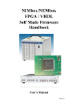
W-Ie–Ne-R
NIMbox/NEMbox
User’s Manual
*00Sachnummer.A0
General Remarks
The only purpose of this manual is a description of the product. It must not be interpreted as a declaration
of conformity for this product including the product and software.
W-Ie-Ne-R revises this product and manual without notice. Differences between the description in manual
and the product are possible.
W-Ie-Ne-R excludes completely any liability for loss of profits, loss of business, loss of use or data,
interrupt of business, or for indirect, special incidental, or consequential damages of any kind, even if
W-Ie-Ne-R has been advises of the possibility of such damages arising from any defect or error in this
manual or product.
Any use of the product which may influence health of human beings requires the express written
permission of W-Ie-Ne-R.
Products mentioned in this manual are mentioned for identification purposes only. Product names
appearing in this manual may or may not be registered trademarks or copyrights of their respective
companies.
No part of this product, including the product and the software may be reproduced, transmitted, transcribed,
stored in a retrieval system, or translated into any language in any form by any means without the express
written permission of W-Ie-Ne-R.
October 10
i
*00Sachnummer.A0
Table of contents:
1
Quick startup.............................................................................................................................. 1
1.1 Power up.............................................................................................................................................. 1
1.1.1 Important remark for NIMbox/NEMbox with ADCs (SU706)................................................... 1
1.2 Hardware detection and software installation ..................................................................................... 1
1.2.1 Windows...................................................................................................................................... 1
1.2.2 Linux ........................................................................................................................................... 2
1.3 Programming the FPGA...................................................................................................................... 2
2
Hardware description ................................................................................................................ 3
2.1 FPGAs ................................................................................................................................................. 3
2.2 General description of Nembox........................................................................................................... 3
2.3 I/O submodules ................................................................................................................................... 3
2.4 Hardware configuration....................................................................................................................... 4
2.5 SU703 – Discriminator I/O ................................................................................................................. 4
2.6 SU704 – NIM I/O................................................................................................................................ 5
2.7 SU706 – ADC submodule................................................................................................................... 6
2.7.1 Jumper settings at input stage...................................................................................................... 6
3
Software description .................................................................................................................. 7
3.1 USB communication ........................................................................................................................... 7
3.2 Addressing........................................................................................................................................... 8
3.3 Definining FPGA connections ............................................................................................................ 9
3.3.1 Reserved values:.......................................................................................................................... 9
3.4 Example Port Mapping (Front Panel) ................................................................................................. 9
3.5 Logic Pool for Labview™................................................................................................................. 10
3.5.1 DIO............................................................................................................................................ 10
3.5.2 Discriminator............................................................................................................................. 11
Logic...................................................................................................................................................... 12
3.5.4 Counter ...................................................................................................................................... 13
3.5.5 Gate Generator .......................................................................................................................... 13
3.5.6 LED ........................................................................................................................................... 13
3.6 Examples ........................................................................................................................................... 15
3.7 Usage of the ADCs............................................................................................................................ 18
3.7.1 ADC VI usage example............................................................................................................. 20
3.8 Usage of the DACs............................................................................................................................ 21
4
Advanced usage ....................................................................................................................... 22
4.1 Installing other firmwares provided by Wiener Plein & Baus .......................................................... 22
4.2 Installing self made firmwares .......................................................................................................... 22
5
Troubleshooting ....................................................................................................................... 22
5.1 Restoring the EEPROM .................................................................................................................... 22
October 10
ii
*00Sachnummer.A0
October 10
iii
*00Sachnummer.A0
User’s Manual
W-Ie–Ne-R
Nembox
Plein & Baus GmbH
1
Quick startup
1.1
Power up
On power up, the power LEDs are active and, if the firmware has been installed, the “BUSY”
LED will blink shortly. NIMbox/NEMbox is shipped with preinstalled firmware which is
consistent with the hardware version and with the position of the installed submodules on the
main FPGA board. Immediately after the first power up the USB communication is possible but
no configuration setup (or default configuration) is loaded within a couple of seconds. If the
user saves a configuration in the internal EEPROM, NIMbox/NEMbox loads the saved
configuration.
1.1.1 Important remark for NIMbox/NEMbox with ADCs (SU706)
Since a new connector has been added to each ADC channel to fully exploit the differential
capability of the ADC chip even with unipolar input connectors, in order to operate the ADC
with an unipolar input it is necessary to short-circuit the unused connector. A shorting plug is
needed for this operation.
Examples of operation with default configuration:
a) Positive signals:
- Insert the shorting plug in the first connector
- Connect the signal cable to the second connector
b) Negative signals:
- Connect the signal cable to the first connector
- Insert the shorting plug in the second connector
Wrong connections result in absence of signal or in wrong output values for peaks and charge
integrals in the FPGA.
1.2
Hardware detection and software installation
1.2.1 Windows
Once NIMbox/NEMbox has been powered and connected to a USB port, the hardware
installation wizard will guide the user through the installation steps. It is recommended not to let
Windows look for a proper driver. Choose instead to manually install the driver software from
the NIMbox/NEMbox package.
If the package drive is D, the driver directory is
D:\( NIMbox/NEMbox Version)\USB-Driver-FX2\
You may look for the driver files with the Hardware Manager of Windows or run the
installation script in the above directory.
After successful installation the user can verify the proper operation of NIMbox/NEMbox in the
Control Panel: in the Device Manager, there should be a new entry named DL7XX LogicBox.
Alternatively, the user can start the LabVIEW™ based programs IsNimboxThere.vi or
ListModules.vi, available in the package, which has a field for the NIMbox/NEMbox USB
address string and will return the NIMbox/NEMbox device ID if execution is successful.
IMPORTANT: the USB address string needed to identify NIMbox/NEMbox under
LabVIEW™ ¸can be found on a label on the backside of the module.
October 10
1
*00Sachnummer.A0
User’s Manual
W-Ie–Ne-R
Nembox
Plein & Baus GmbH
1.2.2 Linux
Please check www.wiener-d.com for updates.
1.3
Programming the FPGA
In order to quickly program the FPGA with predefined functionalities, it is recommended to use
LabVIEW™. Copy the NIMbox/NEMbox Logic Pool VIs from the NIMbox/Nembox package
to the VI user library directory of LabVIEW™.
For example:
copy from: D:\Labview 8.2\LogicPool to:
C:\Programs\National Instruments\LabVIEW 8.2\user.lib
Tests and Demos can be copied to an arbitrary directory.
By starting LabVIEW™ the new Logic Pool VIs will be available. These VIs are described in
this manual. By connecting the Logic Pool VIs and by starting your application, you will load a
configuration to the FPGA. This configuration will hold as long as you don’t overwrite it by
starting another application or as long as you don’t reset or swich off NIMbox/NEMbox. The
“close” VI will ask the user whether he wants to permanently save the configuration on the
internal EEPROM so that it won’ t be lost in case of power off..
When starting VIs for the first time it may be necessary to assist LabVIEW manually in
searching the path to DL700_FX2.dll.
October 10
2
*00Sachnummer.A0
User’s Manual
W-Ie–Ne-R
Nembox
Plein & Baus GmbH
2
Hardware description
2.1
FPGAs
A field-programmable gate array is a semiconductor device containing programmable logic
components and programmable interconnects. The programmable logic components can be
programmed to duplicate the functionality of basic logic gates such as AND, OR, XOR, NOT or
more complex combinational functions such as decoders or simple mathematical functions. In
most FPGAs, these programmable logic components (or logic blocks, in FPGA parlance) also
include memory elements, which may be simple flip-flops or more complete blocks of
memories.
An hierarchy of programmable interconnects allows the logic blocks of an FPGA to be
interconnected as needed by the system designer, somewhat like a one-chip programmable
breadboard. These logic blocks and interconnects can be programmed after the manufacturing
process by the customer/designer to implement any logical function—hence fieldprogrammable. However, this hardware programming is somewhat complex and requires
programming tools (for example VHDL) and considerable development effort. For this reason,
Nembox is shipped with a special software, Logic Pool, that provides the user with a large
number of preprogrammed function modules that are typically useful in signal processing.
2.2
General description of Nembox
Nembox is a programmable NIM module based on a FPGA board (DL706) with 4 slots for I/O
submodules that serve as interface between the FPGA I/O signals and the signals in the external
environment. It is equipped with a USB port for programming and read out and a connector for
direct FPGA programming/debugging.
Its 100 MHz clock makes Nembox well suited for processing signals with length down to 10 ns
and frequencies of several MHz. Such signals are common in nuclear and particle physics
applications, where NIM and TTL standards are used for signal transmission and processing.
NIMbox can be used for several application. Typical examples are ADC, discriminator, DAC,
NIM/TTL logic, trigger implementations, gate generation and data acquisition.
2.3
I/O submodules
Presently, the following submodules are available for Nembox:
Table 1: Nembox I/O submodules.
Submodule
SU700
SU701
SU703
SU704
SU705
SU706
SU707
SU709
SU710
SU711
SU712
SU713
October 10
Function
5x TTL I/O – LEMO COAX
16x TTL I/O – differential connector
4x Discriminator and 1x TTL I/O – LEMO COAX
5x NIM/TTL I/O – LEMO COAX
16 MByte RAM
1x ADC (100 Mhz) ,2x TTL I/O – LEMO COAX
8 x LVDS I/O
8 x Temperaturesensor
2x Fast DAC (100 Mhz)
6 x programmable Delayline 0,5ns .. 128 ns
16 x ADC (5 us, 14 Bit)
16 x DAC (14 Bit)
3
*00Sachnummer.A0
User’s Manual
W-Ie–Ne-R
Nembox
Plein & Baus GmbH
2.4
Hardware configuration
The slots for submodules in the main FPGA board are named MOD0, MOD1, MOD2 and
MOD3 counting top to bottom. For example, in the NDL8 version (see Wiener product catalog)
two slots are occupied by SU703s (discriminator) and two by SU704s (NIM/TTL I/O).
Please note that the preinstalled firmware depends on the ex works hardware configuration,
therefore only advanced users should consider removing, substituting or swapping submodules,
because this operation requires firmware reprogramming.
2.5
SU703 – Discriminator I/O
SU703 has 1 to 4 discriminator inputs and 4 to 1 TTL I/O ports, where the total sum of the
devices is limited to 5, i.e. the number of LEMO COAX connectors on the front. The first
LEMO connector corresponds always to a discriminator, while the last one always to a TTL I/O
port. Connectors 2 to 4 are discriminators by default but their functionality can be changed with
minor hardware modifications.
Discriminators thresholds can be programmed within the –2,5 / +2,5 V range and discriminators
hystereses within the 0 / 60 mV range, both with 12 bit resolution. High hysterese values are
used to prevent multiple threshold crossing (and thus multiple signal generation) due to noise.
The propagation delay is 3-4 ns and the maximum input frequency is 100 MHz.
The LEDs can be programmed independently from the I/O ports and a 10 ms stretcher is applied
in order to make short signals visible.
TTL I/Os can generate a current of more than 60 mA and therefore a sufficient TTL level >3V
with a 50 Ohm terminated coaxial line. If used as inputs, TTL I/Os must be terminated with 50
Ohm. Alternatively, it is possible to bring the input port high through a pull up resistor of about
1 kOhm, and through a simple switch it is possible to bring it down by shorting.
Table 2: SU703 (discriminator) pin assignments.
Pin N.
1
2
3
4
5
6
7
8
9
10
11
12
13
14
15
16
17
18
19
20
21
22
23
October 10
Function
+5V
+5V
COUT_4_p (discr. out, ch. 4, positive)
COUT_4_n (discr. out, ch. 4, negative)
COUT_3_p (discr. out, ch. 3, positive)
COUT_3_n (discr. out, ch. 3, negative)
COUT_2_p (discr. out, ch. 2, positive)
COUT_2_n (discr. out, ch. 2, negative)
COUT_1_p (discr. out, ch. 1, positive)
COUT_1_n (discr. out, ch. 1, negative)
SDI (serial data)
SCLK (serial clock)
LDAC_n (load DAC)
CS_TH_n (select threshold)
CS_HYS_n (select hysterese)
IN1 (TTL in, ch. 1)
IN2 (TTL in, ch. 2)
IN3 (TTL in, ch. 3)
OUT_4 (TTL out, ch. 4)
OE_4_n (enable TTL out, ch. 4, low active)
OUT_3 (TTL out, ch. 3)
OE_3_n (enable TTL out, ch. 3, low active)
OUT_2 (TTL out, ch. 2)
4
*00Sachnummer.A0
User’s Manual
W-Ie–Ne-R
Nembox
Plein & Baus GmbH
24
25
26
27
28
29
30
31
32
33
34
35
36
2.6
OE_2_n (enable TTL out, ch. 2, low active)
OUT_1 (TTL out, ch. 1)
OE_1_n (enable TTL out, ch. 1, low active)
LED3
LED4
LED1
LED2
LED5
IN4 (TTL in, ch. 4)
GND
GND
SU704 – NIM I/O
SU704 has 5 identical LEMO COAX I/O connectors to be used as programmable digital I/O
ports. Every I/O port supports both NIM and TTL levels, but the selected level is defined by a
jumper setting on the SU704 board (default level is NIM). Input impedance can be set to 50
Ohm through a relais.
Every NIM output can draw a current of -16mA, thus with a 50 Ohm impedance the level is 0,8V. The corresponding input threshold, with 50 Ohm set, is -0,4V. Maximum frequency is
100 MHz and propagation delay less than 4 ns.
Table 3: SU704 (NIM I/O) pin assignments.
Pin N.
1
2
3
4
5
6
7
8
9
10
11
12
13
14
15
16
17
18
19
20
21
22
23
24
25
October 10
Function
+ 5V
+5V
INTTL5 (TTL in, ch. 5)
OUT5 (NIM/TTL out, ch. 5)
INECL5 (NIM in, ch. 5)
ENA5 (enable TTL out, ch. 5, low active)
LED5
REL5 (relais 5)
INTTL4 (TTL in, ch. 4)
OUT4 (NIM/TTL out, ch. 4)
INECL4 (NIM in, ch. 4)
ENA4 (enable TTL out, ch. 4, low active)
LED4
REL4 (relais 4)
INTTL3 (TTL in, ch. 3)
OUT3 (NIM/TTL out, ch. 3)
INECL3 (NIM in, ch. 3)
ENA3 (enable TTL out, ch. 3, low active)
LED3
REL3 (relais 3)
INTTL2 (TTL in, ch. 2)
OUT2 (NIM/TTL out, ch. 2)
INECL2 (NIM in, ch. 2)
ENA2 (enable TTL out, ch. 2, low active)
LED2
5
*00Sachnummer.A0
User’s Manual
W-Ie–Ne-R
Nembox
Plein & Baus GmbH
26
27
28
29
30
31
32
33
34
35
36
2.7
REL2 (relais 2)
INTTL1 (TTL in, ch. 1)
OUT1 (NIM/TTL out, ch. 1)
INECL1 (NIM in, ch. 1)
ENA1 (enable TTL out, ch. 1, low active)
LED1
REL1 (relais 1)
GND
GND
SU706 – ADC submodule
2.7.1 Jumper settings at input stage
Since the 3rd generation of SU706 (september 2009) a new input connector has been added to
SU706. Since the signal applied internally to the ADC input is differential while the input
connectors are unipolar, with a second connector it is possible to preprocess data with the same
FPGA algorythm for negative and positive signals. In other words, it is possible to exploit the
differential capability to invert the singal by swapping connector. However, the connector where
no signal is applied must be shorted, either externally or (from trained staff) internally through
jumpers.
The default jumper settings in the input circuitry behind the ADC connectors (left) is as follows:
By default JX1 and JX2 are set to 1-2.
October 10
6
*00Sachnummer.A0
User’s Manual
W-Ie–Ne-R
Nembox
Plein & Baus GmbH
3
Software description
3.1
USB communication
The Nembox USB interface provides a number of commands for communicating with the
system or with the submodules. All commands are „byte oriented“ and identified by an ASCII
character. Addresses and data (1 to 4 bytes) are binary and the sequence of word and longword
transfers is big endian (most significant bytes first).
Table 4: System.
Command
Send
#
Receive
Function
4 Bytes
Send ID 31..0
R
System Reset
Table 5: Transfer.
Command
Send
Receive
Function
A
4 bytes
set address pointer A31..0
E
3 bytes
set address pointer A23..0
M
2 bytes
set address pointer A15..0
S
1 byte
set address pointer A7..0
A
4 bytes
read address pointer A31..0
+
increase address pointer A31..0 by 1
-
lower address pointer A31..0 by 1
N
2 bytes
set counter N15..0 for block transfer (A
autoincr)
F
2 bytes
set counter N15..0 for FIFO transfer (A)
L
N*4 bytes
write N longword(s)(A) (*)
L
T
N*4 bytes
N* 3 bytes
T
W
B
write N Triple(s)(A) (*)
N* 3 Bytes read N Triple(s)(A) (*)
N* 2 Bytes
W
B
read N longword(s)(A) (*)
write N Word(s)(A) (*)
N* 2 Bytes read N Word(s)(A) (*)
N* 1 Byte
write N Byte(s)(A) (*)
N* 1 Byte
read N Byte(s)(A) (*)
(*) Block transfers:
In case the block transfer counter N (commands ‚N’ and ‚F’) is set to1, a corresponding 1 byte
transfer according to the selected datawidth is executed.
October 10
7
*00Sachnummer.A0
User’s Manual
W-Ie–Ne-R
Nembox
Plein & Baus GmbH
When N > 1, N read or write cycles are executed and in case the counter was set with the ‚N’
command, the address pointer is incremented at each transfer. In case the command ‚F’ is used,
all transfers are executed at the same address (typ. FIFO).
The counter N after a block transfer is always set to 1, the address pointer A is resetted to the
start address.
CRC Check: (not yet available. Status: 14.6.2007)
Command
Send
Receive
Function
?
B0
send CRC checksum of all bytes sent
!
B0
send CRC checksum of all bytes received
Example sequence (Number format in HEX; ‚’=ASCII):
Sent
Received
Function
‚#’
00000100
ID number of the module=256
‚A’00000001
set address pointer A=1
‚S’0A
set address pointer A=10
‚a’
0000000A
‚L’00000200
write to current address (A=10) the 32Bit value=512
‚B’FF
write the byte value=255 to the addresse A=10
‚w’
02FF
read the value 767 from addresse A=10
‚+’
increase the address counter by 1 (A=11)
‚W’0304
write the value 772 to A=11
‚N’0002
set block transfer counter (Autoincr) to 2
‚-’
set address counter back to A=10
‚b’
3.2
read address pointer
FF04
block transfer of 2 bytes with auto increment
Addressing
All Logic Pool modules are addressed through a 24 bit address:
Address bits
Value range
A31..A24
Function
irrelevant
A23..A16
0..255
type address of a Logic Pool module (e.g. „T“, „L“,...)
A15..A8
1..255
Module address of a Logic Pool module
A7..A0
0..255
sub address for arbitrary parameters
Every module must notify his presence to subaddress=0 with a byte 0..254. If no module is
present at a specific address, the value 255 (or FF) is returned. Therefore an application (e.g.
October 10
8
*00Sachnummer.A0
User’s Manual
W-Ie–Ne-R
Nembox
Plein & Baus GmbH
OPEN in LabVIEW) can check that all modules are available and create a table of modules and
addresses.
All other module parameters on further sub addresses are specific for each module. The width of
the data word is arbitrary, between 1 and 4 bytes.
3.3
Definining FPGA connections
Each module has typically one or more signal inputs and outputs.
Every output (MUX_) has a specific connection value, that can be read out by every module.
Moreover, the logic state (STATE_) at output can be inquired at any time. Usually these values
are stored on the read-subaddresses 0..n .
Every input (_MUX) is outfitted with a multiplexer switch, that allows to set up the connection
to any output. Therefore any arbitrary interconnection between modules becomes possible. The
multiplexer are set to the user defined connection through a value in a register. Typically, the
input multiplexer values are written from the user to the write-subadresses 0..n .
Example: the output of the module T10 should be directed to the input of moduls I3
The command ‚E’’T’0A00’b’ delivers the connection value = 02.
Hence, the command ‚E’’I’0300’B’02 connect the signal as intended.
3.3.1 Reserved values:
By setting the MSB (most significant bit) of the multiplexer register, it is possible to invert
every input without using other resources (z.B.: ‚E’’I’0300’B’82).
3.4
•
Value 0 characterizes an open (not connected) input or output.
•
Value 127 produces a short trigger pulse, after that it is set to 128 (not yet
implemented).
•
Value 128 corresponds to a constant LOW level.
•
Value 255 corresponds to a constant HIGH level.
Example Port Mapping (Front Panel)
In order to be able to assign a function to input / output ports by means of a software, we need
to assign them a number.
Let’s consider the DNAE version (SU703, SU704, SU706 and SU710) as example.
The 17 I/O ports of NIMbox/NEMbox DNAE version have a default assignment as follows:
NIMbox
D1
D2
NIM module
D3
D4
SU703
T1
top -> bottom
N2
N3
N4
N5
N6 A1+ A1-
SU704
SU706
T7
T8
E1+ E1- E2+
SU710
Table 6: Mapping of physical I/O ports on front panel
“T” indicates a programmable TTL I/O port, “A” an ADC input, “N” a NIM or TTL
programmable I/O port, “D” a discriminator input port and “E” a DAC output port. Please note
that in order to change a NIM I/O into a TTL I/O or viceversa, a hardware intervention is
needed: it is necessary to change the position of the corresponding jumper in SU704.
This labeling is very important in order to map the physical position of the I/O ports to the
corrisponding software identifiers. While using LabVIEW™ VIs, the integer number which is
part of the port label should be provided as input.
October 10
9
*00Sachnummer.A0
E2-
User’s Manual
Nembox
W-Ie–Ne-R
Plein & Baus GmbH
NIM and TTL I/O ports are identified sequentially in Labview, e.g. T1 corresponds to port 1, T2
to port 2… and N4 corresponds to port 8.
3.5
Logic Pool for Labview™
Logic Pool is a set of tools for programming the Nembox FPGA under Labview.
It consists of the following components:
•
Firmware
•
USB communication VI
•
Applications (VIs)
The firmware is preinstalled on Nembox and can only be modified by advanced users with
detailed hardware information. For example, the DNAE version is equipped with the following
FPGA resources:
•
1 x ADC to control the ADC inputs
•
3 x TTL I/O
•
5 x NIM or TTL I/O
•
8 x Logic
•
4 x Counter
•
10 x LED
•
1 x TDC
These resources are described in this chapter and each one has its corresponding application VI
for easy access. The USB communication VIs is a VI interface to the file DL7xx_FX2.dll
The application VIs implement the following functionalities:
•
DIO
•
DISCRIMINATOR
•
LOGIC
•
COUNTER
•
LED
•
TDC
•
ADC
•
DAC
In order to make it possible to use more than one Nembox instance at one, all VIs have the I/O
parameters “USB In” and “USB Out” that can be used to distinguish sessions. By using the
provided OPEN.vi instrument, the selected USB device will be stored in a local variable for
reference of all other modules. This simplifies wiring of the moduls for single NemboX setups.
3.5.1 DIO
October
Picture 1: 10
Digital I/O Virtual Instrument
10
*00Sachnummer.A0
User’s Manual
W-Ie–Ne-R
Nembox
Plein & Baus GmbH
This VI controls a physical NIM or TTL I/O port on Nembox.
“Function” can be set to
•
Connect (default and normally executed once initially)
•
Set IN (sets the output to True or False, overrides any connection to OUT)
•
Get OUT (returns the status of the port)
The “Params” cluster (provided by the user) is used to pass values to “Function”. For example,
it can be used to determine the level of the I/O port. This could be choosen between:
•
TTL High Imp.
•
TTL 50 Ohm
•
NIM Open
•
NIM 50 Ohm
•
A debounce value may cancel spurious or intermittent input signals
The “DIO” integer value (provided by the user) identifies the physical port.
For example, by choosing a TTL option for “Params” and the number 3 for “DIO”, the resulting
physical port will be the T3, i.e. the 4th (where the 1st is the uppermost and the 16th the
lowermost port).
The VI has an input (OUT, because it is used to feed the real output signal which will actually
be generated by Nembox) and an output (IN, because it is used to receive an input signal into
the Nembox).
DIO:
‚T’n
Bytes Read
Bytes Write
0
1
MUX_IN
1
OUT_MUX
1
1
STATE_IN
1
Debounce
2
1
1
Mode: termination (0), NIM(1)
Debounce:
=0: debouncing disabled
=1..255: debouncing with 1..255 ms enabled
3.5.2 Discriminator
The “DISCR” output can be connected to other logical function or to an output port.
“Function” can be set to
•
Connect (default)
•
Get DISCR (get the input status - True or False)
•
Write Threshold (set the DAC for the threshold)
•
Write Hysteresis (set the DAC for hysteresis)
By using the “Params” cluster, values for threshold and hysteresis can be set.
DISCRIMINATOR:
October 10
11
*00Sachnummer.A0
User’s Manual
W-Ie–Ne-R
Nembox
Plein & Baus GmbH
‚D’n
Bytes Read
Bytes Write
0
1
MUX_IN
2
Threshold
1
1
STATE_IN
2
Hysteresis
Threshold:
The threshold (-2.5V..+2.5V) for the analog input signal is set through a 12Bit DAC. The most
significant 4 bits determine the channel in each module.
Hysteresis:
The hysteresis (0..60mV) for the analog input signal is set through a 12Bit DAC. The most
significant 4 bits determine the channel in each module.
3.5.3 Logic
This set of VIs provides the basic logic functions.
LOGIC:
‚L’n
Bytes Read
Bytes Write
0
1
MUX_Out
1
A_MUX
1
1
STATE_Out
1
B_MUX
2
1
Mode
3
1
FF
Mode:
0: OR
1: AND
2: XOR
3: RS-FF
4: S-FF
5: D-FF
6: Differentiator
7: Differentiator (Start Asynchronously)
8: Synchronisator
9: Synchronisator (Start Asynchronously)
FF (Flip Flop):
0: FF is deleted
1..255: FF is set
October 10
12
*00Sachnummer.A0
User’s Manual
W-Ie–Ne-R
Nembox
Plein & Baus GmbH
3.5.4 Counter
This set of VIs can be used for counting (scalers) or to generate an arbitrary train of pulses.
COUNTER:
‚C’n
Bytes Read
Bytes Write
0
1
MUX_Out
1
A_MUX
1
1
STATE_Out
1
B_MUX
2
1..4
Counter
1
Mode, Clear Counter
3
1..4
Pulse marks, Clear Counter
..n
1..4
Pulse marks, Clear Counter
Mode:
0: COUNTER
1: PULSER
2: ASYNC PULSER
3.5.5 Gate Generator
This VI is a simplified version of the pulser and is used to generate a programmable gate when a
trigger (TRIG) fires.
3.5.6 LED
This VI is used to control the status of the LEDs. The integer “LED” determines which LED is
being programmed, according to
NIMbox
D1
D2
NIM module
D3
D4
SU703
October 10
T1
top -> bottom
N2
N3
N4
N5
N6 A1+ A1-
SU704
SU706
13
T7
T8
E1+ E1- E2+
SU710
*00Sachnummer.A0
E2-
User’s Manual
W-Ie–Ne-R
Nembox
Plein & Baus GmbH
Table 6.
LED:
‚I’n
0
Bytes Read
1
October 10
Bytes Write
0
1
14
LED_MUX
*00Sachnummer.A0
User’s Manual
W-Ie–Ne-R
Nembox
Plein & Baus GmbH
3.6
Examples
Basic application structure:
Digital I/O Port #1 is programmed as NIM input with 50 Ohm termination
Digital I/O Port #2 is programmed as NIM output without termination, digital I/O Port #3 is
programmed as TTL output (unlike the 50 Ohm, NIM and TTL levels are NOT software
selectable. Jumpers must be in the corresponding position).
October 10
15
*00Sachnummer.A0
User’s Manual
Nembox
W-Ie–Ne-R
Plein & Baus GmbH
Digital I/O port #1 is programmed as NIM input with 50 Ohm termination and is connected to
digital I/O port #2, which is programmed as NIM output without termination, and digital I/O
Port #3, which is programmed as TTL output. Examples of NIM and TTL levels are pictured.
The typical signal delay introduced by this simple circuit (and by ~1m cables for measurement)
between DIO #1 and DIO #2 or #3 is about 20ns.
Internal Clock #1, programmed with a frequency of 1000 Hz, is connected to output #2 (NIM
open, non terminated)
Digital I/O inputs #1 and #2, both NIM and with 50 ohm termination, are connected to the AND
logic gate #1. The output of the logic gate is sent to digital I/O #3 (NIM open)
October 10
16
*00Sachnummer.A0
User’s Manual
Nembox
W-Ie–Ne-R
Plein & Baus GmbH
Discriminator #1, programmed with a threshold of –100mV and an hysteresis of 30mV, is
connected to an internal inverter (NIM Logic: NIM TRUE corresponds to a negative voltage)
whose output is connected to digital I/O port #2 (NIM open, non terminated).
Discriminator #1, programmed with a threshold of 200mV and an hysteresis of 30mV, is
connected to Gate Generator #1, generating gates of 100 x 10ns (= 1us), whose output is
connected to digital I/O port #2 (TTL). 10ns is the internal clock period.
The typical minimum signal delay introduced by this simple circuit (and by ~1m cables for
measurement) between Discriminator #1 and DIO #2 is about 50ns.
In this sequence, digital I/O port #1 is programmed as NIM Input and connected to “Counter”
and “Trigger” inputs of internal Counter #1. Then, there is a waiting time of 5 seconds, and
afterwards the Counter #1 is read out. The output is sent to the Counter indicator, that indicates
how many signals were received from port #1 within the 5 seconds.
October 10
17
*00Sachnummer.A0
User’s Manual
Nembox
W-Ie–Ne-R
Plein & Baus GmbH
3.7
Usage of the ADCs
The ADCH VI is a fast 14 Bit ADC Module with max. 100 MHz sampling rate for recording of
selected pulse parameters based on the SU706 ADC plug-on.
SU706 is the 14 bit 100MHz sampling ADC module with AC coupled, bipolar input with 50
Ohms impedance.
The following picture 1 shows the block diagram and principle operation of the ADCH module.
Fig. 1: ADC block diagram
October 10
18
*00Sachnummer.A0
User’s Manual
Nembox
W-Ie–Ne-R
Plein & Baus GmbH
Figure 1: Labview documentation of ADC VI
The ADC circuit samples and converts contineoulsy the analog input Inp with the System clock
of 100 MHz. The 14 Bit data Data are compared in a comperator (>) with the Threshold
value. Based on the comparison result the output signals Discr as well as IntTrigger are set.
The dual-ported memory RAM stores the data depending on the value of WriteAddr. The
memory is limited to 1024 samples size. In order to realise slower sample rates the WriteAddr
value can be set dependent on the Divider parameter also with a lower frequency of 100
MHz/n.
TriggerCntrl recognizes an external (if wired) trigger ExtTrigger or is using the internally
generated IntTrigger signal considers the defined size of PreSamples and PostSamples for the
WriteAddr.
In the event of a trigger the control circuit first makes sure that the required number of
PreSamples is written into the memory RAM and then sets a trigger signal. Then the defined
number of PostSamples is written into the RAM. Once the writing into the memory is
completed the signal Running with be cleared.
This is normally the moment to read out the sampled data fromn the memory. For this purpose
the current address WriteAddr will be read and the ReadAddr (modulo 1024!) is set to
= WriteAddr – PostSamples - PreSamples
October 10
19
*00Sachnummer.A0
User’s Manual
W-Ie–Ne-R
Nembox
Plein & Baus GmbH
in order to start reading the data from the beginning of the recording. After reading the sampled
the memory can be used again for recodring data.
An additional functional block PulsParams determines independently and in real-time some
pulse characteristics which can be read-out in addition to the sampled data.
These characteristics refer to a pulse which is above the defined threshold as shown in the
following figure.
Fig. 2 Definition of pulse characteristics parameters
3.7.1 ADC VI usage example
In order to correctly read out the ADC with the provided Labview VIs, the typical sequence of
operations is:
1) Use ReadStatus to ask for overflow=TRUE and running=FALSE
2) Use ReadData to read the wave
3) Use WriteParamsAndClear to reset the ADC for the next trigger
Alternatively, the ADC vi can be used in histogramming mode (see parameters).
October 10
Figure 2: Labview test ADC VI screen shot
20
*00Sachnummer.A0
User’s Manual
Nembox
W-Ie–Ne-R
Plein & Baus GmbH
3.8
Usage of the DACs
Unless custom specific ex works settings are requested, the DAC outputs of SU710 consist of
two channels on 4 plugs. For each channel there are two plugs: the signal is generated with
positive and negative polarity on both plugs. Furthermore, for each channel one signal (either
positiv or negative) is amplified.
The DAC has a clock of 100MHz, therefore it is able to generate a new user defined voltage
every 10 ns.
The usage of the DACs is very simple: in order to obtain an analog signal, the user should
provide a vector describing the signal to DATA (within the Params argument) and connect a
start signal to TRIG. Divider option for lower frequencies and continuous mode option are
foreseen.
For every DAC channel there is a straight and an inverted output. One of these two outputs in
amplified in SU710.
Figure 3: Labview documentation of DAC
October 10
21
*00Sachnummer.A0
User’s Manual
Nembox
W-Ie–Ne-R
Plein & Baus GmbH
4
Advanced usage
4.1
Installing other firmwares provided by Wiener Plein & Baus
It is possible to install other firmwares than the default one, provided the hardware
configuration matches. Please contact Wiener Plein & Baus GmbH for information and to get
authorization in case your device is under guarantee.
FpgaUpdateTool can be used to install new firmwares via USB. The firmware must be in the
main directory of your local hard disk, e.g. c:\myFirmware.bit
Installations from other directories with special characters or from network drives may fail.
4.2
Installing self made firmwares
Wiener Plein & Baus GmbH may disclose hardware information to expert users and/or VHDL
programmers in order to program NIMbox/NEMbox to meet special requirements.
For writing and installing self made software, the IDE tool from Xilinx is highly recommended.
The user also needs to know which FPGA and which memory is used in the device, and which
are the pin assignments of its components, in order to find the correct libraries for new
applications and in order to correctly synthesize and build the firmwares.
Please contact Wiener Plein & Baus before reprogramming the device.
5
Troubleshooting
5.1
Restoring the EEPROM
Incorrect software usage, power supply interruptions or other events may result in EEPROM
corruption.
In case NIMbox/NEMbox no longer appears in your USB device list on the device manager,
please make sure at first that it is properly powered and connected. If it is impossible to
esthablish USB communication, it may be helpful to restore the EEPROM. Please follow these
steps:
a) contact Wiener Plein & Baus to get authorization to open NIMbox/NEMbox if it is
under guarantee
b) disconnect and open NIMbox/NEMbox
c) set the jumper close to the quarz oscillator, near the USB plug (see picture)
d) power and connect NIMbox/NEMbox, it will show up as new device
e) reinstall the drivers, run the “DL700_FX2_Install…” tool or request it at Wiener Plein
& Baus
f) disconnect NIMbox/NEMbox to remove the jumper
g) close NIMbox/NEMbox, power and connect
Warning: restoring the EEPROM deletes any saved configuration.
October 10
22
*00Sachnummer.A0
User’s Manual
Nembox
W-Ie–Ne-R
Plein & Baus GmbH
Figure 4: Location of the jumper to restore the EEPROM (red arrow on the lower right corner)
October 10
23
*00Sachnummer.A0
User’s Manual
Nembox
W-Ie–Ne-R
Plein & Baus GmbH
October 10
24
*00Sachnummer.A0