1
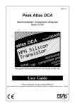
Intelligent Semiconductor Analyzer
User Manual
Please read this manual before switching the unit on.
Important safety information inside.
Intelligent Semiconductor Analyzer User Manual
2
Intelligent Semiconductor Analyzer User Manual
Page
Contents
1.Introduction ...........................................................................4
2.Important Considerations ......................................................5
3.Analysin Gsemiconductors......................................................6
3.3-1.Diodes...............................................................................6
3.3-2.Diodes Network............................................................... 7
3.3-3.LEDS.................................................................................8
3.3-4.Bicolour LEDS...................................................................9
3.3-5.Bipolar Junction Transistor................................................10
3.3-6.Transistor Special Features................................................11
3.3-7.Faulty or Very Low Gain Transistors...................................12
3.3-8.Current Gain (HFE)............................................................12
3.3-9.Base-Emitter Voltage Drop................................................13
3.3-10.Collector Leakage Current...............................................13
3.3-11.Mosfets...........................................................................14
3.3-12.Junction FETS Are conventional Field Effect Transistors...15
3.3-13.Thyristors........................................................................16
4.Battery Replacement................................................................17
3
Intelligent Semiconductor Analyzer User Manual
1.Introduction
Components tester is an intelligent semiconductor analyser that
offers great features together with refreshing simplicity. The Tester
brings a world of component data to your fingertips.
1.Automatic component type identification
•Bipolar transistors
•Darlington transistors
•Enhancement Mode MOSFETS
•Depletion Mode MOSFETS
•Junction FETS
•Low power sensitive Triacs
•Low power sensitive Thyristors
•Light Emitting Diodes
•Bicolour LEDS
•Diodes
•Diode networks
2.Automatic pinout identification, just connect any way round.
3.Special feature identification such as diode protection and resistor
3.shunts.
4.Gain measurement for bipolar transistors.
5.Leakage current measurement for bipolar transistors.
6.Silicon and Germanium detection for bipolar transistors.
7.Gate threshold measurement for Enhancement Mode Mosfets.
8.Semiconductor forward voltage measurement for diodes, LEDS and
3.transistor Base-Emitter junctions.
9.Automatic and manual power-off.
4
Intelligent Semiconductor Analyzer User Manual
2.Important Considerations
The Tester is designed to analyse discrete, unconnected, unpowered
components. This ensures that external connections don’t influence
the measured parameters. The three test probes can be connected
to the component any way round. If the component hasonly two
terminals, then any pair of the three test probes can be used.
The Tester will start component analysis when the ON/Analyse button
is pressed if the unit is powered down. If the Tester is not powered
down then a new analysis can be started by pressing and holding
the OFF/Page, button first to power down the unit and then pressing
the ON/Analyse button.
Depending on the component type, analysis may take a few seconds
to complete, after which, the results of the analysis are displayed.
Information is displayed a “page” at a time, each page can be displayed
by briefly pressing the OFF/Page button.
The arrow symbol on the display indicates that more pages are available
If the cannot detect any component
No Component
between any of the test probes, the
Detected
following message will be displayed:
If the component is not a supported
component type, a faulty component
or a component that is being tested
in-circuit, the analysis may result in the
following message being displayed:
Unknown/Faulty
Component
Some components may be faulty due
to a shorted junction between a pair
of the probes. If this is the case, the
following message (or similar) will be
displayed:
Short Circuit On
Green Blue
If all three probes are shorted (or very
low resistance) then the following
message will be displayed:
Short Circuit On
Green Blue Red
5
Intelligent Semiconductor Analyzer User Manual
It is possible that the Tester may detect one or more diode junctions
or other component type within an unknown or faulty part.
This is because many semiconductors comprise of PN (diode) junctions.
Please refer to the section on diodes and diode networks for more
information.
3.Analysin Gsemiconductors
3-1.Diodes
The Tester will analyse almost any type of diode. Any pair of the three
test clips can be connected to the diode, any way round. If the unit
detects a single diode, the following message will be displayed:
Pressing the OFF/Page button will then
display the pinout for the diode. In
this example, the Anode of the diode
is connected to the Red test clip and
the Cathode is connected to the Green
test clip, additionally, the Blue test clip
is unconnected. The forward voltage
drop is then displayed, this gives an
indication of the diode technology. In
this example, it is likely that the diode
is a silicon diode. A germanium or
Schottky diode may yield a forward
voltage of about 0.25V. The current at
which the diode was tested is also
displayed.
Diode Or Diode
Junction(s)
Red Green Blue
Anod Cath
Forward Voltage
Vf=0.64V
Test Current
If=4.38mA
The Tester will determine that the diode(s) under test is an LED
if the measured forward voltage drop exceeds 1.50V. Please refer to
the section on LED analysis for more information.
6
Intelligent Semiconductor Analyzer User Manual
3-2.Diodes Network
The Tester will intelligently identify popular types of three terminal
diode networks. For three terminal devices such as SOT-23 diode
networks, the three test clips must all be connected, any way round.
The instrument will identify the type of diode network and then
display information regarding each detected diode in sequence. The
following types of diode networks are automatically recognised by
the Tester:
Both cathodes connected together,
such as the BAV70 device.
Common Cathode
Diode Network
Anodes of each diode are connected
together, the BAW56W is an example.
Common Anode
Diode Network
Here, each diode is connected in series.
An example is the BAV99.
Following the component identification,
the details of each diode in the network
will be displayed.
Firstly, the pinout for the diode is displayed,
followed by the electrical information,
forward voltage drop and the current
at which the diode was tested. The
value of the test current depends on
the measured forward voltage drop
of the diode.
Series diode
network
Pinout for D1...
Red Green Blue
Anod Cath
Forward Voltage
D2 Vf=0.64V
Following the display of all the details for the first diode, the details
of the second diode will then be displayed.
7
Intelligent Semiconductor Analyzer User Manual
3-3.LEDS
An LED is really just a another type of diode, however, the Tester will
determine that an LED or LED network has been detected if the
measured forward voltage drop is larger than 1.5V. This also enables
the Tester to intelligently identify bicolour LEDs, both two-terminal
and three-terminal varieties.
Like the diode analysis, the pinout, the
forward voltage drop and the associated
test current is displayed.
Led Or Diode
Junction(s)
Here, the Cathode (-ve) LED terminal is
connected to the Green test clip and
the Anode (+ve) LED terminal is connected
to the Blue test clip.
Red Green Blue
Cath Anod
In this example, a simple green LED
yields a forward voltage drop of 1.87V.
Forward Voltage
Vf=1.87V
The test current is dependant on the
forward voltage drop of the LED, here
the test current is measured as 3.15mA.
Test Current
If=3.15mA
Some blue LEDS (and their cousins, white LEDS) require high forward
voltages and may not be detected by the Tester.
8
Intelligent Semiconductor Analyzer User Manual
3-4.Bicolour LEDS
Bicolour LEDS are automatically identified. If your LED has 3 leads
then ensure they are all connected, in any order.
A two terminal bicolour LED consists of two LED chips which are
connected in inverse parallel within the LED body. Three terminal
bicolour LEDS are made with either common anodes or common
cathodes.
Here a two terminal LED has been
detected.
Two Terminal
Bicolour LED
This message will be displayed if the
unit has detected a three terminal LED.
Three Terminal
Bicolour LED
The details of each LED in the package
will then be displayed in a similar way
to the diode networks detailed earlier.
Pinout for D1...
The pinout for the 1st LED is displayed.
Remember that this is the pinout for just
one of the two LEDS in the package.
Red Green Blue
Anod Cath
Interestingly, the voltage drops for each
LED relate to the different colours within
the bicolour LED. It may therefore be
possible to determine which lead is
connected to each colour LED within
the device. Red LEDs often have the
lowest forward voltage drop, followed
by yellow LEDS, green LEDs and finally,
blue LEDS.
Forward Voltage
D1 Vf=1.98V
Test Current
9
Intelligent Semiconductor Analyzer User Manual
3-5.Bipolar Junction Transistor
Bipolar Junction Transistors are simply "conventional" transistors,
although variants of these do exist such as Darlingtons, diode protected,
resistor shunted types and combinations of these types. All of these
variations are automatically identified by the Tester.
Bipolar Junction Transistors are available
in two main types, NPN and PNP. In
this example, the unit has detected a
Silicon PNP transistor.
The unit will determine that the
transistor is Germanium only if the
base-emitter voltage drop is less than
0.4V and is also PNP.
If the device is a Darlington transistor
(two BJTs connected together), the unit
will display a similar message to this:
PNP Silicon
Transistor
PNP Germanium
Transistor
NPN Darlington
Transistor
Pressing the OFF/Page button will result
in the transistor's pinout being displayed.
Here, the instrument has identified that
the Base is connected to the Red test
clip, the Collector is connected to the
Green test clip and the Emitter is
connected to the Blue test clip.
10
Red Green Blue
Base Coll Emit
Intelligent Semiconductor Analyzer User Manual
3-6.Transistor Special Features
Many modern transistors contain additional special features. If the
Tester has detected any special features, then the details of these
features are displayed next after pressing the OFF/Page button. If
there are no special features detected then the next screen will be
the transistor’s current gain.
Some transistors, particularly CRT
Diode Protection
deflection transistors and many large
Darlingtons have a protection diode
Between C-E
inside their package connected between
the collector and emitter.
The Philips BU505DF is a typical example of a diode protected bipolar
transistor. Remember that protection diodes are always internally
connected between the collector and the emitter so that they are
normally reverse biased.
For NPN transistors, the anode of the diode is connected to the emitter
of the transistor. For PNP transistors, the anode of the diode is
connected to the collector of the transistor.
Additionally, many Darlingtons and a few non-Darlington transistors
also have a resistor shunt network between the base and emitter of
the device.
The Tester can detect the resistor shunt if it has a resistance of typically
less than 60kΩ.
The popular Motorola TIP110 NPN Darlington transistor contains
internal resistors between the base and emitter.
When the unit detects the presence
of a resistive shunt between the base
and emitter, the display will show:
Additionally, the Tester will warn you
that the accuracy of gain measurement
(HFE) has been affected by the shunt
resistor.
Resistor Shunt
Between B-E
HFE Not Accurate
Due To B-E Res
11
Intelligent Semiconductor Analyzer User Manual
3-7.Faulty or Very Low Gain Transistors
Faulty transistors that exhibit very low
gain may cause the Tester to only identify
one or more diode junctions within
the device. This is because NPN transistors
consist of a structure of junctions that
behave like a common anode diode
Common Anode
network. PNP transistors can appear
Diode Network
to be common cathode diode networks.
The common junction represents the
base terminal. This is normal for situations
where the current gain is so low that
it is immeasurable at the test currents
used by the Tester.
In some circumstances, the unit may
not be able to deduce anything sensible
from the device at all, in which case
you will see either of these messages
Unknown/Faulty
Component
No Component
Detected
3-8.Current Gain (HFE)
The DC current gain (HFE) is displayed after any special transistor
features have been displayed.
The gain of all transistors can vary
considerably with collector current,
collector voltage and also temperature.
The displayed value for gain therefore
may not represent the gain experienced
at other collector currents and voltages.
This is particularly true for large devices.
Current Gain
HFE=119
Test Current
Ic=2.50mA
Darlington transistors can have very high gain values and more
variation of gain will be evident as a result of this.
Additionally, it is quite normal for transistors of the same type to
have a wide range of gain values. For this reason, transistor circuits
are often designed so that their operation has little dependence on
12
Intelligent Semiconductor Analyzer User Manual
the absolute value of current gain.
The displayed value of gain is very useful however for comparing
transistors of a similar type for the purposes of gain matching or
fault finding.
3-9.Base-Emitter Voltage Drop
The DC characteristics of the base-emitter junction are displayed,
both the base-emitter forward voltage drop and the base current
used for the measurement.
The forward base-emitter voltage drop
can aid in the identification of silicon
or germanium devices. Germanium
devices can have base-emitter voltages
as low as 0.2V, Silicon types exhibit
readings of about 0.7V and Darlington
transistors can exhibit readings of
about 1.2V because of the multiple
base-emitter junctions being measured.
B-E Voltage
Vbe=0.72V
Test Current
IB=4.48mA
3-10.Collector Leakage Current
The collector current that takes place when no base current is flowing
is referred to as Leakage Current. Most modern transistor exhibit
extremely low values of leakage current, often less than 1µA, even
for very high collector-emitter voltages.
Older Germanium types however can
suffer from significant collector leakage
current, particular at high temperatures
(leakage current can be very temperature
dependant).
Leakage Current
IC=0.15mA
If your transistor is a Silicon type, you should expect to see a leakage
current of close to 0.00mA unless the transistor is faulty.
13
Intelligent Semiconductor Analyzer User Manual
3-11.Mosfets
Mosfet stands for Metal Oxide
Semiconductor Field Effect Transistor.
Like bipolar transistors, Mosfets are
available in two main types, N-Channel
and P-Channel. Most modern Mosfets
are of the Enhancement Mode type,
meaning that the bias of the gate-source
voltage is always positive (For N-Channel
types). The other (rarer) type of Mosfet
is the Depletion Mode type which is
described in a later section.
Enhancement Mod
N-Ch MOSFET
Mosfets of all types are sometimes known as Igfets, meaning Insulated
Gate Field Effect Transistor. This term describes a key feature of these
devices, an insulated gate region that results in negligible gate current
for both positive and negative gate-source voltages (up to the
maximum allowed values of course, typically ±20V).
The first screen to be displayed gives
information on the type of Mosfet
detected. Pressing OFF/Page will then
result in the pinout of the Mosfet being
displayed. The gate, source and drain
are each identified.
An important feature of a Mosfet is the
gate-source threshold voltage, the gatesource voltage at which conduction
between the source and drain starts.
The gate threshold is displayed following
the pinout information.
14
Red Green Blue
Gate Drn Srce
Gate Threshold
Vgs=3.47V
Test Current
Id=2.50mA
Intelligent Semiconductor Analyzer User Manual
The fairly rare Depletion Mode Mosfet is very similar to the conventional
Junction FET (JFET) except that the gate terminal is insulated from
the other two terminals. The input resistance of these devices can
typically be greater than 1000MΩ for negative and positive gate-source
voltages.
Depletion Mode devices are characterised
by the gate-source voltage required
to control the drain-source current.
Depletion Mode
N-CH Mosfet
Modern Depletion Mode devices are generally only available in
N-Channel varieties and will conduct current between it's drain and
source terminals even with a zero voltage applied across the gate
and the source. The device can only be turned completely off by
taking it's gate significantly more negative than it's source terminal,
say -10V. It is this characteristic that makes them so similar to
conventional Jfets.
Pressing OFF/Page will cause the
pinout screen to be displayed.
Red Green Blue
Drn Gate Srce
3-12.Junction FETS Are conventional Field Effect Transistors
The voltage applied across the gate-source terminals controls current
between the drain and source terminals. N-Channel Jfets require a
negative voltage on their gate with respect to their source, the more
negative the voltage, the less current can flow between the drain
and source.
Unlike Depletion Mode Mosfets, Jfets
have no insulation layer on the gate.
This means that although the input
resistance between the gate and source
P-Channel
is normally very high, the gate current
Junction FET
can rise if the semiconductor junction
between the gate and source or between
the gate and drain become forward
biased. This can happen if the gate
voltage becomes about 0.6V higher
15
Intelligent Semiconductor Analyzer User Manual
than either the drain or source terminals
for N-Channel devices or 0.6V lower
than the drain or source for P-Channel
devices.
The internal structure of Jfets is essentially
symmetrical about the gate terminal,
this means that the drain and source
terminals are indistinguishable by the
Tester. The JFET type and the gate
terminal are identified however.
Drain And Source
Not Identified
Red Green Blue
Gate
3-13.Thyristors
Sensitive low power thyristors (silicon Controlled Rectifiers-scrs) and
triacs that require gate currents and holding currents of less than
5mA can be identified and analysed with the Tester.
Thyristor terminals are the anode,
Sensitive Or Low
cathode and the gate. The pinout of
Power Thyristor
the thyristor under test will be displayed
Red Green Blue
on the next press of the OFF/Page button.
Gate Anod Cath
Triac terminals are the MT1, MT2 (MT
Sensitive Or Low
standing for main terminal) and gate.
Power Triac
MT1 is the terminal with which gate
current is referenced.
Red Green Blue
MT1 MT2 Gate
16
Intelligent Semiconductor Analyzer User Manual
4.Battery Replacement
Tester should provide many years of service if used in accordance
with this user guide. Care should be taken not to expose your unit
to excessive heat, shock or moisture. Additionally, the battery should
be replaced at least every 12 months to reduce the risk of leak damage.
If a low battery warning message
appears, immediate replacement of the
battery is recommended as measured
parameters may be affected. The unit
may however continue to operate.
Low Battery
The battery can be replaced by carefully opening the Tester by removing
the three screws from the rear of the unit. Take care not to damage
the electronics.
The battery should only be replaced with a high quality battery identical
to, or equivalent to an Alkaline GP23A or MN21 12V (10mm diameter
x 28mm length).
17
Intelligent Semiconductor Analyzer User Manual
Intelligent Semiconductor Analyzer User Manual
Rev.100505
Intelligent Semiconductor Analyzer User Manual