1
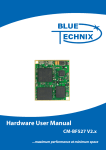
Hardware User Manual CM-BF527 v1.x Contact Bluetechnix Mechatronische Systeme GmbH Lainzerstraße 162/3 A-1130 Vienna AUSTRIA/EUROPE [email protected] http://www.bluetechnix.com Document No.: 100-1251-1.1 Document Revision 13 Date: 2010-07-12 Blackfin CM-BF527 Hardware User Manual 1 Table of Contents BLACKFIN Products ...................................................................................................................Error! Bookmark not defined. 1 2 Introduction .................................................................................................................................................................................. 7 1.1 Overview ............................................................................................................................................................................... 7 1.2 Key Features ........................................................................................................................................................................ 8 1.3 Target Applications ........................................................................................................................................................... 8 1.4 Further Information .......................................................................................................................................................... 8 Specification ................................................................................................................................................................................. 9 2.1 Functional Specification .................................................................................................................................................. 9 2.2 Boot Mode............................................................................................................................................................................ 9 2.3 Memory MAP .................................................................................................................................................................... 10 2.4 Electrical Specification .................................................................................................................................................. 11 2.4.1 Supply Voltage ....................................................................................................................................................... 11 2.4.2 Supply Voltage Ripple ......................................................................................................................................... 11 2.4.3 On Board Crystal Frequency .............................................................................................................................. 11 2.4.4 Real Time Clock Crystal........................................................................................................................................ 11 2.4.5 Supply Current ....................................................................................................................................................... 11 2.5 3 4 5 Environmental Specification ....................................................................................................................................... 11 2.5.1 Temperature ........................................................................................................................................................... 11 2.5.2 Humidity................................................................................................................................................................... 11 CM-BF527 .................................................................................................................................................................................... 12 3.1 Mechanical Outline ........................................................................................................................................................ 12 3.2 Footprint ............................................................................................................................................................................ 14 3.3 Schematic Symbol (Signals of X2 and X3) .............................................................................................................. 15 3.4 Connector Pin Assignments ........................................................................................................................................ 15 3.4.1 Connector X2 – (1-60) .......................................................................................................................................... 16 3.4.2 Connector X3 – (61-120) ..................................................................................................................................... 17 3.5 Reset circuit....................................................................................................................................................................... 19 3.6 RJ45 schematic ................................................................................................................................................................ 19 Software Support ..................................................................................................................................................................... 20 4.1 BLACKSheep ..................................................................................................................................................................... 20 4.2 uClinux ............................................................................................................................................................................... 20 Application Examples ............................................................................................................................................................. 21 5.1 Sample Schematic .......................................................................................................................................................... 21 Blackfin CM-BF527 Hardware User Manual 2 5.2 Stand-alone Ethernet based MPEG Webcam ........................................................................................................ 22 5.3 Design Services................................................................................................................................................................ 23 6 Anomalies ................................................................................................................................................................................... 24 7 Product Changes ...................................................................................................................................................................... 25 8 Production Report.................................................................................................................................................................... 25 8.1 9 10 CM-BF527 (100-1251) .................................................................................................................................................... 25 Document Revision History .................................................................................................................................................. 26 List of Figures and Tables.................................................................................................................................................. 27 Blackfin CM-BF527 Hardware User Manual 3 Edition 2008-09 © Bluetechnix Mechatronische Systeme GmbH 2008 All Rights Reserved. The information herein is given to describe certain components and shall not be considered as a guarantee of characteristics. Terms of delivery and rights of technical change reserved. We hereby disclaim any warranties, including but not limited to warranties of non-infringement, regarding circuits, descriptions and charts stated herein. Bluetechnix makes and you receive no warranties or conditions, express, implied, statutory or in any communication with you. Bluetechnix specifically disclaims any implied warranty of merchantability or fitness for a particular purpose. Bluetechnix takes no liability for any damages and errors causing of the usage of this board. The user of this board is responsible by himself for the functionality of his application. He is allowed to use the board only if he has the qualification. More information is found in the General Terms and Conditions (AGB). Information For further information on technology, delivery terms and conditions and prices please contact Bluetechnix (http://www.bluetechnix.com). Warning Due to technical requirements components may contain dangerous substances. The Core Modules and development systems contain ESD (electrostatic discharge) sensitive devices. Electro-static charges readily accumulate on the human body and equipment and can discharge without detection. Permanent damage may occur on devices subjected to high-energy discharges. Proper ESD precautions are recommended to avoid performance degradation or loss of functionality. Unused Core Modules and Development Boards should be stored in the protective shipping Blackfin CM-BF527 Hardware User Manual 4 BLACKFIN Products Core Modules: CM-BF533: Blackfin Processor Module powered by Analog Devices' single core ADSPBF533 processor; up to 600MHz, 32MB SDRAM, 2MB flash, 2x60 pin expansion connectors and a size of 36.5x31.5mm. CM-BF537E: Blackfin Processor Module powered by Analog Devices' single core ADSPBF537 processor; up to 600MHz, 32MB SDRAM, 4MB flash, integrated TP10/100 Ethernet physical transceiver, 2x60 pin expansion connectors and a size of 36.5x31.5mm. CM-BF537U: Blackfin Processor Module powered by Analog Devices' single core ADSPBF537 processor; up to 600MHz, 32MB SDRAM, 4MB flash, integrated USB 2.0 Device, 2x60 pin expansion connectors and a size of 36.5x31.5mm. TCM-BF537: Blackfin Processor Module powered by Analog Devices' single core ADSPBF537 processor; up to 500MHz, 32MB SDRAM, 8MB flash, a size of 28x28mm, 2x60 pin expansion connectors, Ball Grid Array or Border Pads for reflow soldering, industrial temperature range -40°C to +85°C. CM-BF561: Blackfin Processor Module powered by Analog Devices' dual core ADSPBF561 processor; up to 2x 600MHz, 64MB SDRAM, 8MB flash, 2x60 pin expansion connectors and a size of 36.5x31.5mm. CM-BF527: The new Blackfin Processor Module is powered by Analog Devices' single core ADSP-BF527 processor; key features are USB OTG 2.0 and Ethernet. The 2x60 pin expansion connectors are backwards compatible with other Core Modules. CM-BF548: The new Blackfin Processor Module is powered by Analog Devices' single core ADSP-BF548 processor; key features are 64MB DDR SD-RAM 2x100 pin expansion connectors. TCM-BF518: The new Core Module CM-BF518 is powered by Analog Devices' single core ADSP-BF518 processor; up to 400MHz, 32MB SDRAM, up to 8MB flash. The 2x60 pin expansion connectors are backwards compatible with other Core Modules. Development Boards: EVAL-BF5xx: Low cost Blackfin processor Evaluation Board with one socket for any Bluetechnix Blackfin Core Module. Additional interfaces are available, e.g. an SD-Card. DEV-BF5xxDA-Lite: Get ready to program and debug Bluetechnix Core Modules with this tiny development platform including an USB-Based Debug Agent. The DEVBF5xxDA-Lite is a low cost starter development system including a VDSP++ Evaluation Software License. DEV-BF548-Lite: Low-cost development board with one socket for Bluetechnix CM-BF548 Core Module. Additional interfaces are available, e.g. an SD-Card, USB and Ethernet. Blackfin CM-BF527 Hardware User Manual 5 DEV-BF548DA-Lite: Get ready to program and debug Bluetechnix CM-BF548 Core Module with this tiny development platform including an USB-Based Debug Agent. The DEV-BF548DA-Lite is a low-cost starter development system including a VDSP++ Evaluation Software License. EXT-Boards: The following Extender Boards are available: EXT-BF5xx-AUDIO, EXT-BF5xxVIDEO, EXT-BF5xx-CAM, EXT-BF5xx-EXP-TR, EXT-BF5xx-USB-ETH2, EXTBF5xx-AD/DA, EXT-BF548-EXP and EXT-BF518-ETH. Furthermore, we offer the development of customized extender boards for our customers. Software Support: BLACKSheep: The BLACKSheep VDK is a multithreaded framework for the Blackfin processor family from Analog Devices that includes driver support for a variety of hardware extensions. It is based on the real-time VDK kernel included within the VDSP++ development environment. LabVIEW: LabVIEW embedded support for Bluetechnix Core Modules is done by Schmid-Engineering AG: http://www.schmid-engineering.ch uClinux: All the Core Modules are fully supported by uClinux. The required boot loader and uClinux can be downloaded from: http://blackfin.uClinux.org. Upcoming Products and Software Releases: Keep up-to-date with all the changes to the Bluetechnix product line and software updates at: http://www.bluetechnix.com . Software Support: BLACKSheep: The BLACKSheep VDK is a multithreaded framework for the Blackfin processor family from Analog Devices that includes driver support for a variety of hardware extensions. It is based on the real-time VDK kernel included within the VDSP++ development environment. LabVIEW: LabVIEW embedded support for Bluetechnix Core Modules is done by Schmid-Engineering AG: http://www.schmid-engineering.ch uClinux: All the Core Modules are fully supported by uClinux. The required boot loader and uClinux can be downloaded from: http://blackfin.uClinux.org. Upcoming Products and Software Releases: Keep up-to-date with all the changes to the Bluetechnix product line and software updates at: http://www.bluetechnix.com BLACKFIN Design Service Based on more than five years of experience with Blackfin, Bluetechnix offers development assistance as well as custom design services and software development. Blackfin CM-BF527 Hardware User Manual 6 1 Introduction The CM-BF527 is a member of Blackfin based core modules incorporating the consumer temperature version of the ADSP-BF527 (optional also ADSP-BF525 or ADSP-BF522). It is backwards compatible to the CM-BF537E for most of its interfaces and can be used as a replacement module on any Bluetechnix development or evaluation Board. A special feature of this module is the on-board 10/100Mbit Ethernet interface which includes the physical transceiver chip and USB2.0 OTG Interface. The module allows easy integration into high demanding applications where space and power are very limited. 1.1 Overview The Core Module CM-BF527 consists of the following components: 60 Pin Expansion Connector B Dynamic Core Voltage Control 32 MByte SDRam USB2.0 OTG on BF527 8 MByte Flash Ethernet Physical BF527 600 MHz Low Voltage Reset 60 Pin Expansion Connector A Figure 1-1: Main components of the CM-BF527 Core Module Analog Devices Blackfin Processor ADSP-BF527 o ADSP-BF527KBCZ with 525MHz (* please see chapter8 for the correct part number) 32 MB SDRAM o SDRAM Clock up to 133MHz o MT48LC16M16A2BG-7 (16Mx16, 256Mbit at 3.3 V) 8 MB of Byte Addressable Flash o PF48F2000P0ZBQ0 (4Mx16, 64Mbit at 3.3V; addressable by 4 banks, 2Mb each, controlled over GPIOs) o Additional flash memory can be connected through the expansion board as parallel Flash using asynchronous chip select lines or as a SPI flash. Low Voltage Reset Circuit o Resets module if power supply goes below 2.93 V for at least 140 ms Blackfin CM-BF527 Hardware User Manual 7 1.2 o Allows adjusting of the core voltage by setting software registers on the Blackfin processor o Core voltage range: 0.8 – 1.2V Expansion Connector A o Data Bus o Address Bus o Control Signals o USB2.0 OTG o Ethernet Pins Expansion Connector B o PG (0..15) SPI, UART, SPORT, GPIO o JTAG o TWI (I2C compatible) o Power o PPI (Parallel Port Interface) , SPORT o Boot Mode o GPIO’s Key Features 1.3 The CM-BF527 is a low cost compact core module and measures only 36x31mm Allows quick prototyping of product that comes very close to the final design Reduces development costs, faster time to market Very cost effective for small and medium volumes Target Applications 1.4 Dynamic Core Voltage Control Mobile Embedded Device Generic high performance signal processor module Internet Connected Embedded System Industrial Control Further Information Further information, and document updates are http://www.bluetechnix.com/goto/cm-bf527 Blackfin CM-BF527 Hardware User Manual available on the product homepage: 8 2 Specification 2.1 Functional Specification Figure 2-1: Detailed Block Diagram Figure 2-1 shows a detailed block diagram of the CM-BF527 module. Besides the SDRAM control pins and the Pins used by the Ethernet Physical Transceiver (Port H) the CM-BF527 has all other pins of the Blackfin processor on its two main 60 pin connectors. A special feature of the CM-BF527 Core Module is the on-board physical Ethernet transceiver from Micrel (KSZ8721BLI). Dynamic voltage control allows reduction of power consumption to a minimum adjusting the core voltage and the clock frequency dynamically in accordance to the required processing power. A low voltage reset circuit guarantees a power on reset and resets the system when the input voltage drops below 2.93V. 2.2 Boot Mode By default the boot mode = 0000 (BMODE3 = low, BMODE2 = low, BMODE1 = low, BMODE0 = low). All BMODE pins have internal pull down resistors. Blackfin CM-BF527 Hardware User Manual 9 Switch Settings BM3,BM2,BM1,BM0 Boot Mode Description 0000 0001 0010 0011 0100 0101 0110 0111 1000 1001 1010 1011 1100 1101 1110 1111 0 (default) 1 2 3 4 5 6 7 8 9 10 11 12 13 14 15 Idle ‐ No bootReserved Boot from 8‐ or 16‐bit external flash memory Boot from 16‐bit asynchronous FIFO. Boot from serial SPI memory (EEPROM or flash) Boot from SPI host device Boot from serial TWI memory (EEPROM/flash) Boot from TWI host Boot from UART0 Host Boot from UART1 Host Reserved Boot from SDRAM Boot from OTP memory Boot from 8‐bit NAND flash via NFC using PORTF data pins Boot from 8‐bit NAND flash via NFC using PORTH data pins Boot from 16‐Bit Host DMA Boot from 8‐Bit Host DMA Table 2-1: Boot Mode CM-BF527 Connect BMODE0 to Vcc and leave BMODE1, BMODE2 and BMODE3 pins open for Boot Mode 0001 equals to 8 or 16 bit PROM/FLASH boot mode. This is the default boot mode of the BLACKSheep software and uClinux. Note: Boot Modes 8-15 are not supported with the DEV-BF5xx-DALite or EVAL-BF5xx 2.3 Memory MAP Memory Type Start Address End Address 1) FLASH PH9 Flag Low PG11 Flag Low FLASH 1) PH9 Flag High PG11 Flag Low FLASH 1) PH9 Flag Low PG11 Flag High FLASH 1) PH9 Flag High PG11 Flag High SD‐RAM Size Comment 0x20000000 0x201FFFFF 2MB ¼ of 8MB Flash, PF48F2000P0ZBQ0S 0x20000000 0x201FFFFF 2MB ¼ of 8MB Flash, PF48F2000P0ZBQ0S 0x20000000 0x201FFFFF 2MB ¼ of 8MB Flash, PF48F2000P0ZBQ0S 0x20000000 0x201FFFFF 2MB ¼ of 8MB Flash, PF48F2000P0ZBQ0S 0x00000000 0x01FFFFFF 32MB 16Bit Bus, Micron MT48LC16M16A2FG Table 2-2: Memory Map *) Please be aware that you have to unlock the flash before starting an erase process! The maximum amount of memory addressable by a single asynchronous memory bank, of the Blackfin processor is 2MB. In order to be able to use more than 2MB on a single bank, 2 GPIOs are used to select which 2MB section of flash is visible in the memory window of the Blackfin processor. This frees up the remaining banks for the user. Blackfin CM-BF527 Hardware User Manual 10 Please do not use the PH9 and PG11 pins as IO flags. You should leave these Pins disconnected! If one or both IO pins are needed and 4MB or 2 MB flash memory is sufficient for your application, remove the 0Ω resistors R26 and R19 from your Core Module. The flash address lines A20 and A21 are pulled Low. To access more than 8MB flash memory (64MB) you can add the 0Ω resistor array R2. But be aware to not connect the IO pins PG10, PG9 and PG1. Flash Address Pin Blackfin Flag CM Pin Number A20 A21 A22 A23 PH9 PG11 PG10 55 8 54 PG9 7 A24 PG1 39 Figure 2-2: IO pin to flash address pin assignment 2.4 Electrical Specification 2.4.1 Supply Voltage 3.3V DC +/-10% 2.4.2 Supply Voltage Ripple 100mV peak to peak 0-20 MHz 2.4.3 On Board Crystal Frequency 24 MHz: USB Clock 25 MHz: Blackfin Clock 2.4.4 Real Time Clock Crystal 32.768kHz 2.4.5 Supply Current 2.5 Maximum current: 350mA @3.3V Typical operating conditions: o Processor running at 600MHz, Core Voltage 1.2V, SDRAM 20% bandwidth utilization at 130MHz; Ethernet idle: 200mA @ 3.3V o Processor running at 300MHz, Core Voltage 0.8V SDRAM 20% bandwidth utilization at 130MHz; Ethernet idle: TBD o Processor running at 600MHz, Core Voltage 1.2V, SDRAM 20% bandwidth utilization at 130MHz, Ethernet TX/RX active: TBD Environmental Specification 2.5.1 Temperature Operating at full 600MHz: 0 to + 70° C 2.5.2 Humidity Operating: 10% to 90% (non condensing) Blackfin CM-BF527 Hardware User Manual 11 3 CM-BF527 3.1 Mechanical Outline TOP VIEW All dimensions are given in millimeters! Figure 3-1: Mechanical outline and Components on top side Take 0.5mm as a tolerance for the boarder of the board since it is broken out from a multi-board panel and some additional boarder may remain. The module is shipped with two 60pin connectors. Blackfin CM-BF527 Hardware User Manual 12 Figure 3-2: Side View with Connector mounted, 0.5mm tolerances The total minimum mounting height including receptacle at the motherboard is 6.1mm. Figure 3-3 shows the TOP VIEW of the bottom placed connectors (through the Board View) of the CMBF527 Core Module. All dimensions are given in millimeters! Figure 3-3: Mechanical outline and Bottom Connectors (top view) The mechanical outline represents a TOP VIEW of the connectors placed at the bottom of the core board. Blackfin CM-BF527 Hardware User Manual 13 Note the additional connector X1 (FFC-20) is not supported yet and used for AUDIO functionality in future revisions with the –C variant of the ADSP-BF527 Chip. X1 is not described in this document any further. The connectors on the CM-BF527 are of the following type: Part Manufacturer Manufacturer Part No. X2,X3 Hirose 3mm height FX8‐60P‐SV Table 3-1: Module connector types 3.2 Footprint For the baseboard the following connectors have to be used. Part Baseboard Manufacturer Manufacturer Part No. X2,X3 mating Hirose FX8‐60S‐SV Table 3-2: Baseboard connector types The footprint of the baseboard may look as shown in Figure 3-4. Figure 3-4: Recommended footprint of the Core Module (top view) Blackfin CM-BF527 Hardware User Manual 14 If there is no need to affix the Core Module, then you may omit the two M2 screwing holes. 3.3 Schematic Symbol (Signals of X2 and X3) U? 1 60 2 59 3 58 4 57 5 56 6 55 7 54 8 53 9 52 10 51 11 50 12 49 13 48 14 47 15 46 16 45 17 44 18 43 19 42 20 41 21 40 22 39 23 38 24 37 25 36 26 35 27 34 28 33 29 32 30 31 VppOTP A1 PH10/ND_CE/ERxD2/HOST_D10 A2 PH11/ND_WE/ETxD3/HOST_D11 A3 PH12/ND_RE/ERxD3/HOST_D12 A4 PH13/ND_BUSY/ERxCLK/HOST_D13 A5 PH14/ND_CLE/ERxDV/HOST_D14 A6 PH15/ND_ALE/COL/HOST_D15 A7 PG0/HWAIT A8 CLK_out A9 SCL A10 SDA A11 PH9/SPISEL5/ETxD2/HOST_D9/TACLK3 A12 PG9/TMR5/RSCLK0A/TACI5 A13 PG10/TMR6/TSCLK0A/TACI6 A14 PG11/TMR7/HOST_WR A15 USB_VBUS A16 Vin 3V3 A17 GND A18 Vin 3V3 A19 GND ABE0 PF0/PPI D0/DR0PRI /ND_D0A ABE1 PF1/PPI D1/RFS0/ND_D1A LED_SPEED PF2/PPI D2/RSCLK0/ND_D2A LED_ACT PF3/PPI D3/DT0PRI/ND_D3A LED_FD PF4/PPI D4/TFS0/ND_D4A/TACLK0 GND PF5/PPI D5/TSCLK0/ND_D5A/TACLK1 TX+ PF6/PPI D6/DT0SEC/ND_D6A/TACI0 RX+ PF7/PPI D7/DR0SEC/ND_D7A/TACI1 TXPF8/PPI D8/DR1PRI RXPF9/PPI D9/RSCLK1/SPI SEL6 VA25 PF10/PPI D10/RFS1/SPI SEL7 ARDY PF11/PPI D11/TFS1/CZM USB_OTG_ID PF12/PPID12/DT1PRI/SPISEL2/CDG USBD+ PF13/PPID13/TSCLK1/SPISEL3/CUD USBDPF14/PPI D14/DT1SEC/UART1TX SCLK PF15/PPID15/DR1SEC/UART1RX VDD-RTC PG6/DT0PRIA/TMR2/PPIFS3 GND PG5/TMR1/PPIFS2 AMS2 PPIFS1/TMR0 AMS3 PPIClk/TMRCLK ARE PPIFS1/TMR0 AWE PG12/DMAR1/UART1TXA/H_ACK AOE PG13/DMAR0/UART1RXA/H_ADR NMI PG1/SPISS/SPISEL1 RESET PG8/TMR4/RFS0A/UART0RX/TACI4 D0 PG7/TMR3/DR0PRIA/UART0TX D1 PG4/SPI MOSI/DT0SECA D2 PG3/SPI MISO/DR0SECA D3 PG2/SPISCK D4 Bmode1 D5 Bmode0 D6 Bmode3 D7 GND D8 Bmode2 D9 TCK D10 TDO D11 TDI D12 TMS D13 TRST D14 EMU D15 CM-BF527 61 120 62 119 63 118 64 117 65 116 66 115 67 114 68 113 69 112 70 111 71 110 72 109 73 108 74 107 75 106 76 105 77 104 78 103 79 102 80 101 81 100 82 99 83 98 84 97 85 96 86 95 87 94 88 93 89 92 90 91 CM‐BF527 Figure 3-5: Schematic Symbol of Module Note: For compatibility, some pin names appear twice on the connector. X1 is not supported yet and not shown in the symbol. 3.4 Connector Pin Assignments In the following tables you will find pin assignments for the Core Module connectors. Most pins are directly connected to the Blackfin processor. If not, please read the Notes below the table. Blackfin CM-BF527 Hardware User Manual 15 3.4.1 Connector X2 – (1-60) Please mind the mounted pull up and pull down resistors on the Core Module. See the third column of Table 3-3. Pin Signal Name No. Signal type 1 2 3 4 5 6 7 8 9 10 11 12 13 14 15 16 17 18 19 20 21 22 23 24 25 26 27 28 29 30 31 32 33 34 35 36 37 38 39 40 41 42 Power1) IO IO IO IO IO IO IO – 10k pull down Power Power IO IO IO IO IO IO IO IO IO IO IO IO IO IO IO I ‐ 10k pull down Power I ‐ 10k pull up I ‐ 10k pull up I ‐ 4k7 pull down O I – 10k pull up O I ‐10k pull down I ‐10k pull down I ‐10k pull down IO IO IO IO IO IO VppOTP PH11/ND_WE/ETxD3/HOST_D11 PH13/ND_BUSY/ERxCLK/HOST_D13 PH15/ND_ALE/COL/HOST_D15 CLKBUF SDA PG9 / RSCLK0A/ TMR5 / TACI5 DNU2) or PG11 / TMR7 / HOST_WR ˉˉˉˉˉˉˉˉˉ Vin 3V3 Vin 3V3 PF0 / PPID0 / DR0PRI / ND_D0A PF2 / PPI D2 / RSCLK0 / ND_D2A PF4 / PPI D4 / TFS0 / ND_D4A / TACLK0 PF6 / PPI D6 / DT0SEC / ND_D6A / TACI0 PF8 / PPID8 / DR1PRI PF10 / PPID10 / RFS1 / SPISEL7 ˉˉˉˉˉˉˉˉ PF12 / PPID12 / DT1PRI / SPISEL2 ˉˉˉˉˉˉˉˉ / CDG PF14 / PPID14 / DT1SEC / UART1TX PG6 / DT0PRIA / TMR2 / PPIFS3 PPIFS1 / TMR0 PPIFS1 / TMR0 PG13 / DMAR0 / UART1RXA / H_ADR / TACI2 PG8 / TMR4 / RFS0A / UART0RX / TACI4 PG4 / SPIMOSI / DT0SECA PG2 / SPISCK Bmode0 GND TCK TDI TRST ˉˉˉˉˉ EMU ˉˉˉˉ TMS TDO Bmode2 Bmode3 Bmode1 PG3 / SPIMISO / DR0SECA PG7 / TMR3 / DR0PRIA / UART0TX PG1 / SPISS ˉˉˉˉˉ / SPISEL1 ˉˉˉˉˉˉˉˉ PG12 / DMAR1 / UART1TXA / H_ACK PPICLK / TMRCLK PG5 / TMR1 / PPIFS2 Blackfin CM-BF527 Hardware User Manual 16 43 44 45 46 47 48 49 50 51 52 53 54 55 56 57 58 59 60 PF15 / PPID15 / DR1SEC / UART1RX / TACI3 PF13 / PPID13 / TSCLK1 / SPISEL3 ˉˉˉˉˉˉˉˉ / CUD PF11 / PPID11 / TFS1 / CZM PF9 / PPID9 / RSCLK1 / SPISEL6 ˉˉˉˉˉˉˉˉ PF7 / PPID7 / DR0SEC / ND_D7A / TACI1 PF5 / PPID5 / TSCLK0 / ND_D5A / TACLK1 PF3 / PPID3 / DT0PRI / ND_D3A PF1 / PPID1 / RFS0 / ND_D1A GND GND USB_VBUS PG10 / TMR6 / TSCLK0A / TACI6 DNU2) or PH9/SPISEL5 ˉˉˉˉˉˉˉˉ/ETxD2/HOST_D9/TACLK3 SCL PG0 / HWAIT PH14/ND_CLE/ERxDV/HOST_D14 PH12/ND_RE/ERxD3/HOST_D12 PH10/ND_CE/ERxD2/HOST_D10 IO IO IO IO IO IO IO IO Power Power I/O IO IO – 10k pull down O IO IO IO IO Table 3-3: Connector X2 pin assignment 1) Internally connected to 2.5V. If you want to program the OTP memory, just power this pin with 7.0V. 2) These IO pins are normally used to access more flash memory. They should not be used as general purpose IO pins. For more information please see chapter 2.3. 3.4.2 Connector X3 – (61-120) Please mind the mounted pull up and pull down resistors on the Core Module. See the third column of Table 3-4. Pin No. Signal Name Signal type 61 62 63 64 65 66 67 68 69 70 71 72 73 74 75 76 77 78 A1 A3 A5 A7 A9 A11 A13 A15 A17 A19 ABE1 ˉˉˉˉ LED_ACT GND RX+ RX‐ ARDY USBD+ SCLK O O O O O O O O O O O IO Power IO – 49R9 pull up to 2V5 IO – 49R9 pull up to 2V5 I I/O O Blackfin CM-BF527 Hardware User Manual 17 79 80 81 82 83 84 85 86 87 88 89 90 91 92 93 94 95 96 97 98 99 100 101 102 103 104 105 106 107 108 109 110 111 112 113 114 115 116 117 118 119 120 GND AMS3 ˉˉˉˉ AWE ˉˉˉ NMI ˉˉˉ D0 D2 D4 D6 D8 D10 D12 D14 D15 D13 D11 D9 D7 D5 D3 D1 RESET ˉˉˉˉˉ AOE ˉˉˉ ARE ˉˉˉ AMS2 ˉˉˉˉ VDD‐RTC USBD‐ USB_OTG_ID VA25 TX‐ TX+ LED_FD LED_SPEED ABE0 ˉˉˉˉ A18 A16 A14 A12 A10 A8 A6 A4 A2 Power O O I ‐10k pull up IO IO IO IO IO IO IO IO IO IO IO IO IO IO IO IO I/O see chapter 3.5 O O O Power I/O I Power Out IO – 49R9 pull up to 2V5 IO – 49R9 pull up to 2V5 IO IO O O O O O O O O O O Table 3-4: Connector X3 pin assignment Blackfin CM-BF527 Hardware User Manual 18 3.5 Reset circuit The reset of the flash and the processor are connected to a power monitoring IC. The output can be used as power on reset for external devices, see Figure 3-6. 3.3V RESET of Flash TCM809SENB713 3 VDD R12 2 RESET 1 RESET of ADSP-BF5xx 470R GND 100R U5 Core Module 99 GND External RESET Figure 3-6: Schematic of reset circuit on the Core Module 3.6 RJ45 schematic 7 24 The KSZ8721BLI is connected via the RMII to the processor. 3 4 5 6 9 10 11 22 21 2 1 48 30 VddPLL Vdd_CORE RxD3/PHYAD RxRxD2/PHYAD2 Rx+ RxD1/PHYAD3 FXSD/FXEN RxD0/PHYAD4 TxRx_DV/CRSDV/PCS_LBPK Tx+ Rx_CLK Rx_ER/ISO REXT CRS/RMII_BTB COL/RMII SPEED100/FEF COLLISION/NWAYEN MDC ACTIVITY/TEST MDIO FDUPLEX RESET CLKIN/XTAL1 38 31 42 2.5V_VA R2 49R9 R3 49R9 13 75 32 Rx‐ 33 34 40 41 Tx+ 76 107 108 LED_SPEED XTAL2 GND 6 5 4 3 2 1 D‐TVS‐USB2.0 V1 1 2 3 xRx‐ R4 GND xRx+ R5 3V3 27R 27R V2 4 5 6 xTx‐ 2.5V_VA xTx+ 3V3 D‐TVS‐USB2.0 R6 49R9 R7 49R9 C1 100n LED_ACT 2.5V_VA 110 R8 72 220R R9 46 PD INT/PHYAD0 2.5V_VA Rx+ Tx‐ 37 27 29 26 28 GND R1 10R 47 14 Vdd Vdd VddRCV VddRX VddTX 12 11 8 7 3 2 1 9 10 RdRd+ TdTd+ X1 RJ45 1:1 LED GND Taimag RJLBC-060TC1 GND 220R 45 8 12 23 35 36 39 43 44 GND GND GND GND GND GND GND GND 25 2.5V_VA KS8721 TxD3 TxD2 TxD1 TxD0 Tx_EN Tx_CLK/REFCLK Tx_ER/TXD4 13 U1 20 19 18 17 16 15 14 Core Module External GND Figure 3-7: Schematic for RJ45 Connection Designator Value Type Description Quantity X1 R4, R5 R8, R9 V1, V2 27R 220R RJLBC‐060TC1 RJ45 with transformer Resistor Resistor TSV‐Diode 1 2 2 2 USBLC6‐2P6 Table 3-5: Parts List RJ45 Blackfin CM-BF527 Hardware User Manual 19 4 Software Support 4.1 BLACKSheep The Core Module is delivered with a pre-flashed basic version of the BLACKSheep VDK multithreaded framework. It contains a boot-loader for flashing the Core Module via the serial port. The BLACKSheep for the CM-BF527 contains also a web server. By typing http://192.168.0.10 you can see a standard web page installed on the Core Module. Please consult the software development documents. 4.2 uClinux The Core Module is fully supported by the open source platform at http://blackfin.uclinux.org. Since the Core Modules are pre-flashed with BLACKSheep you have to flash uBoot first. To flash the uBoot you can use the BLACKSheep boot-loader. Blackfin CM-BF527 Hardware User Manual 20 5 Application Examples 5.1 Sample Schematic In this minimum configuration the CM-BF527 is used as a high performance network connected processor module. U1 ADP3338 3.3V 2 1 C1 1uF OUT P1 1uF C2 U2 GND 3.3V C3 10uF VIN-561 C4 GND1uF GND GND 3.3V 3.3V R3 4k7 P3 13 14 11 12 9 10 7 8 5 6 3 4 1 2 GND TCK TDO TDI TMS TRST EMU GND 1 60 2 59 3 58 4 57 5 56 6 55 7 54 8 53 9 52 10 51 11 50 12 49 13 48 14 47 15 46 16 45 17 44 18 43 19 42 20 41 21 40 22 39 23 38 24 37 25 36 26 35 27 34 28 33 29 32 30 31 VppOTP A1 PH10/ND_CE/ERxD2/HOST_D10 A2 PH11/ND_WE/ETxD3/HOST_D11 A3 PH12/ND_RE/ERxD3/HOST_D12 A4 PH13/ND_BUSY/ERxCLK/HOST_D13 A5 PH14/ND_CLE/ERxDV/HOST_D14 A6 PH15/ND_ALE/COL/HOST_D15 A7 PG0/HWAIT A8 CLK_out A9 SCL A10 SDA A11 PH9/SPISEL5/ETxD2/HOST_D9/TACLK3 A12 PG9/TMR5/RSCLK0A/TACI5 A13 PG10/TMR6/TSCLK0A/TACI6 A14 PG11/TMR7/HOST_WR A15 USB_VBUS A16 Vin 3V3 A17 GND A18 Vin 3V3 A19 CM-BF527 GND ABE0 PF0/PPI D0/DR0PRI /ND_D0A ABE1 PF1/PPI D1/RFS0/ND_D1A LED_SPEED PF2/PPI D2/RSCLK0/ND_D2A LED_ACT PF3/PPI D3/DT0PRI/ND_D3A LED_FD PF4/PPI D4/TFS0/ND_D4A/TACLK0 GND PF5/PPI D5/TSCLK0/ND_D5A/TACLK1 TX+ PF6/PPI D6/DT0SEC/ND_D6A/TACI0 RX+ PF7/PPI D7/DR0SEC/ND_D7A/TACI1 TXPF8/PPI D8/DR1PRI RXPF9/PPI D9/RSCLK1/SPI SEL6 VA25 PF10/PPI D10/RFS1/SPI SEL7 ARDY PF11/PPI D11/TFS1/CZM USB_OTG_ID PF12/PPID12/DT1PRI/SPISEL2/CDG USBD+ PF13/PPID13/TSCLK1/SPISEL3/CUD USBDPF14/PPI D14/DT1SEC/UART1TX SCLK PF15/PPID15/DR1SEC/UART1RX VDD-RTC PG6/DT0PRIA/TMR2/PPIFS3 GND PG5/TMR1/PPIFS2 AMS2 PPIFS1/TMR0 AMS3 PPIClk/TMRCLK ARE PPIFS1/TMR0 AWE PG12/DMAR1/UART1TXA/H_ACK AOE PG13/DMAR0/UART1RXA/H_ADR NMI PG1/SPISS/SPISEL1 RESET PG8/TMR4/RFS0A/UART0RX/TACI4 D0 PG7/TMR3/DR0PRIA/UART0TX D1 PG4/SPI MOSI/DT0SECA D2 PG3/SPI MISO/DR0SECA D3 PG2/SPISCK D4 Bmode1 D5 Bmode0 D6 Bmode3 D7 GND D8 Bmode2 D9 TCK D10 TDO D11 TDI D12 TMS D13 TRST D14 EMU D15 61 120 62 119 63 118 64 117 65 116 66 115 67 114 68 113 69 112 70 111 71 110 72 109 73 108 74 107 75 106 76 105 77 104 78 103 79 102 80 101 81 100 82 99 83 98 84 97 85 96 86 95 87 94 88 93 89 92 90 91 VA2.5V GND C5 100nF 13 IN GND P2 Tx+ Rx+ TxRx- GND VA2.5V 1 2 3 4 5 27 VA2.5V 6 R1 R2 27 8 GND 3.3V GND HALO HFJ11-2250E 14 3 GND 5.0V 1 2 3 GND RESET S1 SW_SMD * GND CM‐BF527 Header 7X2 JTAG Header Figure 5-1: Configuration with Ethernet and JTAG Connector Designator Value Type Description Quantity C1, C2, C4 C3 C5 P1 P2 P3 R1, R2 R3 S1 U1 U2 1uF 10uF 100nF 27 4k7 DC‐8 HFJ11‐2250E ADP3338 Capacitor Capacitor Capacitor Power connector DC‐8 RJ45 with transformer Header, 7‐Pin, dual row Resistor Resistor Switch Low dropout regulator CM‐BF537 3 1 1 1 1 1 2 1 1 1 1 Table 5-1: Bill of Material of Sample Schematic Blackfin CM-BF527 Hardware User Manual 21 5.2 Stand-alone Ethernet based MPEG Webcam The CM-BF527 module can be used as a stand-alone module for a camera system requiring only power supply and the direct attachment of a compatible video camera. An extender board including a camera is available at Bluetechnix (EXT-BF5xx-CAM). P1 1uF C6 GND CE Torex XC6204 3.3V U3 5 1 C2 1uF C3 1uF GND 3 1.3V VIN CE GND VOUT 5 C4 1uF ADJ 3 VOUT VSS C1 1uF 2.8V VIN 4 U2 1 ADJ 3.3V 2 2 1 C5 1uF OUT VSS GND IN 4 ADP3338 3.3V 3 2 U1 5.0V 1 2 3 Torex XC6204 GND GND GND GND U4 13 3 5 R2 220 10 11 4 PCLK VSYNC HREF 15 R3 10k 17 7 9 DVDD DOVDD AVDD CamCLK 3.3V PWDN RESET NC XCLK SIO_D SIO_C 10uF VIN-561 AGND GND DGND R1 10k 8 6 2.8V OV2640FSL 24 D0 23 D1 19 D2 21 D3 22 D4 20 D5 18 D6 16 D7 14 D8 12 D9 C8 GND 1uF GND PPI1D0 PPI1D1 PPI1D2 PPI1D3 PPI1D4 PPI1D5 PPI1D6 PPI1D7 PPI1D8 PPI1D9 PPI1D10 2 Cam1 GND PP13 GND PP15 PPI1Clk PP15 PF3 533 3.3V R6 10k 3.3V green PP13 DS1 TMR0 533 S2 SW_SMD R7 220 CM-BF527 61 120 62 119 63 118 64 117 65 116 66 115 67 114 68 113 69 112 70 111 71 110 72 109 73 108 74 107 75 106 76 105 77 104 78 103 79 102 80 101 81 100 82 99 83 98 84 97 85 96 86 95 87 94 88 93 89 92 90 91 VA2.5V GND C9 100nF 13 3.3V 1.3V 3.3V VppOTP A1 PH10/ND_CE/ERxD2/HOST_D10 A2 PH11/ND_WE/ETxD3/HOST_D11 A3 PH12/ND_RE/ERxD3/HOST_D12 A4 PH13/ND_BUSY/ERxCLK/HOST_D13 A5 PH14/ND_CLE/ERxDV/HOST_D14 A6 PH15/ND_ALE/COL/HOST_D15 A7 PG0/HWAIT A8 CLK_out A9 SCL A10 SDA A11 PH9/SPISEL5/ETxD2/HOST_D9/TACLK3 A12 PG9/TMR5/RSCLK0A/TACI5 A13 PG10/TMR6/TSCLK0A/TACI6 A14 PG11/TMR7/HOST_WR A15 USB_VBUS A16 Vin 3V3 A17 GND A18 Vin 3V3 A19 GND ABE0 PF0/PPI D0/DR0PRI /ND_D0A ABE1 PF1/PPI D1/RFS0/ND_D1A LED_SPEED PF2/PPI D2/RSCLK0/ND_D2A LED_ACT PF3/PPI D3/DT0PRI/ND_D3A LED_FD PF4/PPI D4/TFS0/ND_D4A/TACLK0 GND PF5/PPI D5/TSCLK0/ND_D5A/TACLK1 TX+ PF6/PPI D6/DT0SEC/ND_D6A/TACI0 RX+ PF7/PPI D7/DR0SEC/ND_D7A/TACI1 TXPF8/PPI D8/DR1PRI RXPF9/PPI D9/RSCLK1/SPI SEL6 VA25 PF10/PPI D10/RFS1/SPI SEL7 ARDY PF11/PPI D11/TFS1/CZM USB_OTG_ID PF12/PPID12/DT1PRI/SPISEL2/CDG USBD+ PF13/PPID13/TSCLK1/SPISEL3/CUD USBDPF14/PPI D14/DT1SEC/UART1TX SCLK PF15/PPID15/DR1SEC/UART1RX VDD-RTC PG6/DT0PRIA/TMR2/PPIFS3 GND PG5/TMR1/PPIFS2 AMS2 PPIFS1/TMR0 AMS3 PPIClk/TMRCLK ARE PPIFS1/TMR0 AWE PG12/DMAR1/UART1TXA/H_ACK AOE PG13/DMAR0/UART1RXA/H_ADR NMI PG1/SPISS/SPISEL1 RESET PG8/TMR4/RFS0A/UART0RX/TACI4 D0 PG7/TMR3/DR0PRIA/UART0TX D1 PG4/SPI MOSI/DT0SECA D2 PG3/SPI MISO/DR0SECA D3 PG2/SPISCK D4 Bmode1 D5 Bmode0 D6 Bmode3 D7 GND D8 Bmode2 D9 TCK D10 TDO D11 TDI D12 TMS D13 TRST D14 EMU D15 GND P2 GND Tx+ Rx+ TxRx- 1 2 3 4 5 27 VA2.5V 6 R4 VA2.5V R5 27 8 GND 3.3V GND HALO HFJ11-2250E 14 3.3V C7 1 60 2 59 3 58 4 57 5 56 6 55 7 54 8 53 9 52 10 51 11 50 12 49 13 48 14 47 15 46 16 45 17 44 18 43 19 42 20 41 21 40 22 39 23 38 24 37 25 36 26 35 27 34 28 33 29 32 30 31 GND RESET S1 SW_SMD * GND CM‐BF527 GND GND Figure 5-2: Stand-alone Ethernet based MPEG Webcam Designator Value Type Description Quantity C3, C4, C5, C6, C8 1u Capacitor 6 C7 10u Capacitor 1 C9 100n Capacitor 1 Cam1 OV2640FSL Camera module 1 DS1 green SMD LED 1 P1 DC‐8 Power connector DC‐8 1 P2 HFJ11‐2250E RJ45 with transformer 1 R2 220 Resistor 2 R1,R3 10k Resistor 3 R4, R5 27 Resistor 2 Blackfin CM-BF527 Hardware User Manual 22 S1, S2 Switch 1 U1 ADP3338 Low dropout regulator 1 U2 XC6204B252MR XC6204 LDO regulators 1 U3 XC6204B182MR XC6204 LDO regulators 1 CM‐BF537 1 CM1 Table 5-2: Bill of Material of a Stand-alone Ethernet based MPEG Webcam 5.3 Design Services Bluetechnix offers custom design services and software development. Blackfin CM-BF527 Hardware User Manual 23 6 Anomalies For the latest information regarding anomalies for this product, please consult the product home page: http://www.bluetechnix.com/goto/cm-bf527 V1.1 V1.0 Up to V1.1.4: If the load on nReset is too high, the Core Module triggers a reset. As solution use an external reset circuit IC. USB not operating with 25MHz Crystal Table 6-1: Anomalies Blackfin CM-BF527 Hardware User Manual 24 7 Product Changes For the latest product change information please consult the product web-page at: http://www.bluetechnix.com/goto/cm-bf527 Version V1.1.5 V1.1 V1.0 Changes R12 changed from 470R to 100R Fixed Clock supply, now both USB and Ethernet can be used, changed IO Assignment of unused pins Initial Preliminary Version Table 7-1: Product Changes 8 Production Report 8.1 CM-BF527 (100-1251) Version V1.1.5 V1.1.4 V1.1.3 V1.1.2 V1.1.1 **) Component Processor RAM FLASH Processor RAM FLASH Processor RAM FLASH Processor RAM FLASH Processor RAM FLASH Type ADSP-BF527 KBCZ-6X 1477344.1 0.2 *) MT48LC16M16A2BG-75IT 8UD41 D9DHT PF48F2000P0XBQ0 ADSP-BF527 KBCZ-6X 1477344.1 0.2 *) MT48LC16M16A2BG-75IT 8UD41 D9DHT PF48F2000P0XBQ0 ADSP-BF527 KBCZ-6X 1T1379301.1 0.1*) MT48LC16M16A2BG-75IT 7WD41 D9CHT PF48F2000P0XBQ0 ADSP-BF527 KBCZ-6X 1T1379301.1-B-0.1*) MT48LC16M16A2BG-75IT 7WD41 D9CHT PF48F2000P0XBQ0 ADSP-BF527kBCZ-6X *) MT48LC16M16A2BG-75 IT:D PF48F2000P0XBQ0 Table 8-1: Production Report CM-BF527 *) As long as X-Grade status is active take notice of the Analog Devices X-Grade information. **) Only 4MB of Flash is addressable. Blackfin CM-BF527 Hardware User Manual 25 9 Document Revision History Version 13 12 11 Date 2010-03-09 2010-02-02 2009-10-01 10 9 8 2009-07-14 2009-04-20 2008-12-02 7 6 5 4 3 2 1 2008-09-15 2008-08-12 2008-07-21 2008-05-30 2008-04-08 2008-01-10 2007-08-28 Document Revision RMII information added Redesign of Manual production report updated table 3-3, 3-4 updated product report updated Boot mode table updated Chapter 3.5 and 3.6 added Changes on pull up/down in Table 3-4/3-5 Footprint and mechanical drawings updated English checked for spelling, grammar and clarity. New Application Examples, Pin Description details New Picture, x-grade information Updated to reflect changes from V1.0 to V1.1 Updated USB Bug issue Preliminary V1.0 of the document Table 9-1: Revision History Blackfin CM-BF527 Hardware User Manual 26 10 List of Figures and Tables Figures Figure 1-1: Main components of the CM-BF527 Core Module ......................................... 7 Figure 2-1: Detailed Block Diagram ................................................................................... 9 Figure 2-2: IO pin to flash address pin assignment ......................................................... 11 Figure 3-1: Mechanical outline and Components on top side ....................................... 12 Figure 3-2: Side View with Connector mounted, 0.5mm tolerances .............................. 13 Figure 3-3: Mechanical outline and Bottom Connectors (top view) .............................. 13 Figure 3-4: Recommended footprint of the Core Module (top view) ............................ 14 Figure 3-5: Schematic Symbol of Module ........................................................................ 15 Figure 3-6: Schematic of reset circuit on the Core Module............................................. 19 Figure 3-7: Schematic for RJ45 Connection ..................................................................... 19 Figure 5-1: Configuration with Ethernet and JTAG Connector....................................... 21 Figure 5-2: Stand-alone Ethernet based MPEG Webcam ................................................ 22 Tables Table 2-1: Boot Mode CM-BF527...................................................................................... 10 Table 2-2: Memory Map.................................................................................................... 10 Table 3-1: Module connector types ................................................................................. 14 Table 3-2: Baseboard connector types ............................................................................ 14 Table 3-3: Connector X2 pin assignment......................................................................... 17 Table 3-4: Connector X3 pin assignment......................................................................... 18 Table 3-5: Parts List RJ45 .................................................................................................. 19 Table 5-1: Bill of Material of Sample Schematic .............................................................. 21 Table 5-2: Bill of Material of a Stand-alone Ethernet based MPEG Webcam .................. 23 Table 6-1: Anomalies ........................................................................................................ 24 Table 7-1: Product Changes ............................................................................................. 25 Table 8-1: Production Report CM-BF527 ......................................................................... 25 Table 9-1: Revision History ............................................................................................... 26 Blackfin CM-BF527 Hardware User Manual 27