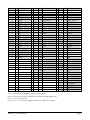
1
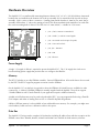
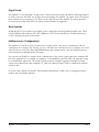
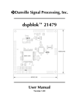
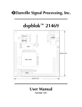
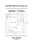
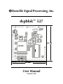
Danville Signal Processing, Inc.
dspblok™ 527
EEPROM
CLOCK
+
FLASH
RMII
+
60.00 [2.36]
ADSP-BF527
SDRAM
JTAG
60.00 [2.36]
User Manual
Version 1.20
Danville Signal Processing, Inc.
dspblok™ 527
User Manual
Copyright © 2009-2012 Danville Signal Processing, Inc. All rights reserved. Printed in the USA.
Under the copyright laws, this manual may not be reproduced in any form without prior written permission
from Danville Signal Processing, Inc.
Danville Signal Processing, Inc. strives to deliver the best product to our customers. As part of this goal, we
are constantly trying to improve our products. Danville Signal Processing, Inc., therefore, reserves the right to
make changes to product specification or documentation without prior notice. Updated operating manuals
and product specification sheets are available at our website for downloading.
This manual may contain errors, omissions or “typo’s”. Please send your comments, suggestions and
corrections to:
Danville Signal Processing, Inc.
38570 100th Avenue
Cannon Falls, MN 55009-5534
Trademark Notice
dspblok, dspFlash and dspBootloader are trademarks of Danville Signal Processing, Inc. VisualDSP++ and
Blackfin are trademarks of Analog Devices, Inc.
Contact Information
Danville Signal Processing, Inc.
38570 100th Avenue
Cannon Falls, MN 55009
E-mail:
Web Site:
[email protected]
http://www.danvillesignal.com
Voice:
507-263-5854
Fax:
877-230-5629
dspblok™ 527 User Manual
Page 1
Table of Contents
dspblok™ 527 ..........................................................................................................1
Table of Contents .....................................................................................................2
Overview..................................................................................................................3
dspblok™ 527........................................................................................................................................... 3
Intended Audience ...................................................................................................3
Getting Started..........................................................................................................4
Hardware Overview .................................................................................................5
Power Supply............................................................................................................................................ 5
Memory.................................................................................................................................................... 5
Data Bus ................................................................................................................................................... 5
Clocks....................................................................................................................................................... 6
USB .......................................................................................................................................................... 6
Ethernet .................................................................................................................................................... 6
Reset......................................................................................................................................................... 6
Signal Levels ............................................................................................................................................. 7
Boot Options ............................................................................................................................................ 7
Multiprocessor Configurations ................................................................................................................... 7
Connections .............................................................................................................8
Connector Recommendations & Notes ...................................................................10
Connector Specification .......................................................................................................................... 10
JH1 – JTAG (External ICE)........................................................................................................................ 10
JH2 – IO ................................................................................................................................................. 10
JH3 – Boot Mode and Reset.................................................................................................................... 10
JH4 – Power & Clock .............................................................................................................................. 10
JH5, JH7 – Data Bus ............................................................................................................................... 11
JH8 – USB .............................................................................................................................................. 11
JH9 – Ethernet ........................................................................................................................................ 11
Mechanical Dimensions..........................................................................................12
Schematic...............................................................................................................13
RoHS & WEEE Compliance.....................................................................................13
dspblok™ 527 User Manual
Page 2
Overview
Danville Signal's dspblok™ family of products delivers the power of digital signal processing in a small 60mm
x 60mm form factor. Connections are brought out to standard 2mm dual row headers. The dspblok reduces
development costs, risk and time.
Danville’s dspblok DSP function modules are often incorporated directly into larger custom embedded
systems. By taking advantage of pretested signal processing modules, pc board layouts become simpler and
projects are completed quickly and cost effectively.
You can also create small standalone embedded applications by combining a dspblok DSP function module
with other dspblok modules. Embedded dspblok systems are created by using a dspblok power supply, such
as our dspblok ps-usb or dspblok ps-uart and an I/O module, such as one of our dspblok ad96k family of
audio data converter boards. Each board is stacked via 2mm headers to create a low profile configuration
where space is at a premium.
The dspblok 527 has simultaneous support for both the USB and the Ethernet peripherals of the Blackfin
527. The high speed USB can be configured as a host, peripheral or as USB-On-The-Go. The Ethernet
peripheral includes an on-board LAN8700 RMII PHY. All you need to add is a connector with integrated
magnetics. Alternatively, you can interface to Power-over-Ethernet (POE) circuits.
dspblok™ 527
The dspblok™ 527 is a highly integrated DSP module that incorporates an Analog Devices’ Blackfin BF527
operating at 600 MHz with RMII Ethernet PHY, programmable clock, flash, EEProm and SDRAM memory.
An on-board switching power supply supports the core voltage requirements of the DSP so that only 3.3V is
required to power the dspblok. The Blackfin BF527 peripherals include USB 2.0, Ethernet, PPI, HOSTDP,
SPORTs(2), UARTs(2), TWI, SPI, RTC, NFC, JTAG and a 16 bit wide data bus. All of these peripherals are
available via 2mm headers on the dspblok.
Intended Audience
The dspblok 527 requires an understanding of the Analog Devices’ Blackfin BF527 and the associated tools
used for development. If the dspblok 527 is going to be integrated into a larger hardware design, then it is
also assumed that the user is familiar with basic hardware design. In most cases, systems integrators, DSP
programmers and software engineers can create DSP embedded systems using our embedded dspblok
systems (or dspstak family) without the need for additional hardware design and manufacturing.
If you do not have a background with these skills, you may want to check out our web site
(http://www.danvillesignal.com) as well as the Analog Devices web site for links to useful references. Danville
engineers are also available to discuss your application.
dspblok™ 527 User Manual
Page 3
Getting Started
The dspblok 527 includes the following items:
Hardware:
•
•
dspblok 527 Module
Mating 2mm female headers
Documents (CD):
•
•
This Manual
Schematics
Software (CD):
•
•
•
ADI Flash programmer driver (requires ADI ICE & VisualDSP++)
dspblok 527 configuration file (VisualDSP++ 5.0)
USB VDK software example
We recommend that you have the documents:
•
•
Analog Devices ADSP-BF527 Blackfin Processor Hardware Reference Manual
Analog Devices ADSP-BF53X/56X Blackfin Processor Programming Reference Manual
We recommend that you have the following tools:
•
•
•
•
Analog Devices VisualDSP++ 5.0 for Blackfin (available from Danville)
Danville dspFlash Blackfin & SHARC Programmer
Analog Devices HP USB ICE or USB ICE (available from Danville)
Danville DSP JTAG adapter
Our website (www.danvillesignal.com) has downloads and links to other tools and documents.
dspblok™ 527 User Manual
Page 4
Hardware Overview
The dspblok 527 is a small module measuring 60mm x 60mm (2.36” x 2.36”). JH2, JH4-JH8 are 2mm male
headers that are installed on the bottom side of the pc assembly. JH1 is mounted on the top side of the pc
assembly. JH8 is a series of three connectors. If mating 2mm female headers (4.3mm ht.) are used, the pc
assembly will be about ¼” above the mating pc board. This allows standard sized standoffs to be used with
the corner mounting holes if desired. The hole size is 2.3mm (0.090”) – suitable for 2-56 screws.
JH9
JH8
JH4
EEPROM
CLOCK
JH1 – JTAG (connects to external ICE)
•
JH2 – PORT F, G and PPI control signals
•
JH3 – Boot mode and reset pins (Top side)
•
JH4 – Power & Ext Clock
•
JH5, JH7 – Data Bus
•
JH8 –USB
•
JH9 - Ethernet
+
FLASH
•
RMII
+
60.00 [2.36]
JH2
ADSP-BF527
JH1
JH7
60.00 [2.36]
JH5
SDRAM
JH3
JTAG
Power Supply
A single 3.3V supply is all that is required to power the dspblok 527. The 3.3V supply also feeds an onboard switching power supply that provides the core voltage to the Blackfin.
Memory
The BF527 includes an on-chip SDRAM controller. External SDRAM allows 16 bit wide data to be accessed
by the DSP. The BF527 supports program execution from the SDRAM.
On the dspblok 527, no AMS pin is required to select the SDRAM. All 4 AMS lines are available for other
connections. A 16Mx16 (256Mbit) SDRAM is normally supplied with the dspblok. The pcb can support
512Mbit SDRAM as well. Consult Danville if your application requires additional memory.
A 4Mbit serial flash memory may be used to bootload the DSP. You can program the flash using a Danville
JTAG adapter and either an Analog Devices ICE or a Danville dspFlash Programmer.
64kbits of EEProm memory is also available as byte addressable user memory. For example, you might store
serial numbers, build versions or calibration values in this space.
Data Bus
The dspblok 527 brings out the complete 16-bit data bus including all address lines with the exception of the
SDRAM control lines. #AMS0, #AMS1, #AMS2 and #AMS3 are available for bank memory selection.
dspblok™ 527 User Manual
Page 5
Clocks
The dspblok 527 has an on-board programmable Cypress CY22393 clock generator. This clock generator
supplies 50 MHz for the Ethernet, 24MHz for the USB, 22.1184 or 24 MHz to the DSP and a programmable
clock for output. The clock generator can be reprogrammed through the TWI (I2C) interface, see the
CY22393 datasheet for programming procedures.
The DSP clock is selectable for either 24.000MHz or 22.1184MHz operation via the CLKSEL pin on JH8C.
The 24 MHz frequency allows the processor to operate at its maximum core clock of 600 MHz. Setting the
DSP clock to 22.1184 MHz allows the UART to operate at precise standard baud rates.
USB
The dspblok 527 has full support for the Blackfin’s built-in USB On-The-Go (OTG) controller. This allows the
DSP to operate as either a USB Host or a USB Slave device. Host operation makes it possible to interface
directly to peripheral devices such as digital cameras, USB flash drives or USB keyboards.
It is important to note that the USB signal connections are fast and should be treated as such. The USB lines
should be kept as short as possible to a mating connector. If they need to be longer, they should be treated
as controlled impedance lines.
Ethernet
The dspblok 527 has an on-board LAN8700 ethernet RMII PHY. This means that all that is necessary for
Ethernet communication is a connector with integrated magnetics, which could be an RJ-45 connector to use
standard Ethernet cables or could be a more custom connection type. The EEProm includes a predefined
MAC address.
Analog Devices supplies a royalty free TCP-IP stack with VisualDSP called the lwip stack. With this portion of
the Ethernet application already written the difficulty of the Ethernet development process is greatly reduced.
ADI also supplies reference designs of an HTTP server, INETD server, which allows for Telnet
communication, and others.
Reset
The dspblok 527 automatically resets when the 3.3V power supply is stable. #RESET is active low and open
drain. This means that an external device(s) may also reset the dspblok by pulling the reset line low. External
devices should not drive #RESET high since this can cause contention with the on-board reset circuit. The
external reset circuit is connected in a wired-OR configuration using an active low – open drain
configuration. A 74LVC125 or an open collector/drain transistor circuit are possibilities. You do not need an
additional pull up resistor.
The Reset line can also be accessed on JH3. This would allow you to reset the processor by placing a
shorting jumper across the 2 pins closest to the edge of the board (pins 9 and 10).
dspblok™ 527 User Manual
Page 6
Signal Levels
The dspblok 527 uses standard 3.3V logic levels. These levels have become the defacto operating standard
for many years now. DO NOT use 5V logic when interfacing to the dspblok. The inputs are not 5V tolerant.
Most external devices requiring 5V TTL levels can be safely driven by the dspblok. If you have questions
concerning interfacing external devices, please contact Danville for suggestions.
Boot Options
All Blackfin BF527 boot options are available via the configuration and programming header (JH3). These
include EPROM (flash memory), SPI, OTP, SDRAM or JTAG. The boot mode pins are pulled passively to
create a default boot mode of SPI Master.
Multiprocessor Configurations
The dspblok 527 may be used as a coprocessor in a larger system. One way to communicate with an
external host is to configure the SPI port as a slave. This will mean it will be necessary to halt the uses of the
other SPI devices such as the flash and EEPROM during the communication, and care should be taken to
avoid contention in multiple master SPI system.
You can also use SPORTs for interprocessor communication. This can be a good approach in multiple DSP
processor applications. For example, you might use several dspbloks to provide front end signal processing
for a multichannel application. The results could be routed to a dspblok+fpga that manages the whole
system and communicates with a dspblok 527, which uses Ethernet and/or USB to communicate with the
outside world.
Of course, other options are possible. These include USB, Ethernet, UARTs, I2C or creating an external
mailbox style I/O with the data bus.
dspblok™ 527 User Manual
Page 7
Connections
Pin
JH1
Note 1
Description
JTAG
1
2
3
4
5
6
7
8
9
10
11
12
13
14
15
16
EMUSEL
EMU
Key (No Pin)
GND
Vd+3.3 Mon
TMS
GND
TCK
GND
#TRST
GND
TDI
GND
TDO
Vd+3.3
Vd+3.3
dspblok™ 527 User Manual
Pin
JH2
Note 2
Description
DAI, DPI, IO
1
2
3
4
5
6
7
8
9
10
11
12
13
14
15
16
17
18
19
20
21
22
23
24
25
26
27
28
29
30
31
32
33
34
35
36
37
38
39
40
GND
SPISS
PG12
PG13
PG5
PH15
PG6
SDA
SCL
PG7
PG8
PPIFS
PPICLK
MOSI_EXT
SCK_EXT
MISO
#RESET
HWAIT
PH11
PG9
PG10
PG11
PF8
PF9
PF10
PF11
PF12
PF13
PF14
PF15
PF9
PF0
PF1
PF4
PF2
PF5
PF6
PF7
GND
GND
Pin
JH3
JTAG - AUX
1
2
3
4
5
6
7
8
9
10
JH4
Note 4
Note 3
Note 3
Description
GND
BMODE0
GND
BMODE1
VD+3.3
BMODE2
VD+3.3
BMODE3
GND
RESET
Power
1
2
3
4
5
6
7
8
9
10
GND
Ext Clk
ExtWake
DSP ClkOut
Vd+3.3
Vd+3.3
Reserved
Reserved
Vbatt
GND
Page 8
Pin
JH5
Description
Data Bus
1
2
3
4
5
6
7
8
9
10
11
12
13
14
15
16
17
18
19
20
D15
D14
D13
D12
D11
D10
D9
D8
D7
D6
D5
D4
D3
D2
D1
D0
AOE
AWE
ARDY
ARE
Pin
JH7
Note 3
Note 3
Note 3
Note 3
Note 3
Note 3
Description
Data Bus
1
2
3
4
5
6
7
8
9
10
11
12
13
14
15
16
17
18
19
20
21
22
23
24
25
26
27
28
29
30
AMS3
Reserved
Reserved
Reserved
Reserved
Reserved
Reserved
A19
A18
A17
A16
A15
A14
A13
A12
A11
A10
A9
A8
A7
A6
A5
A4
A3
A2
A1
A0
AMS0
AMS1
AMS2
Pin
JH8
Description
USB
1
2
3
4
5
6
7
8
9
10
11
12
13
14
15
16
JH9
GND
PH11
USB_VBUS
USB_ID
GND
GND
USB_P
USB_N
GND
GND
CLK SEL
GND
PH15
GND
PH14
GND
Ethernet
1
2
3
4
5
6
7
8
9
10
11
12
13
14
15
16
RDRD+
TCT
TDTD+
GND
LINK LED#
FD LED#
GND
GND
Vd+3.3
Note 1: Mating Plug is plugged to prevent misalignment.
Note 2: DPI4 also functions as #SPIDS in SPI slave booting applications.
Note 3: Leave Unconnected.
Note 4: Vd+1.3 is for power supply monitor only (DSP Core supply).
dspblok™ 527 User Manual
Page 9
Connector Recommendations & Notes
Connector Specification
All dspblok connectors are gold plated 2mm dual row headers. Male connectors are either soldered on the
dspblok pc assembly or supplied for optional assembly by the customer. Mating female connectors are
included for your target pc board. The plastic base of each male connector is 2mm. The height of the female
headers is 4.3mm. This means that the inserted combined height of the two connectors is 6.3mm or
approximately ¼ inch. Standard standoffs may be used to secure the dspblok to the target pc board.
Mounting holes are 2.3mm (0.090 inch) dia. to accommodate a 2-56 screws or standoffs.
JH1 – JTAG (External ICE)
This connector is mounted on the top side of the dspblok. A 2mm right angle header is used instead of the
larger ADI JTAG header. The connections on the JTAG header correspond with the connections on an ADI
JTAG header. In addition, Vd+3.3 is also available. This addition allows an active buffer circuit to be added
for JTAG chaining applications. Danville has an ADI JTAG adapter available (P/N A.08153).
JH2 – IO
This connector is mounted on the bottom side of the dspblok. The I/O lines are all uncommitted by the
dspblok. PORT F and most of PORT G are available on this connector and can be used as either GPIO or
their built in alternate functions.
JH3 – Boot Mode and Reset
This connector can be mounted on the top or bottom side of the dspblok. It is used to allow a mating board
or the user to change the boot mode or issue a hardware reset. There are pull-ups and pull-downs to
configure the default boot mode to SPI boot mode (0011). Shorting the adjacent odd-even pins on the
connector will invert the bit. For example a jumper on Boot Mode 3 (pins 1,2) will result in boot mode
1011. A second example of this if a jumper is placed on Boot Mode 1 (pins 5,6) will result in boot mode
0001.
By default this connector is mounted on the top side of the dspblok 527. If you would like it to be mounted
on the bottom side of the dspblok 527 please contact Danville Signal and be sure to specify this when
ordering.
JH4 – Power & Clock
This connector is mounted on the bottom side of the dspblok. This is the main power feed to the dspblok.
An external battery supply may be connected for RTC (real time clock) operation.
dspblok™ 527 User Manual
Page 10
JH5, JH7 – Data Bus
The data bus is split to two separate connectors, JH5 is the 16 bit data bus and JH7 is the address bus. The
address bus is also organized so that the AMS lines and the lower address lines are grouped together. This
allows a smaller receptacle to be used when the whole address space is not required. JH6 is omitted for
dspblok family compatibility.
JH8 – USB
JH8 is the USB connector and comes directly from the USB pins on the DSP. To ensure optimal USB
performance the data lines of the USB should be laid out with care as well. The USB controller is capable of
USB On The Go, which means the USB can act not only as a peripheral but as a host as well. This allows for
interfacing directly with other peripherals such as digital cameras, flash drives, and most other USB devices.
The Clk Sel will default to 24 MHz which is needed for USB operation, and if jumpered will be 22.118 MHz.
This is useful for UART communications since it allows standard bauds to be supported..
JH9 – Ethernet
JH9 is the Ethernet connector. These connections are typically connected to an integrated magnetics RJ-45
connector. The RDA-125BAG1A from Saelig Company is a possible choice.
dspblok™ 527 User Manual
Page 11
Mechanical Dimensions
6.00 [0.24]
C9
+
RN12
44.00[1.73]
D1
CD29
U2
RN7
RN8 RN20
R2
U1
C2
L1
U5
U3
Top Side
CD33
C7
C8
Y2
U8
R17
RN22 R18
C24
U9
C25
Q1
U7
U6
60.00[2.36]
C31
C32 D2
Y1
+
CD36
U4 RN3 RN1 RN4 RN2
24.00 [0.94]
RN6
9.00 [0.35]
JH1
6.00 [0.24]
26.00 [1.02]
57.00 [2.24]
60.00 [2.36]
Holes 2.3 [0.090] (4 places)
JH4
JH8
JH9
Bottom Side
55.00[2.17]
JH2
JH5
JH3
JH7
55.00 [2.17]
Mounting holes are equidistant from the center of the dspblok. These holes are 0.090 in diameter, suitable
for 2-56 screws. When 4.3mm height mating female connectors are used, the board will be 6.3mm (0.25 in)
above the target board, therefore 0.250 standoffs may be used.
Component height above the board is 6mm (0.236 in). The board is .062 in thick.
dspblok™ 527 User Manual
Page 12
Schematic
The Distribution CD includes schematic diagrams of the dspblok 527.
RoHS & WEEE Compliance
The European Union approved a directive on the restriction of the use of certain hazardous substances in
electrical and electronic equipment. This directive is commonly known as RoHS, EU Directive 2002/95/EC.
This directive severely limits the amount of lead and 5 other substances that can be in contained in
nonexempt products. The directive became European law in February 2003 and took effect July 1, 2006.
It is likely that other countries outside the European Union and some states in the United States may adopt
similar legislation.
There are a number of important exemptions that affect many of our customers. The most important of these
is Category 9, Control and Monitoring Instruments. You may wish to review your situation to see if this
exemption applies to you. Military, medical and some other products are also exempt. We suggest that you
make an appropriate assessment concerning your products.
The dspblok 527 is RoHS compliant.
The dspblok 527 is a subcomponent of a larger system; therefore it is not subject to the WEEE directive EU
Directive 2002/96/EC.
dspblok™ 527 User Manual
Page 13