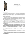
1
Agilent 75000 SERIES C
Agilent E1490C
C-Size VXIbus Register-Based
Breadboard Module
User’s Manual
*E1490-90004*
Manual Part Number E1490-90004
Printed in Malaysia E0806
Contents
Agilent E1490C User’s Manual
Warranty . . . .
WARNINGS . .
Safety Symbols
User Notes . . .
.
.
.
.
.
.
.
.
.
.
.
.
.
.
.
.
.
.
.
.
.
.
.
.
.
.
.
.
.
.
.
.
.
.
.
.
.
.
.
.
.
.
.
.
.
.
.
.
.
.
.
.
.
.
.
.
.
.
.
.
.
.
.
.
.
.
.
.
.
.
.
.
.
.
.
.
.
.
.
.
.
.
.
.
.
.
.
.
.
.
.
.
.
.
.
.
.
.
.
.
.
.
.
.
.
.
.
.
.
.
.
.
.
.
.
.
.
.
.
.
.
.
.
.
.
.
.
.
.
.
.
.
.
.
.
.
.
.
.
.
.
.
.
.
.
.
.
.
.
.
.
.
3
4
4
5
Chapter 1. Introduction . . . . . . . . . . . . . . . . . . . . . . . . . . . . . . . . . . . . . 7
Manual Contents . . . . . . . . . . . .
Specification Compliance/Warranty .
Agilent E1490C Description . . . . .
Breadboard Module Features . . . .
Backplane Interface Features . . .
Agilent E1490C Hardware Features
.
.
.
.
.
.
.
.
.
.
.
.
.
.
.
.
.
.
.
.
.
.
.
.
.
.
.
.
.
.
.
.
.
.
.
.
.
.
.
.
.
.
.
.
.
.
.
.
.
.
.
.
.
.
.
.
.
.
.
.
.
.
.
.
.
.
.
.
.
.
.
.
.
.
.
.
.
.
.
.
.
.
.
.
.
.
.
.
.
.
.
.
.
.
.
.
.
.
.
.
.
.
.
.
.
.
.
.
.
.
.
.
.
.
.
.
.
.
.
.
.
.
.
.
.
.
.
.
.
.
.
.
.
.
.
.
.
.
.
.
.
.
.
.
.
.
.
.
.
.
.
.
.
.
.
.
7
7
8
8
8
11
Chapter 2. Configuring the Agilent E1490C . . . . . . . . . . . . . . . . . . . . . . . . . 13
Handling Precautions . . . . . . . . . . . . . . . . .
Reducing Risk of Static Discharge Damage . . . .
Hardware Description . . . . . . . . . . . . . . . . .
Backplane Connections . . . . . . . . . . . . . .
Backplane Connector Pins . . . . . . . . . . . . .
Terminal Module Connections . . . . . . . . . . .
Module Dimensions . . . . . . . . . . . . . . . . . .
Metal Standoffs . . . . . . . . . . . . . . . . . . .
Cooling Requirements . . . . . . . . . . . . . . . . .
Setting the Logical Address Switch . . . . . . . . . .
Setting the Interrupt Priority . . . . . . . . . . . . . .
Installing the Breadboard in a Mainframe . . . . . . .
Terminal Modules . . . . . . . . . . . . . . . . . . .
Screw-type Terminal Module . . . . . . . . . . .
Wiring Guidelines . . . . . . . . . . . . . . . .
Terminal Module Option A3E . . . . . . . . . . .
Crimp-and-Insert Terminal Module Accessories .
Single-Conductor and Contact . . . . . . . . . .
Shielded-Twisted-Pair and Contacts . . . . . . .
Jumper Wire and Contacts . . . . . . . . . . . .
Crimp-and-Insert Contacts . . . . . . . . . . . .
Crimp-and-Insert Tools . . . . . . . . . . . . . .
Extra Crimp-and-Insert Connectors . . . . . . .
Wiring a Terminal Module . . . . . . . . . . . . . .
Attaching a Terminal Module to the Breadboard . . .
Backplane Interface Circuitry . . . . . . . . . . . . .
Address Lines and Register Decoding . . . . . . .
Data Bus Drivers . . . . . . . . . . . . . . . . . .
Status Register . . . . . . . . . . . . . . . . . . .
ID Register . . . . . . . . . . . . . . . . . . . . .
.
.
.
.
.
.
.
.
.
.
.
.
.
.
.
.
.
.
.
.
.
.
.
.
.
.
.
.
.
.
.
.
.
.
.
.
.
.
.
.
.
.
.
.
.
.
.
.
.
.
.
.
.
.
.
.
.
.
.
.
.
.
.
.
.
.
.
.
.
.
.
.
.
.
.
.
.
.
.
.
.
.
.
.
.
.
.
.
.
.
.
.
.
.
.
.
.
.
.
.
.
.
.
.
.
.
.
.
.
.
.
.
.
.
.
.
.
.
.
.
.
.
.
.
.
.
.
.
.
.
.
.
.
.
.
.
.
.
.
.
.
.
.
.
.
.
.
.
.
.
.
.
.
.
.
.
.
.
.
.
.
.
.
.
.
.
.
.
.
.
.
.
.
.
.
.
.
.
.
.
.
.
.
.
.
.
.
.
.
.
.
.
.
.
.
.
.
.
.
.
.
.
.
.
.
.
.
.
.
.
.
.
.
.
.
.
.
.
.
.
.
.
.
.
.
.
.
.
.
.
.
.
.
.
.
.
.
.
.
.
.
.
.
.
.
.
.
.
.
.
.
.
.
.
.
.
.
.
.
.
.
.
.
.
.
.
.
.
.
.
.
.
.
.
.
.
.
.
.
.
.
.
.
.
.
.
.
.
.
.
.
.
.
.
.
.
.
.
.
.
.
.
.
.
.
.
.
.
.
.
.
.
.
.
.
.
.
.
.
.
.
.
.
.
.
.
.
.
.
.
.
.
.
.
.
.
.
.
.
.
.
.
.
.
.
.
.
.
.
.
.
.
.
.
.
.
.
.
.
.
.
.
.
.
.
.
.
.
.
.
.
.
.
.
.
.
.
.
.
.
.
.
.
.
.
.
.
.
.
.
.
.
.
.
.
.
.
.
.
.
.
.
.
.
.
.
.
.
.
.
.
.
.
.
.
.
.
.
.
.
.
.
.
.
.
.
.
.
.
.
.
.
.
.
.
.
.
.
.
.
.
.
.
.
.
.
.
.
.
.
.
.
.
.
.
.
.
.
.
.
.
.
.
.
.
.
.
.
.
.
.
.
.
.
.
.
.
.
.
.
.
.
.
.
.
.
.
.
.
.
.
.
.
.
.
.
.
.
.
.
.
.
.
.
.
.
.
.
.
.
.
.
.
.
.
.
.
.
.
.
.
.
.
.
.
.
.
.
.
.
.
.
.
.
.
.
.
.
.
.
13
14
14
16
16
17
17
20
22
23
24
25
26
26
26
27
27
27
27
28
28
28
28
29
31
32
32
35
36
37
Agilent E1490C User’s Manual Contents
1
Chapter 2. Configuring the Agilent E1490C (continued)
Device Type Register . . . . .
Control Register . . . . . . . .
DTACK, Interrupt, and Control
DTACK . . . . . . . . . . . .
Interrupt . . . . . . . . . . . .
Control . . . . . . . . . . . .
ECL Trigger Logic . . . . . . .
User Access Points . . . . . . .
Power Supplies . . . . . . . . .
Custom Circuitry . . . . . . . . .
Relay Selection . . . . . . . . .
Notifying the Controller . . . .
.
.
.
.
.
.
.
.
.
.
.
.
.
.
.
.
.
.
.
.
.
.
.
.
.
.
.
.
.
.
.
.
.
.
.
.
.
.
.
.
.
.
.
.
.
.
.
.
.
.
.
.
.
.
.
.
.
.
.
.
.
.
.
.
.
.
.
.
.
.
.
.
.
.
.
.
.
.
.
.
.
.
.
.
.
.
.
.
.
.
.
.
.
.
.
.
.
.
.
.
.
.
.
.
.
.
.
.
.
.
.
.
.
.
.
.
.
.
.
.
.
.
.
.
.
.
.
.
.
.
.
.
.
.
.
.
.
.
.
.
.
.
.
.
.
.
.
.
.
.
.
.
.
.
.
.
.
.
.
.
.
.
.
.
.
.
.
.
.
.
.
.
.
.
.
.
.
.
.
.
.
.
.
.
.
.
.
.
.
.
.
.
.
.
.
.
.
.
.
.
.
.
.
.
.
.
.
.
.
.
.
.
.
.
.
.
.
.
.
.
.
.
.
.
.
.
.
.
.
.
.
.
.
.
.
.
.
.
.
.
.
.
.
.
.
.
.
.
.
.
.
.
.
.
.
.
.
.
.
.
.
.
.
.
.
.
.
.
.
.
.
.
.
.
.
.
.
.
.
.
.
.
.
.
.
.
.
.
.
.
.
.
.
.
.
.
.
.
.
.
.
.
.
.
.
.
.
.
.
.
.
.
.
.
.
.
.
.
.
.
.
.
.
.
.
.
.
.
.
.
.
.
.
.
.
.
38
40
41
41
43
44
45
46
47
47
47
48
Chapter 3. Using the Agilent E1490C . . . . . . . . . . . . . . . . . . . . . . . . . . . . . 51
Reading Data From Registers . . . . . . .
Status Register Bit Definitions . . . . .
Reading the Status Register . . . . . .
Reading ID and Device Type Registers
Writing Data to the Control Register . . .
Control Register Bit Definitions . . . .
Writing to the Control Register . . . .
Using Interrupts . . . . . . . . . . . . . .
Configuring for Interrupts . . . . . . .
Generating Interrupt Requests . . . . .
Resetting the Module . . . . . . . . . . .
Hardware Reset . . . . . . . . . . . . .
Software Reset . . . . . . . . . . . . .
Detecting Errors . . . . . . . . . . . . . .
Using Other Power Supplies . . . . . . . .
Example Programs . . . . . . . . . . . . .
Reading the Registers . . . . . . . . .
Register Definitions . . . . . . . . . .
Reading the ID Register . . . . . . .
Reading the Device Type Register . .
Writing to the Control Register . . . .
Reading/Writing to Custom Registers .
.
.
.
.
.
.
.
.
.
.
.
.
.
.
.
.
.
.
.
.
.
.
.
.
.
.
.
.
.
.
.
.
.
.
.
.
.
.
.
.
.
.
.
.
.
.
.
.
.
.
.
.
.
.
.
.
.
.
.
.
.
.
.
.
.
.
.
.
.
.
.
.
.
.
.
.
.
.
.
.
.
.
.
.
.
.
.
.
.
.
.
.
.
.
.
.
.
.
.
.
.
.
.
.
.
.
.
.
.
.
.
.
.
.
.
.
.
.
.
.
.
.
.
.
.
.
.
.
.
.
.
.
.
.
.
.
.
.
.
.
.
.
.
.
.
.
.
.
.
.
.
.
.
.
.
.
.
.
.
.
.
.
.
.
.
.
.
.
.
.
.
.
.
.
.
.
.
.
.
.
.
.
.
.
.
.
.
.
.
.
.
.
.
.
.
.
.
.
.
.
.
.
.
.
.
.
.
.
.
.
.
.
.
.
.
.
.
.
.
.
.
.
.
.
.
.
.
.
.
.
.
.
.
.
.
.
.
.
.
.
.
.
.
.
.
.
.
.
.
.
.
.
.
.
.
.
.
.
.
.
.
.
.
.
.
.
.
.
.
.
.
.
.
.
.
.
.
.
.
.
.
.
.
.
.
.
.
.
.
.
.
.
.
.
.
.
.
.
.
.
.
.
.
.
.
.
.
.
.
.
.
.
.
.
.
.
.
.
.
.
.
.
.
.
.
.
.
.
.
.
.
.
.
.
.
.
.
.
.
.
.
.
.
.
.
.
.
.
.
.
.
.
.
.
.
.
.
.
.
.
.
.
.
.
.
.
.
.
.
.
.
.
.
.
.
.
.
.
.
.
.
.
.
.
.
.
.
.
.
.
.
.
.
.
.
.
.
.
.
.
.
.
.
.
.
.
.
.
.
.
.
.
.
.
.
.
.
.
.
.
.
.
.
.
.
.
.
.
.
.
.
.
.
.
.
.
.
.
.
.
.
.
.
.
.
.
.
.
.
.
.
.
.
.
.
.
.
.
.
.
.
.
.
.
.
.
.
.
.
.
.
.
.
.
.
.
.
.
.
.
.
.
.
.
.
.
.
.
.
.
.
.
.
.
.
.
.
.
.
.
.
.
.
.
.
.
.
.
.
.
.
.
.
.
.
.
.
.
.
.
.
.
.
.
.
.
.
.
51
51
52
53
54
54
55
57
57
57
59
59
59
59
60
61
61
61
61
61
61
62
Appendix A. Agilent E1490C Breadboard Specifications . . . . . . . . . . . . . . . . . . 63
Specifications Table . . . . . . . . . . . . . . . . . . . . . . . . . . . . . . . . . . . . 63
Appendix B. Agilent E1490C Parts List, Component Locator, and Schematics . . . . . . 65
Backplane Interface Component Locator . . . . . . . . . . . . . . . . . . . . . . 66
Backplane Interface Schematic . . . . . . . . . . . . . . . . . . . . . . . . . . . . 66
Index . . . . . . . . . . . . . . . . . . . . . . . . . . . . . . . . . . . . . . . . . . . . . . . . 73
2
Agilent E1490C User’s Manual Contents
Certification
Agilent Technologies certifies that this product met its published specifications at the time of shipment from the factory. Agilent
Technologies further certifies that its calibration measurements are traceable to the United States National Institute of Standards and
Technology (formerly National Bureau of Standards), to the extent allowed by that organization’s calibration facility, and to the calibration
facilities of other International Standards Organization members.
Warranty
This Agilent Technologies product is warranted against defects in materials and workmanship for a period of one (1) year from date of
shipment. Duration and conditions of warranty for this product may be superseded when the product is integrated into (becomes a part
of) other Agilent products. During the warranty period, Agilent Technologies will, at its option, either repair or replace products which
prove to be defective.
For warranty service or repair, this product must be returned to a service facility designated by Agilent Technologies. Buyer shall prepay
shipping charges to Agilent and Agilent shall pay shipping charges to return the product to Buyer. However, Buyer shall pay all shipping
charges, duties, and taxes for products returned to Agilent from another country.
Agilent warrants that its software and firmware designated by Agilent for use with a product will execute its programming instructions
when properly installed on that product. Agilent does not warrant that the operation of the product, or software, or firmware will be
uninterrupted or error free.
Limitation Of Warranty
The foregoing warranty shall not apply to defects resulting from improper or inadequate maintenance by Buyer, Buyer-supplied products
or interfacing, unauthorized modification or misuse, operation outside of the environmental specifications for the product, or improper site
preparation or maintenance.
The design and implementation of any circuit on this product is the sole responsibility of the Buyer. Agilent does not warrant the Buyer’s
circuitry or malfunctions of Agilent products that result from the Buyer’s circuitry. In addition, Agilent does not warrant any damage that
occurs as a result of the Buyer’s circuit or any defects that result from Buyer-supplied products.
NO OTHER WARRANTY IS EXPRESSED OR IMPLIED. Agilent SPECIFICALLY DISCLAIMS THE IMPLIED WARRANTIES
OF MERCHANTABILITY AND FITNESS FOR A PARTICULAR PURPOSE.
Exclusive Remedies
THE REMEDIES PROVIDED HEREIN ARE BUYER’S SOLE AND EXCLUSIVE REMEDIES. Agilent SHALL NOT BE LIABLE
FOR ANY DIRECT, INDIRECT, SPECIAL, INCIDENTAL, OR CONSEQUENTIAL DAMAGES, WHETHER BASED ON CONTRACT, TORT, OR ANY OTHER LEGAL THEORY.
Notice
The information contained in this document is subject to change without notice. Agilent Technologies MAKES NO WARRANTY OF
ANY KIND WITH REGARD TO THIS MATERIAL, INCLUDING, BUT NOT LIMITED TO, THE IMPLIED WARRANTIES OF
MERCHANTABILITY AND FITNESS FOR A PARTICULAR PURPOSE. Agilent shall not be liable for errors contained herein or for
incidental or consequential damages in connection with the furnishing, performance or use of this material. This document contains
proprietary information which is protected by copyright. All rights are reserved. No part of this document may be photocopied, reproduced,
or translated to another language without the prior written consent of Agilent Technologies, Inc. Agilent assumes no responsibility for the
use or reliability of its software on equipment that is not furnished by Agilent.
U.S. Government Restricted Rights
The Software and Documentation have been developed entirely at private expense. They are delivered and licensed as "commercial
computer software" as defined in DFARS 252.227- 7013 (Oct 1988), DFARS 252.211-7015 (May 1991) or DFARS 252.227-7014 (Jun
1995), as a "commercial item" as defined in FAR 2.101(a), or as "Restricted computer software" as defined in FAR 52.227-19 (Jun 1987)(or
any equivalent agency regulation or contract clause), whichever is applicable. You have only those rights provided for such Software and
Documentation by the applicable FAR or DFARS clause or the Agilent standard software agreement for the product involved.
Agilent E1490C C-Sized VXIbus Register-Based Breadboard Module User’s Manual
Edition 3 Rev 2
Copyright © 1996-2006 Agilent Technologies, Inc. All Rights Reserved.
Agilent E1490C C-Sized VXIbus Register-Based Breadboard Module User’s Manual
3
Printing History
The Printing History shown below lists all Editions and Updates of this manual and the printing date(s). The first printing of the manual
is Edition 1. The Edition number increments by 1 whenever the manual is revised. Updates, which are issued between Editions, contain
replacement pages to correct the current Edition of the manual. Updates are numbered sequentially starting with Update 1. When a new
Edition is created, it contains all the Update information for the previous Edition. Each new Edition or Update also includes a revised copy
of this printing history page. Many product updates or revisions do not require manual changes and, conversely, manual corrections may
be done without accompanying product changes. Therefore, do not expect a one-to-one correspondence between product updates and
manual updates.
Edition 1 . . . . . . . . . . . . . . . . . . . . . . . . . . . . . . . . . . . . . . . . . . . December 1990
Edition 2 . . . . . . . . . . . . . . . . . . . . . . . . . . . . . . . . . . . . . . . . . . . . . . . . May 1992
Edition 3 (Part Number E1490-90004). . . . . . . . . . . . . . . . . . . . . . . March 1996
Edition 3 Rev 2 (Part Number E1490-90004) . . . . . . . . . . . . . . . . . August 2006
Safety Symbols
Instruction manual symbol affixed to product.
Indicates that the user must refer to the manual for specific WARNING or CAUTION
information to avoid personal injury or damage to the product.
Alternating current (AC).
Direct current (DC).
Indicates hazardous voltages.
Indicates the field wiring terminal that must
be connected to earth ground before operating
the equipment—protects against electrical
shock in case of fault.
or
Frame or chassis ground terminal—typically
connects to the equipment’s metal frame.
WARNING
CAUTION
Calls attention to a procedure, practice, or condition that could cause bodily injury or death.
Calls attention to a procedure, practice, or condition that could possibly cause damage to
equipment or permanent loss of data.
WARNINGS
The following general safety precautions must be observed during all phases of operation, service, and repair of this product.
Failure to comply with these precautions or with specific warnings elsewhere in this manual violates safety standards of design,
manufacture, and intended use of the product. Agilent Technologies assumes no liability for the customer’s failure to comply with
these requirements.
Ground the equipment: For Safety Class 1 equipment (equipment having a protective earth terminal), an uninterruptible safety earth
ground must be provided from the mains power source to the product input wiring terminals or supplied power cable.
DO NOT operate the product in an explosive atmosphere or in the presence of flammable gases or fumes.
For continued protection against fire, replace the line fuse(s) only with fuse(s) of the same voltage and current rating and type.
DO NOT use repaired fuses or short-circuited fuse holders.
Keep away from live circuits: Operating personnel must not remove equipment covers or shields. Procedures involving the removal of
covers or shields are for use by service-trained personnel only. Under certain conditions, dangerous voltages may exist even with the
equipment switched off. To avoid dangerous electrical shock, DO NOT perform procedures involving cover or shield removal unless you
are qualified to do so.
DO NOT operate damaged equipment: Whenever it is possible that the safety protection features built into this product have been
impaired, either through physical damage, excessive moisture, or any other reason, REMOVE POWER and do not use the product until
safe operation can be verified by service-trained personnel. If necessary, return the product to an Agilent Technologies Sales and Service
Office for service and repair to ensure that safety features are maintained.
DO NOT service or adjust alone: Do not attempt internal service or adjustment unless another person, capable of rendering first aid and
resuscitation, is present.
DO NOT substitute parts or modify equipment: Because of the danger of introducing additional hazards, do not install substitute parts
or perform any unauthorized modification to the product. Return the product to an Agilent Technologies Sales and Service Office for
service and repair to ensure that safety features are maintained.
4
Agilent E1490C C-Sized VXIbus Register-Based Breadboard Module User’s Manual
Notes
Agilent E1490C C-Sized VXIbus Register-Based Breadboard Module User’s Manual
5
Notes
6
Agilent E1490C C-Sized VXIbus Register-Based Breadboard Module User’s Manual
Chapter 1
Introduction
Manual Contents
This manual has three chapters and two appendixes:
• Chapter 1 - Introduction summarizes manual contents, warranty
status, specification compliance, and includes a description of the
breadboard module.
• Chapter 2 - Configuring the Agilent E1490C describes module
hardware and dimensions, explains how to install the breadboard and
terminal module, terminal module options, and discusses operation
of the backplane interface circuits on the module. It also provides a
typical application example showing user circuits connected to the
backplane interface circuits.
• Chapter 3 - Using the Agilent E1490C shows how to use the
module in a VXIbus system.
• Appendix A - Agilent E1490C Breadboard Specifications lists the
hardware specifications for the Agilent E1490C module.
• Appendix B - Parts List, Component Locator, and Schematics
provides Agilent part numbers and descriptions of all parts supplied
by Agilent Technologies. A complete component locator and
schematic of the Agilent E1490C digital backplane interface is
included.
Specification Compliance/Warranty
The Agilent E1490C Breadboard Module is designed in full compliance
with the VXIbus System Specification (Revision 1.4).
WARNING
To prevent shock, use only wire rated for the highest input voltage
and disconnect all field power before removing terminal block
cover or assembly. Do not exceed 125 VACrms or 150 VDC on the
terminal module connector.
The Agilent E1490C warranty is different than the standard Agilent
Technologies warranty statement, located at the front of this manual. While
Agilent Technologies is responsible for defects in materials and workmanship
of the blank printed circuit board and supplied hardware, Agilent is not
responsible for the performance of your custom-designed circuitry. In addition,
Agilent Technologies is not responsible for damage to or improper operation of
your VXI mainframe or other plug-in modules caused by the Agilent E1490C
Breadboard Module.
Chapter 1
Introduction
7
Agilent E1490C Description
The Agilent E1490C Breadboard Module is a C-size register-based device
that provides a convenient interface to a VXI mainframe backplane. It
allows you to construct your own custom hardware for use with the
mainframe.
Breadboard Module
Features
The module provides VXI A16/D16 register-based backplane interface
circuitry and metal shields to enclose the printed circuit board. Your VXI
mainframe can communicate with this module configured as an A16/D16
device. The breadboard module interface circuitry is implemented and
accessible according to the requirements outlined in the VXIbus System
Specification.
Users can still provide custom extensions to expand module addressing
capability to A24 or A32 by adding appropriate circuitry according to the
VMEbus and VXIbus System Specification.
Backplane Interface
Features
Note
An overview of the Agilent E1490C interface features follows. See Figure
1-1.
For hardware operation, a mnemonic suffixed with an asterisk (such as
WRITE*) indicates inverse logic (0 or low = true; 1 or high = false).
A high state (1) is defined as a positive voltage (usually +5 V) and a low
state (0) is defined as zero V (ground) at the specified signal point.
The Agilent E1490C interface features are:
• Address Lines and Register Decoding. The module implements
15 address lines (A1 - A15) allowing:
1. decoding one of 255 switch-selectable logical device addresses in the
upper fourth of the A16 VME address space, and
2. selecting one of the breadboard configuration registers for read/write
operations. The module decodes the address modifier lines
AM0 - AM5 and acts on codes 2916 and 2D16 only.
See page 32 for information about address lines and register decoding.
• Data Lines. Data lines D0 - D15 are available for use on the
breadboard module. These 16 lines are buffered by data bus drivers
and used for writing to, and reading from, the configuration registers
(Status, ID, Device Type, and Control) via an internal data bus
(DB0 - DB15). See page 35 for information about data bus drivers
and data lines.
8
Introduction
Chapter 1
Figure 1-1. Digital Backplane Interface Block Diagram
Chapter 1
Introduction
9
• Status Register. Reading this 16-bit register provides information
about the status of the breadboard module. Implemented signals are
"A24/A32 Active", "MODID*", "Extended*" and "Passed". There
are also provisions for implementing device-dependent status bits.
See page 36 for information about the Status Register.
• ID Register. Reading this 16-bit register identifies the manufacturer
identification number, the device class, and the addressing mode of
the breadboard. By using the DIP switches, the user selects
hardwired configurations for these items. See page 37 for
information about the ID Register.
• Device Type Register. Reading this 16-bit register identifies the
unique card model as defined by the device manufacturer. It also
indicates the amount of memory available on the card in bytes (for
A24 and A32 devices only). By using the DIP switches, the user
selects hardwired configurations for these items. See page 38 for
information about the Device Type Register.
• Control Register. Writing to this 16-bit register causes specific
actions to be executed by the device. "Reset" and "System Fail
Inhibit" are implemented. Other device-dependent control bits may
be implemented by using the remaining device dependent bits. See
page 40 for information about the Control Register.
• Read/Write Operations. Using the backplane interface circuitry
provided, it is possible to read the contents of the Status, ID, or Device
Type Registers onto the data bus (D0 - D15), or to write information
into the Control Register from the data bus. See pages 51 - 54 for
information about reading from and writing to the registers.
• DTACK. The interface contains the circuitry required for generating a
delayed DTACK* (data transfer acknowledge) signal. See page 41 for
information about data transfer acknowledge (DTACK) circuitry.
• Interrupt Interface. The breadboard module has D16 interrupter
capability. It does not contain an interrupt handler. Interrupt
priority is jumper-selectable for pulling the appropriate interrupt
request line IRQ1* - IRQ7*. Interrupts are generated by the IRQ
state machine on the DTACK interrupt control IC. The
daisy-chained IACKIN*/IACKOUT* signal pair is implemented.
See pages 43 and 57 for information about interrupt circuitry.
• Module Reset. Both hardware and software reset signals are
provided to initialize the backplane interface circuitry and your own
custom-designed circuitry to a known state. See page 59 for
information about resetting the module.
• Backplane Buffering. Buffering is provided for all signals that
interface with the VXIbus backplane. See page 32 for information
about backplane interface circuitry.
• Power Supply. + 5 Vdc from the backplane is fused at 4 A and
filtered for use on the module. The - 5.2 Vdc is also filtered. Other
backplane voltages are available. See pages 47 and 60 for
information about power supplies.
10
Introduction
Chapter 1
Agilent E1490C
Hardware Features
An overview of the Agilent E1490C hardware features follows.
• Connectors. A 96-pin DIN connector connects to the terminal
module. Crimp-and-Insert terminal module connectors are available
with Option A3E.
• Component Area. An area of approximately 460 cm2 (72 inches2)
is available on the module to install your own custom circuitry. This
area does not include the portion of the circuit board required by the
backplane interface components.
• Component Height/Lead Length. The maximum component
height allowed above the circuit board is 18.0 mm (0.71 inch).
The maximum component lead length allowed below the circuit
board is 3.2 mm (0.125 inch).
WARNING
Chapter 1
Since inputs to the Agilent E1490C Breadboard Module are
through a 96-pin DIN connector and a terminal module
assembly, limit voltage to 250 Vdc/250 Vrms.
Introduction
11
Notes
12
Introduction
Chapter 1
Chapter 2
Configuring the Agilent E1490C
This chapter contains a detailed hardware description of the breadboard module
and discusses the backplane interface circuitry. It also shows a sample
application to control sixteen relays on the module. Chapter contents are:
•
•
•
•
•
•
•
•
•
•
•
•
Handling Precautions . . . . . . . . . . . . . . . . . . . . . . . . . . . . . . .
Hardware Description . . . . . . . . . . . . . . . . . . . . . . . . . . . . . .
Module Dimensions . . . . . . . . . . . . . . . . . . . . . . . . . . . . . . . .
Cooling Requirements . . . . . . . . . . . . . . . . . . . . . . . . . . . . . .
Setting the Logical Address Switch. . . . . . . . . . . . . . . . . . . .
Setting the Interrupt Priority . . . . . . . . . . . . . . . . . . . . . . . . .
Installing the Breadboard in a Mainframe . . . . . . . . . . . . . . .
Terminal Modules . . . . . . . . . . . . . . . . . . . . . . . . . . . . . . . . .
Wiring a Terminal Module . . . . . . . . . . . . . . . . . . . . . . . . . .
Attaching a Terminal Module to the Breadboard . . . . . . . . .
Backplane Interface Circuitry . . . . . . . . . . . . . . . . . . . . . . . .
Custom Circuitry . . . . . . . . . . . . . . . . . . . . . . . . . . . . . . . . . .
Page 13
Page 14
Page 17
Page 22
Page 23
Page 24
Page 25
Page 26
Page 29
Page 31
Page 32
Page 47
Handling Precautions
WARNINGS, CAUTIONS, and guidelines to reduce the risk of static
discharge damage to the Agilent E1490C follow.
WARNING
SHOCK HAZARD. Only qualified, service-trained personnel who
are aware of the hazards involved should install, remove, or
configure any module. Before you touch any installed module,
turn off all power to the mainframe and to all external devices
connected to the mainframe or to any of the modules.
For electrical shock protection, ensure that the module
faceplate is securely tightened against the mainframe.
WARNING
CAUTION
Chapter 2
Since inputs to the Agilent E1490C Breadboard Module are
through a 96-pin DIN connector and a terminal module
assembly, limit voltage to 250 Vdc/250 Vrms.
STATIC SENSITIVITY. The backplane interface circuitry
described in this chapter uses static-sensitive CMOS integrated
circuit devices. If you implement the circuitry described herein,
you must use clean-handling and anti-static techniques when
handling the module to protect the sensitive components from
damage due to electrostatic discharge (ESD).
Configuring the Agilent E1490C
13
Reducing Risk of
Static Discharge
Damage
The smallest static voltage most people can feel is about 3500 V. It takes
less than one-tenth of that (about 300 V) to destroy or severely damage
static-sensitive circuits. Often, static damage does not immediately cause a
malfunction, but significantly reduces the component’s life. Adhering to the
following precautions will reduce the risk of static discharge damage.
• Keep the module in its conductive plastic bag when not installed in a
VXIbus mainframe. Save the bag for future module storage.
• Before handling the module, select a work area where potential static
sources are minimized. Avoid working in carpeted areas and
non-conductive chairs. Keep body movement to a minimum.
If possible, use a controlled-static workstation.
• Handle the module only by the metal cover plate. Avoid touching
any components or edge connectors. When you are ready to
configure the module, remove it from its protective bag and lay it on
top of the bag while keeping your free hand in contact with the bag.
This technique maintains your body and the module at the same
static potential.
• Keep one hand in contact with the protective bag as you pick up the
module with your other hand. Then, before installing the module,
move your free hand to a metal surface on the mainframe, thus
bringing you, the module, and the mainframe to the same static
potential.
• Do not install a module without its metal shields attached. (While
the module is installed, it is protected from static discharge damage.)
Hardware Description
Figure 2-1 shows the Agilent E1490C with the metal shields removed. As
shown, the breadboard module consists of a printed circuit board with two
backplane connectors (P1 and P2), a front panel DIN connector (J2), and a
terminal module.
Common traces are provided at the upper and lower edges of the printed
circuit board to form power supply or ground buses. Do not mount
components where they will cross these buses.
14
Configuring the Agilent E1490C
Chapter 2
Figure 2-1. Agilent E1490C Breadboard Module
Chapter 2
Configuring the Agilent E1490C
15
Backplane
Connections
The breadboard module allows you to interface your custom circuits to any
standard C-size VXIbus backplane (connectors P1 and P2). This enables you
to access the backplane control signals, data lines, address lines, trigger buses,
and power supplies.
Backplane Connector
Pins
Table 2-1 lists backplane connectors P1 and P2 pins which connect to the VXIbus
backplane. Address memory or anything requiring A24 - A31 cannot be accessed
because there are no pins for the center row on the P2 connector. Data wider than
16-bits cannot be sent because the D16 - D31 lines are also on the center row.
Table 2-1. Backplane Connector Pins
Backplane Connector P2
Backplane Connector P1
P1 Pin
16
Row A
Mnemonic
Row B
Mnemonic
Row C
Mnemonic P2 Pin
Row A
Mnemonic
Row C
Mnemonic
1
D0
D08
1
ECLTRG0
CLK10+
2
D1
D09
2
–2V
CLK10–
3
D2
ACFAIL*
D10
3
ECLTRG1
GROUND
4
D3
BG0IN*
D11
4
GROUND
–5.2V
5
D4
BG0OUT*
D12
5
LBUSA0
LBUSC0
6
D5
BG1IN*
D13
6
LBUSA1
LBUSC1
7
D6
BG1OUT*
D14
7
–5.2V
GROUND
8
D7
BG2IN*
D15
8
LBUSA2
LBUSC2
9
GROUND
BG2OUT*
GROUND
9
LBUSA3
LBUSC3
10
SYSCLK
BG3IN*
SYSFAIL*
10
GROUND
GROUND
11
GROUND
BG3OUT*
11
LBUSA4
LBUSC4
12
DS1*
SYSRESET*
12
LBUSA5
LBUSC5
13
DS0*
LWORD*
13
–5.2V
–2V
14
WRITE*
AM5
14
LBUSA6
LBUSC6
15
GROUND
15
LBUSA7
LBUSC7
16
DTACK*
AM0
16
GROUND
GROUND
17
GROUND
AM1
17
LBUSA8
LBUSC8
18
AS*
AM2
18
LBUSA9
LBUSC9
19
GROUND
AM3
19
–5.2V
–5.2V
20
IACK*
GROUND
20
LBUSA10
LBUSC10
21
IACKIN*
SERCLK
21
LBUSA11
LBUSC11
22
IACKOUT*
SERDAT*
22
GROUND
GROUND
23
AM4
GROUND
A15
23
TTLTRG0*
TTLTRG1*
24
A07
IRQ7*
A14
24
TTLTRG2*
25
A06
IRQ6*
A13
25
26
A05
IRQ5*
A12
26
TTLTRG4*
TTLTRG5*
27
A04
IRQ4*
A11
27
TTLTRG6*
TTLTRG7*
28
A03
IRQ3*
A10
28
GROUND
GROUND
29
A02
IRQ2*
A09
29
30
A01
IRQ1*
A08
30
MODID
GROUND
31
–12v
+5STDBY
+12v
31
GROUND
+24V
32
+5v
+5v
+5v
32
SUMBUS
–24V
Configuring the Agilent E1490C
TTLTRG3*
GROUND
Chapter 2
Terminal Module
Connections
Figure 2-1 also shows the user connections and the terminal module. Refer
to pages 29 and 30 before attempting to wire the terminal module.
Ignore the pin numbers molded on the terminal module connectors; trace
your connection through the terminal module connector to ensure proper
wiring. The silkscreened pin numbers on the terminal module correspond to
the silk screened pin numbers on the breadboard module.
Connector J2 connects the breadboard module to the terminal module.
The silk screened numbers on the component side of the breadboard
(columns A, B, and C; row numbers 1 through 32) correspond to the pin
numbers on the J2 connector and the silkscreened numbers on the terminal
module (A20, B25, etc.). For example, A20 on the terminal module
matches to column A, row 20 on the breadboard module. Refer to the
breadboard schematics in Appendix B for additional pin wiring information.
Module Dimensions
Figure 2-2 shows the dimensions of the module and the component height
and lead length restrictions. As shown, the maximum component height
allowed above the circuit board is 18.0 mm (0.71 inch). The maximum
component lead length allowed below the circuit board is 3.2 mm
(0.125 inch). If you need more lead length, provide insulation or add
standoffs as described on page 20. Do not mount components closer than 4
mm (0.16 inch) to the extreme upper or lower edges of the printed circuit
board. This space is used for shields and to guide the module into the
mainframe module slot. An area of 460 cm2 (72 inch2) is available on the
module to install your own circuitry. This area does not include the portion of
the printed circuit board required to install the backplane interface components.
Figure 2-2. Agilent E1490C Dimensions
Chapter 2
Configuring the Agilent E1490C
17
Figure 2-3. Agilent E1490C Top Shield Dimensions
Figure 2-4. Agilent E1490C Bottom Shield Dimensions
18
Configuring the Agilent E1490C
Chapter 2
Location
Qty. Part Number
Description
A1
1
E1490-66511
PC Breadboard Assembly
MP1
1
E1400-45101
Top Extraction Lever
MP2
1
E1400-45102
Bottom Extraction Lever
MP3
1
8160-0686
Clip
PNL1
1
E1490-00213
Front Panel
SCR1
1
0515-1375
Front Panel Screw, M2.5 x 0.5, 6 mm long, flat head
SCR2 - 3
2
E1400-00610
Shoulder Screw Assembly
SCW8 - 15
8
0515-1135
Screw - M3 x 0.5, 25 mm long, flat head
SHD1
1
E1490-00611
Top Shield
SHD2
1
E1490-00612
Bottom Shield
Figure 2-5. Agilent E1490C Exploded View
Chapter 2
Configuring the Agilent E1490C
19
Metal Standoffs
Metal standoffs (not provided with the module) can be installed to increase
the maximum component height above the printed circuit board or lead
length allowed below the printed circuit board. For example, if you are
wire-wrapping components to the PC board, you can install additional
standoffs to compensate for the long lead length of the wire-wrap sockets.
Figure 2-6. Agilent E1490C Without Spacers
If you are using tall components, you can install additional standoffs to
compensate for the extra height requirement. With the standoffs installed,
the module will require an additional one or two mainframe slots, depending
on the length of the standoffs and whether you use standoffs on both sides
of the breadboard, or just on one side. Figure 2-6 shows the normal module
configuration and the module with standoffs installed (Figures 2-7 and 2-9).
In Figure 2-7 the standoffs are installed between the PC board and the
bottom shield. The 19 mm hex standoff shown does not carry an Agilent
part number but can be ordered from the address shown in Figure 2-8. With
the recommended standoffs installed, this configuration extends the
maximum component lead length below the PC board from 3.2 mm (0.125
inch) to 22.2 mm (0.9 inch). Eight standoffs are required per module (all
eight standoffs are installed on the same side of the PC board).
Figure 2-7. Agilent E1490C With Short Standoffs Added
Manufacturer’s Address:
AMATOM
446 Blake Street
New Haven, CT 06515
1-800-243-6032
Quantity Required: 8 per module
Figure 2-8. Dimensions of Amatom’s 19968-SS-350 Standoff
20
Configuring the Agilent E1490C
Chapter 2
In Figure 2-9 the standoffs are installed between the PC board and the top
shield. The 30 mm hex standoff shown may also be ordered from the
address shown in Figure 2-10. With the recommended standoffs installed,
this configuration extends the maximum component height above the circuit
board from 18 mm (0.71 inch) to 48 mm (1.89 inch). Eight standoffs are
required per module (all eight standoffs are installed on the same side of the
PC board).
Figure 2-9. Agilent E1490C with Tall Standoffs Added
Manufacturer’s Address:
AMATOM
446 Blake Street
New Haven, CT 06515
1-800-243-6032
Quantity Required: 8 per module
Figure 2-10. Dimensions of Amatom’s 19979-SS-350 Standoff
Chapter 2
Configuring the Agilent E1490C
21
Cooling Requirements
The VXIbus System Specification requires module manufacturers to
establish a cooling specification for each of their modules. The
specification is to consist of:
1. the airflow required (in liters/second) for adequate cooling, and
2. the pressure drop that occurs across the module when the specified
airflow is applied.
Note
Module cooling requirements are described in the VXIbus System Specification
(Rev 1.4) in Section B.7.2.4. Mainframe cooling requirements are discussed
in Section B.7.3.5.
For ease of integration, you should label the airflow requirements for your
finished application circuitry on an outside shield of the module. For
example, the label might read: 0.3 liters/sec @ 0.2 mm/H2O.
Due to the nature of a breadboard module, it is not possible to specify
cooling requirements without knowing the application and the amount of
power to be dissipated. Given the application, however, cooling
requirements may be estimated as follows:
1. Determine the airflow required as a function of power dissipation.
To maintain a 10°C rise, approximately 0.08 liters/second are
required for every watt dissipated. For example, if a module
dissipates 20 watts, 1.6 liter/second of airflow is required for cooling.
2. Establish the relationship between airflow and pressure drop. For a
breadboard loaded with typical components (such as ICs, relays, and
a few heat sinks), the curve shown in Figure 2-11 may be used to
determine the pressure drop across the module. Determine the
pressure drop as the intersection of the curve and the required
airflow. For example, if the airflow required is 1.6 liter/second, the
pressure drop is approximately 0.04 mm H20.
Figure 2-11. Pressure Drop vs. Air Flow
22
Configuring the Agilent E1490C
Chapter 2
Setting the Logical Address Switch
The logical address switch (LADDR) factory setting is 232. Valid addresses
are from 1 to 255. Refer to Figure 2-12 for switch position information.
Figure 2-12. Setting the Logical Address
Chapter 2
Configuring the Agilent E1490C
23
Setting the Interrupt Priority
For most applications where the breadboard module is installed in an
Agilent 75000 Series C mainframe, the interrupt priority jumper does not
have to be moved. This is because the VXIbus interrupt lines have the same
priority, and interrupt priority is established by installing modules in slots
numerically closest to the command module. Thus, slot 1 has a higher
priority than slot 2, slot 2 has a higher priority than slot 3, and so on.
Refer to Figure 2-13 to change the interrupt priority. You can select eight
different interrupt priority levels. Level 1 is the lowest priority and Level 7
is the highest priority. Level X disables the interrupt. The module’s factory
setting is Level 1. To change, remove the 4-pin jumper (Agilent P/N
1258-0247) from the old priority location and reinstall in the new priority
location. If the 4-pin jumper is not used, the two jumper locations must
have the same interrupt priority level selected.
Figure 2-13. Setting the Interrupt (IRQ) Priority
24
Configuring the Agilent E1490C
Chapter 2
Installing the Breadboard in a Mainframe
Refer to Figure 2-14 to install the breadboard in a mainframe.
Set the extraction levers out.
Slide the Agilent E1490C into any slot
(except slot 0) until the backplane
connectors touch.
Seat the breadboard into the
mainframe by pushing in the
extraction levers.
Tighten the top and bottom screws to
secure the breadboard module to the
mainframe.
NOTE: The extraction levers will
not seat the backplane connectors
on older VXIbus mainframes. You
must manually seat the connectors
by pushing in the module until the
module’s front panel is flush with
the front of the mainframe. The
extraction levers may be used to
guide or remove the breadboard.
To remove the breadboard from the mainframe,
reverse the procedure.
Figure 2-14. Installing the Breadboard in a VXIbus Mainframe
Chapter 2
Configuring the Agilent E1490C
25
Terminal Modules
The Agilent E1490C Breadboard Module is comprised of a component PC
board and a screw-type standard terminal module. If the screw-type terminal
module is not desired, a crimp-and-insert terminal module (Option A3E) is
available. See page 27 for information about the crimp-and-insert option and
accessories.
Note
Screw-type
Terminal Module
Wiring Guidelines
Refer to pages 29 and 30 before attempting to wire the terminal module.
Figure 2-15 shows the breadboard’s standard screw-type terminal module
connectors. Use the following guidelines for wire connections.
• Be sure that wires make good connections on screw terminals.
• Maximum terminal wire size is No. 16 AWG. Wire ends should be
stripped 6 mm (≈ 0.25 inch) and tinned to prevent single strands from
shorting to adjacent terminals.
Figure 2-15. Agilent E1490C Standard Screw-type Terminal Module
26
Configuring the Agilent E1490C
Chapter 2
Terminal Module
Option A3E
Crimp-and-Insert
Terminal Module
Accessories
Option A3E can be ordered if a crimp-and-insert terminal module is desired.
This allows you to crimp connectors onto wires which are then inserted
directly into the breadboard’s mating connector. Refer to the schematics in
Appendix B to make the connections.
The following accessories are necessary for use with crimp-and-insert
Option A3E:
Figure 2-16. Crimp-and-Insert Connector
Single-Conductor and
Contact
A crimp-and-insert contact is crimped onto one end of a wire. The other
end is not terminated. Order Agilent 91510A.
Length: 2 meters
Wire Gauge: 24 AWG
Quantity: 50 each
Insulation Rating: 105°C maximum
Voltage: 300 V
Shielded-Twisted-Pair
and Contacts
A crimp-and-insert contact is crimped onto each conductor at one end of a
shielded-twisted-pair cable. The other end is not terminated. Order Agilent
91511A.
Length: 2 meters
Wire Gauge: 24 AWG
Outside Diameter: 0.1 inch
Quantity: 25 each
Insulation Rating: 250°C maximum
Voltage: 600 V
Chapter 2
Configuring the Agilent E1490C
27
Jumper Wire and
Contacts
A crimp-and-insert contact is crimped onto each end of a single conductor
jumper wire. This jumper is typically used to tie two pins together in a
single crimp-and-insert connector. Order Agilent 91512A.
Length: 10 cm
Wire Gauge: 24 AWG
Quantity: 10 each
Insulation Rating: 105°C maximum
Voltage: 300 V
Crimp-and-Insert
Contacts
These contacts may be crimped onto a conductor and then inserted into a
crimp-and-insert connector. The crimp tool kit is required to crimp the
contacts onto a conductor and remove the contact from the connector.
Order Agilent 91515A.
Quantity: 250 each
Wire Gauge Range: 20 - 26 AWG
Plating: Gold Plated Contact
Maximum Current: 2A at 70°C
Crimp-and-Insert Tools
Extra Crimp-and-Insert
Connectors
28
The hand crimp tool (part number Agilent 91518A) is used for crimping
contacts onto a conductor. The pin extractor tool (part number Agilent
91519A) is required for removing contacts from the crimp-and-insert
connector. These products are not included with Option A3E or with the
terminal option accessories listed earlier.
The crimp-and-insert connector is normally supplied with Option A3E.
Contact Agilent Technologies if additional connectors are needed. Order
Agilent 91484B.
Configuring the Agilent E1490C
Chapter 2
Wiring a Terminal Module
The following illustrations show how to connect field wiring to the terminal
module.
Remove Clear Cover
Remove and Retain Wiring Exit Panel(s)
Make Connections
Install Connector (Crimp-and-Insert)
Route
Wiring
Figure 2-17. Wiring the Terminal Module
(continued on next page)
Chapter 2
Configuring the Agilent E1490C
29
Replace Wiring Exit Panel(s)
Replace Clear Cover
Install the Terminal Module
Push in the Extraction Levers to Lock the
Terminal Module onto the Breadboard
Figure 2-17. Wiring the Terminal Module
(continued from previous page)
30
Configuring the Agilent E1490C
Chapter 2
Attaching a Terminal Module to the Breadboard
Extend the extraction levers on the
Align the terminal module connectors to the
Agilent E1490C breadboard module.
Apply gentle pressure to attach the
terminal module to the breadboard module.
Push in the extraction levers to
lock the terminal module onto the
breadboard module.
To remove the terminal module from the Agilent E1490C
breadboard, use a small screwdriver to release the two extraction
levers. Push both levers out simultaneously to free the terminal
module from the breadboard module.
Figure 2-18. Attaching a Terminal Module to the Breadboard
Chapter 2
Configuring the Agilent E1490C
31
Backplane Interface Circuitry
The backplane interface circuitry allows you to access the backplane control
signals, data lines, address lines, trigger buses, and power supplies. The
backplane interface circuitry consists of the following functional groups:
•
•
•
•
•
•
•
•
•
Address Lines and Register Decoding
Data Bus Drivers
Status Register
ID Register
Device Type Register
Control Register
DTACK, Interrupt and Control
Backplane Signals and Voltages Available on the Module
ECL Trigger Circuitry
The following sections discuss the backplane interface functional groups. Each
section includes a description, partial schematic, and timing diagrams (where
applicable). See Appendix B for schematics and complete parts list.
Note
Address Lines and
Register Decoding
In the following hardware discussion, a high state (1) is indicated by a positive
voltage (usually + 5 V) and a low state (0) is indicated by 0 V ground) at the
specified signal point. A mnemonic suffixed with an asterisk (such as
WRITE*) indicates inverse logic (0 or low = true; 1 or high = false).
Figure 2-19 shows the address line and register decoding circuitry. The
Agilent E1490C breadboard module is designed to be used as an A16/D16
device. As such, only backplane address lines A1 - A15 and data lines
D0 - D15 have been implemented on the module.
To address the module, the information present on backplane lines A6 - A13
must be identical to the logical address as set by address switch SP1 (0-7).
These eight bits allow up to 255 different VXIbus logical device addresses
to be selected in a VXIbus system.
If a logical address match occurs and IACK* is true, equality detector U18
produces a low at its output which enables U17. Next, equality detector
U17 compares the information on backplane lines A14, A15, AM0, AM1,
and AM3 - AM5 to a hardwired code of 111011012. Since AM2 is not
examined, this hard-wired code will be a match if all 3 of the following
conditions are true:
• a hexadecimal code of either 2916 or 2D16 is present on AM0 - AM5.
• A14 and A15 are both high (1).
• LWORD is false (1).
32
Configuring the Agilent E1490C
Chapter 2
Figure 2-19. Address Lines and Register Decoding
Chapter 2
Configuring the Agilent E1490C
33
Either of the two address modifier hexadecimal codes indicated above will
establish A16 addressing per the VXIbus System Specification (Section
C.2.1.1.5). In the VXIbus addressing scheme for an A16 device, A14 and
A15 are always set to 1 to select the upper 16K of the 64K A16 address
space (per the VXIbus System Specification, Sections A.2.3.3 and C.2.1.1.1).
LWORD* is false when decoding short word (16-bit) transfers.
If a second match occurs at U17, its output goes low. This triggers a data
transfer cycle using the DTACK state machine in the DTACK Interrupt
Control IC (PAL) by the low at U9 input CADDR. See page 41 for more
information on the DTACK state machine. As part of the data transfer
cycle, U9 sets DBEN low, latching the remaining backplane address lines
(A1 - A5) at the U8 outputs to the two 3-to-8-line decoders (U7 and U6).
Latch U8 ensures that the address information is held valid until the data
strobes go false even though the address lines may no longer be valid.
U7 is enabled if G1 is high and both G2A and G2B are low. Therefore, A4
and A5 must both be low to select a register for connection to the data bus
(D0 - D15). G1 will be high if there was a match at U18 (via U15D). If U7
is enabled, backplane lines A1 - A3 are decoded to specify which register
(Status, ID, Device Type, or Control) is to be connected to the data bus.
User-supplied circuitry can decode the entire module address space.
This can provide up to 32 registers maximum. If additional decoding is
necessary, A4 and A5 are accessible on the module. See Table 2-2.
Table 2-2. Register Selection
A3 A2 A1
34
Configuring the Agilent E1490C
Enable Line
Register
0
0
0
Base + 0
ID
0
0
1
Base + 2
Device Type
0
1
0
Base + 4
Status/Control
0
1
1
Base + 6
User Assignable
1
0
0
Base + 8
User Assignable
1
0
1
Base + A
User Assignable
1
1
0
Base + B
User Assignable
1
1
1
Base + C
User Assignable
Chapter 2
Data Bus Drivers
The Agilent E1490C breadboard module is designed to be used as an A16 and
a D16 device only. As such, only backplane address lines A1 - A15 and data
lines D0 - D15 have been implemented on the module. VXIbus backplane
connector J1 contains 16 bi-directional data lines labeled D0 through D15. The
module connects to these data lines using the circuitry shown in Figure 2-20.
Figure 2-20. Data Bus Drivers
Data buffering is provided for the data lines by two tri-state octal bus
transceivers. U20 buffers D0 through D7 and U19 buffers D8 through D15.
Note that the data lines are labeled DB0 through DB15 on the module side
of the buffers. U19 and U20 are enabled during a data bus transfer cycle
when DBEN (Data Bus ENable) goes low. This occurs whenever the
breadboard module is correctly addressed by a match of the module’s
logical address as set by SP1 (0-7).
The direction of data transfer is determined by WRITE*. When WRITE* is
true (a "write" operation), information present on backplane lines D0 - D15
is transferred to the breadboard module via DB0 - DB15. When WRITE* is
false (a "read" operation), information present on DB0 - DB15 is transferred
to backplane lines D0 - D15.
During a normal read operation, the information present on DB0 - DB15 is
selected by the Address Decode circuitry from one of three sources:
– Status Register (U24/U25)
– ID Register (U11/U12)
– Device Type Register (U14/U13)
User-supplied circuitry can decode the entire module address space,
allowing for 32 registers, maximum. Refer to Table 2-2 and Figure 2-19.
Chapter 2
Configuring the Agilent E1490C
35
Status Register
The 16-bit Status Register (Figure 2-21) provides specific status information
defined by the VXIbus System Specification, and has other bits available for
custom (device dependent) status information implemented by the user.
Table 2-3 shows the Status Register bit definitions. See pages 51 and 52 for
additional information on using the Status Register. Refer to the VXIbus
System Specification, Section C.2.1.1.2, for detailed information concerning
Status Register implementation restrictions.
Figure 2-21. Status Register
The Status Register is enabled during a "read status register" operation by
the STATUS* enable line set low (decoded from address lines A1 - A3),
and by READ* set low. The status information presented to the data bus
line drivers (U24 and U25) must be static. The MODID line (P2, pin A30)
controls bit D14 of the Status Register at all times.
Table 2-3. Status Register Bit Definitions
Data Bit(s)
36
Definitions
SR0 - SR1
Device Dependent (user assignable)
SR2
(0 = failed/executing Self-test; 1 = passed Self-test)
SR3
Ready
SR4 - SR13
Device Dependent (user assignable)
SR14
(0 = module selected by MODID high, 1 = not by MODID)
SR15
Device Dependent for A16 device
Configuring the Agilent E1490C
Chapter 2
ID Register
The ID Register is a 16-bit register which identifies the module’s
manufacturer, addressing mode, and classification. These identification
fields are DIP switch selectable on the inputs to the data bus line drivers
U11 and U12 as shown in Figure 2-22.
Figure 2-22. ID Register
Table 2-4 shows the ID Register bit definitions, Table 2-5 shows possible
Addressing Modes, and Table 2-6 shows the Device Classes as defined in
the VXIbus System Specification (Section C.2.1.1.2).
Table 2-4. ID Register Bit Definitions
Data Bits
Definitions
DB0 - DB11 VXI Manufacturer ID Code (Range = 0 to 4095)
DB12 - DB13 Addressing Mode (see Table 2-5)
DB14 - DB15 VXIbus Device Classification (see Table 2-6)
Chapter 2
Configuring the Agilent E1490C
37
Each bit in the ID Register is normally pulled high (1) by RP5 and RP6.
The bits can be reconfigured low by closing the appropriate switch (SP2 and
SP3). If no switches are closed (that is, all bits are high or 1’s) from Tables 2-5
and 2-6, the module will be defined as a register-based and A16 device and
will have a Manufacturer ID code of 4095 (Agilent Technologies).
Table 2-5. Breadboard Addressing Mode
Value
Addressing Mode
00
A16/24
01
A16/32
10
RESERVED
11
A16 Only
Table 2-6. Breadboard Device Classification
Value
Device Class
00
Memory
01
Extended
10
Message Based
11
Register Based
See Chapter 3 for additional information on using the ID Register. Refer to
the VXIbus System Specification, Section C.2.1.1.2, for detailed information
concerning ID Register implementation restrictions.
Device Type
Register
The Device Type Register is a 16-bit register which contains a
device-dependent "module type" identifier and a "memory required" field
(for A24 and A32 devices only). These two fields are set on the module by
the use of switches (SP4, SP5) on the inputs to the data bus line drivers U14
and U13, as shown in Figure 2-23.
Each bit in the Device Type Register is normally pulled high (1) by RP7 and
RP8. The bits can be reconfigured by closing switches SP4 and SP5. The
range of device types for an A24 or A32 device is 0 - 4095. For an A16 device,
all 16 bits are available for specifying the device type for a range of 0 - 65535.
Note
38
Per the VXIbus System Specification (OBSERVATION C.2.6), module
codes 0 - 255 are reserved for Slot 0 devices.
Configuring the Agilent E1490C
Chapter 2
Figure 2-23. Device Type Register
See Chapter 3 for additional information on using the Device Type Register.
Refer to the VXIbus System Specification, Section C.2.1.1.2 for detailed
information concerning Device Type Register implementation restrictions.
Table 2-7 shows the Device Type Register bit definitions.
Table 2-7. Device Type Register Bit Definitions
Data Bit(s)
DB0 - DB11
Definitions
Device Type or Model Code (Range = 0 to 4095)
DB12 - DB15 Required Memory (A24 and A32 devices only)
Chapter 2
Configuring the Agilent E1490C
39
Control Register
The Control Register is a 16-bit register which, when written to from the
backplane data bus, causes specific actions to be executed by the breadboard
module. The primary components of the Control Register are U22 and U23
as shown in Figure 2-24.
Figure 2-24. Control Register
Table 2-8 shows the Control Register bit definitions. The Control Register
is selected for writing to by the BASE + 4 enable line (see Table 2-2).
STATUS* going low at the input of U4A, combined with a negative pulse
(for one clock cycle of SYSCLK) from the LATCH* output of U9 (also
applied to U4A), provides a positive-going edge clocking pulse to U22/U23.
This pulse clocks whatever is present on DB0 - DB15 through U22/U23 to
the Control Register access points (CTL2 - CTL15). CTL0 and CTL1 are
reset and sysfail inhibit bits.
The user may connect any or all of these points to his custom circuitry,
keeping in mind the pre-defined bit assignments shown in Table 2-8. Data
present on DB0 - DB15 would have been written there by the same DTACK
state machine data transfer cycle that provided the LATCH pulse. See
page 41 for a discussion of the DTACK state machine operation.
40
Configuring the Agilent E1490C
Chapter 2
Table 2-8. Control Register Bit Definitions
Data Bit(s)
Definitions
CR0
(1 = Reset the module, User defines reset actions)
CR1
(1 = inhibit setting of SYSFAIL*; if Reset = 1, safe)
CR2 - CR14 Device Dependent (User Assignable)
CR15
(1 = Enable access to A24/A32 Registers; 0 = Disable)
See pages 54 and 55 for additional information on using the Control Register.
Refer to the VXIbus System Specification, Section C.2.1.1.2 for detailed
information concerning Control Register implementation restrictions.
DTACK, Interrupt,
and Control
DTACK
A programmable array logic IC (PAL) provides the timing and control
signals for standard data transfer cycles and interrupt
requests/acknowledgements. Hardware and software reset signals, together
with a card fail signal, have also been implemented.
The Data Transfer ACKnowledge (DTACK) circuitry is centered around the
PAL (U9). A state machine in the PAL controls all read and write data
transfer cycles. Operation begins with the state machine in the idle state.
See Figure 2-25 for the following discussion.
In the first part of the transfer cycle, the system controller places the address of
the breadboard module on the backplane address lines A1 - A15 and address
modifier lines AM0 - AM5, and then sets the appropriate data strobe lines true
(DS0* and DS1* for a D16 device). When the address equality detectors (U17,
U18) detect the address match, the output of U17 goes low.
This low is felt at the Card ADDRess (CADDR) input to U9 which, together
with the active data strobes, tells the DTACK state machine in the PAL that the
module has been addressed for a data transfer cycle. This starts the state
machine, with all signals being clocked by SYSCLK (16 MHz).
In the first active state, the data bus drivers (U19 and U20) are enabled and the
register-specifier part of the address (A1 - A5) is latched onto the outputs of U8
using the Data Bus ENable (DBEN) output of U9. If the data transfer cycle is a
read operation (as indicated by WRITE* false), the decoded output of U7
(enabled by the output of equality detector U17) determines which one of the
registers (Status, ID, or Device Type) is enabled to put its contents onto the
module’s internal data bus (DB0 - DB15).
The next state then generates a high at the DTACK output of U9. This
forces DTACK* true on the backplane through U5B, acknowledging to the
system controller that the module has received the request for data and has
placed the contents of the specified register onto the data lines. With U19
and U20 enabled, internal data lines DB0 - DB15 are connected directly to
the backplane data lines D0 - D15.
Chapter 2
Configuring the Agilent E1490C
41
Figure 2-25. DTACK Circuitry
If the data transfer cycle is a write operation (as indicated by WRITE* true), an
additional state sets the U9 LATCH output low (enabling the Control Register
to receive data from the data bus drivers, for example) before DTACK* is set
true. The resulting Control Register outputs (CTL2 - CTL15) can then control
the user’s circuits, as desired.
Again, DTACK* going true tells the system controller that the data transfer
cycle is complete. In a write operation, WRITE* going true disables the
Status Register, the ID Register, and the Device Type Register.
For both read and write operations, the DTACK state machine holds DTACK*
true and the address latched until the data strobes are invalid. After the data
strobes go invalid, the data bus drivers are disabled and the address latch is
released. In the next state, DTACK* is released and the state machine returns
to the idle state. If the DTACK INHibit signal (DTKINH) is set high
(hard-wired low on the Agilent E1490C implementation), the user can hold the
state machine in the first state of latched address and enabled data bus drivers.
42
Configuring the Agilent E1490C
Chapter 2
Interrupt
A priority interrupt scheme has been implemented using the PAL (U9).
Another state machine within the PAL controls interrupt request and
acknowledge operations. See Figure 2-26 for the following discussion.
The VMEbus interrupt request levels IRQ1* - IRQ7* are jumper-selectable
(only one at a time allowed) for both the IRQ REQUEST output line and the
IRQ ACKNOWLEDGE input line. The IRQ REQUEST and
ACKNOWLEDGE levels must always be the same level. As implemented,
to generate an interrupt request to the interrupt handler, the user’s custom
circuits must provide a low-going signal at the IRQ* access point. This
latches the IRQ signal. The output of the Latch, U15, drives the IRQ input
on PAL U9, starting the IRQ state machine in the PAL.
The IRQ state machine monitors the IACK*, valid DS0*, IACKIN*, AS*,
and ACKADDR* interrupt-related lines to determine its actions. If the
module is asserting IRQ and the interrupt-related lines are in the proper
state, the IRQ state machine asserts IRQX true on U9.
IRQX true pulls the jumper-selected IRQ1* line true on the backplane. The
state machine then waits for the interrupt handler to recognize the interrupt
request. When the interrupt handler responds, it places the code for the
interrupt request priority level that it is acknowledging onto lines A1 - A3.
It then sets IACK* true which sets IACKIN* true.
IACK* true starts the interrupt acknowledge cycle, disabling normal address
decoding on the breadboard module. When IACKIN* goes true, the IRQ
state machine sets DBEN true to latch A1-A3 into U6. Then it checks to see
if its own IRQ level has been acknowledged (input line ACKADDR at U9
will be set low by a correct match of U6’s decoded output and the jumper
selection for IRQ ACKNOWLEDGE).
Figure 2-26. Interrupt Circuitry
Chapter 2
Configuring the Agilent E1490C
43
If its own level is not being acknowledged, or if the module is not asserting
IRQ, the state machine passes the daisy-chained IACKIN* signal through
IACKOUT on U9. The IACKOUT signal is gated with an inverted AS* to
meet release time requirements for IACKOUT* as outlined in the VMEbus
Specification. If the acknowledge level matches the request level, the IRQ
state machine sets PIACK* true, releases IRQX (and IRQ1*) and starts the
DTACK state machine for a read cycle. PIACK* going true also clears the
IRQ latch, U15. The interrupt handler initiates the read cycle to get the
logical device address from the interrupter when it sees IRQ1* go false.
PIACK* true enables U10 to place the module’s logical address (from SP1)
onto the lower eight bits of the internal data bus (DB0 - DB7). The logical
address is then transferred to backplane lines D0 - D7 during the read data
transfer cycle. In this way, the interrupt handler knows which device is
asserting IRQ if more than one device has the same interrupt priority
assigned to it.
Control
Table 2-9 shows the control signals which are implemented (see Appendix B):
Table 2-9. Control Signals
Signal
Definition
AS*
Address Strobe, used in the IRQ data transfer cycles.
DS0*, DS1*
Data Strobes, used in the data transfer cycles.
SYSCLK
Provides 16 MHz clock signals to the PAL (U1) for clocking the state
machines.
SYSFAIL*
The module can assert this line to the backplane by setting bit SR2 low in
the Status Register. If the SYSFAIL INHBT line output of the Control
Register (bit 1) is also low (not inhibited), then SYSFAIL* is asserted.
SYSRESET* System reset signal used to initialize the backplane interface circuitry
(and your own custom circuits) to a known state. Provides a hardware
reset capability. As implemented (HRESET*), it clears the Status
Register and the Control Register. It also asserts the software reset line
(access point CRESET* on the module). CRESET* can also be asserted
via software by writing a high signal to the Control Register (bit 0),
providing an input to U2C.
44
Configuring the Agilent E1490C
Chapter 2
ECL Trigger Logic
Figure 2-27 shows the ECL Trigger Circuitry. The ECLTRG lines provide
an intermodule timing resource. Any module, including the Slot 0 module,
may drive or receive information from these lines. The asserted state is
defined as logical high. Trigger information from the VXI backplane
(ECLTRG0 and ECLTRG1) pass through U1 to ECLTRGOUT0* and
ECLTRGOUT1* for custom use. Trigger inputs from user custom circuitry
must provide ECL level signals (TTL is not compatible) to ECLTRGIN0
and ECLTRGIN1.
Figure 2-27. ECL Trigger Circuit
Chapter 2
Configuring the Agilent E1490C
45
User Access Points
The breadboard module contains traces (stubs) for accessing many of the
signal lines on backplane connectors P1 and P2. Table 2-10 shows the
signal lines that are brought onto the module but not implemented. They are
available as signal access points for your custom circuits.
Table 2-10. User Access Points (Stubs)
Signal Lines
Description
ACFAIL*
AC Input Power Fail
LBUSA0-11
Daisy-chained Local Bus A
LBUSC0-11
Daisy-chained Local Bus C
SERCLK
Synchronizes data transmission on the VMEbus
SERDAT*
Used for VMEbus data transmission
SUMBUS
Analog Summing Node
TTLTRG 0*-7*
Intermodule Communication Lines (TTL Level)
+5VSTDBY
When implemented in the VXI mainframe, supplies
+5 Vdc to devices needing battery backup.
Table 2-11 shows all of the implemented signal lines available as access
points, either as inputs from the backplane to your own custom circuitry, or
as outputs to the backplane from your custom circuits.
Table 2-11. User Access Points (Implemented Signals)
Signal Lines
Description
BA1 - BA5
Buffered Backplane Address Lines A1 - A5
ID*
ID Register Enable Line
DEVTYPE*
Device Type Register Enable Line
STATUS*
Status and Control Registers Enable Line
REG0*
User Assignable Enable Line
REG1*
User Assignable Enable Line
REG2*
User Assignable Enable Line
REG3*
User Assignable Enable Line
REG4*
User Assignable Enable Line
CRESET*
Card Reset, software (CTL0) or hardware (SYSRESET*)
CTL2 - CTL15
Control Register Output Lines
DB0 - DB15
Breadboard Module Internal Data Bus Lines
DTACK
Data Transfer Acknowledge (DTACK high = DTACK* low)
HRESET*
Hardware Reset (from SYSRESET*)
IRQ*
Interrupt Request Line - User Implemented
LATCH*
Latches DB0 - DB15 onto user circuitry
PIACK*
Peripheral Interrupt Acknowledge Line
SR0, SR1
SR2
SR3
Status Register (user assignable)
Status Register, Passed (defined by VXIbus Spec.)
Status Register, Ready (defined by VXIbus Spec.)
SR4 - SR14
Status Register (user assignable)
BCLK10 +, BCLK10- Buffered CLK10+/-, ECL level, 10 MHz clock
READ*
46
Configuring the Agilent E1490C
Enables User Data onto BD0 - DB15
Chapter 2
Power Supplies
Table 2-12 lists the power supply pins available from the P1 and P2 connectors.
The + 5 and – 5.2 Vdc interface supplies are fused and filtered (– 2 Vdc is used
but not fused). You should fuse and filter all other power supplies used.
Table 2-12. Power Supply Voltage and Pin Numbers
Voltage
P1 Connector Pin
Numbers
Voltage
P2 Connector Pin
Numbers
+5Vdc
A32, B32, C32
–5.2Vdc
A7, A13, A19, C4, C19
+5Vstdby
B31
+24Vdc
C31
+12 Vdc
C31
–24Vdc
C32
–12Vdc
A31
–2Vdc
A2, C13
All ground pins connect together; no ground loops are present in the
module. The shields are not grounded but access points are provided at the
standoffs to connect the shields. The front panel connects to the shields.
Unconnected heavy traces are provided at the circuit board edges for
bussing power supplies and ground to custom circuitry.
Custom Circuitry
This section contains an example which shows one way you can install
custom circuitry on the Agilent E1490C breadboard module. The example
shows a 16-channel general purpose relay application. See Appendix B and
the fold-out on page 49 for the following discussion.
Relay Selection
For this sample application, Form C general purpose relays are used that
have SET and RESET modes of operation. Writing a "1" to a particular
relay driver (U105 or U106) SETs the relay and writing a "0" to the driver
RESETs the relay. The system controller specifies which relays are SET
and which are RESET by writing an entire 16-bit word of 1’s and 0’s to the
module to identify the desired state of all the relays.
The state of all relays must be specified simultaneously. To change just one
relay, it is necessary to change the one bit that corresponds to that relay in
the stored configuration pattern and send the entire pattern again.
The system controller places the 16-bit "relay configuration" word onto the
backplane data bus (D0 - D15) and transfers it to the breadboard module
during a normal write data transfer cycle (as described on page 35). The
data is passed to the module’s internal data bus (DB0 - DB15) when the
module is correctly addressed. In this application, DB0 - DB15 are
connected to two drivers (U105 and U106) which are clocked by the
BASE + 8 (low) enable line address selection.
Chapter 2
Configuring the Agilent E1490C
47
Since this is a write operation, LATCH* goes true for one clock cycle as part of
the data transfer cycle. With both BASE + 8 and LATCH* set low, the output
of U101A briefly goes high, clocking the relay selection bit pattern onto the
outputs of U105 and U106, which are not yet enabled. The outputs of U105 U108 are enabled by the following path. The output of U101A is also applied
through U101B to U103A, a monostable multivibrator. When LATCH*
returns to its normally high state after one clock cycle, U101A output goes low
and the U101B output goes high, triggering U103A. U103A produces a
low-going output pulse at pin 4 (Q*) that enables the outputs of U105 - U108.
The relay configuration bit pattern is then applied through U109 and U110
to the relay SET lines. U109 and U110 invert the bit pattern and provide
current sinks for the selected SET relay coils. A "1" at the output of
U105/U106 energizes a SET relay coil while a "0" is ignored. The outputs
of U105 and U106 are also applied to U107 and U108 which place the
inverse of the relay selection bit pattern on the RESET lines of the relays
through U111 and U112. U111 and U112 provide current sinks for the
RESET relay coils. Since the inverse state is applied to U111 and U112,
those relays not SET are RESET.
Notifying the
Controller
For this application, only one bit is needed for the Status Register. Pin 13
(Q) output of U103A is connected directly to the SR7 bit line on TP191.
This bit is normally always kept low and is used as the module "busy" bit
when set high.
When U103A produces its low-going output pulse at pin 4 (Q*), it also
produces a high-going output pulse at pin 13 (Q). The duration of these two
pulses is controlled by the values of C101 and R101, which for this application
is about 11 ms (slightly longer than the settling time of the relays).
The Q pulse sets the "busy" bit high in the Status Register while the relays are
settling. If the system controller polls the module while the relays are still
settling (to see if the relays are configured yet), it will see the "busy" indication
and can do something else while it is waiting for the relays to settle.
If the user wants the module to notify the interrupt handler when the relays are
settled, note that the trailing edge of the Q* output pulse from U103 will also
clock U104. This produces a high at IRQ. When the PAL (U1) senses the high
at IRQ, it starts the IRQ state machine, notifying the interrupt handler via
IRQ1* on the backplane that (in this case) the relays are settled out.
The system controller can then either poll the Status Register to check the
"busy" bit, or it can assume the bit is cleared and proceed. To reset U104
and remove the high on IRQ, the system controller must drive CRESET*
true while PIACK* is true as part of the interrupt acknowledge cycle.
U102C and U102D accomplish the reset.
48
Configuring the Agilent E1490C
Chapter 2
FROM AGILENT TECHNOLOGIES.
Configuring the Agilent E1490C
49
Chapter 3
Using the Agilent E1490C
This chapter shows how to use the backplane interface circuitry on the
Agilent E1490C Breadboard Module. This chapter includes:
•
•
•
•
•
•
•
Reading Data From Registers . . . . . . . . . . . . . . . . . . . . . . . .
Writing Data to the Control Register . . . . . . . . . . . . . . . . . . .
Using Interrupts . . . . . . . . . . . . . . . . . . . . . . . . . . . . . . . . . . .
Resetting the Module . . . . . . . . . . . . . . . . . . . . . . . . . . . . . . .
Detecting Errors . . . . . . . . . . . . . . . . . . . . . . . . . . . . . . . . . . .
Using Other Power Supplies . . . . . . . . . . . . . . . . . . . . . . . . .
Example Programs . . . . . . . . . . . . . . . . . . . . . . . . . . . . . . . . .
Page 51
Page 54
Page 57
Page 59
Page 59
Page 60
Page 61
Reading Data From Registers
The breadboard module contains circuitry for three readable registers as
defined by the VXIbus Specification:
– Status Register
– ID Register
– Device Type Register
Status Register Bit
Definitions
Table 3-1 shows the Status Register bit definitions. It will be used as an
example of how to read from a register on the breadboard module. As
shown in Table 3-1, only four of the sixteen bits in the register are
predefined by the VXIbus Specification. The other twelve bits are "device
dependent". That is, they can represent any condition that you define.
The inputs to the Status Register are provided by the user from the custom
circuitry on the module. Access points (STATUS 0 - 15 on the component
side of the module and TP184 - TP198 on the trace side) are provided on the
module to tie into the Status Register, as shown in Figure 3-1. See pages 36
and 52 for additional information on using the Status Register.
Table 3-1. Status Register Bit Definitions
Data Bit(s)
Chapter 3
Definitions
SR0 - SR1
Device Dependent (user assignable)
SR2
(0 = failed/executing Self-test; 1 = passed Self-test)
SR3
Ready
SR4 - SR13
Device Dependent (user assignable)
SR14
(0 = module selected by MODID high, 1 = not by MODID)
SR15
Device Dependent for A16 device
Using the Agilent E1490C
51
Figure 3-1. Status Register Access Points
Reading the Status
Register
For example, assume you need to use up to 16-bits of the Status Register,
including latching the data in both halves of the register. To latch your
status data and then read the 16-bit contents of the Status Register onto the
backplane, you must implement the following signal and control lines:
1. Address the module correctly by placing the data shown in Table 3-2
on the backplane address lines:
2. This is a read operation, so READ* must remain false (1) to provide
the second half of the U24/U25 enable function (WRITE*).
3. Set IACK* false (1) to enable address equality detector U18.
4. Set both data strobes DS0* and DS1* true (0) to indicate a 16-bit data
transfer.
Table 3-2. Backplane Address Lines (Status Register)
Line(s)
Data Required
Lines A1 - A3
Must be set low/high/low (010) to select the BASE + 4 enable line.
BASE + 4 provides one half of the enable function for line drivers U7/U8
(See Table 2-2 on page 34).
Lines A4, A5
Must both be low (0) to enable 3-to-8 line decoder U21.
Lines A6 - A13
Must equal the logical address of the module as set on DIP switch SP1.
Lines A14, A15
Must always be set high (1) to access the upper 16K of address space.
Lines AM0 - AM5 Must be set to either hexadecimal 29 (10 1001) or hexadecimal 2D
(10 1101). Refer to the VMEbus Specification (Table 2-3) and the
VXIbus Specification (Rule C.2.10).
Line LWORD*
Must always be set false (1) since this is a D16 device (short word
transfer = 16-bits).
Figure 3-2 shows timing required for the PAL (U9) control and signal lines.
52
Using the Agilent E1490C
Chapter 3
Figure 3-2. Timing for Reading the Status Register
Reading ID and
Device Type
Registers
The procedure to read the ID and Device Type Registers is the same as that
for the Status Register with two exceptions:
1. the contents of these two registers are set by switches; and
2. the address enable line used is different (see Table 2-1 on page 16).
Chapter 3
Using the Agilent E1490C
53
Writing Data to the Control Register
The breadboard module contains circuitry for a Control Register. You can
write to this register from the backplane over data lines D0 - D15. The data is
passed to the internal data bus DB0 - DB15 and then clocked into the Control
Register for use by the custom circuitry on the breadboard at access points
CTL2 - CTL15. Do not tie anything here that cannot tolerate having a "1"
written to it with software reset or do not use software reset. See page 59.
Control Register Bit
Definitions
Table 3-3 shows the definitions preassigned to Control Register data bits per
the VXIbus Specification (Section C.2.1.1.2).
You may connect any of the Control Register outputs to your custom
circuitry using the Control Register access points (CR2 - CR15) shown in
Figure 3-3.
Figure 3-3. Control Register Access Points
Table 3-3. Control Register Bit Definitions
Data Bit(s)
Definitions
CR0
(1 = Reset the module, User defines reset actions)
CR1
(1 = inhibit setting of SYSFAIL*; if Reset = 1, safe)
CR2 - CR14 Device Dependent (user assignable)
CR15
54
Using the Agilent E1490C
(1 = Enable access to A24/A32 Registers; 0 = Disable)
Chapter 3
Writing to the
Control Register
To write to the Control Register from the backplane data lines, you must
implement the following signal and control lines:
1. Address the module correctly by placing the data shown in Table 3-4
on the backplane address lines:
Table 3-4. Backplane Address Lines (Control Register)
Lines
Data Required
Lines A1-A3
Must be set low/high/low (010) to select the BASE+4 enable line.
BASE + 4 set low provides an enable function at U2B for Control
Register drivers U15/U16 to be clocked by the LATCH pulse (see
Table 2-2 on page 34).
Lines A4, A5
Must both be low (0) to enable the 3-to-8 line decoder U21.
Lines A6 - A13
Must equal the logical address of the module as set on DIP switch SW1.
Lines A14, A15
Must always be set high (1) to access the upper 16K of address
space.
Lines AM0 - AM5 Must be set to either hexadecimal 29 (10 1001) or hexadecimal 2D
(10 1101). Refer to the VMEbus Specification (Table 2-3) and the
VXIbus Specification (Rule C.2.10).
Line LWORD*
Must always be set false (1) since this is a D16 device (short word
transfer = 16-bits).
2. This is a write operation, so WRITE* must go true (0) to provide the
LATCH signal from the DTACK state machine in U9. LATCH is a
one clock-cycle negative-going pulse that is applied to the other input
to U2B. With both inputs to U4A set low, the output is a
positive-going pulse that clocks the control data from DB0 - DB15
through U22/U23 to access points CTL2 - CTL15.
3. Set IACK* false (1) to enable address equality detector U18.
4. Set both data strobes DS0* and DS1* true (0) to indicate a 16-bit data
transfer.
Figure 3-4 shows timing required for the PAL (U9) control and signal lines.
Chapter 3
Using the Agilent E1490C
55
Figure 3-4. Timing for Writing to the Control Register
56
Using the Agilent E1490C
Chapter 3
Using Interrupts
The breadboard module can be configured to generate an interrupt to the
interrupt handler when service is required.
Configuring for
Interrupts
To configure the module to generate interrupts, you must first assign an
interrupt priority level to the module. Levels 1-7 are available, with level 7
being the highest level. Jumper J1 selects the interrupt REQUEST level
(interrupt generated on the Agilent E1490C breadboard) and Jumper J2
selects the interrupt ACKNOWLEDGE level (interrupt passed through the
VXI backplane to the Agilent E1490C). Both jumpers must be set to the
same level.
Generating
Interrupt Requests
To generate the interrupt request and accept the interrupt acknowledgement
from the interrupt handler, you must implement the following actions:
• You must provide the interrupt request from your custom circuits by
setting the IRQ access point low (0) when the interrupt is to occur.
Interrupts are edge triggered.
• If more than one module in the mainframe has the same interrupter
priority level, to ensure that this module reacts to its own interrupt
acknowledge, position the breadboard module in the closest slot to
the right of the interrupt handler.
• If you do not implement the interrupter capability, you must ensure
that the daisy-chained IACKIN* signal is passed to IACKOUT*
either on your module or by bypassing the slot entirely using jumpers.
• Your system controller and/or interrupt handler must react to the
signal timing in the PAL (U9) for the IRQ and DTACK state
machines as shown in Figure 3-5.
• The circuitry provided implements a read operation for only the
lower eight bits of status/ID during the interrupt acknowledge cycle,
using PIACK* to enable buffer U10. If you want to use the upper
eight bits also, you must provide an additional buffer to the internal
data bus that is enabled by PIACK* true and DS1* true.
• For testing purposes only, move Jumper J3 from the NORMAL
position to the TEST position. In the TEST position, an interrupt can
be generated by writing a "1" to Control Register bit 2. In the
NORMAL Position, Control Register bit 2 can be used as a user
signal, CTL2.
Chapter 3
Using the Agilent E1490C
57
Figure 3-5. Interrupt Timing
58
Using the Agilent E1490C
Chapter 3
Resetting the Module
A reset signal is provided to initialize the backplane interface circuit and
your own custom-designed circuitry to a known state. Both hardware and
software resets are implemented for your convenience.
Hardware Reset
The backplane SYSRESET* line drives both the hardware reset (HRESET*)
and the software reset (CRESET*) user access points low (0) on the breadboard
module. HRESET* goes to the clear inputs of U22 and U23, which drives all
of the Control Register outputs (access points CTL2 - CTL15) low (0).
Software Reset
Control Register output bit CTL0 is used for the software reset. If you write a
"1" to bit CTL0, the CRESET* access point on the module is driven low (0) by
U4C. You can use CRESET* any way you choose in your custom circuitry.
CAUTION
The VXI:RESET <logical_addr> command writes "1’s" to all
device dependent bits in the Control Register. Your custom
designed circuitry should tolerate this and not malfunction during
reset. This is defined in the VXIbus Specification Observation C.2.9.
Detecting Errors
The breadboard module implements the following error/fail circuitry:
• The Status Register implements bit SR2 as a self-test "Passed/Failed"
bit (see Table 3-1 on page 51). If SR2 (PASSED access point) is set
low (0), indicating your custom circuit self test either failed or is
currently still executing and the SYSFAIL INHBT bit (CTL1 output
of the Control Register) has been set low (0), then the module sets
the backplane SYSFAIL* line true through U4B and U5D. If either
SYSFAIL INHBT or the "PASSED" bit are set high, SYSFAIL*
remains false.
• The ACFAIL* line has been stubbed onto the module from
backplane connector P1 (pin B3) and is available as a user access
point for your convenience.
Chapter 3
Using the Agilent E1490C
59
Using Other Power Supplies
You can use any of the other power supply voltages from a standard
VXIbus backplane as described in the VXIbus Specification. All of the
available voltages have been stubbed onto the breadboard module as user
access points. Just remember that you must provide your own fusing and
filtering on board the module for each power supply you access from the
backplane.
You must also provide adequate cooling for dissipation of the heat
generated by the power requirements of your customs circuitry. See
page 22 for more information on establishing cooling specifications for
your module. Recommended power supply voltage applications are listed in
Table 3-5.
Table 3-5. Power Supply Voltage Applications
Supply
60
Using the Agilent E1490C
Application
+5 VDC
Main power source for all systems. Used for supplying
power to logic devices.
+12 VDC
General purpose power for switching power convertors,
analog devices, and disc drives.
–12 VDC
General purpose power for analog devices and disc
drives. Not recommended for power convertors.
+24 VDC
General purpose power for high-level output drivers. Used
to derive voltages for precision analog devices (such as
+15 VDC).
–24 VDC
General purpose power for high-level output drivers. Used
to derive voltages for precision analog devices (such as
-15 VDC).
–5.2 VDC
Power for ECL devices.
–2 VDC
Power for ECL termination loads.
+5 VDC - stdby
Power to sustain memory, clocks, etc. when +5 VDC is
lost. User may supply this power if necessary.
Chapter 3
Example Programs
This section shows example programs to read the ID and Device Type
Registers and write to the Control Register.
Reading the
Registers
Register Definitions
The examples in this section show how to use the VXI:READ? command to
read the ID and Device Type Registers. Reading the Status Register is similar.
ID Register: Reading the ID Register (register 00h) returns FFFFh which
indicates the manufacturer is Agilent Technologies and the module is an
A16 register-based device.
Device Type Register: Reading the Device Type Register (register 02h)
returns FF60h which indicates the device is the Agilent E1490C breadboard.
Status Register: All 16-bits can be user defined. VXIbus Specifications
define bit 2 as self-test (0 = failed/executing self-test, 1 = passed), bit 3 as
extended self-test (if 0 and Status Register bit 2 is 1 the Extended Self-test is
active), bit 14 as module selected by MODID (0 = module selected, 1 = not
selected), and bit 15 as A24/A32 active (1 = A24/A32 Registers Accessible).
Reading the ID Register
The following example reads the ID Register (register 0) at logical address 48.
The program prints a decimal number representing the sum of the decimal
values of the "set" bits.
OUTPUT 70900; "VXI:READ? 48, 0"
ENTER 70900; IDREG
PRINT IDREG
Reading the Device
Type Register
The following example reads the Device Type Register (register 2) at logical
address 48. The program returns a decimal value representing the sum of the
decimal values of the "set" bits.
OUTPUT 70900; "VXI:READ? 48, 2"
ENTER 70900; DEVREG
PRINT DEVREG
Writing to the
Control Register
The example in this section shows how to use the VXI:WRITE command to
write data to the Control Register. Fourteen of the 16 bits can be user
defined; bits 1 and 2 provide SYSFAILIN and RESET, respectively.
The following example writes data (FFFFh) to the Control Register (register 4)
at logical address 48.
OUTPUT 70900; "VXI:WRITE 48, 4, #HFFFF"
Chapter 3
Using the Agilent E1490C
61
Reading/Writing to
Custom Registers
62
As you add your own custom registers to the breadboard, use the REG0*
through REG4* enable lines. These lines address registers 6, 8, A, C, E,
respectively. You can read or write to your registers using the same
procedures shown by substituting the correct register address.
Using the Agilent E1490C
Chapter 3
Appendix A
Agilent E1490C Breadboard Specifications
Agilent E1490C Breadboard module specifications follow.
Item
Specification
User Component Area
490 cm2 (76 inches2)
Grid Hole Spacing
2.54 mm (0.1 inch)
Grid Hole Inside Diameter
1.17 mm (0.046 inch)
Maximum Component Height 18.0 mm (0.71 inch) above PC board
Maximum Lead Length
3.2 mm (0.125 inch) below PC board
Maximum Power Dissipation Determined by mainframe cooling. Cannot
(per module)
exceed the number of watts per slot total cooling
capacity available. (Backplane interface circuitry
consumes 1.75 watts).
Appendix A
Power Supplies
+ 5 VDC @ 350 milliampheres is required for full
backplane interface circuitry. Other backplane
voltages available as stubs on the module are:
+ 5, + 5 VSTDBY, – 5.2 V, +12 V – 12 V,
+ 24 V, – 24 V, and – 2 V.
Terminal Module Connector
Maximum current 1.0 Amp. Derate to 100 mA
when using PC board traces.
Agilent E1490C Breadboard Specifications
63
Notes
64
Agilent E1490C Breadboard Specifications
Appendix A
Appendix B
Agilent E1490C Parts List,
Component Locator, and Schematics
Table B-1 lists the Agilent E1490C backplane interface circuitry
components. See pages 68 through 71 for the schematics. To order a part,
contact Agilent Technologies or the vendor listed in Table B-2 and quote the
manufacturer’s part number, desired quantity, and the description.
Table B-1. Agilent E1490C Breadboard Parts List
Agilent
Part
Number
Total
Qty.
C1 – C12
0160-4832
12
Capacitor .01 µF ± 10% 100 V
04222
SA101C103KAAH
C13 – C14
0160-4822
2
Capacitor 1000 pF ± 5% 100V
04222
SA201A102JAAH
C15 – C18
0180-1746
4
Capacitor 15µF ±10% 20V
56289
150D156X902082-DYS
CR1 – CR4
1900-0233
4
Diode, Schottky
50088
1N5711
F1
2110-0712
1
Subminiature Fuse, 4 A 125 V
75915
R251004T1
J1, J4
1251-4927
2
Connector-Post Type 16-Contact
18873
67997-616
J3
1251-4682
1
Connector-Post Type 3-Contact
27264
22-10-2031
L1
9140-1354
1
Fixed Inductor, 47 µH ±15%
28480
9140-1354
P1, J2
1252-1596
2
Connector-Post Type 96-Contact
06776
DIN-96CPC-SRI-TR
P2
1252-4743
1
Connector-Post Type 64-Contact
00779
650945-5
R1
0757-0417
1
Resistor, 562 Ω ±1% 1⁄8 W
28480
0757-0417
R2 – R3, R6
0757-0437
3
Resistor, 4.75 kΩ ±1% 1⁄8 W
28480
0757-0437
28480
0757-0453
Reference
Designator
Description
1⁄8
Mfr. Code
Mfr. Part Number
R4
0757-0453
1
Resistor, 30.1 kΩ ±1%
R5
0757-0421
1
Resistor, 825 Ω ±1% 1⁄8 W
28480
0757-0421
R7 - R8
0757-0394
2
Resistor, 51.1 Ω ±1% 1⁄8 W
28480
0757-0394
RP1
1810-0411
1
Resistor Network,,50Ω x 9
32997
4310R-94Y-500
RP2 – RP10
1810-0279
9
Resistor Network, 4.7kΩ x 9
32997
4310R-6F4-472
SP1 – SP5
3101-3066
5
Switch, Rocker .15A 30VDC
81073
76YY22968S U1
U1
1820-2848
1
IC-Receiver
28480
1820-2848
U2
1820-4197
1
IC-Driver
28480
1820-4197
U3
1820-3674
1
IC-Driver
27014
MM74HC125N
U4
1820-4643
1
IC-Gate CMOS
18324
74HCT02N
U5
1820-4057
1
IC-Buffer
27014
74F38PC
U6
1820-3100
1
IC-Decoder
01295
SN74ALS138N
U7
1820-3079
1
IC-Decoder
28480
1820-3079
U8, U24-U25 1820-4147
3
IC-Latch
34371
CD74HCT573E
U9
1820-6731
1
IC-ASIC Gate Array
27014
SCX6B04ACE/N9
U10 – U14
1820-4586
5
IC-Driver/Receiver
01295
SN74HCT541N
W
Table B-1 is continued on next page.
Appendix B
Agilent E1490C Parts List, Component Locator, and Schematics
65
Table B-1. Agilent E1490C Breadboard Parts List (continued from previous page)
Agilent
Part
Number
Total
Qty.
U15 – U16
1820-4242
2
IC-Schmitt-Trigger
34371
CD74HCT14E
U17 – U18
1820-3631
2
IC-Comparator
27014
MM74HCT688N
U19 – U20
1820-3714
2
IC-Transceiver
01295
SN74ALS245A-1N
U21
1820-3081
1
IC-FF CMOS
01295
SN74HC74N
U22 –U23
1820-3399
2
IC-FF CMOS
01295
SN74HC273N
Reference
Designator
Description
Mfr. Code
Mfr. Part Number
Table B-2. Agilent E1490C Code List of Manufacturers
Mfr. Code
Manufacturer’s Name
Manufacturer’s Address Zip Code
00779
Amp Inc
Harrisburg, PA USA
17111
01295
Texas Instruments Inc
Dallas, TX USA
75265
04222
AVX Corp
Great Neck, NY USA
11021
06776
Robinson Nugent Inc
New Albany, IN USA
47150
11236
CTS Corp
Elkhart, IN USA
46514
18873
DuPont E I De Nemours & Co.
Wilmington, DE USA
19801
26742
Methode Electronics Inc
Chicago, IL USA
60656
27014
National Semiconductor Corp
Santa Clara, CA USA
95052
28480
Agilent Technologies - Corporate
Palo Alto, CA USA
94304
32997
Bourns Networks Inc
Riverside, CA USA
92507
34371
Harris Corp
Melbourne, FL USA
32901
50088
SGS-Thomson Microelectronics Inc
Phoenix, AZ USA
85022
56289
Sprague Electric Co.
Lexington, MA USA
02173
75915
Littelfuse Inc
Des Plaines, IL USA
60016
81073
Grayhill Inc.
La Grange, IL USA
60525
Backplane Interface
Component Locator
The E1490-66511 component locator is on page 67. See Chapter 2 for
information on individual interface groups.
Backplane Interface
Schematic
Schematics begin on page 68. See Chapter 2 for information on individual
interface groups.
66
Agilent E1490C Parts List, Component Locator, and Schematics
Appendix B
E1490-66511 Component Locator (Rev. D)
Appendix B
Agilent E1490C Schematics
67
Appendix B
Agilent E1490C Schematics
68
Appendix B
Agilent E1490C Schematics
69
Appendix B
Agilent E1490C Schematics
70
Appendix B
Agilent E1490C Schematics
71
Index
Agilent E1490C User’s Manual
A
Access Points
control register, 54
status register, 52
ACKADDR, 43
Address
decode circuitry, 35
lines, 8, 32
lines, backplane, 52, 55
logical, 23, 32
modes, 38
modifier lines, 8
strobe, 44
Airflow Requirements, 22
AS*, 44
Asterisk, meaning of, 8, 32
Attaching
breadboard to mainframe, 25
terminal module, 31
B
Backplane
buffering, 10
connections, 16
connector
pins, 16
schematic, 69
control register address lines, 55
interface circuitry, 32
interface features, 8
status register address lines, 52
Bit Definitions
control register, 41, 54
device type register, 39
ID register, 37
status register, 36, 51
Block Diagram, 9
Breadboard
addressing modes, 38
attaching terminal module to, 31
block diagram, 9
component locator, 67
Breadboard (continued)
custom circuitry, 47 - 49
device classifications, 38
installing in mainframe, 25
interrupt priority, 24, 43, 57
module, 15
schematics, 68 - 71
specifications, 63
C
Cables, shielded-twisted-pair, 27
CADDR, 41
Card Address (CADDR), 41
CAUTIONS, 13
Certification, 3
Clocking Pulse, 40
Component
area, 11, 63
height, 11, 17, 63
lead length, 11, 63
list of manufacturers, 66
Component Locator, 67
Configuring
for interrupts, 57
the E1490C, 13 - 48
Connecting
breadboard to mainframe, 25
field wiring, 29 - 30
terminal module to breadboard, 31
Connections, terminal module, 26, 29 - 30
Connector, 11
backplane, 16
schematic, 69
crimp-and-insert, 28
front panel schematic, 71
terminal module, 17
Control Register
access points, 40, 54
backplane address lines, 55
bit definitions, 41, 54
SYSFAIL INHBT line, 44
timing for writing to, 56
writing to, 10, 40 - 41, 54 - 55, 61
Agilent E1490C User’s Manual Index
73
C (continued)
Control Signals, 44
Cooling Requirements, 22
CRESET*, 44, 59
access point, 59
Crimp-and-Insert
accessories, 27
connectors, 28
contacts, 27 - 28
option A3E, 11
tools, 28
Custom Circuitry, 47 - 49
controller notification, 48
relay selection, 47
D
Data
buffering, 35
bus
drivers, 8, 35
enable (DBEN), 35, 41
lines, 8, 35
reading from registers, 51
strobe lines, 41, 44
transfer acknowledge
circuitry, 41
signal, 10
writing to control register, 54 - 55
DBEN, 35, 41
Description, 8
Detecting Errors, 59
Device Classifications, 38
Device Type Register
bit definitions, 39
disabling, 42
reading, 10, 38, 53, 61
Dimensions, module, 17
Documentation History, 4
DS0*, 41, 44
true, 52, 55
DS1*, 41, 44
true, 52, 55, 57
DTACK, 41
circuitry, 41 - 42
INHibit (DTKINH), 42
DTACK*, 10
true, 41 - 42
74
Agilent E1490C User’s Manual Index
E
ECL Trigger, 45
Errors, detecting, 59
Example Programs, 61
F
Field Wiring, 29 - 30
Front Panel Connector Schematic, 71
G
Generating Interrupt Requests, 57
Grid Hole Specifications, 63
H
Handling Precautions, 13
Hardware
description, 14
features, 11
reset, 59
HRESET*, 44, 59
I
IACK*
false, 52, 55
true, 32, 43
IACKIN*, 10
signal, 57
through IACKOUT, 44, 57
true, 43
IACKOUT*, 10, 44
passing IACKIN* through, 57
ID Register
addressing modes, 38
bit definitions, 37
device classifications, 38
disabling, 42
reading, 10, 37, 53, 61
Installing Breadboard in Mainframe, 25
Interface
circuitry, 32
ECL trigger, 45
features, 8
schematic, 70
I (continued)
Interrupt
circuitry, 43
configuring for, 57
interface, 10
priority, 10, 24, 43, 57
request levels, 43, 57
requests, generating, 57
using, 57
Inverse Logic, 8
IRQ
ACKNOWLEDGE input line, 43, 57
jumper, 24, 43, 57
REQUEST output line, 43, 57
J
Jumpers, interrupt priority, 24, 43, 57
L
LADDR, 23
LATCH, 55
output low, 42
LATCH*, 40
Lead Length, 11, 17
Logical Address, 23
LWORD*, 34
M
Mainframe
cooling requirements, 22
installing breadboard, 25
Maximum
component height, 11, 63
component lead length, 11, 17, 63
power dissipation, 63
Metal Standoffs, 20 - 21
Mnemonic Asterisk Suffix, 8, 32
O
Option A3E, 11, 27
P
Parts List, 65 - 66
PC Board Standoffs, 20 - 21
PIACK*
enabling buffer U10, 57
true, 44, 57
Power Supply, 10
backplane voltages available, 63
pin numbers, 47
using other, 60
voltage, 47, 60
R
READ*, 36, 52
Reading
custom register, 62
data from registers, 51
device type register, 10, 38, 53, 61
ID register, 10, 37, 53, 61
status register, 10, 36, 52 - 53
Registers
control register, 10, 40 - 41, 54 - 56, 61
decoding, 32
device type register, 10, 38, 53, 61
ID register, 10, 37, 53, 61
reading data from, 51
status register, 10, 36, 52 - 53
Reset
hardware, 59
module, 10, 59
signal (SYSRESET), 44, 59
software, 59
S
Safety Warnings, 4, 7, 11, 13
Schematics, 68 - 71
Setting
interrupt priority, 24, 43, 57
logical address switch, 23
Shielded-Twisted-Pair Cable, 27
SHOCK HAZARD, 13
Software Reset, 59
Specifications, 63
compliance, 7
Standoffs, 20 - 21
Static Sensitivity, 13
Status Register
access points, 52
backplane address lines, 52
bit definitions, 36, 51
disabling, 42
enabling, 36
Agilent E1490C User’s Manual Index
75
S (continued)
Status Register (continued)
reading, 10, 36, 52
timing for reading, 53
STATUS*, 36, 40
Stubs, 46
SYSCLK, 40 - 41, 44
SYSFAIL INHBT, 44
SYSFAIL*, 44
SYSRESET*, 44, 59
T
Terminal Block
See Terminal Module
Terminal Module
attaching to breadboard, 31
connections, 17, 26, 29 - 30
crimp-and-insert option, 11, 27 - 28
description, 26
maximum current, 63
options, 11, 27 - 28
screw-type, 26
wiring, 26, 29 - 30
guidelines, 26
Timing
control register writing, 56
status register reading, 53
U
User Access Points, 46
Using
interrupts, 57
other power supplies, 60
V
VXI:READ? Command, 61
VXI:RESET Command, 59
VXI:WRITE Command, 61
W
WARNINGS, 4, 7, 11, 13
Warranty, 3, 7
Wiring
guidelines, 26
terminal module, 26, 29 - 30
WRITE*, 35
true, 42, 55
76
Agilent E1490C User’s Manual Index
Writing
control register, 10, 40 - 41, 54 - 56, 61
custom registers, 62
Writing to the Control Register, 55
Looking for more information?
Visit us on the web at http://www.artisan-scientific.com for more information:
• Price Quotations • Drivers· Technical Specifications. Manuals and Documentation
Artisan Scientific is You~ Source for: Quality New and Certified-Used/Pre:-awned ECJuiflment
• Fast Shipping and DelIve1y
• Tens of Thousands of In-Stock Items
• Equipment Demos
• Hundreds of Manufacturers Supported
• Leasing / Monthly Rentals
Service Center Repairs
Experienced Engineers and Technicians on staff in our
State-of-the-art Full-Service In-House Service Center Facility
• Consignment
InstraView Remote Inspection
Remotely inspect equipment before purchasing with our
Innovative InstraView-website at http://www.instraview.com
We bUy used equipment! We also offer credit for Buy-Backs and Trade-Ins
Sell your excess. underutilized. and idle used equipment. Contact one of our Customer Service Representatives todayl
Talk to a live person: 88EM38-S0URCE fB88-887-68721 I Contact us by email: [email protected] I Visit our website: http://www.artisan-scientific.com