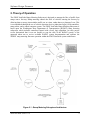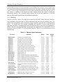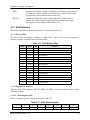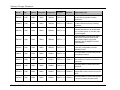
1
SunGuideTM: Ramp Metering Firmware Software Design Document SunGuide-RMF-SDD-1.0.4 Prepared for: Florida Department of Transportation Traffic Engineering and Operations Office 605 Suwannee Street, M.S. 90 Tallahassee, Florida 32399-0450 (850) 410-5600 March 5, 2009 Software Design Document Document Control Panel File Name: SunGuide-RMF-SDD-1.0.4 File Location: SunGuide CM Repository CDRL: n/a Created By: Reviewed By: Modified By: Name Initial Date John Brisco, SwRI® JSB 02/28/07 Steve Sprouffske, SwRI SJS 03/05/07 Bruce Farmer, SwRI SBF 03/07/07 Steve Dellenback, SwRI SWD 03/09/07 Steve Dellenback, SwRI SWD 04/06/07 Steve Dellenback, SwRI SWD 06/06/07 Steve Dellenback, SwRI SWD 03/17/08 Steve Dellenback, SwRI SWD 03/05/09 Steve Sprouffske, SwRI SJS 04/05/07 Bruce Farmer, SwRI SBF 04/05/07 Steve Sprouffske, SwRI SJS 05/29/07 Bruce Farmer, SwRI SBF 05/30/07 Steve Sprouffske, SwRI SJS 03/11/08 MCA 03/04/09 Marc Alban, SwRI Completed By: SunGuide-RMF-SDD-1.0.4 i Software Design Document Table of Contents Page List of Tables ................................................................................................................ iv List of Figures ............................................................................................................... v Acronyms ...................................................................................................................... vi Revision History .......................................................................................................... vii 1. Scope ................................................................................................... 1 1.1 1.2 1.3 1.4 Document Identification ............................................................................... 1 Project Overview ........................................................................................... 1 Related Documents ....................................................................................... 1 Contacts ......................................................................................................... 2 2. Theory of Operation ............................................................................ 4 3. High Level Design ............................................................................... 6 3.1 Subsystem Components .............................................................................. 6 3.1.1 Hardware Interface .......................................................................... 6 3.1.2 Data Surveillance ............................................................................ 8 3.1.3 Metering .......................................................................................... 9 3.2 Error Handling ............................................................................................. 13 4. Hardware Notes ................................................................................. 15 4.1 General Notes .............................................................................................. 15 4.2 Switches and Indicators ............................................................................. 15 4.2.1 ACTIVE LED ............................................................................... 15 4.2.2 LOCATION DIP Switches ........................................................... 15 4.2.3 FEATURE DIP Switches .............................................................. 15 4.2.4 32K/128K BYTE PROM jumper.................................................. 15 4.2.5 64K BYTE PROM jumper ............................................................ 15 4.2.6 MAP1 and MAP2 jumpers ............................................................ 15 4.2.7 EXT/INT jumper ........................................................................... 16 4.2.8 SWAP ACIAS jumper .................................................................. 16 4.2.9 MODE A headerless jumper ......................................................... 16 4.2.10 MODE B headerless jumper ......................................................... 16 4.2.11 RTC headerless jumper ................................................................. 16 4.2.12 PTA0 headerless jumper ............................................................... 16 4.2.13 PTG1 headerless jumper ............................................................... 16 4.3 System Clock............................................................................................... 16 4.4 System Memory Map .................................................................................. 16 4.5 Memory-Mapped Registers ........................................................................ 17 4.5.1 System Status Register .................................................................. 17 4.6 Interrupts ..................................................................................................... 18 4.7 Down Time Accumulator ............................................................................ 19 SunGuide-RMF-SDD-1.0.4 i Software Design Document 4.8 Digital I/O Interface ..................................................................................... 19 4.9 Keyboard Interface ...................................................................................... 19 4.10 Display Interface ......................................................................................... 19 4.10.1 Call Lights ..................................................................................... 20 4.10.2 7-SEGMENT DISPLAYS ............................................................ 20 4.11 ACIA Interface ............................................................................................. 22 4.11.1 Memory Map ................................................................................. 22 4.11.2 Register Descriptions .................................................................... 22 4.11.3 Expected ACIA Configuration...................................................... 24 4.12 Address Decoding ...................................................................................... 24 4.12.1 Base Address Decoder (GAL16V8 PLD) ..................................... 25 4.12.2 I/O Address Decoder (GAL16V8 PLD) ....................................... 25 4.13 Data Dictionary ............................................................................................ 27 5. Interfaces ........................................................................................... 37 6. Traceability ........................................................................................ 38 List of Appendices Appendix A - Digital Input Port Mappings Appendix B - Digital Output Port Mappings SunGuide-RMF-SDD-1.0.4 ii Software Design Document List of Tables Page Table 3.1 - Metered Lane Parameters ............................................................................................. 9 Table 4.1 - Program Memory Map ............................................................................................... 16 Table 4.2 - Data Memory Map ..................................................................................................... 17 Table 4.3 - Hardware Interrupt Sources ........................................................................................ 18 Table 4.4 - Assigned Interrupt Vectors ......................................................................................... 18 Table 4.5 - Keypad Mapping (I/O Address 7407h) ...................................................................... 19 Table 4.6 - Call Light Mapping (I/O Address 740Ah) ................................................................. 20 Table 4.7 - Call Light Mapping (I/O Address 7408h) .................................................................. 20 Table 4.8 - 7-Segment Display Decode Table .............................................................................. 20 Table 4.9 - 7-Segment Mapping (I/O Address 7408h) ................................................................. 21 Table 4.10 - 7-Segment Mapping (I/O Address 7409h) ............................................................... 21 Table 4.11 - ACIA Memory Map ................................................................................................. 22 Table 4.12 - ACIA Status Register ............................................................................................... 22 Table 4.13 - ACIA Control Register ............................................................................................. 23 Table 4.14 - ACIA Receive Data Register.................................................................................... 24 Table 4.15 - ACIA Transmit Data Register (TDR) ...................................................................... 24 Table 4.16 - Base Address Decoder Signals ................................................................................. 25 Table 4.17 - I/O Address Decoder Signals ................................................................................... 25 Table 4.18 - Global Parameters .................................................................................................... 27 Table 4.19 - Lane 1 Parameters .................................................................................................... 28 Table 4.20 - Lane 2 Parameters .................................................................................................... 29 Table 4.21 - Lane 3 Parameters .................................................................................................... 30 Table 4.22 - Time of Day Table Data ........................................................................................... 31 Table 4.23 - Data Status Packet .................................................................................................... 32 Table 4.24 - Volume Data ............................................................................................................. 34 Table 4.25 - Occupancy Data........................................................................................................ 35 Table 4.26 - Occupancy Data cont. ............................................................................................... 36 SunGuide-RMF-SDD-1.0.4 iii Software Design Document List of Figures Page Figure 1.1 - High-Level Architectural Concept .............................................................................. 1 Figure 2.1 - Ramp Metering Subsystem Architecture .................................................................... 4 SunGuide-RMF-SDD-1.0.4 iv Software Design Document List of Acronyms ACIA ..........................Asynchronous Communications Interface Adapter ADDR ........................Address BLPI ...........................Phase/Interval Blanking line BLTIM .......................Time Blanking line CDS ............................Counter Divide Select CPU ............................Central Processing Unit CR ..............................Control Register CTS ............................Clear To Send DCD ...........................Data Carrier Detect DOT ...........................Department of Transportation DP ..............................Decimal Point display line DTA ...........................Down Time Accumulator FDOT .........................Florida Department of Transportation FE ...............................Framing Error GENCS ......................General-Purpose Internally Generated and Configurable Chip-Select HOV ...........................High Occupancy Vehicle I/O ..............................Input/Output IRQ.............................Interrupt Request ITN .............................Invitation to Negotiate ITS..............................Intelligent Transportation Systems LED ............................Light Emitting Diode MCU ..........................Multipoint Control Unit MSB ...........................Most Significant Bit PAL ............................Process Asset Library PE ...............................Parity Error PLD ............................Programmable Logic Device RAM ..........................Random Access Memory RDR ...........................Receive Data Register RDRF ........................Receive Data Register Full RIE .............................Receiver Interrupt Enable RMF ...........................Ramp Metering Firmware ROV ...........................Receiver Overrun SDD............................Software Design Document SR...............................Status Register SwRI ..........................Southwest Research Institute® TC ..............................Transmitter Control TDR............................Transmit Data Register TDRE .........................Transmit Data Register Empty TOD ...........................Time-Of-Day VPM ...........................Vehicles Per Minute W3 ..............................World Wide Web Consortium WS..............................Word Select WsDOT ......................Washington State Department of Transportation SunGuide-RMF-SDD-1.0.4 v Software Design Document Revision History Revision Date Changes 1.0.0 March 14, 2007 Initial Release. 1.0.1 April 6, 2007 Added Detector and Input Echo to the firmware parameters table in the Lane 1 parameters page. Added E Page Entry to the firmware parameters table in the Global parameters page. Added C, E and F page designators for each of the tables in the data dictionary. 1.0.2 June 5, 2007 In the data dictionary memory maps, moved the memory locations for detector echo and input echo from the F1 Page to the C Page. In the data dictionary memory maps, modified the tables to shade the read-only entries. In the data dictionary memory maps, removed entries and tables that are not used by the RM firmware. In the Appendix B Digital Output Port Mappings table, swapped the outputs used for the Metering light emitting diode (LED) and Signal Light 3 Yellow so that the Metering LED is output on C1 connector pin 8. 1.0.3 March 17, 2008 Modified text in the Volume Adjust description to accurately reflect the algorithm functionality. 1.0.4 March 5, 2009 Updated for Footprint issues #1050, #1076 and #1079 SunGuide-RMF-SDD-1.0.4 vi Software Design Document 1. Scope 1.1 Document Identification This document serves as the Software Design Document (SDD) for the Florida Department of Transportation (FDOT) Ramp Metering firmware. 1.2 Project Overview The FDOT is conducting a program that is developing SunGuide software. The SunGuide software is a set of Intelligent Transportation System (ITS) software that allows the control of roadway devices as well as information exchange across a variety of transportation agencies. The goal of the SunGuide software is to have a common software base that can be deployed throughout the State of Florida. The SunGuide software development effort is based on ITS software available from both the States of Texas and Maryland; significant customization of the software is being performed as well as the development of new software modules. The following figure provides a graphical view of the SunGuide software: Figure 1.1 - High-Level Architectural Concept The SunGuide development effort spans approximately two years. After the development, the software will be deployed to a number of districts and expressway authorities throughout Florida, and support activities will be performed. 1.3 Related Documents The following documents were used to develop this document: SunGuide-RMF-SDD-1.0.4 1 Software Design Document SwRI Qualification Response: Response to the Invitation to Negotiate (ITN): Statewide Transportation Management Center Software Library System, Negotiation Number: ITNDOT-02/03-9025-RR, SwRI Proposal No. 10-35924, dated: November 18, 2002. SwRI Technical Proposal: Technical Proposal for Invitation to Negotiate (ITN): Statewide Transportation Management Center Software Library System, Negotiation Number: ITN-DOT-02/03-9025-RR, SwRI Proposal No. 10-35924, dated: January 31, 2003. SwRI Cost Proposal: Cost Proposal for Invitation to Negotiate (ITN): Statewide Transportation Management Center Software Library System, Negotiation Number: ITNDOT-02/03-9025-RR, SwRI Proposal No. 10-35924, dated: January 31, 2003. SwRI BAFO letter: Southwest Research Institute Proposal No. 10-35924, “Invitation to Negotiate (ITN): Statewide Transportation Management Center Software Library System”, Reference: Negotiation Number: ITN-DOT-02/03-9025-RR, dated: May 5, 2003. FDOT procurement document: Invitation to Negotiate (ITN), Negotiation Number: ITNDOT-02/03-9025-RR, Statewide Transportation Management Center Software Library System, dated: October 21, 2002. FDOT Scope of Services: Statewide Transportation Management Center Software Library System: Scope of Services, September 22, 2003. FDOT Requirements Document: Statewide Transportation Management Center Software Library System: Requirements Specification, June 3, 2003. Southwest Research Institute, TMC Software Study, November 15, 2001. Southwest Research Institute, Introduction to an Operational Concept for the Florida Statewide Library, FDOT – OCD – 1.0, March 31, 2002. Washington State Department of Transportation, Ramp Meter / Data Collection User’s Manual, Version 4.47, January 28, 2005. World Wide Web Consortium (W3) website: http://www.w3.org. SunGuide Project website: http://sunguide.datasys.swri.edu. 170 Communication Protocol, VAX-170-DOC05, Washington State Dept. of Transportation, September 3, 2002. 1.4 Contacts The following are contact persons for the SunGuide software project: Elizabeth Birriel, ITS Central Office, [email protected], 850-410-5606 Trey Tillander, FDOT SunGuide Project Manager, [email protected], 850410-5617 Khue Ngo, Senior ITS Analyst, [email protected], 850-410-5579 David Chang, PBS&J Project Manager, [email protected], 850-410-5622 Steve Dellenback, SwRI Project Manager, [email protected], 210-522-3914 Robert Heller, SwRI Software Project Manager, [email protected], 210-522-3824 SunGuide-RMF-SDD-1.0.4 2 Software Design Document SunGuide-RMF-SDD-1.0.4 3 Software Design Document 2. Theory of Operation The FDOT SunGuide Ramp Metering Subsystem is designed to manage the flow of traffic from ramps onto a freeway. Ramp metering controls the flow of vehicles entering the freeway by allowing them to merge into mainline traffic one at a time, rather than as a platoon of cars. This is accomplished through the use of vehicle detection devices (induction loops), field controllers, ramp meters, and a central computer system. The FDOT SunGuide Ramp Metering Subsystem is based upon the Washington State Department of Transportation (WsDOT) ramp metering subsystem, which includes centralized control with a fuzzy logic algorithm. An early project review determined that it was not feasible to port the code of the WsDOT system, so the approach taken was to review available WsDOT system documentation and replicate the WsDOT ramp metering firmware operation within the FDOT SunGuide system architecture. Figure 2.1 - Ramp Metering Subsystem Architecture SunGuide-RMF-SDD-1.0.4 4 Software Design Document The SunGuide system will make use of traffic information received from the detectors and by using the Fuzzy Logic Ramp Metering algorithm at Central. The data inputs to the fuzzy-logic algorithm are: a) Mainline occupancy just before the ramp outlet, b) Mainline speed just before the ramp outlet, c) Ramp queue occupancy, e) Advance Queue detector occupancy, f) High Occupancy Vehicle (HOV) bypass volume, g) Downstream speed from assigned one or more detector station(s), and h) Downstream occupancy from one or more assigned detector station(s). The output from the Fuzzy Logic algorithm will be metering rate in vehicles/20 seconds. SunGuide-RMF-SDD-1.0.4 5 Software Design Document 3. High Level Design The FDOT Ramp Meter Firmware operates on a Model 170 Controller. The firmware utilizes 2 serial interfaces (asynchronous communications interface adapters [ACIAs]). The firmware processes accumulated data from as many as 40 detectors. The program also processes speed, length, and vehicle classification from up to 8 dual-detector speed traps. The firmware has the capability to meter up to three ramps independently. The FDOT Ramp Meter Firmware has two communications modes: central or local control. In central mode, configuration parameters are sent from the central system to the controller. The central system periodically polls for surveillance and metering data. In local mode, previously downloaded parameters or user input parameters are used for surveillance and metering functions. Parameters are viewable via the front panel keypad. Communications with Central requires the manual entry of the communications address. 3.1 Subsystem Components The FDOT Ramp Meter Firmware is designed as a three- function program. The functions consist of functionality segmented by hardware interface, data surveillance, and ramp metering. A detailed description of the segment functionality is described in the following paragraphs. 3.1.1 Hardware Interface 3.1.1.1 Digital Inputs The ramp meter controller incorporates six digital input ports with eight bits of inputs per port. The input ports are memory mapped into the central processing unit (CPU) address space as defined in Section 4.8. The digital inputs are used to monitor the status of the 40 loop detectors and the police switch. The input port mappings are defined in Appendix A. The system software monitors the states of the detectors to calculate speed, volume, and occupancy for the metering algorithms. 3.1.1.2 Digital Outputs The ramp meter controller incorporates seven digital output ports with eight bits of outputs per port. The output ports are memory mapped into the CPU address space as defined in Section 4.8. The digital outputs are used to control the states of the signal lights for each of the three ramps. They are also used to reflect the status of the front panel call lights for the watchdog and to initiate a detector reset. The output port mappings are defined in Appendix B. 3.1.1.3 Keypad The ramp meter controller incorporates a 16-key keypad for user input. The keypad interface is memory mapped into the CPU address space as defined in Section 4.9. The system software continually monitors the keypad for key actuations. The keypad is used to view and modify the operational configuration of the ramp meter controller. The usage of the keypad for this purpose is described in the Ramp Metering Firmware Software User’s Manual. SunGuide-RMF-SDD-1.0.4 6 Software Design Document 3.1.1.4 LED Display The ramp meter controller incorporates six 8-segment LEDs for displaying numeric values. The LED interface is memory mapped into the CPU address space as defined in Section 4.10. The LEDs are used for two different operation modes. When the keypad is used to view or modify the ramp meter configuration parameters, the LEDs are used to display numeric values entered by the user or parameter values viewed by the user. The function of the LEDs in keypad entry mode is described in the Ramp Metering Firmware Software User’s Manual. When the keypad is not being used, the LEDs are used to display operational status of the each of the three metered lanes. A single LED (the Phase LED) is used to indicate the current ramp ID (1-3). A second LED (the Interval LED) is used to indicate the current metering status according to the value displayed. The metering statuses for the LED value displayed are described in the Ramp Metering Firmware Software User’s Manual. The last four LEDs (the Timing LEDs) are used to display the current metering cycle time for the ramp. 3.1.1.5 Call Lights The ramp meter controller incorporates nine call lights (single LEDs) to display operational status information. The call light interface is memory mapped into the CPU address space as defined in Section 4.10. The call lights are used for two different operation modes. When the keypad is used to view or modify the ramp meter configuration parameters, the call lights are used to indicate values entered by the user or parameter values viewed by the user. The function of the call lights in keypad entry mode is described in the Ramp Metering Firmware Software User’s Manual. When the keypad is not being used, the call lights are used to reflect system operational status. The function of each of the call lights in this mode is described in the Ramp Metering Firmware Software User’s Manual. 3.1.1.6 Asynchronous Communication Interface Adapter (ACIA) The ramp meter controller incorporates two ACIAs. The ACIA interfaces are memory mapped into the CPU address space as defined in Section 4.11. ACIA1 is used for serial communications to the host computer. The host computer uses the serial interface to issue commands to the ramp meter controller to configure and control the operation of the system software. The host computer also uses the serial interface to poll for data collected by the controller software (e.g., speed, volume and occupancy). The communications protocol to the host computer is designed according the protocol defined in the 170 Communication Protocol VAX-170-DOC05 produced by the Washington State Department of Transportation. ACIA2 is configured in loop-back fashion to generate a time base for collecting speed trap data. The ACIA is configured to generate an interrupt when the transmit data register shifts data out and is configured for a baud rate of 19.2 KB. This interrupt is used to sample data for each of the eight possible speed traps in round robin fashion on every other interrupt. This results in a sample rate of 8.333 ms, or 120 Hz, for each speed trap. SunGuide-RMF-SDD-1.0.4 7 Software Design Document 3.1.2 Data Surveillance The data surveillance function of the Ramp Metering Firmware (RMF) performs three main tasks: volume and occupancy data collection, speed trap calculations, and data validation. Data calculations are stored every 20 seconds and over-written every minute. This provides the firmware with a rolling one minute data set. Data poll responses are packaged with the current 20 second data set. 3.1.2.1 Data Collection Data collection functions process data from up to 40 configurable detectors. Parameters sent from Central or manually input define the source and purpose of the inputs. The core purpose of all detectors is to provide volume and occupancy. This data is reported every 20 seconds in response to a poll request. The C1 connector links the detector inputs to the controller. Each detector is mapped to a pin assignment. The detector actuations occur when the appropriate pin is grounded. The controller firmware scans the pins on a 60Hz cycle. The firmware calculates the number of scans each pin is grounded over a 20 second period. The maximum number of scans in a 20 second period is 1200. Occupancy is calculated as the following: Occupancy = scans / 12. Volume is calculated as the number of times the detector state changes from actuated to non-actuated. 3.1.2.2 Speed Trap Speed calculations are computed from the 8 configurable dual-detector traps. Two detectors are installed in a lane at a defined distance apart. These detectors are scanned by the speed trap algorithm 120 times a second. The speed trap algorithm calculates the number times the upstream detector is actuated while the downstream detector remains non-actuated. The speed trap length divided by the scan count of the upstream detector provides the vehicle speed. Vehicles can be classified into any one of 4 bin lengths. The vehicle is classified into the largest bin that is greater than the vehicle’s length. Length is calculated by taking the occupancy of the upstream detector multiplied by the speed minus the length of the detector. 3.1.2.3 Data Validation Data validation falls into two areas: data surveillance validation and speed data validation. Data validity flags are set when an error is verified. These flags are reported in the data packet sent in the data poll response message to central. Data surveillance processes valid data in pre-defined volume and occupancy envelopes. For a given volume a minimum and maximum occupancy must be calculated. The firmware has 4 defined occupancy envelopes. When volume exceeds 17 vehicles per minute, the firmware sets the chatter flag. The firmware also monitors for minimum presence or absence known as “Short Pulse.” For presence less than a 1/15 second the accumulated volume and occupancy are ignored for the current actuation. In the case of absence less than 1/15 second, volume is reduced by one count and the occupancy is increased scan for scan to compensate. SunGuide-RMF-SDD-1.0.4 8 Software Design Document Speed validity monitors several invalid data scenarios. When the occupancy ratio is greater than 10% between the upstream and downstream detector, the speed data is thrown out for the current vehicle. Two in a trap is calculated as a second vehicle entering the trap before the first exits. A lost vehicle is defined as the speed trap timer expiring before the vehicle actuates the downstream detector. The calculated speed exceeds the speed limit parameters set by the operator. The length is greater than the predefined length limit. 3.1.3 Metering There are two basic sources for ramp meter control by the FDOT Ramp Metering Firmware: local algorithms using local data or central algorithms using data from the mainline lanes. The central source is normally used for metering, except in special cases and after a communication failure. In special cases the operator commands the controller to meter using the local algorithms, and after a communication failure the controller meters using the local algorithms by default. The basic metering algorithms and metering rate adjustments are controlled by a set of parameters, shown in Table 3.1, sent by the host computer. There is a set of parameters for each metered ramp. Table 3.1 - Metered Lane Parameters Parameter MultiLaneSplit TableRate1 TableRate2 TableRate3 TableRate4 TableRate5 TableOcc1 TableOcc2 TableOcc3 TableOcc4 TableOcc5 MaxMeterRate MinMeterRate QOccThresh1 QOccThresh2 QOccTimer1 QOccTimer2 QOccAdjust1 QOccAdjust2 AdvQOccThresh AdvQOccTimer AdvQOccOverride LongStopTime RedViolationDelay NormalYellow HOVRedDelay Definition Percentage for TOD distribution First rate value in meter rate table Second rate value in meter rate table Third rate value in meter rate table Fourth rate value in meter rate table Last rate value in meter rate table First occupancy value in meter rate table Second occupancy value in meter rate table Third occupancy value in meter rate table Fourth occupancy value in meter rate table Last occupancy value in meter rate table Maximum meter rate Minimum meter rate Queue occupancy threshold to begin adjustment Queue occupancy threshold to terminate adjustment Timer to implement first queue adjustment Timer to implement second queue adjustment First meter rate increment for queue adjustment Second meter rate increment for queue adjustment Occupancy threshold to begin advanced queue override Timer to implement advanced queue override Meter rate adjustment for advanced queue override Passage occupancy time to trigger long stop green Delay time added to red time for red violations Duration of yellow interval of meter cycle Minimum red time for HOV bypass SunGuide-RMF-SDD-1.0.4 Range Units Default Value 0-100 0.0-25.5 0.0-25.5 0.0-25.5 0.0-25.5 0.0-25.5 0-100 0-100 0-100 0-100 0-100 0.0-25.5 0.0-25.5 0-100 0-100 0.0-25.5 0.0-25.5 0.0-25.5 0.0-25.5 0-100 percent VPM VPM VPM VPM VPM percent percent percent percent percent VPM VPM percent percent minutes minutes VPM VPM percent 100 18.0 16.0 13.0 10.0 7.0 15 17 19 21 23 20.0 5.0 30 25 1.0 3.0 2.0 4.0 25 0-255 0.0-25.5 0.0-25.5 0.0-25.5 0.0-25.5 0.0-25.5 seconds VPM seconds seconds seconds seconds 80 12.0 2.0 1.0 0.0 0.0 9 Software Design Document ShortStopQOcc QStartMeterGap Queue occupancy to trigger short stop green Gap required at queue detector for startup red 0-100 0.0-25.5 percent seconds 15 3.0 3.1.3.1 Basic Metering Algorithms Time-of-Day (TOD) Metering Rate The TOD Rate table contains 32 events that can be activated on any combination of days of the week. Each event has a starting hour and minute, flags for effective days of the week, and an associated metering rate. The metering rate is in the range of 0-25.5 Vehicles Per Minute (VPM), where a value of 0 will cause a Stop Metering event and a non-zero value will cause a Start Metering event, setting the TOD Metering Rate to the value. A value of 255 (25.5) will cause the TOD Metering Rate to be ignored in favor of the Traffic Metering Rate. The TOD table controls all active ramps in the controller. The rate from the TOD table is multiplied by the ramp MultiLaneSplit parameter to determine the TOD rate for that ramp. The multilane spilt values for all active ramps in a controller do not have to total 100. A power failure of more than 4 hours and 15 minutes will prevent use of the TOD table to control metering. The controller must receive a time value from the host computer before the TOD metering control can be resumed. Traffic Metering Rate The Traffic Metering Rate is based on mainline occupancy. The traffic algorithm calculates the Traffic Metering Rate using the one minute moving average occupancy of the defined mainline detectors. The one minute moving average mainline occupancy is compared to the occupancy levels in the TableOcc1-5 and TableRate1-5 parameter tables. The occupancy/rate pairs specify points on a metering rate vs. mainline occupancy slope. Linear interpolation is used to calculate a metering rate from a given occupancy value. The MaxMeterRate parameter is used if the input occupancy is less than the lowest table entry, and the MinMeterRate parameter is used if the occupancy is greater than the highest table entry. Intermediate Meter Rate The Intermediate Metering Rate is the more restrictive of the TOD Metering Rate and the Traffic Metering Rate when in Local mode, and is the Traffic Metering Rate when in Central mode. Fuzzy Meter Rate A Fuzzy Metering Rate is provided by the host system for each of the metered ramps. A nonzero Fuzzy Metering Rate will always be used when in Central mode, and no adjustments or overrides are applied to it. 3.1.3.2 Metering Rate Adjustments Once the basic metering algorithms determine the Intermediate Meter Rate, it is adjusted to account for specific ramp conditions. These adjustments are described below. Queue Adjusted Metering Rate If the 20-second queue detector occupancy exceeds the QOccThresh1 parameter for more than QOccTimer1 parameter minutes, the Intermediate Metering Rate is adjusted upward by the QOccAdjust1 parameter. If the 20-second queue detector occupancy exceeds the QOccThresh1 parameter for more than QOccTimer2 parameter minutes, the Intermediate Metering Rate is SunGuide-RMF-SDD-1.0.4 10 Software Design Document adjusted upward by the QOccAdjust2 parameter instead. The adjustment will remain in effect until the 20-second queue detector occupancy is less than or equal to the QOccThresh2 parameter for one minute. If an intermediate queue detector is used, its 20 second occupancy is used with the same thresholds, timers, and adjustment values. Adjustments due to intermediate queue detector occupancy are added to the adjustments from the queue detector occupancy. The Intermediate Metering Rate with queue and intermediate queue adjustments applied is called the “Queue Adjusted Metering Rate.” While either the queue detector adjustment or the intermediate queue detector adjustment is in effect, the queue adjustment alarm is set. Volume Adjustment The ramp volume is used to adjust the Queue Adjusted Metering rate due to red signal violations on the ramp. The Queue Adjusted Metering Rate is reduced by the sum of the red signal violations in the last three 20 second periods. Advanced Queue Override If queue adjustment is in effect and the one-minute moving average occupancy of either left or right advance queue detector exceeds the AdvQOccThresh parameter value for more than AdvQOccTimer parameter seconds, the Queue Adjusted Metering rate is further adjusted by the AdvQOccOverride parameter value. If both advanced queue detector occupancies exceed the threshold, the override values are additive. The advanced queue override remains in effect until the one-minute moving occupancy of the advance queue detector drops below the AdvQOccThresh parameter value. High-Occupancy Vehicle Bypass Meter Rate Adjustment For each actuation of the HOV demand detector or ramp demand detector while the metered lane signal is red, the remaining red signal time of the cycle is compared to the HOVRedDelay parameter value, and the larger value is used as the remaining red time. Red Signal Violations For each actuation of the passage detector during the red signal portion of the cycle, the red signal cycle time is incremented by RedViolationDelay parameter value. Adjusted Meter Rate The Adjusted Metering rate is the basic meter rate adjusted for queue occupancy, adjusted for HOV bypass traffic, adjusted for red signal violations, and adjusted for advanced queue detector occupancy. Finally, the Adjusted Metering rate is bounded by the MinMeterRate and MaxMeterRate parameter values. Cycle Length A new cycle length, in seconds, is computed from the selected metering rate, which is expressed in VPM. The selected metering rate will be the Fuzzy Metering rate if it is non-zero; otherwise, the Adjusted Metering rate will be used. SunGuide-RMF-SDD-1.0.4 11 Software Design Document 3.1.3.3 Failure Adjustments Although all detectors can be failed by a watchdog timer due to inactivity, the demand and passage detectors can also be failed by the metering software. The demand detector for a metered ramp will be failed if two consecutive passage detector actuations occur without any presence on the demand detector. The passage detector for a metered ramp will be failed if two consecutive demand detector actuations occur without any presence on the passage detector. A failed demand detector causes metering to be stopped for the affected ramp. A failed passage detector will cause the use of a fixed 1.5 second green time per allowed vehicle for each demand detector actuation. A failed queue detector will prevent the use of queue detector and advance queue detector occupancy metering adjustments. If the demand detector fails in the actuated state and has not been failed by the watchdog timer, metering will continue as if a continuous demand is present. Normally an activation of the demand detector must occur before the signal light can cycle to green. A short stop condition occurs when a vehicle stops before reaching the demand detector. In this case the signal light will remain red until the cycle times out and the occupancy of the queue detector exceeds the ShortStopQOcc parameter value. The short stop condition will cause the signal to cycle to green until a passage is detected. Normally an activation of the passage detector is used to cycle the signal light from green back to yellow or red. A long stop condition occurs when a vehicle crosses the stop line and causes a premature passage detector actuation. In this case the signal light will remain red until the cycle times out and the LongStopTime parameter value is reached. The long stop condition will cause the green signal to be timed. A fixed 1.5 seconds per allowed vehicle will be used. 3.1.3.4 Start Metering Metering is started by a command from the host computer if in Central mode or by the current time matching an entry in the TOD table with a non-zero metering rate if in Local mode. Metering will not be started if the demand detector of a metered lane is failed. The sequence of events is described in the following list. 1. A 20-second lead-in green period is started by setting the signal light to green. 2. A gap in the occupancy of the queue detector is found that matches the QStartMeterGap parameter value. 3. If a startup yellow time is defined, transition to a startup yellow period by setting the signal light to yellow. 4. Transition to an initial red period by setting the signal light to red. The signal light will remain red until all of the following conditions are satisfied. 1. The demand detector is actuated or a short-stop condition exists. 2. The cycle time has ended, including any delays added by the HOV bypass delay or red signal violations. 3. The passage detector is not activated. 4. The red signal light has been on for a minimum of one second. SunGuide-RMF-SDD-1.0.4 12 Software Design Document 3.1.3.5 Stop Metering Metering is stopped by command from the host computer if in Central mode or by the current time matching an entry in the TOD table with a zero metering rate if in Local mode. The sequence of events is described in the following list. 1. A gap in the demand detector is found that matches the DemandEndGap parameter value. 2. The gap length is reduced by 0.1 second every 6.0 seconds until a gap is found. 3. The signal will rest in green for the amount of time specified by the MeterEndGreen parameter. 4. The signal will go dark or rest in green dependent on the MeterOffDisplay parameter. 3.1.3.6 Metering Preemption Metering preemption can be initiated locally via a cabinet police switch and remotely via the preempt parameter. If the pre-empt parameter is non-zero or the police switch is closed, the controller outputs a steady green signal on all ramps. When the switch is re-opened or the preempt parameter set to 0, the controller will return to its previous metering state. 3.1.3.7 Metering Sequence Green Interval The start of a new metering cycle begins with the green signal state. Normally the green interval terminates when the passage detector has been actuated for each vehicle allowed per green cycle. If the passage detector has failed or a short green condition is in effect, the green interval will be 1.5 seconds for each vehicle allowed per green cycle. There is no minimum green time, but there will be at least a half second gap between the start of a green cycle on any two ramps controlled by the same controller. Yellow Interval The yellow interval will begin with the end of the green interval if the NormalYellow parameter has a value greater than zero. There is no minimum value for the yellow interval. Red Interval The red interval begins after the green or yellow interval and uses the remainder of the current cycle time. The minimum red interval is one second, but it can be extended by HOV bypass delay or red signal violations. 3.2 Error Handling During operation the ramp meter controller will detect various errors. These errors occur when detectors fail or errors occur during communications processing. There are several different methods errors are reported to the system. A flag is sent in a data message to alert the central system to request an error report. Failed detector or data validation flags are set in data messages to alert central system that detectors have failed. The following is a list of potential errors reported by the controller: • Detector Failure • Loop Locked ON/OFF • Conflict Monitor Tripped SunGuide-RMF-SDD-1.0.4 13 Software Design Document • • • • • Police Switch Active Memory Check Error Short Pulse Chatter (> 3 counts/second) Outside Vol/Occ Envelope SunGuide-RMF-SDD-1.0.4 14 Software Design Document 4. Hardware Notes The FDOT Ramp Meter Firmware is designed to operate on a Model 170E Controller. The Ramp Meter system is designed to manage ramp traffic for up to 3 metering ramps. The controller has 40 configurable input loops and 96 defined outputs. Communications with the controller are via a serial-based connection. 4.1 • • • • • 4.2 General Notes Current board is Rev D. Microprocessor clock is 8MHz. External 9.8304 MHz oscillator used for interfacing to 2070-style front panel at 38.4K baud and for ACIA baud rate generation. Rev D of board corrects an error on A4 (divide-by-five counter for baud rate generation) of Rev C board. This may have just been a layout error. Rev E of board appears to only have silkscreen changes, so firmware should work in Rev D or Rev E boards, and may also work in Rev C boards. Switches and Indicators This section describes the switches and indicators on the board. 4.2.1 ACTIVE LED This LED is used to indicate that the system firmware is operating properly. The LED is controlled by PTG2 (Port G, bit 2). 4.2.2 LOCATION DIP Switches This bank of switches is read at PA0-PA7 (Port A). Currently all switches are ON. 4.2.3 FEATURE DIP Switches This bank of switches is read at PE0-PE7 (Port E). Currently all switches are ON. 4.2.4 32K/128K BYTE PROM jumper This jumper controls address line A15 of the PROM. If the jumper is in place, A15 is always high. Should NOT be in place if the 64K jumper is in place. 4.2.5 64K BYTE PROM jumper This jumper controls address line A15 of the PROM. If the jumper is in place, A15 is controlled by the BANK signal from the microcontroller (PG0 - Port G, bit 0). Should NOT be in place if the 32K/128K jumper is in place. 4.2.6 MAP1 and MAP2 jumpers These jumpers place the system in special ‘non-standard’ system address decoding operating modes. These jumpers are not in place. SunGuide-RMF-SDD-1.0.4 15 Software Design Document 4.2.7 EXT/INT jumper This jumper has one of two positions. INT(CPU MEM) provides a logic LOW to the BASE ADDRESS DECODER chip at A22. EXT(DPRM/MEM) presents a logic HIGH. This is currently jumpered to INT. In this mode, Dual Port Random Access Memory (RAM) is disabled. 4.2.8 SWAP ACIAS jumper If this jumper is in place, a physical-to-logical swapping of ACIAs 2 and 3 occurs. This jumper is for support of dual modem configurations. 4.2.9 MODE A headerless jumper This jumper controls the state of the MODA/LIR input pin of the 68HC11. This jumper is not in place, resulting in a HIGH logic level on the input pin. 4.2.10 MODE B headerless jumper This jumper controls the state of the MODB/STDBY input pin of the 68HC11. This jumper is not in place, resulting in a HIGH logic level on the input pin. 4.2.11 RTC headerless jumper This jumper controls a special RTCIN pulse interrupt feature. This jumper is not in place, so the feature is disabled. 4.2.12 PTA0 headerless jumper This jumper controls the logic level input to pin PA0 on the microcontroller. This jumper is in place, causing the logic level to be controlled by the state of DIP switch 1 on the LOCATION switch block. If sw1 is ON, PA0 will be HIGH, and vice versa. 4.2.13 PTG1 headerless jumper This jumper controls the logic level input to pin PG1 on the microcontroller. This jumper is not in place, resulting in a LOW logic level at PG1. If the jumper was in place, it would cause the logic level to be controlled by the state of DIP switch 1 on the LOCATION switch block. If sw1 was ON with the jumper in place, PG1 would be HIGH, and vice versa. 4.3 System Clock The multipoint control unit (MCU) system clock input is 9.8304MHz. This clock input must be internally divided by 4 to produce a system E clock rate of 2.4576MHz. 4.4 System Memory Map The system memory map for the board as it is presently configured is as follows: Table 4.1 - Program Memory Map ADDRESS FUNCTION SIZE IN BYTES 8000 - FFFF PROM 32K SunGuide-RMF-SDD-1.0.4 16 Software Design Document Table 4.2 - Data Memory Map ADDRESS FUNCTION SIZE IN BYTES 0000 - 6FFF NVRAM 28K 7000 LOCATION SWITCH 1 7001 MCU REGISTERS 1 7002 PORT G 1 7003 - 7009 MCU REGISTERS 7 700A FEATURE SWITCH 1 700B - 705F MCU REGISTERS 85 7060 – 73FF VOLATILE CPU RAM ~1K 7400 DTA MINUTES 1 7401 – 740A I/O 10 740B – 740E Not Used 4 740F DTA SECONDS 1 7410 – 7411 ACIA1 2 7412 – 7413 ACIA2 2 7414 – 7415 ACIA3 2 7416 – 7417 ACIA4 2 7418 - 75FE RESERVED 487 75FF IRQ STATUS PORT (READ) 1 75FF RTC IRQ RESET (WRITE) 1 7600 – 7FF7 NVRAM ~2K 7FF8 – 7FFF NVRAM’s RTC REGISTERS 8 Note: The INIT register on the microcontroller must be programmed with a value of 0x77 within the first 64 clock cycles after a reset to move the microcontroller’s internal RAM and register map to base address 7000h. 4.5 Memory-Mapped Registers 4.5.1 System Status Register The System Status byte is mapped to address 7FFEh for reading. The status register contents are as follows: Bit 7 Bit 6 Bit 5 Bit 4 Bit 3 Bit 2 Bit 1 Bit 0 /RTCIRQ /DTATO BANK EXT/INT /IRQ4 /IRQ3 /IRQ2 /IRQ1 /IRQ1 - /IRQ4 Indicates that a data byte is ready at the corresponding serial port. These flags are automatically reset through the ACIA interface. EXT/INT This bit indicates the status of the board jumper that selects either INT(CPU MEM) or EXT(DPRM/MEM). SunGuide-RMF-SDD-1.0.4 17 Software Design Document BANK This bit is set when the microcontroller firmware sets bit 0 of PortG, which is the BANK bit. This bit is always tied to A16 of the PROM, and will also be tied to A15 if the 64K BYTE PROM jumper is in place. If clear, PROM addresses 0000h-7FFFh map to standard address 8000h-FFFFh. If set, PROM addresses 8000h-FFFFh map to standard address 8000h-FFFFh. /DTATO This bit is set to 0 when the Down Time Accumulator times out. RTCIRQ This bit is set when 60Hz AC line negative zero crossing occurs. A write to the register clears this bit and resets the RTC interrupt generator. 4.6 Interrupts There are 3 sources of hardware interrupts on the 68HC11: /RESET, /XIRQ, and /IRQ. Table 4.3 - Hardware Interrupt Sources IRQ PIN Description /RESET Resets the processor on negative transition. /XIRQ A power fail interrupt providing a 4ms window for saving critical data before the /RESET activates. This line goes high when an application-specific interrupt occurs. There are 5 interrupt sources that are OR’ed to produce a single interrupt, /CIRQ, at the /IRQ pin: /RTCIRQ – Created from 60Hz AC line negative zero crossings. This signal is used by the CPU as the time base for all signal operations. /IRQ /IRQ1 – From Serial Port (ACIA) 1 /IRQ2 – From Serial Port (ACIA) 2 /IRQ3 – From Serial Port (ACIA) 3 /IRQ4 - From Serial Port (ACIA) 4 The following interrupts are used by the firmware. Table 4.4 - Assigned Interrupt Vectors Interrupt Function /RESET Restarts execution of the ramp meter firmware. Clock Monitor Fail Places the system in a safe mode with all signal lights turned off. COP Failure Places the system in a safe mode with all signal lights turned off. Illegal Opcode Trap Places the system in a safe mode with all signal lights turned off. /XIRQ Pin Places the system in a safe mode with all signal lights turned off. /IRQ Used for speed trap processing and serial communications. Real-Time Interrupt Used for miscellaneous RMF interrupt operations. SunGuide-RMF-SDD-1.0.4 18 Software Design Document 4.7 Down Time Accumulator The Down Time Accumulator (DTA) keeps track of the length of time that the controller is down due to low/missing power. The time can be read by the DTA MINUTES and DTA SECONDS memory-mapped registers. The DTA is reset by writing to address 7400h. 4.8 Digital I/O Interface There are 56 bits of digital Outputs (OP0 – OP55). Outputs are set by writing to address range 7401h – 7407H. There are only 48 inputs, however, at addresses 7401h – 7406h. 4.9 Keyboard Interface The keyboard interface for the controller is memory-mapped within the input/output (I/O) space at address 7407h. There does not appear to be any interrupt input into the system for when a key is pressed, so this is most likely a polled interface. There are five signals going out of the keyboard module, called KBMS, KBNMS, KBNLS, KBLS, and KBCON. KBCON is set when a key is pressed. The other four represent a keypad input, where KBMS is Keyboard Most Significant bit, KBNMS is Keyboard Next Most Significant bit, KBNLS is Keyboard Next Least Significant bit, and KBLS is Keyboard Least Significant bit. The 4-bit value represents the keypad value (‘0’ – ‘F’). A Stop Time toggle switch is located on the front panel, and its value is also at address 7407h. The key and switch input mapping is defined below: Table 4.5 - Keypad Mapping (I/O Address 7407h) 7 6 5 4 3 2 1 0 N/A N/A STOP_SW KBMS KBNMS KBNLS KBLS KBCON KBCON This bit is set when a key is pressed and ready to be read from the I/O register. KBMS-KBLS These four bits identify the key that was pressed. 0000b is a ‘0’, and 1111b is an ‘F’. Each key is represented as its corresponding hex value. STOP_SW This bit is set when the front panel Stop Time switch is in the ON position. 4.10 Display Interface The display interface for the controller consists of six 7-segment LED displays and ten individual LED indicators. The seven-segment indicators are called PHASE, INT, MS, NMS, NLS, and LS. PHASE is the upper-left display, and INT is the upper-right display. The four remaining displays form a 4-character display and are arranged below the PHASE/INT in the following order from left to right: MS, NMS, NLS, LS. The decimal point on NLS can be turned on or off. In addition to the 7-segment displays, there are also 10 call light LEDs (CALL0 – CALL9). SunGuide-RMF-SDD-1.0.4 19 Software Design Document 4.10.1 Call Lights The ten-call light LEDs on the front panel are each controlled by a bit in the external I/O address space. Call lights 0-7 are at address 740Ah, and call lights 8 and 9 are at address 7408h. The call light mapping is defined below: Table 4.6 - Call Light Mapping (I/O Address 740Ah) 7 6 5 4 3 2 1 0 CALL7 CALL6 CALL5 CALL4 CALL3 CALL2 CALL1 CALL0 CALL0 CALL1 CALL2 CALL3 CALL4 CALL5 CALL6 CALL7 Set this bit to turn on call light 0. Set this bit to turn on call light 1. Set this bit to turn on call light 2. Set this bit to turn on call light 3. Set this bit to turn on call light 4. Set this bit to turn on call light 5. Set this bit to turn on call light 6. Set this bit to turn on call light 7. Table 4.7 - Call Light Mapping (I/O Address 7408h) 7 6 5 4 3 2 1 0 CALL9 CALL8 N/A N/A N/A N/A N/A N/A CALL8 CALL9 Set this bit to turn on call light 8. Set this bit to turn on call light 9. 4.10.2 7-SEGMENT DISPLAYS The locations for the 7-segment control are at I/O address space 7408h-7409h. The 7-segment display control uses a 4-bit character selector, consisting of the CHMS, CHNMS, CHNLS, and CHLS bits. These 4 bits form the address (ADDR) identified in Table 4.8. The HEX NUM column indicates the hex digit that will be displayed if the ADDR value is written to the 4-bit field. The 7-SEG column indicates which of the segments will not be illuminated, e.g., for HEX NUM of 8, all of the segments will be illuminated. Table 4.8 - 7-Segment Display Decode Table HEX NUM SunGuide-RMF-SDD-1.0.4 ADDR 7-SEG ‘0’ 0 C0h ‘1’ 1 F9h ‘2’ 2 A4h ‘3’ 3 B0h ‘4’ 4 99h ‘5’ 5 92h ‘6’ 6 82h 20 Software Design Document HEX NUM ADDR 7-SEG ‘7’ 7 F8h ‘8’ 8 00h ‘9’ 9 98h ‘A’ A 88h ‘B’ B 83h ‘C’ C C6h ‘D’ D A1h ‘E’ E 86h ‘F’ F 8Eh There are six control signals used to latch the data into the appropriate 7-segment display. These are: CCPHS, CCINT, CCMS, CCNMS, CCNLS, and CCLS. Setting the signal high will cause the specified character to be latched into the display. The signal must be cleared again; otherwise, other character writes will continue to get latched to the specified location. There is also a decimal point display line (DP), a Phase/Interval Blanking line (BLPI), and a Time Blanking line (BLTIM). BLPI blanks the upper two 7-segment displays, and BLTIM blanks the bottom four displays. DP sets the decimal point to the right of the NLS display. All of these signals are bit fields mapped into the I/O space as defined in the following tables: Table 4.9 - 7-Segment Mapping (I/O Address 7408h) 7 6 5 4 3 2 1 0 N/A N/A CCMS CCNMS CCNLS CCLS CCINT CCPHS CCPHS Set this bit to latch the character into the Phase display. CCINT Set this bit to latch the character into the Interval display. CCLS Set this bit to latch the character into the least significant digit of the Time Display. CCNLS Set this bit to latch the character into the next least significant digit of the Time Display. CCNMS Set this bit to latch the character into the next most significant digit of the Time Display. CCMS Set this bit to latch the character into the most significant digit of the Time Display. Table 4.10 - 7-Segment Mapping (I/O Address 7409h) 7 6 5 4 3 2 1 0 N/A BLTIM BLPI DP CHMS CHNMS CHNLS CHLS CHLS-CHMS These four bits define the address value to be latched into the display to produce the HEX NUM character shown in Table 4.8. DP Set this bit to display the decimal point to the right of the NLS digit. SunGuide-RMF-SDD-1.0.4 21 Software Design Document BLPI Set this bit to blank the display of the Phase and Interval. When the bit is cleared, the current contents of the display area will be shown again. The segments can be updated while this bit is set. BLTIM Set this bit to blank the display of the 4-digit Time. When the bit is cleared, the current contents of the display area will be shown again. The segments can be updated while this bit is set. 4.11 ACIA Interface This section describes the interface to the four ACIAs (Serial Ports 1-4). 4.11.1 Memory Map The four ACIAs are mapped to addresses 7410h-7417h. Each ACIA uses two consecutive memory locations, as defined in the following table: Table 4.11 - ACIA Memory Map ACIA ADDR R/W Function 1 7410 R 1 7410 W Write to Control Register 1 7411 R Receive Data 1 7411 W Transmit Data Read Status Register 2 7412 R Read Status Register 2 7412 W Write to Control Register 2 7413 R Receive Data 2 7413 W Transmit Data 3 7414 R Read Status Register 3 7414 W Write to Control Register 3 7415 R Receive Data 3 7415 W Transmit Data 4 7416 R Read Status Register 4 7416 W Write to Control Register 4 7417 R Receive Data 4 7417 W Transmit Data 4.11.2 Register Descriptions There are four ACIA registers (SR, CR, RDR, and TDR), which are briefly described in the following sections. 4.11.2.1 Status Register (SR) This is a read/only register. Details are found in Table 4.12. Table 4.12 - ACIA Status Register 7 6 5 4 3 2 1 0 IRQ PE ROV FE /CTS /DCD TDRE RDRF SunGuide-RMF-SDD-1.0.4 22 Software Design Document RDRF Receive Data Register Full – When this bit is set, the IRQ bit will also be set. Cleared by a read of the RDR. TDRE Transmit Data Register Empty – When this bit is set, the IRQ bit will also be set. Cleared whenever data has been transferred into the TDR but the data has not been shifted out. /DCD Data Carrier Detect – When this bit goes high, the IRQ bit is set and will remain set until both the SR and RDR registers have been read. When low, it indicates that the carrier from the modem is present. /CTS Clear To Send – When this bit is set, the TDRE bit is inhibited. The modem is not ready for data until this bit goes low. FE Framing Error – When this bit is set, a framing error occurred on reception of the current character. Automatically cleared when an incoming character is properly framed. ROV Receiver Overrun – When this bit is set, incoming data has been lost, i.e., more than one byte was received without each byte being read from the RDR. PE Parity Error – When this bit is set, the byte in the RDR has incorrect parity. Bit is 0 if no parity selected or no parity error occurred. IRQ Interrupt Request – When this bit goes high, the IRQ line will go low to signal the microcontroller of an event needing processing. This bit is cleared by an SR read followed by either a TDR write or an RDR read. 4.11.2.2 Control Register (CR) This is a write/only register. Details are found in Table 4.13: Table 4.13 - ACIA Control Register 7 RIE 6 5 4 3 TC 2 WS 1 0 CDS CDS Counter Divide Select – 00 = no divide, 01 = divide by 16, 10 = divide by 64, and 11 = Master Reset. WS Word Select – This field programs the ACIA’s line protocol as follows: WS Data Bits Parity Stop Bits 000 7 Even 2 001 7 Odd 2 010 7 Even 1 011 7 Odd 1 100 8 None 2 101 8 None 1 110 8 Even 1 SunGuide-RMF-SDD-1.0.4 23 Software Design Document 111 TC 8 Odd 1 Transmitter Control – There are four possible states for transmitter control, as defined in the following table. The controls affect the setting of the RTS line, which when high will hold off the external device from transmitting. TC RTS 00 Low Transmitting Interrupt Disabled 01 Low Transmitting Interrupt Enabled 10 High Transmitting Interrupt Disabled Low Transmitting Interrupt Disabled, and a Break level is transmitted on the transmit data output. 11 RIE Secondary Function Receiver Interrupt Enable – When set, the IRQ flag (and /IRQ line) will be activated by the RDRF flag being set or the /DCD bit going high. When not set, these conditions will not generate an interrupt. 4.11.2.3 Receive Data Register (RDR) This is a read/only register. Details are found in Table 4.14. Note that the data will be placed on the data bus with the most significant big (MSB) high during the serial-to-parallel conversion. The order shown in the table reflects the data as it is being shifted into the internal register. Table 4.14 - ACIA Receive Data Register 7 6 5 4 3 2 1 0 D0 D1 D2 D3 D4 D5 D6 D7 4.11.2.4 Transmit Data Register This is a write/only register. Details are found in Table 4.15. Table 4.15 - ACIA Transmit Data Register (TDR) 7 6 5 4 3 2 1 0 D7 D6 D5 D4 D3 D2 D1 D0 4.11.3 Expected ACIA Configuration The Control Register’s CDS field should be set to 10b for the correct baud rate generation. 4.12 Address Decoding The system contains three distinct buses: a MCU-driven internal address bus, a Memory Module bus, and an external I/O bus. The internal and memory address buses are 16-bits wide, and the I/O bus is 4- wide. Most of the address decoding is performed by two programmable logic devices (PLDs). The Base Address Decoder PLD at A22 provides the chip-selects for the SunGuide-RMF-SDD-1.0.4 24 Software Design Document internal bus and the memory bus. The I/O Address decoder provides chip selects for the peripherals on the I/O bus, as well as the DTA and the ACIAs. 4.12.1 Base Address Decoder (GAL16V8 PLD) Input/Output is controlled by CA15. The PG6 input to the Process Asset Library (PAL) is generated by the microcontroller. This pin corresponds to GENCS, a general-purpose internally generated and configurable chip-select. This input might be used to derive the /RAMCE output – it is unclear from the documentation provided. The microcontroller’s register settings at locations 705Ch-705Fh can be examined with the emulator to determine if/how the GENCS is configured. The table below shows the various signal inputs to the PLD and the generated outputs. There are also additional inputs on the PLD I/O side, such as /MAP1, /MAP2, and EXT/INT, which are set by jumpers. Note: There is no 1:1 correspondence between input side and I/O side in the following table. Table 4.16 - Base Address Decoder Signals PLD INPUT SIDE PLD I/O SIDE PG6 /MBUSEN CE (uC E signal) /I/O CA14 /DPSEM CA13 /PRMCE CA12 /MAP2 CA11 /MAP1 CA10 EXT/INT CA9 /RAMCE 4.12.2 I/O Address Decoder (GAL16V8 PLD) The I/O Address decoder uses CA0-CA8 for address decoding, as well as the /I/O output from the Base Address Decoder, which probably is active-low when addresses 7401h-740Ah are addressed. Note: There is no 1:1 correspondence between input side and I/O side in the following table. Table 4.17 - I/O Address Decoder Signals PLD INPUT SIDE PLD I/O SIDE /I/O CA7 /IOEN CA6 /DPSEM CA5 /DTAREAD CA4 /DTARESET CA3 75FF (address) CA2 CR/W (uC R/W signal) CA1 /ACIAEN CA0 /I/OBUSEN SunGuide-RMF-SDD-1.0.4 25 Software Design Document SunGuide-RMF-SDD-1.0.4 26 Software Design Document 4.13 Data Dictionary Table 4.18 - Global Parameters C Page 0400 0 1 2 3 0 Drop Address Program Number Version Number Release Number 4 5 6 7 8 9 Detector Echo Input Echo A B C D E F E Page Entry 1 Det 1 Loop Func Code Det 2 Loop Func Code Det 3 Loop Func Code Det 4 Loop Func Code Det 5 Loop Func Code Det 6 Loop Func Code Det 7 Loop Func Code Det 8 Loop Func Code Det 9 Loop Func Code Det 10 Loop Func Code Det 11 Loop Func Code Det 12 Loop Func Code Det 13 Loop Func Code Det 14 Loop Func Code Det 15 Loop Func Code Det 16 Loop Func Code 2 Det 17 Loop Func Code Det 18 Loop Func Code Det 19 Loop Func Code Det 20 Loop Func Code Det 21 Loop Func Code Det 22 Loop Func Code Det 23 Loop Func Code Det 24 Loop Func Code Det 25 Loop Func Code Det 26 Loop Func Code Det 27 Loop Func Code Det 28 Loop Func Code Det 29 Loop Func Code Det 30 Loop Func Code Det 31 Loop Func Code Det 32 Loop Func Code 3 Det 33 Loop Func Code Det 34 Loop Func Code Det 35 Loop Func Code Det 36 Loop Func Code Det 37 Loop Func Code Det 38 Loop Func Code Det 39 Loop Func Code Det 40 Loop Func Code ST 1 Upstream Detector ST 1 Dnstream Detector 4 ST 3 Upstream Detector ST 3 Dnstream Detector 5 ST 7 Upstream Detector ST 7 Dnstream Detector 6 7 8 UpperVol3 Bin1 Length FilterTh Rev Occupancy4 Bin2 Length ST 3 Distance ST 7 Distance LowerVol4 Bin3 Length ST 3 Eff Loop Length ST 4 Upstream Detector ST 4 Dnstream Detector ST 7 Eff Loop Length ST 8 Upstream Detector ST 8 Dnstream Detector UpperVol4 Ramp DetOn Data Switch Ramp DetOff ST 4 Distance ST 8 Distance # Metered Lanes ST 4 Eff Loop Length ST 5 Upstream Detector ST 5 Dnstream Detector ST 8 Eff Loop Length # Speed Traps HOV DetOn Occupancy1 Control Switch HOV DetOff LowerVol1 Police Switch Rev DetOn ST 1 Distance ST 5 Distance UpperVol1 Meter End Green Rev DetOff ST 1 Eff Loop Length ST 2 Upstream Detector ST 2 Dnstream Detector ST 5 Eff Loop Length ST 6 Upstream Detector ST 6 Dnstream Detector Occupancy2 Demand End Gap Start Yellow LowerVol2 Minimum Speed Meter Off Display UpperVol2 Maximum Speed FilterTh ML ST 2 Distance ST 6 Distance Occupancy3 Minimum Length FilterTh Ramp ST 2 Eff Loop Length ST 6 Eff Loop Length LowerVol3 Maximum Length FilterTh HOV # Active Loops 9 A B C D Cars per Green Ignore CurrMon Mainline DetOn Mainline DetOff Note: Grayed out entries are not global parameters, but are included for user reference. SunGuide-RMF-SDD-1.0.4 27 E F Software Design Document Table 4.19 - Lane 1 Parameters F/1 Page Lane Parameters structure 0100 0 1 2 3 4 5 6 7 8 9 A B C D E F 0 1 2 Multilane Split (0-100) TableRate1 (0.0-25.5) TableRate2 (0.0-25.5) TableRate3 (0.0-25.5) TableRate4 (0.0-25.5) TableRate5 (0.0-25.5) TableOcc1 (0-100) TableOcc2 (0-100) TableOcc3 (0-100) TableOcc4 (0-100) TableOcc5 (0-100) Max Meter Rate (0.0-25.5) Min Meter Rate (0.0-25.5) Queue Occ 1 (0-100) Queue Occ 2 (0-100) Queue Timer 1 (0.0-25.5) Queue Timer 2 (0.0-25.5) Queue Adjust 1 (0.0-25.5) Queue Adjust 2 (0.0-25.5) Adv Queue Occ (0-100) Adv Queue Timer (0-255) Adv Queue Override (0.0-25.5) Long Stop Time (0.0-25.5) Red Violator Delay (0.0-25.5) Normal Yellow (0.0-25.5) HOV Red Delay (0.0-25.5) Short Stop Queue Occ (0-100) Queue Start Meter Gap (0.0-25.5) CMD RESET Lane Data structure 3 4 5 6 7 8 Cycle Length (0.0 – 25.5) Queue Rate Adj State 9 A B C D E Int Queue Rate Adj State Fuzzy MR (0.0-25.5) Traffic MR (0.0-25.5) Time of Day MR (0.0-25.5) Bottleneck MR (0.0-25.5) Intermediate MR (0.0-25.5) Queue Adj MR (0.0-25.5) Adjusted MR (0.0-25.5) Adjusted Rate Last (0.0-25.5) Adjusted Rate Prev (0.0-25.5) Adjusted Rate Old (0.0-25.5) Volume Adjust 0.0-25.5) Remote Adjust (12.7 - -12.8) Queue Occ Time (0.0-25.5) Int Queue Occ Time (0.0-25.5) Queue Adjustment Alarm Adv Queue Occ Time Adv Queue Adj Count Adv Queue Adj Alarm Red Signal Violations Test Data Note: Shaded entries are read only. SunGuide-RMF-SDD-1.0.4 28 F Software Design Document Table 4.20 - Lane 2 Parameters F/2 Page Lane Parameters structure 0200 0 1 2 Lane Data structure 3 4 5 6 7 8 0 Multilane Split Queue Timer 2 1 TableRate1 Queue Adjust 1 2 TableRate2 Queue Adjust 2 Fuzzy MR 3 TableRate3 Adv Queue Occ Traffic MR Adv Queue Occ Time 4 TableRate4 Adv Queue Timer Time of Day MR Adv Queue Adj Count 5 TableRate5 Adv Queue Override Bottleneck MR Adv Queue Adj Alarm 6 TableOcc1 Long Stop Time Intermediate MR Red Signal Violations 7 TableOcc2 Red Violator Delay Queue Adj MR 8 TableOcc3 Normal Yellow Adjusted MR 9 TableOcc4 HOV Red Delay Adjusted Rate Last Cycle Length 9 A B C D E Queue Rate Adj State Int Queue Rate Adj State A TableOcc5 Short Stop Queue Occ Adjusted Rate Prev B Max Meter Rate Queue Start Meter Gap Adjusted Rate Old C Min Meter Rate Volume Adjust D Queue Occ 1 Remote Adjust E Queue Occ 2 Queue Occ Time F Queue Timer 1 Int Queue Occ Time Queue Adjustment Alarm Note: Shaded entries are read only. SunGuide-RMF-SDD-1.0.4 29 F Software Design Document Table 4.21 - Lane 3 Parameters F/3 Page Lane Parameters structure 0300 0 1 2 Detector Failure Flags 3 4 Lane Data structure 5 6 7 0 Multilane Split Queue Timer 2 DetFail1 DetFail17 DetFail33 1 TableRate1 Queue Adjust 1 DetFail2 DetFail18 DetFail34 2 TableRate2 Queue Adjust 2 DetFail3 DetFail19 DetFail35 Fuzzy MR 3 TableRate3 Adv Queue Occ DetFail4 DetFail20 DetFail36 Traffic MR 4 TableRate4 Adv Queue Timer DetFail5 DetFail21 DetFail37 Time of Day MR 5 TableRate5 Adv Queue Override DetFail6 DetFail22 DetFail38 Bottleneck MR 6 TableOcc1 Long Stop Time DetFail7 DetFail23 DetFail39 Intermediate MR 7 TableOcc2 Red Violator Delay DetFail8 DetFail24 DetFail40 Queue Adj MR 8 TableOcc3 Normal Yellow DetFail9 DetFail25 9 TableOcc4 HOV Red Delay DetFail10 DetFail26 A TableOcc5 DetFail11 DetFail27 B Max Meter Rate DetFail12 DetFail28 Adjusted Rate Old C Min Meter Rate DetFail13 DetFail29 Volume Adjust D Queue Occ 1 DetFail14 DetFail30 Remote Adjust E Queue Occ 2 DetFail15 DetFail31 F Queue Timer 1 DetFail16 DetFail32 Queue Occ Time Int Queue Occ Time Cycle Length Short Stop Queue Occ Queue Start Meter Gap 8 9 A B C D Queue Rate Adj State Int Queue Rate Adj State Queue Adjustment Alarm Adv Queue Occ Time Adv Queue Adj Count Adv Queue Adj Alarm Red Signal Violations Adjusted MR Adjusted Rate Last Adjusted Rate Prev Note: Shaded entries are read only. SunGuide-RMF-SDD-1.0.4 30 E F Software Design Document Table 4.22 - Time of Day Table Data E/7 Page 0700 0 1 2 3 4 5 6 7 8 9 A B C D E F 0 Year (1-99) Hour 1 Minute 1 DOW 1 Rate 1 Hour 17 Minute 17 DOW 17 Rate 17 1 Month (1-12) Hour 2 Minute 2 DOW 2 Rate 2 Hour 18 Minute 18 DOW 18 Rate 18 2 Day (1-31) Hour 3 Minute 3 DOW 3 Rate 3 Hour 19 Minute 19 DOW 19 Rate 19 3 DOW (1-7) Hour 4 Minute 4 DOW 4 Rate 4 Hour 20 Minute 20 DOW 20 Rate 20 4 Hour (0-23) Hour 5 Minute 5 DOW 5 Rate 5 Hour 21 Minute 21 DOW 21 Rate 21 5 Minute (0-59) Hour 6 Minute 6 DOW 6 Rate 6 Hour 22 Minute 22 DOW 22 Rate 22 6 Second (0-59) Hour 7 Minute 7 DOW 7 Rate 7 Hour 23 Minute 23 DOW 23 Rate 23 7 Hour 8 Minute 8 DOW 8 Rate 8 Hour 24 Minute 24 DOW 24 Rate 24 8 Hour 9 Minute 9 DOW 9 Rate 9 Hour 25 Minute 25 DOW 25 Rate 25 9 Hour 10 Minute 10 DOW 10 Rate 10 Hour 26 Minute 26 DOW 26 Rate 26 A Hour 11 Minute 11 DOW 11 Rate 11 Hour 27 Minute 27 DOW 27 Rate 27 B Hour 12 Minute 12 DOW 12 Rate 12 Hour 28 Minute 28 DOW 28 Rate 28 C Hour 13 Minute 13 DOW 13 Rate 13 Hour 29 Minute 29 DOW 29 Rate 29 D Hour 14 Minute 14 DOW 14 Rate 14 Hour 30 Minute 30 DOW 30 Rate 30 E Hour 15 Minute 15 DOW 15 Rate 15 Hour 31 Minute 31 DOW 31 Rate 31 F Hour 16 Minute 16 DOW 16 Rate 16 Hour 32 Minute 32 DOW 32 Rate 32 Note: Shaded entries are read only. SunGuide-RMF-SDD-1.0.4 31 Software Design Document Table 4.23 - Data Status Packet E/118 Page 7600 0 1 2 3 4 5 6 7 0 1 2 3 4 5 6 Ramp 1 DET 6 DET 14 DET 22 DET 30 DET 38 Meter Rate Ramp 2 Packed Volume and Packed Volume and Packed Volume and Packed Volume and Packed Volume and Flags Meter Rate Occupancy Occupancy Occupancy Occupancy Occupancy DET 23&24 Ramp 3 Flags Average Meter Rate DET 25&26 Ramp 1 Flags DET 27&28 Status DET 7 DET 15 DET 23 DET 31 Length Average DET 21&22 Flags BINS 1 & 4 Speed High Bits Length Average Speed/Length BINS 2 & 3 Speed Trap 5 Length Speed Flags BINS 1 & 4 Average High Bits Length Length Speed/Length DET 40 Flags Length Average Packed Volume and DET 29&30 BINS 1 & 4 Speed Flags Flags Length Average High Bits Occupancy DET 31&32 Length Speed/Length DET 1 Flags Flags BINS 2 & 3 Speed Trap 3 Length Average Packed Volume and DET 1 & 2 DET 33&34 Flags BINS 1 & 4 Speed Flags Flags High Bits Length Average DET 3 & 4 DET 35&36 Speed/Length Length Flags Flags Average BINS 2 & 3 Speed Trap 6 DET 5 & 6 DET 37&38 Speed Flags BINS 1 & 4 Flags Flags Average High Bits Length DET 7 & 8 DET 39&40 Speed Trap 1 Length Speed/Length BINS 2 & 3 Length Average Flags BINS 1 & 4 Speed High Bits Length Average Speed/Length BINS 2 & 3 Length Status Occupancy DET 8 DET 9 DET 16 DET 17 DET 24 DET 25 DET 32 DET 33 DET 2 DET 10 DET 18 DET 26 DET 34 Flags DET 9 & 10 DET 3 DET 11 SunGuide-RMF-SDD-1.0.4 DET 19 DET 27 DET 35 Flags DET 11 & 12 B C D E Length Status A B A Ramp 2 8 9 9 Flags 8 Speed Trap 2 BINS 2 & 3 Speed Trap 8 Ramp 3 DET 39 7 Length 32 F Software Design Document 7600 0 1 2 3 4 5 C D DET 4 DET 12 DET 20 DET 28 DET 36 DET 5 DET 13 DET 21 DET 29 DET 37 Packed Volume and Packed Volume and Packed Volume and Packed Volume and Packed Volume and Occupancy Occupancy Occupancy Occupancy Occupancy E F 6 7 Average 8 Speed Trap 4 Flags DET 13 & 14 Length Speed Flags BINS 1 & 4 Flags DET 15 & 16 Average High Bits Length Length Speed/Length Flags DET 17 & 18 Length Average BINS 2 & 3 Speed Trap 7 BINS 1 & 4 Speed Flags Length Average High Bits BINS 2 & 3 Length Speed/Length Flags DET 19 & 20 9 A B C D E Note: Shaded entries are read only. SunGuide-RMF-SDD-1.0.4 33 F Software Design Document Table 4.24 - Volume Data E/119 Page Min Absence/Presence Count Current 20 Sec Volume Last 20 Sec Volume Previous 20 Sec Volume Oldest 20 Sec Volume 7700 0 1 2 3 4 5 6 7 8 9 A B C D E 0 Det 1 Det 17 Det 33 Det 1 Det 17 Det 33 Det 1 Det 17 Det 33 Det 1 Det 17 Det 33 Det 1 Det 17 Det 33 1 Det 2 Det 18 Det 34 Det 2 Det 18 Det 34 Det 2 Det 18 Det 34 Det 2 Det 18 Det 34 Det 2 Det 18 Det 34 2 Det 3 Det 19 Det 35 Det 3 Det 19 Det 35 Det 3 Det 19 Det 35 Det 3 Det 19 Det 35 Det 3 Det 19 Det 35 3 Det 4 Det 20 Det 36 Det 4 Det 20 Det 36 Det 4 Det 20 Det 36 Det 4 Det 20 Det 36 Det 4 Det 20 Det 36 4 Det 5 Det 21 Det 37 Det 5 Det 21 Det 37 Det 5 Det 21 Det 37 Det 5 Det 21 Det 37 Det 5 Det 21 Det 37 5 Det 6 Det 22 Det 38 Det 6 Det 22 Det 38 Det 6 Det 22 Det 38 Det 6 Det 22 Det 38 Det 6 Det 22 Det 38 6 Det 7 Det 23 Det 39 Det 7 Det 23 Det 39 Det 7 Det 23 Det 39 Det 7 Det 23 Det 39 Det 7 Det 23 Det 39 7 Det 8 Det 24 Det 40 Det 8 Det 24 Det 40 Det 8 Det 24 Det 40 Det 8 Det 24 Det 40 Det 8 Det 24 Det 40 8 Det 9 Det 25 Det 9 Det 25 Det 9 Det 25 Det 9 Det 25 Det 9 Det 25 9 Det 10 Det 26 Det 10 Det 26 Det 10 Det 26 Det 10 Det 26 Det 10 Det 26 A Det 11 Det 27 Det 11 Det 27 Det 11 Det 27 Det 11 Det 27 Det 11 Det 27 B Det 12 Det 28 Det 12 Det 28 Det 12 Det 28 Det 12 Det 28 Det 12 Det 28 C Det 13 Det 29 Det 13 Det 29 Det 13 Det 29 Det 13 Det 29 Det 13 Det 29 D Det 14 Det 30 Det 14 Det 30 Det 14 Det 30 Det 14 Det 30 Det 14 Det 30 E Det 15 Det 31 Det 15 Det 31 Det 15 Det 31 Det 15 Det 31 Det 15 Det 31 F Det 16 Det 32 Det 16 Det 32 Det 16 Det 32 Det 16 Det 32 Det 16 Det 32 Note: Shaded entries are read only. SunGuide-RMF-SDD-1.0.4 34 F Software Design Document Table 4.25 - Occupancy Data E/120 Page Cur 20 Second OccCounts 7800 0 1 2 3 4 5 6 7 8 0 9 A B C D E F Det 1 Det 9 Det 17 Det 25 Det 2 Det 10 Det 18 Det 26 Det 3 Det 11 Det 19 Det 27 Det 4 Det 12 Det 20 Det 28 Det 5 Det 13 Det 21 Det 29 Det 6 Det 14 Det 22 Det 30 Det 7 Det 15 Det 23 Det 31 Det 8 Det 16 Det 24 Det 32 1 2 3 4 5 6 7 8 9 A B C D E F Note: Shaded entries are read only. SunGuide-RMF-SDD-1.0.4 35 Software Design Document Table 4.26 - Occupancy Data cont. E/121 Page Cur 20 7900 Last 20 Second Occupancy Counts Previous 20 Second Occupancy Counts Old 20 Second Occupancy Counts 0 1 2 3 4 5 6 7 8 9 A B C D E F Det 33 Det 1 Det 9 Det 17 Det 25 Det 33 Det 1 Det 9 Det 17 Det 25 Det 33 Det 1 Det 9 Det 17 Det 25 Det 33 Det 34 Det 2 Det 10 Det 18 Det 26 Det 34 Det 2 Det 10 Det 18 Det 26 Det 34 Det 2 Det 10 Det 18 Det 26 Det 34 Det 35 Det 3 Det 11 Det 19 Det 27 Det 35 Det 3 Det 11 Det 19 Det 27 Det 35 Det 3 Det 11 Det 19 Det 27 Det 35 Det 36 Det 4 Det 12 Det 20 Det 28 Det 36 Det 4 Det 12 Det 20 Det 28 Det 36 Det 4 Det 12 Det 20 Det 28 Det 36 Det 37 Det 5 Det 13 Det 21 Det 29 Det 37 Det 5 Det 13 Det 21 Det 29 Det 37 Det 5 Det 13 Det 21 Det 29 Det 37 Det 38 Det 6 Det 14 Det 22 Det 30 Det 38 Det 6 Det 14 Det 22 Det 30 Det 38 Det 6 Det 14 Det 22 Det 30 Det 38 Det 39 Det 7 Det 15 Det 23 Det 31 Det 39 Det 7 Det 15 Det 23 Det 31 Det 39 Det 7 Det 15 Det 23 Det 31 Det 39 Det 40 Det 8 Det 16 Det 24 Det 32 Det 40 Det 8 Det 16 Det 24 Det 32 Det 40 Det 8 Det 16 Det 24 Det 32 Det 40 0 1 2 3 4 5 6 7 8 9 A B C D E F Note: Shaded entries are read only. SunGuide-RMF-SDD-1.0.4 36 Software Design Document 5. Interfaces The communications interface is accomplished through the ACIA-1 serial connection. The connection is set at 1200 baud. Communications protocol is performed as defined in the VAX170-DOC05 protocol document from the WsDOT. The message packet uses an 8-byte header with a variable length data payload. Requests are made to obtain controller data, status, and error conditions. The protocol also defines messages to download and update control parameters. The protocol operates under a polled response paradigm where the controller responds to requests made from the central system. For further information, refer to the VAX-170-DOC05 protocol document. SunGuide-RMF-SDD-1.0.4 37 Software Design Document 6. Traceability REQ ID TM021 User A001 System S006 Subsystem Component TM021 Req. No. FEAT21.1.1 TM001H A001 S006 TM021 TM001H FEAT21.1.2 TM002H A001 S006 TM021 TM002H FEAT21.1.3 TM003H A001 S006 TM021 TM003H FEAT21.1.4 Element Requirement Text The SunGuide system shall provide a ramp metering firmware for controlling traffic flow onto a roadway from an onramp. The Ramp Meter controller firmware shall control equipment consisting of standard transportation management hardware equivalent to the Model 170 controller. The Ramp Meter controller firmware shall be developed for the 68HC11 processor. The Ramp Meter controller firmware shall support Model 170 controller keypad, LED display, indicators, communications input and output functionality TM001C A001 S006 TM021 TM001C FEAT21.1.5 The Ramp Meter controller shall provide standardized communications that conform to the WsDOT ramp metering protocol as described in "170 Communications Protocol:VAX-170DOC05". TM002C A001 S006 TM021 TM002C FEAT21.2.1 The source for input to the Ramp Meter controller shall be configurable. FEAT21.1.6 The Ramp Meter controller shall allow use of a common access keypad for manual access to firmware parameters and controller operation. TM001O A001 SunGuide-RMF-SDD-1.0.4 S006 TM021 TM001O 38 Software Design Document REQ ID User System Subsystem Component Req. No. TM002O A001 S006 TM021 TM002O FEAT21.2.2 TM002O1 A001 S006 TM021 TM002O FEAT21.3.1 TM003O A001 S006 TM021 TM003O Element Requirement Text The Ramp Meter controller shall accept pre-defined configurable firmware parameters. TM002O1 Firmware parameters shall be utilized for data collection and ramp metering algorithms. FEAT21.3.2 The Ramp Meter controller shall allow firmware parameters to be downloaded from a central system or manually input from the keypad. TM004O A001 S006 TM021 TM004O FEAT21.1.7 The Ramp Meter controller front panel shall provide controller metering and data collection status in a manner consistent with the WsDOT Firmware implementation. TM005O A001 S006 TM021 TM005O FEAT21.2.3 The Ramp Meter controller shall provide a manually configurable clock and calendar function. TM001L A001 S006 TM021 TM001L FEAT21.1.8 The Ramp Meter controller shall provide Surveillance functions. TM001L1 A001 S006 TM021 TM001L FEAT21.4.1 TM002L A001 S006 TM021 TM002L FEAT21.1.9 TM002L1 A001 S006 TM021 TM002L FEAT21.2.4 TM002L1 The Ramp Meter controller shall meter a configurable number of lanes up to three lanes. TM002L2 A001 S006 TM021 TM002L FEAT21.4.2 TM002L2 The Ramp Meter controller shall operate in a local or central command mode. SunGuide-RMF-SDD-1.0.4 TM001L1 The Ramp Meter controller shall provide data collection surveillance services in a local mode. The Ramp Meter controller shall meter traffic flow. 39 Software Design Document REQ ID TM002L3 TM002L4 User A001 A001 System S006 S006 Subsystem TM021 TM021 Component TM002L TM002L Req. No. EAT21.4.3 FEAT21.4.4 TM003L A001 S006 TM021 TM003L FEAT21.4.5 TM004L A001 S006 TM021 TM004L FEAT21.4.6 TM005L A001 S006 TM021 TM005L FEAT21.4.7 TM006L A001 S006 TM021 TM006L FEAT21.4.4 SunGuide-RMF-SDD-1.0.4 Element Requirement Text TM002L3 The Ramp Meter controller local mode shall operate based on local traffic conditions and firmware parameters consistent with the WsDOT implementation. TM002L4 The Ramp Meter controller central command mode shall operate based on algorithms defined by the central system. The Ramp Meter controller metering algorithms shall be defined for local mode consistent with the WsDOT firmware implementation. While in central mode, the Ramp Meter controller shall implement the metering rates sent from the SunGuide software. The Ramp Meter controller shall allow for manual starting, stopping and modifying the metering from central command. The Ramp Meter controller shall meter in local mode when active and disconnected from central command. 40 Software Design Document Appendix A Digital Input Port Mappings SunGuide-RMF-SDD-1.0.4 Software Design Document Memory Address C1 Pin Port – Bit 0x7401 39 I1 - 1 Detector 1 Assignment 0x7401 40 I1 - 2 Detector 2 0x7401 41 I1 - 3 Detector 3 0x7401 42 I1 - 4 Detector 4 0x7401 43 I1 - 5 Detector 5 0x7401 44 I1 - 6 Detector 6 0x7401 45 I1 - 7 Detector 7 0x7401 46 I1 - 8 Detector 8 0x7402 47 I2 - 1 Detector 9 0x7402 48 I2 - 2 Detector 10 0x7402 49 I2 - 3 Detector 11 0x7402 50 I2 - 4 Detector 12 0x7402 51 I2 - 5 Detector 13 0x7402 52 I2 - 6 Detector 14 0x7402 53 I2 - 7 Detector 15 0x7402 54 I2 - 8 Detector 16 0x7403 55 I3 - 1 Detector 17 0x7403 56 I3 - 2 Detector 18 0x7403 57 I3 - 3 Detector 19 0x7403 58 I3 - 4 Detector 20 0x7403 59 I3 - 5 Detector 21 0x7403 60 I3 - 6 Detector 22 0x7403 61 I3 - 7 Detector 23 0x7403 62 I3 - 8 Detector 24 0x7404 N/C I4 - 1 - I4 - 4 N/C 0x7404 63 I4 - 5 Cur Monitor Red 0x7404 64 I4 - 6 Cur Monitor Yellow 0x7404 65 I4 - 7 Cur Monitor Green 0x7404 66 I4 - 8 Police Switch 0x7405 67 I5 - 1 Detector 25 0x7405 68 I5 - 2 Detector 26 0x7405 69 I5 - 3 Detector 27 0x7405 70 I5 - 4 Detector 28 0x7405 71 I5 - 5 Detector 29 0x7405 72 I5 - 6 Detector 30 0x7405 73 I5 - 7 Detector 31 0x7405 74 I5 - 8 Detector 32 0x7406 75 I6 - 1 Detector 33 0x7406 76 I6 - 2 Detector 34 0x7406 77 I6 - 3 Detector 35 0x7406 78 I6 - 4 Detector 36 0x7406 79 I6 - 5 Detector 37 0x7406 80 I6 - 6 Detector 38 0x7406 81 I6 - 7 Detector 39 0x7406 82 I6 - 8 Detector 40 SunGuide-RMF-SDD-1.0.4 A-1 Software Design Document Appendix B Digital Output Port Mappings SunGuide-RMF-SDD-1.0.4 Software Design Document Memory Address C1 Pin Port – Bit 0x7401 2 O1 - 1 Signal 1 Red Assignment 0x7401 3 O1 - 2 Signal 1 Green 0x7401 4 O1 - 3 Signal 2 Red 0x7401 5 O1 - 4 Signal 2 Yellow 0x7401 6 O1 - 5 Signal 2 Green 0x7401 7 O1 - 6 Signal 3 Red 0x7401 8 O1 - 7 LED - Metering 0x7401 9 O1 - 8 Signal 3 Green 0x7402 10 - 13 O2 - 1 - O2 - 4 N/C 0x7402 15 - 18 O2 - 5 - O2 - 8 N/C 0x7403 19 - 26 O3 - 1 - O3 - 8 N/C 0x7404 27 - 34 O4 - 1 - O4 - 8 N/C 0x7405 35 O5 - 1 N/C 0x7405 36 O5 - 2 N/C 0x7405 37 O5 - 3 0x7405 38 O5 - 4 N/C 0x7405 100 O5 - 5 LED - Signal 3 Yellow 0x7405 101 O5 - 6 LED - Signal 3 Green 0x7405 102 O5 - 7 Detector Reset 0x7405 103 O5 - 8 Watchdog 0x7406 83 O6 - 1 LED - Central 0x7406 84 O6 - 2 0x7406 85 O6 - 3 LED - Local 0x7406 86 O6 - 4 LED - Time of Day 0x7406 87 O6 - 5 LED - Telemetry 0x7406 88 O6 - 6 LED - Echo 0x7406 89 O6 - 7 LED - Conflict 0x7406 90 O6 - 8 LED - Detector Failure LED - Signal 1 Red Signal 1 Yellow N/C 0x7407 91 O7 - 1 0x7407 93 O7 - 2 Signal 3 Yellow 0x7407 94 O7 - 3 LED - Signal 2 Red 0x7407 95 O7 - 4 LED - Signal 2 Yellow 0x7407 96 O7 - 5 LED - Signal 2 Green 0x7407 97 O7 - 6 LED - Signal 1 Yellow 0x7407 98 O7 - 7 LED - Signal 1 Green 0x7407 99 O7 - 8 LED - Signal 3 Red SunGuide-RMF-SDD-1.0.4 B-1