1
AT-DSP2200
User Manual
Dynamic Signal Acquisition and DSP Board for the PC AT
December 1993 Edition
Part Number 320435-01
© Copyright 1992, 1993 National Instruments Corporation.
All Rights Reserved.
National Instruments Corporate Headquarters
6504 Bridge Point Parkway
Austin, TX 78730-5039
(512) 794-0100
(800) 433-3488 (toll-free U.S. and Canada)
Technical support fax: (512) 794-5678
Branch Offices:
Australia 03 879 9422, Austria 0662 435986, Belgium 02 757 00 20, Canada (Ontario) 519 622 9310,
Canada (Québec) 514 694 8521, Denmark 45 76 26 00, Finland 90 527 2321, France 1 48 65 33 70,
Germany 089 714 50 93, Italy 02 48301892, Japan 03 3788 1921, Netherlands 01720 45761, Norway 03 846866,
Spain 91 640 0085, Sweden 08 730 49 70, Switzerland 056 27 00 20, U.K. 0635 523545
Limited Warranty
The AT-DSP2200 is warranted against defects in materials and workmanship for a period of one year from the date
of shipment, as evidenced by receipts or other documentation. National Instruments will, at its option, repair or
replace equipment that proves to be defective during the warranty period. This warranty includes parts and labor.
The media on which you receive National Instruments software are warranted not to fail to execute programming
instructions, due to defects in materials and workmanship, for a period of 90 days from date of shipment, as
evidenced by receipts or other documentation. National Instruments will, at its option, repair or replace software
media that do not execute programming instructions if National Instruments receives notice of such defects during
the warranty period. National Instruments does not warrant that the operation of the software shall be uninterrupted
or error free.
A Return Material Authorization (RMA) number must be obtained from the factory and clearly marked on the
outside of the package before any equipment will be accepted for warranty work. National Instruments will pay the
shipping costs of returning to the owner parts which are covered by warranty.
National Instruments believes that the information in this manual is accurate. The document has been carefully
reviewed for technical accuracy. In the event that technical or typographical errors exist, National Instruments
reserves the right to make changes to subsequent editions of this document without prior notice to holders of this
edition. The reader should consult National Instruments if errors are suspected. In no event shall National
Instruments be liable for any damages arising out of or related to this document or the information contained in it.
EXCEPT AS SPECIFIED HEREIN , NATIONAL I NSTRUMENTS MAKES NO WARRANTIES , EXPRESS OR IMPLIED ,
AND SPECIFICALLY DISCLAIMS ANY WARRANTY OF MERCHANTABILITY OR FITNESS FOR A PARTICULAR
PURPOSE . C USTOMER 'S RIGHT TO RECOVER DAMAGES CAUSED BY FAULT OR NEGLIGENCE ON THE PART
OF NATIONAL INSTRUMENTS SHALL BE LIMITED TO THE AMOUNT THERETOFORE PAID BY THE CUSTOMER .
NATIONAL I NSTRUMENTS WILL NOT BE LIABLE FOR DAMAGES RESULTING FROM LOSS OF DATA , PROFITS ,
USE OF PRODUCTS , OR INCIDENTAL OR CONSEQUENTIAL DAMAGES, EVEN IF ADVISED OF THE POSSIBILITY
THEREOF . This limitation of the liability of National Instruments will apply regardless of the form of action,
whether in contract or tort, including negligence. Any action against National Instrument must be brought within
one year after the cause of action accrues. National Instruments shall not be liable for any delay in performance due
to causes beyond its reasonable control. The warranty provided herein does not cover damages, defects,
malfunctions, or service failures caused by owner's failure to follow the National Instruments installation, operation,
or maintenance instructions; owner's modification of the product; owner's abuse, misuse, or negligent acts; and
power failure or surges, fire, flood, accident, actions of third parties, or other events outside reasonable control.
Copyright
Under the copyright laws, this publication may not be reproduced or transmitted in any form, electronic or
mechanical, including photocopying, recording, storing in an information retrieval system, or translating, in whole or
in part, without the prior written consent of National Instruments Corporation.
Trademarks
LabVIEW ®, NI-DAQ ®, RTSI ®, and NI-DSP™ are trademarks of National Instruments Corporation.
Product and company names listed are trademarks or trade names of their respective companies.
Warning Regarding Medical and Clinical Use
of National Instruments Products
National Instruments products are not designed with components and testing intended to ensure a level of reliability
suitable for use in treatment and diagnosis of humans. Applications of National Instruments products involving
medical or clinical treatment can create a potential for accidental injury caused by product failure, or by errors on the
part of the user or application designer. Any use or application of National Instruments products for or involving
medical or clinical treatment must be performed by properly trained and qualified medical personnel, and all
traditional medical safeguards, equipment, and procedures that are appropriate in the particular situation to prevent
serious injury or death should always continue to be used when National Instruments products are being used.
National Instruments products are NOT intended to be a substitute for any form of established process, procedure, or
equipment used to monitor or safeguard human health and safety in medical or clinical treatment.
Preface
This manual describes the electrical and mechanical aspects of the AT-DSP2200 and contains
information concerning its operation and programming. The AT-DSP2200 is a high-resolution,
audio frequency range, analog input/output, and digital signal processing (DSP) board. The
AT-DSP2200 is a member of the National Instruments AT Series of PC AT I/O channel
expansion boards for the IBM PC AT and compatible computers.
Organization of This Manual
The AT-DSP2200 User Manual is organized as follows:
•
Chapter 1, Introduction, describes the AT-DSP2200; lists the contents of your AT-DSP2200
kit; describes the optional software and optional equipment; and explains how to unpack the
AT-DSP2200.
•
Chapter 2, Configuration and Installation, explains board configuration, installation of the
AT-DSP2200 in the PC, signal connections to the board, and cabling considerations.
•
Chapter 3, Theory of Operation, contains a functional overview of the AT-DSP2200 and
explains the operation of each functional unit of the AT-DSP2200.
•
Chapter 4, Programming, discusses in detail how to program the AT-DSP2200 and describes
the AT-DSP2200 control and status registers. This chapter includes the AT-DSP2200
register address map, a detailed description of each register, and a functional programming
description.
•
Chapter 5, Calibration Procedures, discusses the calibration procedures for the AT-DSP2200
analog input and output circuitry.
•
Chapter 6, Application Examples, contains example code for several real-time application
examples using the AT-DSP2200 to process audio frequency information.
•
Appendix A, Specifications, lists the specifications of the AT-DSP2200.
•
Appendix B, Connectors, describes the pinout and signal names for the I/O connector and the
RTSI connector on the AT-DSP2200.
•
Appendix C, Customer Communication, contains forms for you to complete to facilitate
communication with National Instruments concerning our products.
•
The Index contains an alphabetical list of key terms and topics used in this manual, including
the page where each one can be found.
© National Instruments Corporation
v
AT-DSP2200 User Manual
Preface
Conventions Used in This Manual
The following conventions are used in this manual:
italic
Italic text denotes emphasis, a cross reference, or an introduction to a key
concept.
PC
PC refers to the IBM PC AT and compatible computers.
monospace
Text in this font denotes file names, text or characters that are sections of
code or programming examples. This font is also used for statements and
comments taken from program code, as well as function names and
parameters. Messages and responses that the computer automatically
prints to the screen also appear in this font.
NI-DAQ
NI-DAQ refers to NI-DAQ for DOS/Windows/LabWindows.
NI-DSP
NI-DSP refers to NI-DSP for DOS/LabWindows.
DSP chip
DSP chip refers to the AT&T WE DSP32C chip.
Abbreviations
The following metric system prefixes are used with abbreviations for units of measure in this
manual:
Prefix
Meaning
Value
pnµmkM-
pico nanomicromillikilomega-
10- 12
10- 9
10- 6
10- 3
103
106
The following abbreviations are used in this manual:
A
C
dB
°
F
hex
Hz
in.
IIH
IIL
amperes
Celsius
decibels
degrees
farads
hexadecimal
hertz
inches
current, input high
current, input low
AT-DSP2200 User Manual
vi
© National Instruments Corporation
Preface
IOH
IOL
Kword
M
Ω
%
±
rms
sec
V
VIH
VIL
VOH
VOL
Vrms
W
current, output high
current, output low
1,024 words
megabyte of memory
ohms
percent
plus or minus
root mean square
seconds
volts
volts, input high
volts, input low
volts, output high
volts, output low
volts, root mean square
watts
Acronyms
The following acronyms are used in this manual:
AC
A/D
ADC
ALU
BCD
CCIF
CMOS
CPU
D/A
DAC
DC
DIN
DMA
DNL
DSP
EISA
EMR
ESR
FIFO
IBUF
IMD
I/O
IOC
LED
LSB
MFLOPS
MIPS
MSB
alternating current
analog-to-digital
A/D converter
arithmetic logic unit
binary-coded decimal
International Telephone Consultative Committee
complementary metal-oxide semiconductor
central processing unit
digital-to-analog
D/A converter
direct current
Deutsches Institut für Normung
direct memory access
differential nonlinearity
digital signal processing
Extended Industry Standard Architecture
Error Mask Register
Error Source Register
first-in-first-out
serial input buffer
intermodulation distortion
input/output
input/output control
light-emitting diode
least significant bit
million floating-point operations per second
million instructions per second
most significant bit
© National Instruments Corporation
vii
AT-DSP2200 User Manual
Preface
OBUF
PAR
PARE
PCR
PCW
PDR
PIO
PIR
RTSI
SCXI
SIO
SMPTE
TC
THD
TTL
VDC
serial output buffer
PIO Address Register
PIO Address Register Extended
PIO Control Register
processor control word
PIO Data Register
Parallel Input/Output
PIO Interrupt Register
Real-Time System Integration
Signal Conditioning eXtension Interface
Serial Input/Output
Society of Motion Picture and Television Engineers
terminal count
total harmonic distortion
transistor-transistor logic
volts direct current
Related Documentation
The following documentation available from National Instruments contains information that you
may find helpful as you read this manual:
• NI-DAQ Function Reference Manual for DOS/Windows/LabWindows (part number 320499-01)
• NI-DAQ Software Reference Manual for DOS/Windows/LabWindows (part number 320498-01)
• NI-DSP Software Reference Manual for DOS/LabWindows (part number 320436-01)
• NI-DSP Software Reference Manual for LabVIEW for Windows (part number 320571-01)
• WE DSP32C Digital Signal Processor Information Manual (part number M989-010DMOS)
The following document contains information that you may find helpful as you read this manual:
• IBM Personal Computer AT Technical Reference manual
Customer Communication
National Instruments wants to receive your comments on our products and manuals. We are
interested in the applications you develop with our products, and we want to help if you have
problems with them. To make it easy for you to contact us, this manual contains comment and
configuration forms for you to complete. These forms are in Appendix C, Customer
Communication, at the end of this manual.
AT-DSP2200 User Manual
viii
© National Instruments Corporation
Contents
Chapter 1
Introduction .......................................................................................................................... 1-1
What Your Kit Should Contain ..................................................................................... 1-4
Optional Software.......................................................................................................... 1-5
Optional Equipment ...................................................................................................... 1-6
Unpacking ..................................................................................................................... 1-6
Chapter 2
Configuration and Installation ...................................................................................... 2-1
Board Configuration ...................................................................................................... 2-1
Base I/O Address Selection ............................................................................... 2-1
AT Bus Interface ............................................................................................... 2-3
Analog Output Configuration ............................................................................ 2-6
AC Coupling.......................................................................................... 2-6
DC Coupling.......................................................................................... 2-6
Analog Input Configuration .............................................................................. 2-6
Installation ..................................................................................................................... 2-7
Signal Connections ........................................................................................................ 2-7
I/O Connector Description ................................................................................ 2-7
Signal Connection Descriptions ........................................................................ 2-8
Analog Input Signal Connections.......................................................... 2-8
Cabling Considerations ............................................................. 2-9
Analog Output Signal Connections ....................................................... 2-9
Cabling Considerations ............................................................. 2-9
Digital Signal Connections .................................................................... 2-9
Chapter 3
Theory of Operation .......................................................................................................... 3-1
Functional Overview ..................................................................................................... 3-1
PC I/O Channel Interface Circuitry ............................................................................... 3-2
Bus Transceivers ............................................................................................... 3-3
Address Decoder ............................................................................................... 3-3
PC I/O Channel Control Circuitry ..................................................................... 3-3
Control and Status Registers ............................................................................. 3-3
Interrupt Control Circuitry ................................................................................ 3-3
DMA Control Circuitry ..................................................................................... 3-4
DSP Memory Interface Circuitry .................................................................................. 3-4
Analog Input Circuitry .................................................................................................. 3-4
Input Coupling ................................................................................................... 3-5
Calibration ......................................................................................................... 3-6
Antialias Filtering .............................................................................................. 3-6
The ADC ........................................................................................................... 3-10
Noise .................................................................................................................. 3-10
Coding ............................................................................................................... 3-10
Data Transfer ..................................................................................................... 3-11
Analog Output Circuitry ................................................................................................ 3-11
Anti-Image Filtering .......................................................................................... 3-12
The DAC ........................................................................................................... 3-14
Calibration ......................................................................................................... 3-14
© National Instruments Corporation
ix
AT-DSP2200 User Manual
Contents
Mute Feature...................................................................................................... 3-14
Output Coupling ................................................................................................ 3-14
Coding ............................................................................................................... 3-15
Data Transfer ..................................................................................................... 3-15
Trigger Circuitry............................................................................................................ 3-15
RTSI Bus Interface Circuitry ........................................................................................ 3-15
Chapter 4
Programming ....................................................................................................................... 4-1
I/O Channel Register Map ............................................................................................. 4-1
I/O Channel Register Sizes................................................................................ 4-1
I/O Channel Register Description ................................................................................. 4-2
I/O Channel Register Description Format ......................................................... 4-2
DSP Register Group .......................................................................................... 4-3
PIO Address Register (PAR) ................................................................. 4-4
PIO Data Register (PDR) ...................................................................... 4-5
Error Mask Register (EMR) .................................................................. 4-6
Error Source Register (ESR) ................................................................. 4-8
Parallel I/O Control Register Low (PCRl) ............................................ 4-9
PIO Interrupt Register (PIR) ................................................................. 4-10
Parallel I/O Control Register High (PCRh) ........................................... 4-11
PIO Address Register Extended (PARE) .............................................. 4-12
PIO Data Register 2 (PDR2) ................................................................. 4-13
Interrupt/DMA Register Group ......................................................................... 4-14
Interrupt/DMA Control Register ........................................................... 4-15
Status Register ....................................................................................... 4-17
DMA TC Interrupt Clear Register......................................................... 4-18
DSP Register Map ......................................................................................................... 4-19
DSP Register Sizes ............................................................................................ 4-19
DSP Register Description .............................................................................................. 4-20
DSP Register Description Format ..................................................................... 4-20
Memory Group .................................................................................................. 4-21
Analog Input/Output Register Group ................................................................ 4-23
Analog Input/Output Config Register ................................................... 4-24
Status Register ....................................................................................... 4-27
RTSI Bus Group ................................................................................................ 4-28
Serial Data Link Control Register ......................................................... 4-29
RTSI Switch Shift Register ................................................................... 4-32
RTSI Switch Strobe Register ................................................................ 4-33
Miscellaneous Register Group .......................................................................... 4-34
AT Interrupt Register ............................................................................ 4-35
Visual Diagnostic Register .................................................................... 4-36
PC Programming Considerations .................................................................................. 4-37
PC Register Programming Considerations ........................................................ 4-37
Initializing the AT-DSP2200 Board .................................................................. 4-37
Halting the DSP Chip ........................................................................................ 4-38
Resetting and Running the DSP Chip ............................................................... 4-38
Downloading Code or Data to DSP Memory .................................................... 4-38
Uploading Code or Data from DSP Memory .................................................... 4-39
PC Interrupt Programming ................................................................................ 4-41
Programming PC DMA Operations .................................................................. 4-42
AT-DSP2200 User Manual
x
© National Instruments Corporation
Contents
DSP Programming Considerations ................................................................................ 4-46
DSP Register Programming Considerations ..................................................... 4-46
DSP Startup Procedure ...................................................................................... 4-46
Performing an ADC Offset Calibration............................................................. 4-47
Programming the Analog Input Circuitry ......................................................... 4-48
Programming Multiple A/D Conversions ......................................................... 4-49
Configuring the Trigger Circuit Mode ...................................... 4-51
Configuring the Trigger Circuit Source .................................... 4-51
Performing a DAC Offset Calibration............................................................... 4-53
Programming the Analog Output Circuitry ....................................................... 4-54
Programming Multiple D/A Conversions ......................................................... 4-55
Configuring the Trigger Circuit Mode ...................................... 4-57
Configuring the Trigger Circuit Source .................................... 4-57
RTSI Bus Trigger Line Programming Considerations ...................................... 4-60
AT-DSP2200 RTSI Signal Connection Considerations ........................ 4-60
Programming the RTSI Switch ............................................................. 4-61
Synchronizing Multiple AT-DSP2200 Board Input Sampling ......................... 4-62
Synchronizing Multiple AT-DSP2200 Board Output Updates ......................... 4-63
DSP Interrupt Programming .............................................................................. 4-63
External Interrupt Sources ..................................................................... 4-63
Internal Interrupt Sources ...................................................................... 4-64
DSP DMA Programming .................................................................................. 4-64
Chapter 5
Calibration Procedures .....................................................................................................5-1
Calibration Equipment Requirements ........................................................................... 5-1
Calibration Trimpots ..................................................................................................... 5-2
Analog Input Calibration Procedure.............................................................................. 5-3
Analog Output Calibration Procedure ........................................................................... 5-4
Chapter 6
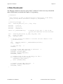
Application Examples ....................................................................................................... 6-1
Two-Channel Input Using On-Chip DMA .................................................................... 6-1
One- or Two-Channel Output Using Interrupts ............................................................ 6-2
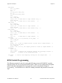
RTSI Switch Programming ........................................................................................... 6-4
A Data Downloader ....................................................................................................... 6-6
A Data Uploader ............................................................................................................ 6-7
An Audio Equalizer ....................................................................................................... 6-8
© National Instruments Corporation
xi
AT-DSP2200 User Manual
Contents
Appendix A
Specifications ........................................................................................................................A-1
DSP Engine ................................................................................................................... A-1
Memory ......................................................................................................................... A-1
DMA Controller ............................................................................................................ A-1
Interrupt Support ........................................................................................................... A-1
RTSI Bus Signals .......................................................................................................... A-2
Analog Input .................................................................................................................. A-2
Analog Output ............................................................................................................... A-3
Digital Trigger ............................................................................................................... A-4
Power Requirement (from PC AT I/O Channel) ........................................................... A-4
Physical Characteristics ................................................................................................. A-4
Operating Environment ................................................................................................. A-4
Storage Environment ..................................................................................................... A-4
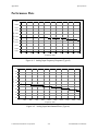
Performance Plots.......................................................................................................... A-5
Appendix B
Connectors ............................................................................................................................ B-1
Appendix C
Customer Communication .............................................................................................. C-1
Index .................................................................................................................................. Index-1
AT-DSP2200 User Manual
xii
© National Instruments Corporation
Contents
Figures
Figure 1-1. AT-DSP2200 Board ............................................................................................. 1-3
Figure
Figure
Figure
Figure
Figure
Figure
2-1.
2-2.
2-3.
2-4.
2-5.
2-6.
AT-DSP2200 Parts Locator Diagram................................................................... 2-2
Example Base I/O Address Switch Settings......................................................... 2-4
AC-Coupled Output Jumper Configuration ......................................................... 2-6
DC-Coupled Output Jumper Configuration ......................................................... 2-6
AT-DSP2200 I/O Connector Signal Assignments ............................................... 2-8
Timing Requirements for the EXTTRIG* Signal ................................................ 2-10
Figure
Figure
Figure
Figure
Figure
Figure
Figure
Figure
Figure
3-1.
3-2.
3-3.
3-4.
3-5.
3-6.
3-7.
3-8.
3-9.
AT-DSP2200 Block Diagram .............................................................................. 3-1
PC I/O Channel Interface Circuitry Block Diagram ............................................ 3-2
Analog Input Channel Block Diagram ................................................................. 3-4
Input Frequency Response ................................................................................... 3-7
Input Frequency Response Near the Cutoff ......................................................... 3-8
Comparison of a Clipped Signal to a Proper Signal ............................................. 3-10
Analog Output Channel Block Diagram .............................................................. 3-11
Signal Spectra ....................................................................................................... 3-13
RTSI Bus Interface Circuitry Block Diagram ...................................................... 3-16
Figure 4-1. RTSI Switch Control Pattern ................................................................................ 4-61
Figure 5-1. Calibration Trimpot Location Diagram ................................................................ 5-2
Figure 6-1. Audio Equalizer Function Panel........................................................................... 6-8
Figure A-1. Analog Input Frequency Response (Typical) ....................................................... A-5
Figure A-2. Analog Input Interchannel Phase (Typical).......................................................... A-5
Figure B-1. AT-DSP2200 I/O Connector Signal Assignments ............................................... B-1
Figure B-2. AT-DSP2200 RTSI Connector Signal Assignments ............................................ B-2
Tables
Table 2-1. Default Settings of National Instruments Products for the PC ............................. 2-3
Table 2-2. Switch Settings with Corresponding Base I/O Address and Base I/O
Address Space ...................................................................................................... 2-5
Table 2-3. I/O Connector Signal Descriptions....................................................................... 2-8
Table 3-1. AT-DSP2200 Sample Rates ................................................................................. 3-5
Table 3-2. AT-DSP2200 Alias Rejection at the Oversample Rate ........................................ 3-9
Table 3-3. AT-DSP2200 Update Rates.................................................................................. 3-9
Table 4-1. AT-DSP2200 I/O Channel Register Map ............................................................. 4-1
Table 4-2. AT-DSP2200 DSP Register Map ......................................................................... 4-19
Table 4-3. RTSI Trigger Lines .............................................................................................. 4-60
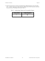
Table 5-1. Analog Input Channels and Corresponding Trimpots .......................................... 5-4
Table 5-2. Analog Output Channels and Corresponding Trimpots ....................................... 5-5
© National Instruments Corporation
xiii
AT-DSP2200 User Manual
Chapter 1
Introduction
This chapter describes the AT-DSP2200; lists the contents of your AT-DSP2200 kit; describes
the optional software and optional equipment; and explains how to unpack the AT-DSP2200.
The AT-DSP2200 is a high-accuracy, audio frequency, A/D, D/A, and DSP plug-in board for the
PC AT. The AT-DSP2200 uses the AT&T WE DSP32C DSP chip as the main computation
engine. With the WE DSP32C chip, the DSP application has 25 MFLOPS of processing power.
Many test and measurement applications can run in real time. Using the computational power of
the AT-DSP2200, you can perform real-time filtering and spectral analysis, which was
previously possible only with expensive stand-alone instruments. Process control applications
can also benefit from the AT-DSP2200 because you can use the computational power of the
AT-DSP2200 to develop complex process control algorithms on the PC.
Ultra-fast numeric computation power makes the AT-DSP2200 ideal for array processing
applications. The AT-DSP2200 has unique versatility and real-time performance capabilities,
which can be used in the following applications:
• General-purpose DSP
•
Instrumentation
•
Control
•
Medical research
•
Audio test and measurement
•
Graphics/imaging
•
Voice and speech analysis
•
Telecommunications
•
Industrial
•
Spectral analysis
The DSP section of the AT-DSP2200 has the following features:
• WE DSP32C single-chip digital signal processor
-
Operates at 50-MHz clock speed
-
25 MFLOPS/12.5 MIPS
-
32-bit instructions/24-bit addresses
© National Instruments Corporation
1-1
AT-DSP2200 User Manual
Introduction
•
•
•
Chapter 1
-
Two-operand and three-operand instructions
-
Parallel multiplier and arithmetic logic unit (ALU) instructions in a single cycle
-
Zero-overhead looping
-
32-bit floating-point precision/16-bit and 24-bit integer precision
-
Four 40-bit accumulators
-
Converts to or from IEEE-754 floating-point format in a single instruction
-
25 Mbits/sec serial I/O ports with interrupt or DMA to local memory options
-
16-bit parallel I/O port with interrupt or DMA to local memory options
-
Low-power CMOS technology
High-speed local memory
-
64, 128, 256, or 384 Kwords (1 word is 32 bits) of zero-wait-state onboard memory
-
1.5 Kwords of on-chip memory
-
Memory can be addressed as 8, 16, or 32 bits
Interrupt support
-
Interrupts from the AT-DSP2200 to the main CPU
-
Interrupts from the main CPU to the WE DSP32C chip
PC AT DMA
-
AT-DSP2200 memory to or from PC memory
-
AT-DSP2200 memory to or from an I/O board
The AT-DSP2200 has two channels of 16-bit, simultaneously sampled analog input with
64-times oversampling delta-sigma modulating A/D converters (ADC) and digital antialiasing
filters for extremely high-accuracy data acquisition. The two-channel output uses 8-times
oversampling digital anti-imaging filters and 64-times oversampling delta-sigma modulators.
Both input and output converters can run at conversion rates of up to 51.2 kHz.
The AT-DSP2200 can interface to the National Instruments Real-Time System Integration
(RTSI) bus, which includes a serial data link directly to and from other National Instruments AT
Series boards, such as the AT-A2150 four-channel dynamic signal acquisition board. With the
RTSI bus, sampling-clock synchronization is possible between multiple AT-DSP2200 boards for
simultaneous sampling on more than two channels. Also, the AT-DSP2200 can receive an
external interrupt request over the RTSI bus, that is normally used as a trigger signal, but can
also be used as a general-purpose, edge-triggered external interrupt.
AT-DSP2200 User Manual
1-2
© National Instruments Corporation
Chapter 1
Introduction
The AT-DSP2200 is useful for digitizing or synthesizing signals with bandwidths of 22 kHz or
less. The antialiasing filters on the input and the anti-imaging filters on the output ensure that
signals are acquired and reproduced with extremely high accuracy. Applications include audio
signal processing and analysis, audio workstations, audio and music synthesis, acoustics and
speech research, sonar, and audio frequency test and measurement.
The AT-DSP2200, which is designed for full audio-band measurements and signal analysis, is
equipped with crystal oscillators for standard digital audio and signal processing frequencies.
For more information about these frequencies, see Table 3-1 in Chapter 3, Theory of Operation.
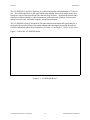
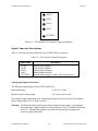
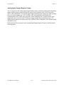
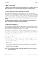
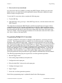
Figure 1-1 shows the AT-DSP2200 board.
Figure 1-1. AT-DSP2200 Board
© National Instruments Corporation
1-3
AT-DSP2200 User Manual
Introduction
Chapter 1
What Your Kit Should Contain
The contents of the AT-DSP2200 kit is listed as follows.
Kit Name and
Part Number
Kit Component
AT-DSP2200
64-Kword
version
(776597-01)
AT-DSP2200 board
AT-DSP2200 User Manual
NI-DSP software for DOS/LabWindows, with manual
NI-DSP software for LabVIEW for Windows, with manual
AT-DSP2200 Utilities and Examples diskette
5.25 in. diskette
3.5 in. diskette
NI-DAQ software for DOS/Windows/LabWindows, with manuals
181475-01
320435-01
776642-01
776752-01
AT-DSP2200
128-Kword
version
(776597-02)
AT-DSP2200
256-Kword
version
(776597-03)
AT-DSP2200
384-Kword
version
(776597-04)
Part Number
420234-83
422234-83
776250-01
420234-83
422234-83
776250-01
420234-83
422234-83
776250-01
420234-83
422234-83
776250-01
The part number of the AT-DSP2200 is printed on the component side of the board near the I/O
connector. This number identifies which version of the AT-DSP2200 board you have. Detailed
specifications for all versions of the AT-DSP2200 are included in Appendix A, Specifications, of
this manual.
If your kit is missing any of the components or if you received the wrong version, contact
National Instruments.
AT-DSP2200 User Manual
1-4
© National Instruments Corporation
Chapter 1
Introduction
This manual contains complete instructions for directly programming the AT-DSP2200. Your
AT-DSP2200 is packaged with NI-DSP for DOS/LabWindows, a high-level library of
ready-to-use DSP functions for the LabWindows developer or the QuickBASIC or C
programmer. The library consists of DSP functions, digital filtering functions, waveform
analysis functions, waveform generation functions, statistical analysis functions, vector and
matrix algebra functions, and numerical analysis functions.
The NI-DSP Interface Utilities are included in the NI-DSP for DOS/LabWindows software
package. You can use the NI-DSP Interface Utilities with the Developer Toolkit to customize
your NI-DSP library. A library of the object modules of each of the analysis functions in
NI-DSP is included, and you can link these modules with your custom functions using the
Developer Toolkit. The utility functions use the NI-DSP board device driver to handle data
communications, reset the DSP board, and download custom NI-DSP libraries. The utilities
package also contains tools for creating a library dispatcher and building a C interface to your
customized analysis functions.
In addition, your AT-DSP2200 is packaged with NI-DSP for LabVIEW for Windows, a library
of LabVIEW virtual instruments (VIs). The VI library consists of DSP functions for digital
filtering, waveform analysis, waveform generation, statistical analysis, vector and array
calculations, numerical analysis, and memory management.
Your AT-DSP2200 is also shipped with the NI-DAQ for DOS/Windows/LabWindows software.
NI-DAQ for DOS/Windows/LabWindows has a library of functions that can be called from your
application programming environment. These functions include routines for analog input (A/D
conversion), buffered data acquisition (high-speed A/D conversion), analog output (D/A
conversion), waveform generation, digital I/O, counter/timer, SCXI, RTSI, and self-calibration.
NI-DAQ for DOS/Windows/LabWindows maintains a consistent software interface among its
different versions so you can switch between platforms with minimal modifications to your code.
NI-DAQ for DOS/Windows/LabWindows comes with language interfaces for Professional
BASIC, Turbo Pascal, Turbo C, Turbo C++, Borland C++, and Microsoft C for DOS; and Visual
Basic, Turbo Pascal, Microsoft C with SDK, and Borland C++ for Windows. NI-DAQ for
DOS/Windows/LabWindows software is on high-density 5.25 in. and 3.5 in. diskettes.
Optional Software
You can use the AT-DSP2200 with LabVIEW for Windows or LabWindows for DOS.
LabVIEW and LabWindows are innovative program development software packages for data
acquisition and control applications. LabVIEW uses graphical programming, whereas
LabWindows enhances Microsoft C and QuickBASIC. Both packages include extensive
libraries for data acquisition, instrument control, data analysis, and graphical data presentation.
Part numbers for these software packages are listed in the following table.
Software
Part Number
LabVIEW for Windows
LabWindows
Standard package
Advanced Analysis Library
Standard package with the Advanced Analysis Library
776670-01
© National Instruments Corporation
1-5
776473-01
776474-01
776475-01
AT-DSP2200 User Manual
Introduction
Chapter 1
The Developer Toolkit (part number 776612-01) includes an AT&T WE DSP32C C compiler,
assembler, linker, simulator, and documentation. With these tools, you can directly program the
AT-DSP2200. You can take full advantage of the flexibility of the AT-DSP2200 to custom
tailor your DOS or LabWindows DSP system to your application. The C compiler generates
WE DSP32C assembly-language code that you can assemble and link into a run-time module.
After you have completed a run-time module, you use the download tools and/or the simulator to
load, simulate, and execute the code and display results.
Optional Equipment
Equipment
Part Number
Type RCA1 single cable
3 ft
6 ft
181341-03
181341-06
Type RCA2 dual cable
3 ft
6 ft
181342-03
181342-06
AT Series RTSI bus cables
Two boards
Three boards
Four boards
Five boards
776249-02
776249-03
776249-04
776249-05
Unpacking
Your AT-DSP2200 is shipped in an antistatic plastic package to prevent electrostatic damage to
the board. Several components on the board can be damaged by electrostatic discharge. To
avoid such damage in handling the board, take the following precautions:
•
Touch the plastic package to a metal part of your computer chassis before removing the
board from the package.
•
Remove the board from the package and inspect the board for loose components or any other
sign of damage. Notify National Instruments if the board appears damaged in any way. Do
not install a damaged board into your computer.
AT-DSP2200 User Manual
1-6
© National Instruments Corporation
Chapter 2
Configuration and Installation
This chapter explains board configuration, installation of the AT-DSP2200 in the PC, signal
connections to the board, and cabling considerations.
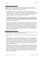
Board Configuration
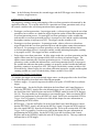
The AT-DSP2200 contains two jumpers to configure the analog output of the board and one DIP
switch to configure the AT bus interface setting. The DIP switch and jumpers are shown in the
parts locator diagram in Figure 2-1. The DIP switch U85 is used to set the base I/O address and
jumpers W1 and W2 configure the two analog outputs.
AT Bus Interface
The AT-DSP2200 is configured at the factory to use a base I/O address of hex 140. This setting,
shown in Figure 2-2b is suitable for most systems. However, if your system has other hardware
at this base I/O address, change these settings on the AT-DSP2200 as described in the previous
section Base I/O Address Selection. Record your settings in the configuration form in
Appendix C, Customer Communication.
© National Instruments Corporation
2-1
AT-DSP2200 User Manual
Configuration and Installation
Chapter 2
Figure 2-1. AT-DSP2200 Parts Locator Diagram
AT-DSP2200 User Manual
2-2
© National Instruments Corporation
Chapter 2
Configuration and Installation
Base I/O Address Selection
The base I/O address for the AT-DSP2200 is determined by the switches at position U85, as
shown in Figure 2-1. The switches are set at the factory for the base I/O address hex 140. The
National Instruments software packages use the factory setting as the default base I/O address
value for the AT-DSP2200. The AT-DSP2200 uses the I/O address space hex 140 through 15F
with the factory setting.
Note: Verify that this space is not already used by other equipment installed in your computer.
If any equipment in your computer uses this base I/O address space, you must change the
base I/O address of either the AT-DSP2200 or the other device. If you change the
AT-DSP2200 base I/O address, make a corresponding change to any software packages
you use with the AT-DSP2200. Table 2-1 lists the default settings of other National
Instruments products for the PC AT. For more information about the I/O address of your
PC AT, refer to the technical reference manual for your computer.
Table 2-1. Default Settings of National Instruments Products for the PC
Board
AT-A2150
AT-AO-6/10
AT-DIO-32F
AT-DSP2200
AT-GPIB
AT-MIO-16
AT-MIO-16F-5
GPIB-PCII
GPIB-PCIIA
GPIB-PCIII
Lab-PC
PC-DIO-24
PC-LPM-16
PC-TIO-10
DMA Channel
Interrupt Level
Base I/O
Address
None*
Channel 5
Channels 5, 6
None*
Channel 5
Channels 6, 7
Channels 6, 7
Channel 1
Channel 1
Channel 1
Channel 3
None
None
None
None*
Lines 11, 12
Lines 11, 12
None*
Line 11
Line 10
Line 10
Line 7
Line 7
Line 7
Line 5
Line 5
Line 5
Line 5
120 hex
1C0 hex
240 hex
140 hex
2C0 hex
220 hex
220 hex
2B8 hex
2E1 hex
280 hex
260 hex
210 hex
260 hex
1A0 hex
* These settings are software configurable and are disabled at startup time.
© National Instruments Corporation
2-3
AT-DSP2200 User Manual
Configuration and Installation
Chapter 2
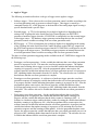
Each switch in U85 corresponds to one of the address lines A9 through A5. Press the side
marked OFF to select a binary value of 1 for the corresponding address bit. Press the other side
of the switch to select a binary value of 0 for the corresponding address bit. Figure 2-2 shows
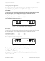
two possible switch settings.
1 2 3 4 5
This side down for 0
ON
This side down for 1
OFF
U85
a. Switches Set to Base I/O Address of Hex 000
A9 A8 A7 A6 A5
1 2 3 4 5
This side down for 0
ON
This side down for 1
OFF
U85
b. Switches Set to Base I/O Address of Hex 140 (Factory Setting)
(The shaded portion indicates the side of the switch that is pushed down.)
Figure 2-2. Example Base I/O Address Switch Settings
The AT-DSP2200 decodes the five least significant bits (LSBs) of the address, (A4 through A0),
to select the appropriate AT-DSP2200 register. To change the base I/O address, remove the
plastic cover on U85; press each switch to the desired position; verify that each switch is
completely pressed down; and if the plastic cover can be replaced, replace the plastic cover.
Make a note of the new AT-DSP2200 base I/O address for use when configuring the
AT-DSP2200 software on the configuration form in Appendix C, Customer Communication.
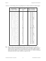
Table 2-2 lists the possible switch settings, the corresponding base I/O address, and the base I/O
address space used for that setting.
AT-DSP2200 User Manual
2-4
© National Instruments Corporation
Chapter 2
Configuration and Installation
Table 2-2. Switch Settings with Corresponding Base I/O Address and Base I/O Address Space
Switch Setting
A9 A8 A7 A6 A5
0
0
0
0
0
0
0
0
0
0
0
0
0
0
0
0
1
1
1
1
1
1
1
1
1
1
1
1
1
1
1
1
0
0
0
0
0
0
0
0
1
1
1
1
1
1
1
1
0
0
0
0
0
0
0
0
1
1
1
1
1
1
1
1
0
0
0
0
1
1
1
1
0
0
0
0
1
1
1
1
0
0
0
0
1
1
1
1
0
0
0
0
1
1
1
1
0
0
1
1
0
0
1
1
0
0
1
1
0
0
1
1
0
0
1
1
0
0
1
1
0
0
1
1
0
0
1
1
0
1
0
1
0
1
0
1
0
1
0
1
0
1
0
1
0
1
0
1
0
1
0
1
0
1
0
1
0
1
0
1
Base I/O Address
(hex)
000
020
040
060
080
0A0
0C0
0E0
100
120
140
160
180
1A0
1C0
1E0
200
220
240
260
280
2A0
2C0
2E0
300
320
340
360
380
3A0
3C0
3E0
Base I/O Address
Space Used (hex)
000 - 01F
020 - 03F
040 - 05F
060 - 07F
080 - 09F
0A0 - 0BF
0C0 - 0DF
0E0 - 0FF
100 - 11F
120 - 13F
140 - 15F
160 - 17F
180 - 19F
1A0 - 1BF
1C0 - 1DF
1E0 - 1FF
200 - 21F
220 - 23F
240 - 25F
260 - 27F
280 - 29F
2A0 - 2BF
2C0 - 2DF
2E0 - 2FF
300 - 31F
320 - 33F
340 - 35F
360 - 37F
380 - 39F
3A0 - 3BF
3C0 - 3DF
3E0 - 3FF
*
*
*
*
*
*
*
*
*
*
*
*
*
*
*
*
*
*
*
*
Note: Base I/O address values hex 000 through 0FF are reserved for system use. Base I/O
address values hex 100 through 3FF are available on the I/O channel. Addresses marked
with an asterisk (*) may be reserved, depending on the system, and should be avoided.
Please refer to the IBM Personal Computer AT Technical Reference manual for additional
information about the I/O space available to expansion cards.
© National Instruments Corporation
2-5
AT-DSP2200 User Manual
Configuration and Installation
Chapter 2
Analog Output Configuration
Two coupling options can be used for the analog outputs, AC and DC. Jumper W1 controls
output Channel 0 coupling and W2 controls output Channel 1 coupling.
AC Coupling
You can select the AC-coupled output configuration for either analog output channel by setting
the following jumpers. The two channels do not need to be configured the same way.
Analog Output Channel 0
W1
B-C
Analog Output Channel 1
W2
B-C
These configurations are shown in Figure 2-3.
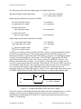
W2
W1
A B C
Channel 0
A B C
Channel 1
Figure 2-3. AC-Coupled Output Jumper Configuration
DC Coupling
You can select the DC-coupled output configuration for either analog output channel by setting
the following jumpers. The two channels do not need to be configured the same way.
Analog Output Channel 0
W1
A-B
Analog Output Channel 1
W2
A-B
These configurations are shown in Figure 2-4.
•
W2
•
W1
A B C
Channel 0
A B C
Channel 1
Figure 2-4. DC-Coupled Output Jumper Configuration
The factory-default setting for each output channel is DC coupling.
Analog Input Configuration
Analog input channel coupling (AC or DC) is software programmable and is discussed in
Chapter 4, Programming.
AT-DSP2200 User Manual
2-6
© National Instruments Corporation
Chapter 2
Configuration and Installation
Installation
You can install the AT-DSP2200 in any available 16-bit expansion slot (AT style) in your
computer. However, to achieve best noise performance, you should leave as much room as
possible between the AT-DSP2200 and other boards and hardware. The AT-DSP2200 does not
work if installed in an 8-bit expansion slot (PC style). After you have made any necessary
changes, verified, and recorded the switch settings, you are ready to install the AT-DSP2200.
The following are general installation instructions, but consult the user manual or technical
reference manual of your PC for specific instructions and warnings.
1. Turn off your computer.
2. Remove the top cover or access port to the I/O channel.
3. Remove the expansion slot cover on the back panel of the computer.
4. Insert the AT-DSP2200 into a 16-bit slot. It may be a tight fit, but do not force the board into
place. Verify that there are no tall components on the circuit board of the computer that may
touch or be in the way of any part of the AT-DSP2200 board.
5. If you want to connect multiple AT Series boards to each other, attach a RTSI cable to the
RTSI connector.
6. Screw the mounting bracket of the AT-DSP2200 to the back panel rail of the computer.
7. Check the installation.
8. Replace the cover.
The AT-DSP2200 board is installed and ready for operation.
Signal Connections
This section contains specifications and connection instructions for the I/O signals on the
AT-DSP2200 I/O connector.
I/O Connector Description
Figure 2-5 shows the signal assignments for the AT-DSP2200 I/O connector. This connector is
located on the back panel of the AT-DSP2200 board and is accessible at the rear of the PC after
the board has been properly installed. The connector consists of five RCA-type phono jacks and
accepts standard RCA-type phono plugs.
Warning: Connections that exceed any of the maximum ratings of input or output signals on
the AT-DSP2200 can result in damage to the AT-DSP2200 board and to the PC,
including connections of any power signals to ground. The description of each
signal in this section includes information about maximum input or output ratings.
National Instruments is not liable for any damages resulting from incorrect signal
connections.
© National Instruments Corporation
2-7
AT-DSP2200 User Manual
Configuration and Installation
Chapter 2
ACH 0
ACH 1
DAC 0
DAC 1
EXTTRIG*
Figure 2-5. AT-DSP2200 I/O Connector Signal Assignments
Signal Connection Descriptions
Table 2-3 lists the signal descriptions for the AT-DSP2200 I/O connector.
Table 2-3. I/O Connector Signal Descriptions
Signal Name
ACH0
ACH1
DAC0
DAC1
EXTTRIG*
Description
Analog input Channel 0
Analog input Channel 1
Analog output Channel 0
Analog output Channel 1
External digital trigger to start a conversion sequence
Analog Input Signal Connections
The following ratings apply to inputs ACH0 and ACH1:
Input signal range
±2.828 V (2 Vrms)
Maximum input voltage rating
±20 V powered on or off
Exceeding the input signal range does not damage the input circuitry as long as the maximum
input voltage rating of ±20 V is not exceeded.
Warning: Exceeding the input signal range results in distorted input signals. Exceeding the
maximum input voltage rating may result in damage to the AT-DSP2200 board and
to the PC. National Instruments is not liable for any damages resulting from
incorrect signal connections.
AT-DSP2200 User Manual
2-8
© National Instruments Corporation
Chapter 2
Configuration and Installation
Cabling Considerations
When you are connecting signal sources to the AT-DSP2200, use high-quality coaxial or
twisted-pair cables with low resistance and thorough shielding whenever possible. Sources
should be floating, although this is not always possible. The analog grounds on the
AT-DSP2200 are internally connected to the ground of the computer, which in turn is connected
to earth ground through the chassis and power connections. If a signal source is also grounded,
then a large ground-loop is set up when the signal source is connected to the board. This
condition sometimes induces a large amount of unwanted noise in the signal (especially 60-Hz
noise) and should be avoided whenever possible. Some signal sources have provisions for
floating the output ground, which significantly reduces noise in the signal. The same advice
applies to devices that are connected to the output of the AT-DSP2200.
Analog Output Signal Connections
The following ratings apply to outputs DAC0 and DAC1:
Output signal range
±2.828 V (2 Vrms)
Minimum load impedance
2 kΩ
The AT-DSP2200 is designed to be connected to loads with an input impedance of 10 kΩ or
greater. However, the output circuitry on the AT-DSP2200 performs to specification down to
2-kΩ loads. Driving loads of less than 2 kΩ increases distortion, especially near full-scale levels.
Also, because of the 50-Ω output impedance of the board, the output levels are diminished. For
example, connecting a 2-kΩ load causes the output level to drop -0.21 dB from the no-load level.
Because the board has short-circuit protection, you can connect the output to any load, even
headphones; however, the resulting distortion may be unacceptable–especially at higher signal
levels. The AT-DSP2200 delivers about ±14 mA, so it can acceptably drive low-impedance
loads.
Cabling Considerations
When you are connecting AT-DSP2200 outputs to other devices, use high-quality coaxial or
twisted-pair shielded cables whenever possible. Also, the ground of the receiving device should
be floated whenever possible to reduce ground-loop noise on the signal.
Digital Signal Connections
The digital trigger line (EXTTRIG*) is bidirectional, which means it can be used both to input
and output a digital trigger signal. When the board is not driving EXTTRIG*, the line appears as
an input at the I/O connector. When the board is driving EXTTRIG*, the line appears as a TTL
output.
© National Instruments Corporation
2-9
AT-DSP2200 User Manual
Configuration and Installation
Chapter 2
The following specifications and ratings apply to the digital trigger line.
Absolute maximum voltage input rating
+5.75 V with respect to DGND
-0.5 V with respect to DGND
Digital input specifications (referenced to DGND):
VIH input logic high voltage
VIL input logic low voltage
2 V minimum
0.8 V maximum
IIH input current load,
logic high input voltage
10 µA maximum
IIL input current load,
logic low input voltage
-10 µA maximum
Digital output specifications (referenced to DGND):
VOH output logic high voltage
VOL output logic low voltage
2.4 V minimum
0.5 V maximum
IOH high-level output current
IOL low-level output current
-3.2 mA
24 mA
A software event initiates a data acquisition operation. However, you can program the software
to initiate the operation because of an interrupt generated by the EXTTRIG* signal, by an
interrupt generated by a signal coming from the RTSI bus, or by the level of the digitized signal
crossing a certain threshold with a certain slope. The EXTTRIG* signal and the HWTRIG*
signal coming from the RTSI switch can be used to generate the INTREQ2* interrupt. This
interrupt, described further in Chapter 4, Programming, is normally used as a trigger, but also
serves as a general-purpose hardware interrupt. Notice that the A/D converter (ADC) operates in
a Free-Running mode; therefore, the triggering actually controls storage of the conversion data.
You can program the hardware trigger signal that generates the external interrupt to be
rising-edge triggered or falling-edge triggered. Figure 2-6 shows the timing requirements for the
EXTTRIG* signal when used as the source of the interrupt as a falling-edge triggered signal.
tw
VIH
tw 50 nsec minimum
VIL
Figure 2-6. Timing Requirements for the EXTTRIG* Signal
Because the software controls the beginning and ending of the data acquisition process, you have
complete control and great flexibility as to how the process begins and ends. For more
information on programming the WE DSP32C to control a data acquisition operation, refer to
Chapter 4, Programming.
AT-DSP2200 User Manual
2-10
© National Instruments Corporation
Chapter 3
Theory of Operation
This chapter contains a functional overview of the AT-DSP2200 and explains the operation of
each functional unit of the AT-DSP2200.
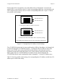
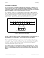
Functional Overview
The block diagram in Figure 3-1 is a functional overview of the AT-DSP2200.
RTSI Bus
RTSI
Switch
AT&T
WE DSP32C
Ext Ints
Interrupt
Register
PIO
Serial
Interface
∆-∑
A/D
LPF
AC/DC
Coupling
∆-∑
D/A
LPF
AC/DC
Coupling
Clock
Generation
and Selection
PIF
HW Trigger
External Trigger
Trigger
Control
Interrupt
Register
I/O Connector
Visual
Diagnostic
Register
Local
Memory
Interface
SIO
64k, 128k, 256k,
or 384k X 32
RAM
Control
and Status
Registers
Interrupt
Control
Circuitry
DMA
Control
Circuitry
AT Bus
Interface
PC AT I/O Channel
Figure 3-1. AT-DSP2200 Block Diagram;
The following are the major components of the AT-DSP2200 board:
•
PC I/O channel interface circuitry
•
DSP memory interface circuitry
•
Analog input circuitry
•
Analog output circuitry
© National Instruments Corporation
3-1
AT-DSP2200 User Manual
Theory of Operation
Chapter 3
•
Trigger circuitry
•
Real-Time System Integration (RTSI) bus interface circuitry
The internal data and control buses interconnect these components. The theory of operation of
each of these components is explained in the remainder of this chapter.
PC I/O Channel Interface Circuitry
The AT-DSP2200 board is a full-size, 16-bit, PC I/O channel adapter. The PC I/O channel
consists of a 24-bit address bus, a 16-bit data bus, a DMA arbitration bus, interrupt lines, and
several control and support signals. The components making up the AT-DSP2200 PC I/O
channel interface circuitry are shown in Figure 3-2.
Control and
Status
Registers
Bus
Transceivers
Address
Decoding
Circuitry
Control and
Status Signals
Register Selects
PC I/O Channel
Internal
Data Bus
PC I/O
Channel
Control
Circuitry
Interrupt
Control
Circuitry
Interrupt and
DMA Sources
DMA
Control
Circuitry
Figure 3-2. PC I/O Channel Interface Circuitry Block Diagram
AT-DSP2200 User Manual
3-2
© National Instruments Corporation
Chapter 3
Theory of Operation
Bus Transceivers
The bus transceivers control the sending and receiving of the data lines to and from the PC I/O
channel.
Address Decoder
The PC I/O channel has 24 address lines; the AT-DSP2200 uses 10 of these lines to decode the
board address. Therefore, the board address range is hex 000 to 3FF. You can use address lines
SA5 through SA9 to generate the board enable signal. The AT-DSP2200 uses SA0 through SA4
to select the onboard registers.
PC I/O Channel Control Circuitry
This circuitry monitors and transmits the PC I/O channel control and support signals. The
control signals identify transfers as read or write, memory or I/O, and 8-bit or 16-bit. The
AT-DSP2200 returns a support signal to the PC I/O channel to indicate the size of the current
data transfer.
Control and Status Registers
The AT-DSP2200 has several control and status registers. You can use two 16-bit control
registers, Interrupt/DMA Control and DMA TC Interrupt Clear, to program all of the interrupt
and DMA modes of the AT-DSP2200 and enable the DSP chip. The 16-bit Status Register
contains DMA and interrupt signal status information. You can use the nine other control and
status registers to communicate with the DSP chip through the DSP chip parallel port. Refer to
Chapter 4, Programming, for additional information about these registers.
Interrupt Control Circuitry
The interrupt control circuitry routes any enabled interrupts to the selected interrupt request lines.
The AT-DSP2200 can use one of eight interrupt request lines: IRQ3, IRQ4, IRQ5, IRQ9,
IRQ10, IRQ11, IRQ12, or IRQ15. With the interrupt requests, which are tri-state output signals,
the AT-DSP2200 board can share the interrupt lines with other devices. The AT-DSP2200
generates interrupts in the following situations:
•
When the PDR is full or empty, depending on the direction selected in the Interrupt/DMA
Control Register by the IN*/OUT bit
•
When the DSP chip sets an interrupt line
•
When a DMA TC pulse is received
Each one of these interrupts is individually enabled and cleared. See Chapter 4, Programming,
for additional information about programming with interrupts.
© National Instruments Corporation
3-3
AT-DSP2200 User Manual
Theory of Operation
Chapter 3
DMA Control Circuitry
You can assign the PDR a DMA channel for 16-bit data transfer. This channel has a DMA
enable bit, DMAEN. When DMA is enabled, the IN*/OUT bit is low (data is to be input to the
AT-DSP2200), the M/IO* bit is low (the AT-DSP2200 behaves as an I/O device for DMA), and
the PDR is empty, the AT-DSP2200 sends a DMA request. When DMA is enabled, the
IN*/OUT bit is high (data is to be output from the AT-DSP2200), the M/IO* bit is low (the
AT-DSP2200 behaves as an I/O device for DMA), and the PDR is full, the AT-DSP2200 sends a
DMA request. DMA Channels 5 through 7 of the PC I/O channel are available for such
transfers. If the AT-DSP2200 is running in an EISA computer, DMA Channels 0 through 3 are
also available as 16-bit DMA channels. If the M/IO* bit is high (the AT-DSP2200 behaves as a
memory device for DMA), the AT-DSP2200 does not generate DMA requests, but it responds to
DMA acknowledge cycles.
DSP Memory Interface Circuitry
The DSP memory interface connects the DSP chip to the onboard DSP memory, as well as to the
control and status registers that control and monitor the PC AT I/O channel interrupt circuitry,
the analog I/O circuitry, the RTSI bus interface circuitry, and the LEDs that indicate board status.
These registers are described in detail in Chapter 4, Programming.
Analog Input Circuitry
The AT-DSP2200 has two identical analog input channels. An analog input channel is illustrated
in Figure 3-3.
Analog
Signal
Input
Input Coupling
DC
AC
Gain Adjust
Analog Third-Order
Lowpass Filter
GND
16-Bit Data
64-Times
Decimating
Oversampling
Digital Filter
1-Bit Quantizer
ADC
Figure 3-3. Analog Input Channel Block Diagram
AT-DSP2200 User Manual
3-4
© National Instruments Corporation
Chapter 3
Theory of Operation
The AT-DSP2200 analog input circuitry simultaneously converts two bandlimited analog signals
to 16-bit two's complement digital signals. Both channels have an input range of ±2.828 V, or
2 Vrms full scale. Each of the input channels has input coupling selection, gain adjustment
circuitry, an analog antialiasing filter, a 64-times oversampling ADC, and a digital antialiasing
filter.
The AT-DSP2200, which is designed for full audio band measurements and signal processing
applications, is equipped with crystal oscillators for standard digital audio and digital signal
processing frequencies. The AT-DSP2200 has three oscillator crystals: X1, X2, and X3. A total
of 16 sample rates are derived from these crystals. X1 is divided by both 768 and 1,152,
producing two timebases. X2 and X3 are each divided by 384 to produce the other two timebases.
These timebases are the fastest sample rates on the board. Each of these timebases is divided by
2, 4, and 8 to produce 12 additional sample rates from which you can choose. The specific
sample rates available are listed in Table 3-1.
Table 3-1. AT-DSP2200 Sample Rates
X1
36.864 MHz
48 kHz
24 kHz
12 kHz
6 kHz
X2
16.9344 MHz
32 kHz
16 kHz
8 kHz
4 kHz
44.1 kHz
22.5 kHz
11.025 kHz
5.5125 kHz
X3
19.6608 MHz
51.2 kHz
25.6 kHz
12.8 kHz
6.4 kHz
Input Coupling
The AT-DSP2200 has a software-programmed switch that determines whether a capacitor is
placed in the signal path. If the switch is set for DC, the capacitor is bypassed, and any DC
offset present in the source signal being used is passed to the A/D converter (ADC). The DC
configuration is preferred because it places one less component in the signal path and thus has
higher fidelity. The DC configuration is recommended if the signal source has only small
amounts of offset voltage (less than ±25 mV) or if the source already has AC (capacitive)
coupling. If the source has a significant amount of unwanted offset (or bias voltage), however,
you must set the switch for AC coupling to take full advantage of the ±2.828 V input signal
range. Using AC coupling results in a drop in the low-frequency response of the analog input.
The -3 dB cutoff frequency is approximately 8.8 Hz, but the -0.01 dB cutoff frequency, for
instance, is considerably higher at approximately 180 Hz. Using AC coupling also results in a
total gain drop of about 0.009 dB from DC coupling. The input coupling switch also connects
the input circuitry to ground instead of to the signal source. This connection is usually made
during offset calibration, which is described in Chapter 4, Programming, and Chapter 5,
Calibration Procedures.
© National Instruments Corporation
3-5
AT-DSP2200 User Manual
Theory of Operation
Chapter 3
Calibration
The AT-DSP2200 analog inputs have calibration adjustments. The offset for each channel is
digitally nulled (calibrated to zero). You calibrate the gain for each channel by adjusting a
trimpot at the top of the circuit board. This trimpot has an approximately ±3.5% (±0.3 dB) gain
adjustment range for each channel. For complete calibration instructions, refer to Chapter 5,
Calibration Procedures.
Antialias Filtering
A sampling system (such as an ADC) can represent only signals of limited bandwidth.
Specifically, a sampler sampling at rate F s can represent only signals with a maximum frequency
of F s/2. This maximum frequency is known as the Nyquist frequency. If a signal is input to the
sampling system with frequency components that exceed the Nyquist frequency, then the
sampler cannot distinguish parts of this signal from some signals with frequency components less
than the Nyquist frequency.
For example, suppose a sampler (such as an ADC) is sampling at 1,000 Hz. If a 400-Hz sine
wave is input, then the resulting samples accurately represent a 400-Hz sine wave. However, if a
600-Hz sine wave is input, then the resulting samples again represent a 400-Hz sine wave (but
inaccurately) because this signal exceeds the Nyquist frequency (500 Hz) by 100 Hz. In fact, any
sine wave with a frequency greater than 500 Hz that is input is represented incorrectly as a signal
between 0 Hz and 500 Hz. The apparent frequency of this sine wave is the absolute value of the
difference between the frequency of the input signal and the closest integer multiple of
1,000 Hz (the sampling rate). Therefore, if a 2,325-Hz sine wave is input, its apparent frequency
is:
2,325 - (2)(1,000) = 325 Hz.
If a 3,975-Hz sine wave is input, its apparent frequency is:
(4)(1,000) - 3,975 = 25 Hz.
The process by which these higher frequency signals are modulated by the sampler back into the
0-Hz to 500-Hz baseband is called aliasing.
If the signal in the previous example is not a sine wave, the signal may have many components
(harmonics) that lie above the Nyquist frequency. If present, these harmonics are erroneously
aliased back into the baseband and added to the parts of the signal that are sampled accurately,
producing a distorted sampled data set. Only those signals that can be accurately represented
should be input to the sampler. All frequency components of such signals lie below the Nyquist
frequency. To make sure that only those signals go into the sampler, a lowpass filter is applied
to signals before they reach the sampler. The AT-DSP2200 has complete antialiasing filters.
The AT-DSP2200 includes two stages of antialias filtering in each input channel–an analog filter
and a digital filter. The analog filter is a third-order lowpass Butterworth filter. This filter has a
cutoff frequency of 80 kHz and a rejection of greater than 90 dB at 3 MHz. Because its cutoff
frequency is significantly higher than the data sample rate, the analog filter has an extremely flat
frequency response in the bandwidth of interest, and it has very little phase error.
AT-DSP2200 User Manual
3-6
© National Instruments Corporation
Chapter 3
Theory of Operation
The analog filter precedes the analog sampler, which operates at 64 times the selected sample
rate (3.072 MHz in the case of a 48-kHz sample rate) and is actually a 1-bit ADC. The 1-bit,
64-times oversampled data produced by the analog sampler is passed on to a digital antialiasing
filter that is built into the ADC chip. This filter also has extremely flat frequency response and
no phase error, but its cutoff frequency (about 0.45 times the sample rate) is extremely sharp, so
the rejection at and above the Nyquist frequency (0.5 times the sample rate) is greater than
85 dB. The output stage of the digital filter resamples the higher frequency data stream at the
output data rate, producing 16-bit digital samples.
With the AT-DSP2200 filters, you have the complete antialiasing protection needed to sample
signals accurately. The digital filter in each channel passes only those signal components with
frequencies that lie below the Nyquist frequency or within one Nyquist bandwidth of multiples
of 64 times the sample rate. The analog filter in each channel rejects possible aliases (mostly
noise) from signals that lie near these multiples. The frequency response of the AT-DSP2200
input circuitry is shown in Figure 3-4 and Figure 3-5.
-0
-10
-20
Amplitude (dB) -->
-30
-40
-50
-60
-70
-80
-90
-100
0.00
0.10
0.20
0.30
0.40
0.50
0.60
0.70
0.80
0.90
1.00
Frequency / Sample Rate -->
Figure 3-4. Input Frequency Response
© National Instruments Corporation
3-7
AT-DSP2200 User Manual
-0
-1
Amplitude (dB) -->
-2
-3
-4
-5
-6
0.400
0.410
0.420
0.430
0.440
0.450
0.460
Frequency / Sample Rate -->
Figure 3-5. Input Frequency Response Near the Cutoff
Because the ADC samples at 64 times the data rate, frequency components above 32 times the
data rate can alias. The digital filter rejects most of the frequency range over which aliasing can
occur. However, the filter can do nothing about components that lie close to 64 times the data
rate, 128 times the data rate, and so on, because it cannot distinguish these components from
components in the baseband (0 Hz to the Nyquist frequency). If, for instance, the sample rate is
48 kHz and a signal component lies within 24 kHz of 64 * 48 kHz or 3.072 MHz, then this signal
is aliased into the passband region of the digital filter and is not attenuated. The purpose of the
analog filter is to remove these higher frequency components near multiples of the oversampling
rate before they get to the sampler and the digital filter. While the frequency response of the
digital filter scales in proportion to the sample rate, the frequency response of the analog filter
remains fixed. The response of the filter is optimized to produce the most high-frequency alias
rejection while having the flattest in-band frequency response. Because this filter is third order,
its rolloff is rather slow. This means that although the filter has good alias rejection for high
sample rates, it does not reject as well at lower sample rates. The data sample rates, oversample
rates, and analog filter rejection at the oversample rates are tabulated in Table 3-2. The
rejections listed in this table apply only near the oversample frequency for the given sample rate.
For frequencies not near multiples of the oversample rate, the rejection is better than -85 dB.
© National Instruments Corporation
3-8
AT-DSP2200 User Manual
Chapter 3
Theory of Operation
Table 3-2. AT-DSP2200 Alias Rejection at the Oversample Rate
Data Sample Rate
51.2 kHz
48 kHz
44.1 kHz
32 kHz
25.6 kHz
24 kHz
22.05 kHz
16 kHz
12.8 kHz
12 kHz
11.025 kHz
8 kHz
6.4 kHz
6 kHz
5.5125 kHz
4 kHz
Oversample Rate
Alias Rejection
3.2768 MHz
3.072 MHz
2.8224 MHz
2.048 MHz
1.6384 MHz
1.536 MHz
1.4112 MHz
1.024 MHz
0.8192 MHz
0.768 MHz
0.7056 MHz
0.512 MHz
0.4096 MHz
0.384 MHz
0.3528 MHz
0.256 MHz
-97 dB
-95 dB
-93 dB
-84 dB
-79 dB
-77 dB
-75 dB
-66 dB
-60 dB
-59 dB
-57 dB
-48 dB
-42 dB
-41 dB
-39 dB
-30 dB
There is a form of aliasing that no filter can prevent. When a waveform exceeds the range of the
ADC, it is said to be clipped. When clipping occurs, the ADC assumes the closest value in its
digital range to the actual value of the signal, which is always either -32,768 or +32,767.
Clipping nearly always results in an abrupt change in the slope of the signal and causes the
corrupted digital data to have high-frequency energy. This energy is spread all through the
frequency spectrum, and because the clipping happens after the antialiasing filters, the energy is
aliased back into the baseband. The remedy for this problem is simple: do not allow the signal
to exceed the 2 Vrms range. Figure 3-6 shows the spectra of 2.1 Vrms and 2.0 Vrms, 2.962-kHz
sine waves digitized at 48 kHz. The signal-to-THD plus noise ratio is 35 dB for the clipped
waveform and 92 dB for the properly ranged waveform. Notice that aliases of all the harmonics
due to clipping appear in Figure 3-6a.
0
0
-20
-20
-40
-40
-60
-60
-80
-80
-100
-100
-120
-120
-140
-140
0
5000
10000
15000
20000
25000
0
a. Clipped Signal
5000
10000
15000
20000
25000
b. Proper Signal
Figure 3-6. Comparison of a Clipped Signal to a Proper Signal
© National Instruments Corporation
3-9
AT-DSP2200 User Manual
The ADC
The AT-DSP2200 ADCs use a method of A/D conversion known as delta-sigma modulation. If
the data rate is 48 kHz, each ADC actually samples its input signal at 3 MHz (64 times the data
rate) and produces 1-bit samples that are applied to the digital filter. This filter then expands the
data to 16 bits, rejects signal components greater than 24 kHz (the Nyquist frequency), and
resamples the data at the more conventional rate of 48 kHz. Although a 1-bit quantizer
introduces a large amount of quantization error to the signal, the 1-bit, 3-MHz samples from the
ADC carry all the information used to produce 16-bit samples at 48 kHz. The delta-sigma ADC
achieves this conversion from high speed to high resolution by adding a large amount of random
noise to the signal so that the resulting quantization noise, although large, is restricted to
frequencies above 24 kHz. This noise is uncorrelated with the input signal and is almost
completely rejected by the digital filter. The resulting output of the filter is a band-limited signal
with a dynamic range of over 93 dB. One of the advantages of a delta-sigma ADC is that it uses
a 1-bit D/A converter (DAC) as an internal reference, whereas most 16-bit ADCs use 16-bit
resistor-network DACs or capacitor-network DACs. As a result, the delta-sigma ADC is free
from the kind of differential nonlinearity (DNL) that is inherent in most high-resolution ADCs.
This lack of DNL is especially beneficial when the ADC is converting low-level signals, in
which noise and distortion are directly affected by converter DNL.
Noise
The AT-DSP2200 analog inputs typically have a 93 dB dynamic range. The dynamic range of a
circuit is the ratio of the magnitudes of the largest signal the circuit can carry and the residual
noise in the absence of a signal. In a 16-bit system, the largest signal is taken to be a full-scale
sine wave that peaks at the codes +32,767 and -32,768. Such a sine wave has a rms magnitude
of 32,768 / 1.414 = 23,170.475 least significant bits (LSBs). A grounded channel of the
AT-DSP2200 has noise level of about 0.5 LSB rms (this amount fluctuates). The ratio of
23,170.475 / 0.5 is about 46,341, or 93.3 dB, the dynamic range. Several factors can degrade the
noise performance of the inputs. First, noise can be picked up from nearby electronics. The
AT-DSP2200 works best when it is kept as far away as possible from other plug-in boards,
power supplies, disk drives, and computer monitors. There are also sources of interference on
the AT-DSP2200 itself. AT bus activity and DSP chip activity, although unavoidable, sometimes
causes small amounts of interference. Altering the pattern of activity may change the nature of
the interference. It is also possible for the conversion clock for the DAC to interfere with the
ADC if the DAC is being clocked at a rate different from that of the ADC. You should run both
the DAC and the ADC at the same rate whenever possible, even if you are not using the DAC.
Coding
The ADCs on the AT-DSP2200 produce two's complement 16-bit binary data. When 0 V is input,
the ADC returns the code 0000 hex, plus or minus some noise. 0 V corresponds to 0000 hex (0),
+2.828 V corresponds to 7FFF hex (+32,767), and -2.828 V corresponds to 8000 hex (-32,768).
The full-scale range of the input circuitry is 2 Vrms (5.657 V peak to peak).
Data Transfer
The AT-DSP2200 uses the serial data input port of the DSP chip for obtaining the A/D
conversion data. The data from both analog input channels is packed into one 32-bit word in the
serial port. The high-order 16-bits is Channel 0, and the low-order 16-bits is Channel 1.
© National Instruments Corporation
3-10
AT-DSP2200 User Manual
Chapter 3
Theory of Operation
The serial port on the DSP chip has a status signal that the DSP chip can poll. The status signal
can also generate a DSP interrupt, or generate a DSP DMA request whenever there is data in the
port to be read. For more information on the serial input port on the DSP chip, refer to the
WE DSP32C Digital Signal Processor Information Manual.
The AT-DSP2200 can also serially receive A/D conversion data over the RTSI bus from other
National Instruments boards, such as the AT-A2150 four-channel dynamic signal acquisition
board, for further processing. Data transfer over the RTSI bus is completely independent of the
AT bus. For more information on using the serial data links over the RTSI bus, refer to
Chapter 4, Programming.
Analog Output Circuitry
The AT-DSP2200 has two analog output channels, either of which is illustrated in Figure 3-7.
8-Times
Oversampling
Interpolating
Digital Filter
16-Bit
Data
64-Times
Oversampling
Digital Delta-Sigma
D/A Converter
Analog Lowpass
Filter
Gain Adjust
Coupling
AC
+
–
DC
Analog
Output
Signal
Figure 3-7. Analog Output Channel Block Diagram
The analog output circuitry simultaneously converts two 16-bit two's complement digital data
streams into band-limited analog signals. Both channels have an output range of ±2.828 V, or
2 Vrms. The available data conversion rates are listed in Table 3-3 (refer to the discussion of
timebases discussed previously in the section titled Analog Input Circuitry). Each channel has
digital and analog anti-imaging filters, gain adjustment circuitry, and a jumper to select AC or
DC coupling.
© National Instruments Corporation
3-11
AT-DSP2200 User Manual
Theory of Operation
Chapter 3
Table 3-3. AT-DSP2200 Update Rates
X1
36.864 MHz
48 kHz
24 kHz
12 kHz
6 kHz
X2
16.9344 MHz
32 kHz
16 kHz
8 kHz
4 kHz
44.1 kHz
22.5 kHz
11.025 kHz
5.5125 kHz
X3
19.6608 MHz
51.2 kHz
25.6 kHz
12.8 kHz
6.4 kHz
Anti-Image Filtering
A sampled signal repeats itself throughout the frequency spectrum. These repetitions begin
above one-half the sample rate (F s) and, at least in theory, continue up through the spectrum to
infinity, as shown in Figure 3-8a. Because the sample data actually represents only the
frequency components below one-half the sample rate (the baseband), it is desirable to filter out
all these extra images of the signal. In the AT-DSP2200, this filtering is accomplished in two
stages. First, the data is digitally resampled at eight times the original sample rate. Then, a
linear-phase digital filter removes almost all energy above one-half the original sample rate and
sends the data at the eight-times rate to the DAC, as shown in Figure 3-8b. Some further
(inherent) filtering occurs at the DAC because the data is digitally sampled and held at eight
times the sample rate. This filtering has a "sin x / x" response, yielding nulls at multiples of eight
times the sample rate, as shown in Figure 3-8c. Still, images remain, and they must be filtered
out. Each output channel of the AT-DSP2200 has discrete-time (switched-capacitor) and
continuous-time analog filters that remove the high-frequency images, as shown in Figure 3-8d.
AT-DSP2200 User Manual
3-12
© National Instruments Corporation
Chapter 3
Theory of Operation
Images
Amplitude
Baseband Signal
Fs
8Fs
16Fs
Frequency
16Fs
Frequency
16Fs
Frequency
16Fs
Frequency
a. Spectrum of Sampled Signal
Images After the Digital Filter
Amplitude
Baseband Signal
Fs
8Fs
b. Spectrum of Signal After Digital Filter
Images After the DAC
Amplitude
Baseband Signal
Fs
8Fs
c. Spectrum of Signal After DAC
Amplitude
Baseband Signal
Fs
8Fs
d. Spectrum of Signal After Analog Filters
Figure 3-8. Signal Spectra in the DAC
© National Instruments Corporation
3-13
AT-DSP2200 User Manual
Theory of Operation
Chapter 3
The DAC
The 64-times oversampling delta-sigma DACs on the AT-DSP2200 work in the same way as
delta-sigma ADCs, only in reverse. The digital data first passes through a digital lowpass filter
and then goes to the delta-sigma modulator. In the ADC the delta-sigma modulator is analog
circuitry that converts high-resolution analog signals to high-rate 1-bit digital data, whereas in
the DAC the delta-sigma modulator is digital circuitry that converts high-resolution digital data
to high-rate 1-bit digital data. As in the ADC, the modulator frequency-shapes the quantization
noise so that almost all of its energy is above the signal frequency (refer to the section titled The
ADC, earlier in this chapter). The digital 1-bit data is then sent directly to a simple 1-bit DAC.
This DAC can have only one of two analog values, and so is inherently perfectly linear. The
output of the DAC, however, has a large amount of quantization noise at higher frequencies, and,
as described in the previous section titled Anti-Image Filtering, some images still remain near
multiples of eight times the sample rate. Two analog filters eliminate the quantization noise and
the images. The first is a fifth-order, switched-capacitor filter in which the cutoff frequency
scales with the sample frequency and is approximately 0.52 times the sample frequency. This
filter has a four-pole Butterworth response and an extra pole at about 1.04 times the sample
frequency. The second filter is a continuous-time, second-order Butterworth filter in which the
cutoff frequency (at 80 kHz) does not scale with the sample frequency. This filter mainly
removes high-frequency images from the 64-times oversampled switched-capacitor filter.
Calibration
The AT-DSP2200 analog outputs have calibration adjustments. The offset for each channel is
nulled (calibrated to zero) digitally to within ±3 mV. The gain for each channel is calibrated by
adjusting a trimpot at the top of the circuit board. This trimpot has an approximately ±6%
(±0.5 dB) gain adjustment range for each channel. For complete calibration instructions, refer to
Chapter 5, Calibration Procedures.
Mute Feature
The two-channel DAC chip on the AT-DSP2200 goes into mute mode if the chip receives at least
4,096 consecutive zero values on both channels at once. In mute mode, the outputs are clamped
to ground and the noise floor drops from about 92 dB below full-scale to about 120 dB below
full-scale. Upon receiving any nonzero data, the DAC instantly reverts to normal mode. Mute
mode is designed to quiet the background noise to extremely low levels when no waveforms are
being generated. Mute mode does, however, have a slightly different offset from the normal
offset when zeros are being sent. As a result, the DAC has one offset for the first 4,096 zero
samples and then another offset in mute mode for as long as zeros are sent. This difference is
usually less than 1 mV.
Output Coupling
Following the analog filter, the AT-DSP2200 has a jumper that selects either AC or DC output
coupling. Some inputs of devices to which the AT-DSP2200 can be connected require AC
coupling, because DC coupling could disturb the DC biasing on the device. If AC coupling is
not required, then you should use DC coupling. Each output signal has a 51-Ω resistor in series.
This resistor protects the board from short circuits and helps stabilize the output circuitry when
driving large capacitive loads such as long cables.
AT-DSP2200 User Manual
3-14
© National Instruments Corporation
Chapter 3
Theory of Operation
Coding
The DACs on the AT-DSP2200 accept two's complement 16-bit binary data. The code 0000 hex
produces a 0 V (center-scale) output. The code 7FFF hex produces a +2.828 V (positive
full-scale) output. The code 8000 hex produces a -2.828 V (negative full-scale) output. Other
codes produce their proportional output voltages.
Data Transfer
The AT-DSP2200 uses the serial data output port of the DSP chip for supplying the D/A
conversion data. The data for both analog output channels is packed into one 32-bit word in the
serial port. The high-order 16-bits is Channel 0, and the low-order 16-bits is Channel 1.
The serial port on the DSP chip has a status signal that the DSP chip can poll. The status signal
can also generate a DSP interrupt, or generate a DSP DMA request whenever the port is ready to
be written. For more information on the serial output port on the DSP chip, refer to the
WE DSP32C Digital Signal Processor Information Manual.
The AT-DSP2200 can also serially send D/A conversion data over the RTSI bus to other
National Instruments boards. Data transfer over the RTSI bus is completely independent of the
AT bus. For more information on using the serial data links over the RTSI bus, refer to
Chapter 4, Programming.
Trigger Circuitry
You can trigger the AT-DSP2200 to start a data acquisition sequence from one of three possible
sources. These sources are listed as follows:
•
A software trigger
•
A TTL-level trigger from an external source applied at EXTTRIG* on the I/O connector
•
A trigger received over the RTSI bus from another AT Series board
In addition to these triggering capabilities, you can program the AT-DSP2200 to drive the
EXTTRIG* signal on the I/O connector with the trigger received over the RTSI bus.
RTSI Bus Interface Circuitry
The AT-DSP2200 is interfaced to the National Instruments RTSI bus. The RTSI bus has a clock
line, seven trigger lines, and four serial data links. You can wire together all National
Instruments AT Series data acquisition boards with RTSI bus connectors together inside the PC
to share these signals. A block diagram of the RTSI bus interface circuitry is shown in
Figure 3-9.
© National Instruments Corporation
3-15
AT-DSP2200 User Manual
Theory of Operation
Chapter 3
ADC Master
MClock
RTSI MClock
ADC Slave*
ADC Master
APD
RTSI APD (Trigger 6)
DAC Master
ETRIGDRV
EXTTRIG*
ETRIGRCV
DAC Slave*
RTSI SEL*
Internal Data Bus
HWTrig*
WCAD
WCDA
RTSITrig*
Reserved
Reserved
Reserved
/SEL
Data
RTSI
Switch
A0
A1
A2
A3
A4
A5
A6
B0
B1
B2
B3
B4
B5
B6
/
5
N/C
N/C
3
Serial In
Clocks & Data
ADC*/SL
SL1*/SL3
Trigger
/
7
3
Serial Link 1
3
Serial Link 3
/
/
/
MUX
RTSI Bus Connector
ADC Slave*
RTSI XI (Trigger 5)
XI
3 Onboard ADC
/
3 Serial Link 0
3
Serial Out
/
Clocks & Data
DAC*/SL
SL0*/SL2
/
3 Serial Link 2
/
DEMUX
3 Onboard DAC
/
Figure 3-9. RTSI Bus Interface Circuitry Block Diagram
Figure 3-9 shows the RTSI clock drivers, the RTSI switch, and the four serial links. These
drivers and the RTSI switch route AT-DSP2200 signals to and from the RTSI Bus.
The RTSI switch is a National Instruments custom-integrated circuit that acts as a 7x7 crossbar
switch. Pins B<4..0> are connected to the five RTSI bus trigger lines. The sixth line in the RTSI
bus trigger lines, B5 (Trigger 5), is used as a master clock so that multiple AT-DSP2200 boards
can update the DACs at the same rate. The seventh line in the RTSI bus trigger lines, B6
(Trigger 6), is used on the AT-DSP2200 in conjunction with another signal for multiple-board
sampling clock synchronization. Pins A<3..0> are connected to four signals on the board. Other
pins on the A side are reserved. The RTSI switch can drive any of the signals at pins A<6..0>
onto any one or more of the seven pins B<6..0> and can drive any of the signals present at the
seven pins B<6..0> onto any one or more of the pins A<6..0>. With this capability, a completely
flexible signal interconnection scheme is possible for any AT Series board sharing the RTSI bus.
The RTSI switch is programmed through select and data inputs.
AT-DSP2200 User Manual
3-16
© National Instruments Corporation
Chapter 3
Theory of Operation
On the AT-DSP2200 board, four signals are connected to pins A<3..0> of the RTSI switch. The
signal HWTrig* is the final hardware trigger used to generate an external interrupt to the WE
DSP32C for triggering a data acquisition operation and can originate from the EXTTRIG* signal
receiving circuitry or from the RTSI switch. The signal labeled WCAD is the A/D sampling
clock signal. The signal labeled WCDA is the D/A update clock signal. RTSITrig* is a signal
generated by the Analog Input/Output Control Register controlled by the WE DSP32C and is
used to test the hardware trigger functionality of the AT-DSP2200. RTSITrig* is also used to
send a common hardware trigger generated by a single software operation to multiple ATDSP2200 boards connected via the RTSI bus.
In addition to the RTSI switch, the AT-DSP2200 can use a serial data link to transmit or receive
data between the AT-DSP2200 and other AT Series boards sharing the RTSI bus, such as the
AT-A2150. For more information on the RTSI switch and the serial data link, refer to
Chapter 4, Programming.
© National Instruments Corporation
3-17
AT-DSP2200 User Manual
Chapter 4
Programming
This chapter discusses in detail how to program the AT-DSP2200 and describes the
AT-DSP2200 control and status registers. This chapter includes the AT-DSP2200 register
address map, a detailed description for each register, and a functional programming description.
Note:
If you plan to use a programming software package such as NI-DAQ, NI-DSP, or
LabWindows with your AT-DSP2200 board, you do not need to read this chapter.
Refer to your software documentation for programming information.
I/O Channel Register Map
The register map for the AT-DSP2200 as viewed from the PC is shown in Table 4-1. This table
gives the register name, the register address, the type of the register (read-only, write-only, or
read-and-write), and the size of the register in bits.
I/O Channel Register Sizes
Two different transfer sizes can be used for read and write operations with the PC: byte
(8-bit), and word (16-bit). Table 4-1 shows the size of each AT-DSP2200 register. For example,
reading or writing to the PAR Register requires a 16-bit (word) read-or-write operation at the
selected address, whereas reading or writing to the PARE Register requires an 8-bit (byte) reador-write operation at the selected address.
Table 4-1. AT-DSP2200 I/O Channel Register Map
Register Name
Address (Hex)
Type
DSP Register Group
PAR
PDR
EMR
ESR
PCRl
PIR
PCRh
PARE
PDR2
Base address + 00
Base address + 02
Base address + 04
Base address + 06
Base address + 07
Base address + 08
Base address + 0A
Base address + 0B
Base address + 0C
Read-and-write
Read-and-write
Read-and-write
Read-only
Read-and-write
Read-and-write
Read-and-write
Read-and-write
Read-and-write
16-bit
16-bit
16-bit
8-bit
8-bit
16-bit
8-bit
8-bit
16-bit
Interrupt/DMA Register Group
Interrupt/DMA Control Register
Status Register
Base address + 10
Base address + 10
Write-only
Read-only
16-bit
16-bit
© National Instruments Corporation
4-1
Size
AT-DSP2200 User Manual
Programming
DMA TC Interrupt Clear Register
AT-DSP2200 User Manual
Chapter 4
Base address + 12
4-2
Write-only
16-bit
© National Instruments Corporation
Chapter 4
Programming
I/O Channel Register Description
Table 4-1 divides the AT-DSP2200 registers into two register groups. A bit description of each
of the registers making up these groups is included later in this chapter.
The DSP Register Group is used to control and read and write data from the parallel port of the
WE DSP32C. The Interrupt/DMA Register Group is used to control and obtain the status of the
interrupt and/or DMA facility on the AT-DSP2200 board.
I/O Channel Register Description Format
The remainder of this register description section discusses each of the AT-DSP2200 registers in
the order shown in Table 4-1. Each register group is introduced, followed by a detailed bit
description of each register. The individual register description gives the address, type, word
size, and bit map of the register, followed by a description of each bit.
The register bit map shows a diagram of the register with the most significant bit (MSB) (bit 15
for a 16-bit register, bit 7 for an 8-bit register) shown on the left, and the least significant bit
(LSB) (bit 0) shown on the right. A rectangle is used to represent each bit. Each bit is labeled
with a name inside its rectangle. An asterisk (*) after the bit name indicates that the bit is
inverted (negative logic).
In many of the registers, the bits labeled with a 0 value indicate reserved bits. When a register is
written, these bits must be set to zero.
In many of the registers, several bits are labeled with an X, indicating don't care bits. When a
register is read, these bits may appear set or cleared but should be ignored because they have no
significance. When a register is written to, setting or clearing these bit locations has no effect on
the AT-DSP2200 hardware.
The bit map field for some write-only registers state not applicable, no bits used. Writing to one
of these registers causes some onboard event to occur, such as clearing the DMA TC circuitry.
The data is ignored when writing to these registers; therefore, any bit pattern is sufficient.
© National Instruments Corporation
4-2
AT-DSP2200 User Manual
Programming
Chapter 4
DSP Register Group
The DSP Register Group controls, reads, and writes data from the parallel port of the
WE DSP32C chip.
Bit descriptions for the registers in the DSP Register Group are detailed on the following pages.
For more information about the parallel port on the WE DSP32C chip, refer to the WE DSP32C
Digital Signal Processor Information Manual.
AT-DSP2200 User Manual
4-3
© National Instruments Corporation
Chapter 4
Programming
PIO Address Register (PAR)
The PAR is a 16-bit register that is loaded with the lower 16 bits of the on-chip DMA address.
Address:
Base address + 00 (hex)
Type:
Read-and-write
Word Size:
16-bit
Bit Map:
15
14
13
12
11
10
9
8
PAR15
PAR14
PAR13
PAR12
PAR11
PAR10
PAR9
PAR8
7
6
5
4
3
2
1
0
PAR7
PAR6
PAR5
PAR4
PAR3
PAR2
PAR1
PAR0
Bit
Name
Description
15-0
PAR<15..0>
These are the lower 16 bits of the on-chip DMA address. Bit 0 of
the PAR is not used and returns a logic one (1) when read. For
more information on the PAR, refer to the WE DSP32C Digital
Signal Processor Information Manual.
© National Instruments Corporation
4-4
AT-DSP2200 User Manual
Programming
Chapter 4
PIO Data Register (PDR)
The PDR is a 16-bit register that can be read or written by both the PC and the WE DSP32C
chip.
Address:
Base address + 02 (hex)
Type:
Read-and-write
Word Size:
16-bit
Bit Map:
15
14
13
12
11
10
9
8
PDR15
PDR14
PDR13
PDR12
PDR11
PDR10
PDR9
PDR8
7
6
5
4
3
2
1
0
PDR7
PDR6
PDR5
PDR4
PDR3
PDR2
PDR1
PDR0
Bit
Name
Description
15-0
PDR<15..0>
These are the 16 bits of data written or read by the PC or the WE
DSP32C. Writing to the PDR by the PC or the DSP chip sets the
PDF flag and the PDFs bit in the PCRl and reading the PDR clears
the PDF flag and the PDFs bit in the PCRl. The PDF flag can be
used to generate a PC interrupt or DMA request. The PDF flag can
also be used to generate two internal DSP interrupts, or the DSP
chip can poll for the status of this flag internally. The DSP chip
can use the PDR in conjunction with the PDR2 to perform
32-bit data transfers. If this is done, then the PDR is used for the
upper 16 bits and the PDR2 is used for the lower 16 bits. For more
information on the PDR, refer to the WE DSP32C Digital Signal
Processor Information Manual.
AT-DSP2200 User Manual
4-5
© National Instruments Corporation
Chapter 4
Programming
Error Mask Register (EMR)
The EMR is a 16-bit register that can be used to mask or unmask notification and halting the
DSP chip because of errors that occur in code being run by the DSP chip.
Address:
Base address + 04 (hex)
Type:
Read-and-write
Word Size:
16-bit
Bit Map:
15
14
13
12
11
10
9
8
HLOSY
HLOS
HADER
HOUE
1
1
HNAN
1
7
6
5
4
3
2
1
0
NLOSY
NLOS
NADER
NOUE
1
1
NNAN
1
Bit
Name
Description
15
HLOSY
Halt on Loss of Sync Error Mask – If this bit is set or the NLOSY
bit is set, mask the ESR LOSY bit from halting the DSP chip. If
this bit is cleared and the NLOSY bit is cleared, the LOSY bit
causes the DSP chip to be halted.
14
HLOS
Halt on Loss of Sanity Error Mask – If this bit is set or the NLOS
bit is set, mask the ESR LOS bit from halting the DSP chip. If this
bit is cleared and the NLOS bit is cleared, the LOS bit causes the
DSP chip to be halted.
13
HADER
Halt on Addressing Error Mask – If this bit is set or the NADER
bit is set, mask the ESR ADER bit from halting the DSP chip. If
this bit is cleared and the NADER bit is cleared, the ADER bit
causes the DSP chip to be halted.
12
HOUE
Halt on Overflow or Underflow Error Mask – If this bit is set or
the NOUE bit is set, mask the ESR OUE bit from halting the DSP
chip. If this bit is cleared and the NOUE bit is cleared, the OUE
bit causes the DSP chip to be halted.
11-10
1
Reserved bits – These bits must be set to one.
9
HNAN
Halt on Not a Number Error Mask – If this bit is set or the NNAN
bit is set, mask the ESR NAN bit from halting the DSP chip. If
this bit is cleared and the NNAN bit is cleared, the NAN bit causes
the DSP chip to be halted.
8
1
Reserved bit – This bit must be set to one.
© National Instruments Corporation
4-6
AT-DSP2200 User Manual
Programming
Chapter 4
Bit
Name
Description (Continued)
7
NLOSY
Notify on Loss of Sync Error Mask – If this bit is set, mask the
ESR LOSY bit from setting the PIF flag. If this bit is cleared, the
LOSY bit causes the PIF flag to be set.
6
NLOS
Notify on Loss of Sanity Error Mask – If this bit is set, mask the
ESR LOS bit from setting the PIF flag. If this bit is cleared, the
LOS bit causes the PIF flag to be set.
5
NADER
Notify on Addressing Error Mask – If this bit is set, mask the ESR
ADER bit from setting the PIF flag. If this bit is cleared, the
ADER bit causes the PIF flag to be set.
4
NOUE
Notify on Overflow or Underflow Error Mask – If this bit is set,
mask the ESR OUE bit from setting the PIF flag. If this bit is
cleared, the OUE bit causes the PIF flag to be set.
3-2
1
Reserved bits – These bits must be set to one.
1
NNAN
Notify on Not a Number Error Mask – If this bit is set, mask the
ESR NAN bit from setting the PIF flag. If this bit is cleared, the
NAN bit causes the PIF flag to be set.
0
1
Reserved bit – This bit must be set to one.
AT-DSP2200 User Manual
4-7
© National Instruments Corporation
Chapter 4
Programming
Error Source Register (ESR)
The ESR contains the status of several error conditions that may occur in the WE DSP32C chip.
The effect of receiving these error conditions is determined by the contents of the EMR. The
ESR is only readable by the PC and is cleared after being read. The ESR is cleared on reset of
the WE DSP32C chip.
Address:
Base address + 06 (hex)
Type:
Read-only
Word Size:
8-bit
Bit Map:
7
6
5
4
3
2
1
0
LOSY
LOS
ADER
OUE
0
WPIR
NAN
1
Bit
Name
Description
7
LOSY
Loss of Sync – If this bit is set, loss of external synchronization.
6
LOS
Loss of Sanity – If this bit is set, sanity in the IOC register is set
and SY changes state from high to low.
5
ADER
Addressing Error – If this bit is set, an attempt was made to access
a float variable on an address that was not a multiple of four or an
integer variable with an address that was not a multiple of two.
4
OUE
Overflow or Underflow Error – If this bit is set, DAU overflow or
underflow occurred.
3
0
Reserved bit – This bit always returns a zero.
2
WPIR
Write PIR – If this bit is set, the PIR was written.
1
NAN
Not a Number Error – If this bit is set, IEEE to WE DSP32C float
conversion detected a NAN.
0
1
Reserved bit – This bit always returns a one.
© National Instruments Corporation
4-8
AT-DSP2200 User Manual
Programming
Chapter 4
Parallel I/O Control Register Low (PCRl)
The PCRl controls and monitors the status of the parallel port of the WE DSP32C chip.
Address:
Base address + 07 (hex)
Type:
Read-and-write
Word Size:
8-bit
Bit Map:
7
6
5
4
3
2
1
0
0
PIFs
PDFs
AUTO
DMA
ENI
REGMAP
RESET
Bit
Name
Description
7
0
Reserved bit – This bit must be set to zero.
6
PIFs
PIR Status (read-only) – This bit is set when the PIR is written by
the WE DSP32C chip or by the PC. It is cleared when the PIR is
read by the WE DSP32C chip or by the PC.
5
PDFs
PDR Status (read-only) – This bit is set when the PDR is written
by the WE DSP32C chip or by the PC. It is cleared when the PDR
is read by the WE DSP32C chip or by the PC.
4
AUTO
Autoincrement – This is the on-chip parallel port DMA
autoincrement control bit. If this bit is low, the PAR and the
PARE are not autoincremented on parallel port DMA. If this bit is
high, then the PAR and the PARE are autoincremented on parallel
port DMA.
3
DMA
DMA – This is the on-chip parallel port DMA enable bit. If this
bit is low, PIO DMA is disabled. If this bit is high, PIO DMA is
enabled.
2
ENI
Enable PIF – This is the PIF enable bit. When this bit is low, the
PIF is not affected by reads and writes of the PIR. If this bit is
high, the PIF is enabled when the PIR is written, and cleared when
the PIR is read.
1
REGMAP
Register Map – This bit selects the register map used by the I/O
address decoding circuitry of the WE DSP32C chip. This bit
should be set high for normal operations of the AT-DSP2200.
0
RESET
Reset the WE DSP32C Chip – If this bit is cleared, the
WE DSP32C chip is halted. If this bit is high, the WE DSP32C
chip is in Run mode. A low-to-high transition of this bit initiates a
reset sequence of the WE DSP32C chip.
AT-DSP2200 User Manual
4-9
© National Instruments Corporation
Chapter 4
Programming
PIO Interrupt Register (PIR)
The PIR is a 16-bit register that can be read or written by both the PC and the WE DSP32C.
Address:
Base address + 08 (hex)
Type:
Read-and-write
Word Size:
16-bit
Bit Map:
15
14
13
12
11
10
9
8
PIR15
PIR14
PIR13
PIR12
PIR11
PIR10
PIR9
PIR8
7
6
5
4
3
2
1
0
PIR7
PIR6
PIR5
PIR4
PIR3
PIR2
PIR1
PIR0
Bit
Name
Description
15-0
PIR<15..0>
These are the 16 bits of data written or read by the PC or the
WE DSP32C chip. When the ENI bit in the PCRl is set, writing to
the PIR by the PC or the DSP chip sets the PIF flag and the PIFs
bit in the PCRl, and reading the PIR clears the PIF flag and the
PIFs bit in the PCRl. The PIF flag can be used to generate an
external DSP interrupt at INTRQ1*, or the DSP chip can poll for
the status of this flag internally. For more information on the PIR,
refer to the WE DSP32C Digital Signal Processor Information
Manual.
© National Instruments Corporation
4-10
AT-DSP2200 User Manual
Programming
Chapter 4
Parallel I/O Control Register High (PCRh)
The PCRh controls and monitors the status of the parallel port of the WE DSP32C chip.
Address:
Base address + 0A (hex)
Type:
Read-and-write
Word Size:
8-bit
Bit Map:
7
6
5
4
3
2
1
0
0
0
0
0
0
FLG
PIO16
DMA32
Bit
Name
Description
7-3
0
Reserved bits – These bits must be set to zero.
2
FLG
Flag – If this bit is low, the PDF and PIF flags change on the
leading edge of reads. If this bit is high, the PDF and PIF flags
change on the trailing edge of reads.
1
PIO16
This bit controls the size of the PIO interface. If this bit is low, the
PIO interface is eight bits. If this bit is high, the PIO interface is
16 bits. This bit should be set high for normal operation of the
AT-DSP2200 bus interface.
0
DMA32
This bit controls the size of the DMA transfers to and from the
onboard DSP memory. If this bit is low, the DMA transfers are 16
bits (using the PDR only). If this bit is high, the DMA transfers
are 32 bits (using both the PDR and PDR2).
AT-DSP2200 User Manual
4-11
© National Instruments Corporation
Chapter 4
Programming
PIO Address Register Extended (PARE)
The PARE is a 16-bit register that is loaded with the upper eight bits of the on-chip DMA
address.
Address:
Base address + 0B (hex)
Type:
Read-and-write
Word Size:
8-bit
Bit Map:
7
6
5
4
3
2
1
0
PARE7
PARE6
PARE5
PARE4
PARE3
PARE2
PARE1
PARE0
Bit
Name
Description
7-0
PARE<7..0>
These are the upper eight bits of the 24-bit address used as the
source or destination address of on-chip DMA transfers. For more
information on the PARE, refer to the WE DSP32C Digital Signal
Processor Information Manual.
© National Instruments Corporation
4-12
AT-DSP2200 User Manual
Programming
Chapter 4
PIO Data Register 2 (PDR2)
The PDR2 is a 16-bit register that can be read or written by both the PC and the WE DSP32C
chip.
Address:
Base address + 0C (hex)
Type:
Read-and-write
Word Size:
16-bit
Bit Map:
15
14
13
12
11
10
9
8
PDR2_15
PDR2_14
PDR2_13
PDR2_12
PDR2_11
PDR2_10
PDR2_9
PDR2_8
7
6
5
4
3
2
1
0
PDR2_7
PDR2_6
PDR2_5
PDR2_4
PDR2_3
PDR2_2
PDR2_1
PDR2_0
Bit
Name
Description
15-0
PDR2_<15..0>
These are the 16 bits of data written or read by the PC or the WE
DSP32C chip. Reading and writing the PDR2 has no effect on the
PDF flag or the PDFs bit in the PCRl. The WE DSP32C chip can
use the PDR in conjunction with the PDR2 to perform 32-bit data
transfers. If this is done, then the PDR is used for the upper 16 bits
and the PDR2 is used for the lower 16 bits. For more information
on the PDR2, refer to the WE DSP32C Digital Signal Processor
Information Manual.
AT-DSP2200 User Manual
4-13
© National Instruments Corporation
Chapter 4
Programming
Interrupt/DMA Register Group
The three registers making up the Interrupt/DMA Register Group control and monitor the
interrupt and DMA circuitry. The Interrupt/DMA Control Register controls the interrupt and
DMA functions of the AT-DSP2200. The Status Register reports the status of the interrupt
circuitry. The DMA TC Interrupt Clear Register is used to clear a DMA terminal count (TC) if
one occurs.
Bit descriptions for the registers in the Interrupt/DMA Register Group are detailed on the
following pages.
© National Instruments Corporation
4-14
AT-DSP2200 User Manual
Programming
Chapter 4
Interrupt/DMA Control Register
This register controls the interrupt and DMA facility on the AT-DSP2200.
Address:
Base address + 10 (hex)
Type:
Write-only
Word Size:
16-bit
Bit Map:
15
14
0
0
13
RST*
12
11
10
9
PDRIntEn
IntChan3
IntChan2
IntChan1
7
6
5
4
3
2
1
DSPIntEn
DMATCIntEn
IN*/OUT
M/IO*
DMAEn
DMACh2
DMACh1
8
IntChan0
0
DMACh0
Bit
Name
Description
15-14
0
Reserved bits – These bits must be set to zero.
13
RST*
This bit resets the DSP chip.
12
PDRIntEn
When set, this bit causes an interrupt to be generated when the
PDR is full or empty, depending on the state of the IN*/OUT bit.
11-8
IntChan<3..0>
These bits select the interrupt channel used by the AT-DSP2200.
IntChan<3..0>
0000
0001
0010
0011
0100
0101
0110
0111
1000
1001
1010
1011
1100
1101
1110
1111
7
DSPIntEn
AT-DSP2200 User Manual
Selected Channel
Not a valid channel
Not a valid channel
Not a valid channel
IRQ3
IRQ4
IRQ5
Not a valid channel
Not a valid channel
Not a valid channel
IRQ9
IRQ10
IRQ11
IRQ12
Not a valid channel
Not a valid channel
IRQ15
When set, this bit causes an interrupt to be generated when the
DSP chip sets the DSPIntr bit in the interrupt register.
4-15
© National Instruments Corporation
Chapter 4
Programming
Bit
Name
Description (Continued)
6
DMATCIntEn
When set, this bit causes an interrupt to be generated when a DMA
TC occurs.
5
IN*/OUT
This bit selects whether DMA is input to or output from the
AT-DSP2200 when DMA is used or whether the PDR is
generating an interrupt when empty or full when the PDRIntEn bit
is set.
4
M/IO*
This bit selects the AT-DSP2200 to respond as memory or I/O
during DMA cycles.
3
DMAEn
This bit enables DMA requests from the AT-DSP2200 on the
DMA input channel selected by the DMACh<2..0> bits. If
IN*/OUT is low, a DMA request is generated whenever the PDR is
empty, indicating the PDR has been read by the DSP chip or the
PC. If IN*/OUT is high, a DMA request is generated whenever
the PDR is full, indicating the the PDR has been written by the
DSP chip or the PC.
2-0
DMACh<2..0>
These bits select the DMA channel on the AT bus for data transfer
to or from the parallel port of the DSP chip.
DMACh<2..0>
000
001
010
011
100
101
110
111
© National Instruments Corporation
Selected Channel
DMARQ0
DMARQ1
DMARQ2
DMARQ3
Not a valid channel
DMARQ5
DMARQ6
DMARQ7
4-16
AT-DSP2200 User Manual
Programming
Chapter 4
Status Register
The Status Register indicates the status of the interrupt circuitry on the AT-DSP2200.
Address:
Base address + 10 (hex)
Type:
Read-only
Word Size:
16-bit
Bit Map:
15
14
13
12
11
10
9
X
X
X
X
X
DSPIntr
DMATCIntr
8
INTR
7
6
5
4
3
2
1
0
IC7
IC6
IC5
IC4
IC3
IC2
IC1
IC0
Bit
Name
Description
15-11
X
Don't care bits.
10
DSPIntr
This bit is written to by the DSP chip.
9
DMATCIntr
This bit goes high when a DMA TC has occurred. This bit is
cleared by either a write to the DMA TC Interrupt Clear Register
or by the DMATCIntEn bit in the Interrupt/DMA Control Register
being cleared.
8
INTR
This bit shows the overall state of interrupts generated by the
AT-DSP2200 board. If this bit is high, the AT-DSP2200 is
asserting an interrupt that has not yet been serviced. If this bit is
low, no interrupt is pending. This bit is normally low. As
explained in the section titled Interrupt/DMA Control Register
earlier in this chapter, there are two possible sources for an
interrupt.
7-0
IC<7..0>
This is the interrupt code written by the DSP chip. If the DSPIntr
bit is low, these bits should be ignored.
AT-DSP2200 User Manual
4-17
© National Instruments Corporation
Chapter 4
Programming
DMA TC Interrupt Clear Register
The DMA TC Interrupt Clear Register is used to clear a DMA TC interrupt if one occurs.
Address:
Base address + 12 (hex)
Type:
Write-only
Word Size:
16-bit
Bit Map:
Not applicable, no bits used
© National Instruments Corporation
4-18
AT-DSP2200 User Manual
Programming
Chapter 4
DSP Register Map
The register map for the AT-DSP2200 as viewed from the DSP chip is shown in Table 4-2. This
table gives the register name, the register address, the type of the register (read-only, write-only,
or read-and-write), and the size of the register in bits.
DSP Register Sizes
Three different transfer sizes can be used for read and write operations with the DSP chip: byte
(8-bit), word (16-bit), and long (32-bit). Table 4-2 shows the size of each AT-DSP2200 DSP
Register. However, any size operation can be performed on any size register. If the register size
is larger than the DSP operation, then only the number of bits specified by the operation are
affected. For example, if a byte write is performed on the AT Interrupt Register (a 16-bit
register), then only the byte written to, either the high byte or the low byte, is affected. The other
byte remains the same as before the byte-write operation. If the register size is smaller than the
DSP operation, then the additional bits specified by the operation become don't care bits. For
example, if a word write is performed on the Visual Diagnostic Register (an 8-bit register), then
the value written to the upper byte of the register is ignored.
Table 4-2. AT-DSP2200 DSP Register Map
Register Name
Address (Hex)
Type
Size
000000
-17FFFF
FFE000
-FFE7FF
FFF000
-FFFFFF
Read-and-write
32-bit
Read-and-write
32-bit
Read-and-write
32-bit
Memory Group
On-board Memory
On-Chip Memory Bank 1
On-Chip Memory Bank 2
Analog Input/Output Register Group
Analog Input/Output Config Register
Status Register
300000
300000
Write-only
Read-only
16-bit
8-bit
RTSI Bus Register Group
Serial Data Link Control Register
RTSI Switch Shift Register
RTSI Switch Strobe Register
400000
600000
600004
Write-only
Write-only
Write-only
16-bit
8-bit
8-bit
Miscellaneous Register Group
AT Interrupt Register
Visual Diagnostic Register
200000
500000
Write-only
Write-only
16-bit
8-bit
AT-DSP2200 User Manual
4-19
© National Instruments Corporation
Chapter 4
Programming
DSP Register Description
Table 4-2 divides the AT-DSP2200 registers into four register groups. A bit description of each
of the registers making up these groups is included later in this chapter.
The Memory Group is the local memory for the DSP chip. The Analog Input/Output Group
controls and monitors the analog input/output circuitry. The RTSI Bus Register Group controls
the RTSI bus interface and the external trigger signal. The Miscellaneous Register Group sends
interrupts to the PC and indicates the state of the DSP board for debugging purposes.
DSP Register Description Format
The remainder of this register description section discusses each of the AT-DSP2200 registers in
the order shown in Table 4-2. Each register group is introduced, followed by a detailed bit
description of each register. The individual register description has the address, type, word size,
and bit map of the register, followed by a description of each bit.
The register bit map shows a diagram of the register with the MSB (bit 31 for a 32-bit register,
bit 15 for a 16-bit register, and bit 7 for an 8-bit register) shown on the left, and the LSB (bit 0)
shown on the right. A rectangle is used to represent each bit. Each bit is labeled with a name
inside its rectangle. An asterisk (*) after the bit name indicates that the bit is inverted (negative
logic).
In many of the registers, the bits labeled with a 0 value indicate reserved bits. When a register is
written, these bits must be set to zero.
In many of the registers, several bits are labeled with an X, indicating don't care bits. When a
register is read, these bits may appear set or cleared but should be ignored because they have no
significance. When a register is written to, setting or clearing these bit locations has no effect on
the AT-DSP2200 hardware.
The bit map field for some write-only registers state not applicable, no bits used. Writing to one
of these registers causes some onboard event to occur, such as strobing the RTSI switch to
update its routing pattern. The data is ignored when writing to these registers; therefore, any bit
pattern is sufficient.
© National Instruments Corporation
4-20
AT-DSP2200 User Manual
Programming
Chapter 4
Memory Group
The Memory Group is used as the local memory for the DSP chip. The memory is addressed as
bytes, words, or longs, and each occupied memory location acts as a 32-bit read-and-write data
register. The on-chip memory map is the same for all AT-DSP2200 versions, but the onboard
memory map is different depending on the particular version of the AT-DSP2200 and is given in
the following tables.
Onboard memory for the 64Kword version of the AT-DSP2200:
Memory Range (hex addresses)
Memory Bank Selected
000000 - 01FFFF
020000 - 03FFFF
040000 - 05FFFF
060000 - 07FFFF
Bank 0
Alias of Bank 0
Alias of Bank 0
Alias of Bank 0
080000 - 09FFFF
0A0000 - 0BFFFF
0C0000 - 0DFFFF
0E0000 - 0FFFFF
Bank 1
Alias of Bank 1
Alias of Bank 1
Alias of Bank 1
100000 - 17FFFF
Four more aliases of Bank 0
Note: Because of the aliasing of the memory banks on the 64Kwords version of the
AT-DSP2200, you should consider the memory as one contiguous block from 060000
(hex) to 09FFFF (hex) for memory allocation purposes. However, the DSP chip still
reads Bank 0 at 000000 (hex) to 01FFFF (hex) for the DSP startup program. There is no
problem with this as long as you keep in mind that this scheme is characteristic of the
DSP chip. You must be careful not to write to a memory location that is actually an alias
of another memory location that you are already using. For example, writing to location
020000, 040000, 060000, 100000, 120000, 140000, or 160000 actually writes a value to
memory at 000000 and changes the startup code of the DSP chip.
Onboard memory for the 128Kword version of the AT-DSP2200:
Memory Range (hex addresses)
Memory Bank Selected
000000 - 07FFFF
Bank 0
080000 - 17FFFF
Not Used
AT-DSP2200 User Manual
4-21
© National Instruments Corporation
Chapter 4
Programming
Onboard memory for the 256Kword version of the AT-DSP2200:
Memory Range (hex addresses)
Memory Bank Selected
000000 - 07FFFF
Bank 0
080000 - 0FFFFF
Bank 1
100000 - 17FFFF
Not Used
Onboard memory for the 384Kword version of the AT-DSP2200:
Memory Range (hex addresses)
Memory Bank Selected
000000 - 07FFFF
Bank 0
080000 - 0FFFFF
Bank 1
100000 - 17FFFF
Bank 2
© National Instruments Corporation
4-22
AT-DSP2200 User Manual
Programming
Chapter 4
Analog Input/Output Register Group
The two registers in the Analog Input/Output Register Group control the analog input and analog
output circuitry and are used to monitor the status of A/D converter (ADC) or D/A converter
(DAC) offset calibrations. The Analog Input/Output Config Register controls the ADC sampling
rates used, input coupling (AC, DC, or GND), ADC offset calibration, multiboard A/D
synchronization, DAC update rates used, DAC offset calibration, DAC operation mode, and a
trigger that can be sent across the RTSI bus to trigger multiple data acquisition boards. The
Status Register indicates the status of the ADC and DAC offset calibration cycles and the sample
and update clocks.
Bit descriptions for the registers in the Analog Input/Output Register Group are detailed on the
following pages.
AT-DSP2200 User Manual
4-23
© National Instruments Corporation
Chapter 4
Programming
Analog Input/Output Config Register
The Analog Input/Output Config Register controls the ADC sampling rates to be used, input
coupling (AC, DC, or GND), ADC offset calibration, multiboard A/D synchronization, DAC
update rates used in DAC offset calibration, DAC operation mode, and a trigger that can be sent
across the RTSI bus to trigger multiple data acquisition boards.
Address:
300000 (hex)
Type:
Write-only
Word Size:
16-bit
Bit Map:
15
RTSITrig*
7
DPD
14
13
12
11
10
9
8
DIF1
DA384*/256
AOCAL
CLKDA3
CLKDA2
CLKDA1
CLKDA0
6
5
4
3
2
1
0
APD
AC/DC*
AICAL*
CLKAD3
CLKAD2
CLKAD1
CLKAD0
Bit
Name
Description
15
RTSITrig*
This bit sends a trigger to the RTSI switch that can be routed to the
HWTrig* signal and used to test the AT-DSP2200 hardware
trigger capability or to simultaneously trigger multiple boards.
14
DIF1
This bit should always by set high to select the proper DAC serial
format, Mode 2.
13
DA384*/256
This bit controls the clock divider circuitry for the DAC. If the bit
is low, then the master clock frequency is divided by 384 in order
to obtain the conversion frequency. If the bit is high, then the
master clock frequency is divided by 256 to obtain the conversion
frequency. This bit should be low for normal DAC operation.
12
AOCAL
This bit initiates a DAC offset calibration when set, then cleared.
© National Instruments Corporation
4-24
AT-DSP2200 User Manual
Programming
Chapter 4
Bit
Name
Description (Continued)
11-8
CLKDA<3..0>
These four bits select the update rate of the DAC as shown in the
following table.
CLKDA<3..0>
0000
0001
0010
0011
0100
0101
0110
0111
1000
1001
1010
1011
1100
1101
1110
1111
Update Rate (kHz)
32
44.1
48
51.2
16
22.05
24
25.6
8
11.025
12
12.8
4
5.5125
6
6.4
7
DPD
Digital Power Down – If this bit is set high, the digital section of
the ADC goes into power-down mode. Upon returning this bit to
low, the ADC starts an offset calibration cycle. The calibration
cycle takes 4,096 sampling periods. This bit should not make a
high-to-low transition while APD is set. During an offset
calibration cycle the ADC measures its input and stores the result.
This result is subtracted from all future conversions to compensate
for voltage offsets in the circuitry. Normally, an offset calibration
should be done with the input switched to analog ground (AICAL*
set low). However, if the input remains connected to a source
(AICAL* set high) during a calibration, the offset of the source is
used as the zero reference voltage.
6
APD
Analog Power Down – If this bit is set high, the analog section of
the ADC goes into power-down mode. A high-to-low transition on
this bit resets and synchronizes the ADC clock circuitry. This bit
should be first set high and then set low after power up.
5
AC/DC*
This bit configures the analog input coupling for the two input
channels. If this bit is set high, the analog input is AC coupled. If
this bit is set low, the analog input is DC coupled.
AT-DSP2200 User Manual
4-25
© National Instruments Corporation
Chapter 4
Programming
Bit
Name
Description (Continued)
4
AICAL*
This bit controls the input multiplexer to the second ADC. If this
bit is set low, the inputs to the ADC are grounded. If this bit is set
high, the analog input signals ACH0 and ACH1 appear at the
analog input to the ADC. This bit is useful in offset calibration
(refer to the DPD bit discussed previously).
3-0
CLKAD<3..0>
These four bits select the sampling rate of the ADC as shown in the
following table.
CLKAD<3..0>
0000
0001
0010
0011
0100
0101
0110
0111
1000
1001
1010
1011
1100
1101
1110
1111
Sampling Rate (kHz)
32
44.1
48
51.2
16
22.05
24
25.6
8
11.025
12
12.8
4
5.5125
6
6.4
Refer to Chapter 3, Theory of Operation, for more information
about the various sampling rates.
© National Instruments Corporation
4-26
AT-DSP2200 User Manual
Programming
Chapter 4
Status Register
The Status Register indicates the status of the ADC and DAC offset calibration cycles and the
sample and update clocks.
Address:
300000 (hex)
Type:
Read-only
Word Size:
8-bit
Bit Map:
7
6
5
4
3
2
1
X
X
X
X
WCDA
WCAD
AODCal
0
AIDCal
Bit
Name
Description
7-4
X
Don't care bits.
3
WCDA
This bit is the word clock used by the DAC.
2
WCAD
This bit is the word clock used by the ADC.
1
AODCal
This bit is set high when the DACs are performing an internal
offset calibration cycle, and set low at the end of the calibration
cycle. This bit can be used to determine the end of a calibration
cycle.
0
AIDCal
This bit is set high when the ADCs are performing an internal
offset calibration cycle, and set low at the end of the calibration
cycle. This bit can be used to determine the end of a calibration
cycle.
AT-DSP2200 User Manual
4-27
© National Instruments Corporation
Chapter 4
Programming
RTSI Bus Group
With the three registers making up the RTSI Bus Group, you can program the RTSI switch for
routing signals on the RTSI bus trigger lines to and from AT-DSP2200 signals, synchronize
sampling, triggering, and conversion of data, and enable the serial data links used to transfer
serial data to or from other data acquisition boards.
Bit descriptions for the registers in the RTSI Bus Group are detailed on the following pages.
© National Instruments Corporation
4-28
AT-DSP2200 User Manual
Programming
Chapter 4
Serial Data Link Control Register
The Serial Data Link Control Register controls the serial data link and hardware trigger signals
that are sent over the RTSI bus and the I/O connector.
Address:
400000 (hex)
Type:
Write-only
Word Size:
16-bit
Bit Map:
15
14
0
0
7
INT2CLR*
13
TEST
6
5
TrigSlope
ExtTrigDrv
12
INTOLD
11
DACSlave
4
3
ExtTrigRcv SL0*/SL2
10
9
DACMaster ADCSlave
8
ADCMaster
2
1
0
DAC*/SL
SL1*/SL3
ADC*/SL
Bit
Name
Description
15-14
0
Reserved bits – These bits must be set to zero.
13
TEST
This bit connects the serial output clocks and data to the RTSI
Serial Link 1, which can then be routed to the serial input port.
This is useful for testing the serial I/O interface.
12
INTOLD
This bit selects the source of the serial output load signal. If this
bit is high, the serial output load signal is generated internally by
the WE DSP32C chip. If this bit is low, the serial output load
signal is generated externally by the AT-DSP2200 or by another
board and routed via the RTSI bus. This bit is used in conjunction
with the IOC Register in the WE DSP32C chip to select the proper
source for the serial output load signal. This bit should be low for
normal DAC operation.
11
DACSlave
This bit is useful for synchronizing multiple AT-DSP2200 boards.
When this bit is set high, the board being programmed receives the
master clock from the RTSI bus from another AT-DSP2200 board.
When this bit is set low, the board being programmed uses its local
master clock.
10
DACMaster
This bit is useful for synchronizing multiple AT-DSP2200 boards.
When this bit is set high, the board being programmed drives its
local master clock onto the RTSI bus allowing the D/A conversion
on several AT-DSP2200 boards to be synchronized (plus or minus
some phase error) to the clock on this board.
9
ADCSlave
This bit is useful for synchronizing multiple AT-DSP2200 boards.
When this bit is set high, the board being programmed receives the
master clock and a synchronization signal (APD) on the RTSI bus
from another AT-DSP2200 board. When this bit is set low, the
board being programmed uses its local master clock.
AT-DSP2200 User Manual
4-29
© National Instruments Corporation
Chapter 4
Programming
Bit
Name
Description (Continued)
8
ADCMaster
This bit is useful for synchronizing multiple AT-DSP2200 boards.
When this bit is set high, the board drives its local master clock
and a synchronization signal (APD) on the RTSI bus allowing the
sampling on several AT-DSP2200 boards to be synchronized to the
clock on this board.
7
INT2CLR*
This bit is used to initialize the external interrupt request
INTRQ2*. When this bit is set low, it clears the interrupt request,
regardless of the current state of the interrupt request. If this bit is
high, then the interrupt request is determined by the trigger signals
and the interrupt acknowledge signal.
6
TrigSlope
This bit selects the edge used to generate the external interrupt
request INTRQ2* used for hardware triggering. When this bit is
high, a positive edge (a low-to-high transition) generates
INTRQ2*. When this bit is low, a negative edge (a high-to-low
transition) generates INTRQ2*.
5
ExtTrigDrv
This bit controls whether the external digital trigger EXTTRIG* is
driven from the internal trigger circuitry. If ExtTrigDrv is set high,
EXTTRIG* at the I/O connector becomes a digital output. If
ExtTrigDrv is set low, the output driver for EXTTRIG* is tristated.
4
ExtTrigRcv
This bit controls whether the external digital trigger EXTTRIG*
drives the internal trigger circuitry. If ExtTrigRcv is set high, the
TTL digital signal on EXTTRIG* is applied to the internal
triggering logic. If ExtTrigRcv is low, the input driver for
EXTTRIG* is tri-stated.
The following table lists the possible combinations of ExtTrigRcv
and ExtTrigDrv and their effect on the I/O connector signal
EXTTRIG*.
ExtTrigRcv ExtTrigDrv
© National Instruments Corporation
EXTRIG*
0
0
EXTTRIG* is disconnected
from the internal trigger logic.
1
0
Digital input. EXTTRIG* is used as
the source of the hardware trigger.
0
1
Digital output. EXTTRIG* reflects
the state of the internal trigger.
1
1
Illegal. This combination should
not be used.
4-30
AT-DSP2200 User Manual
Programming
Chapter 4
Bit
Name
Description (Continued)
3
SL0*/SL2
If the DAC*/SL bit is high, then this bit selects which RTSI Serial
Link is used, either Serial Link 0 (when low) or Serial Link 2
(when high).
2
DAC*/SL
This bit selects the destination for the serial output, either the
onboard DAC (when low) or the RTSI Serial Link (when high).
1
SL1*/SL3
If the ADC*/SL bit is high, then this bit selects which RTSI Serial
Link is used, either Serial Link 1 (when low) or Serial Link 3
(when high).
0
ADC*/SL
This bit selects the source for the serial input, either the onboard
ADC (when low) or the RTSI Serial Link (when high).
AT-DSP2200 User Manual
4-31
© National Instruments Corporation
Chapter 4
Programming
RTSI Switch Shift Register
The RTSI Switch Shift Register is written to in order to load the RTSI switch internal 56-bit
control register with routing information for switching signals to and from the RTSI bus trigger
lines. The RTSI Switch Shift Register is a 1-bit register and must be written to 56 times to shift
the 56 bits into the internal register.
Address:
600000 (hex)
Type:
Write-only
Word Size:
8-bit
Bit Map:
7
6
5
4
3
2
1
X
X
X
X
X
X
X
0
RSI
Bit
Name
Description
7-1
X
Don't care bits.
0
RSI
RTSI Switch Serial Input – This bit is the serial input to the RTSI
switch. For every write to the RTSI Switch Shift Register, the
value of the RSI bit is shifted into the RTSI switch. Refer to the
section titled Programming the RTSI Switch later in this chapter for
more information.
© National Instruments Corporation
4-32
AT-DSP2200 User Manual
Programming
Chapter 4
RTSI Switch Strobe Register
The RTSI Switch Strobe Register is written to in order to load the RTSI Switch Shift Register
into the RTSI Switch Control Register, thereby updating the RTSI switch routing pattern. The
RTSI Switch Strobe Register is written to after shifting the 56-bit routing pattern into the RTSI
Switch Shift Register.
Address:
600004 (hex)
Type:
Write-only
Word Size:
8-bit
Bit Map:
Not applicable, no bits used
AT-DSP2200 User Manual
4-33
© National Instruments Corporation
Chapter 4
Programming
Miscellaneous Register Group
The two registers in the Miscellaneous Register Group send interrupts to the PC and indicate the
state of the DSP board for debugging purposes.
Bit descriptions for the registers in the Miscellaneous Register Group are detailed on the
following pages.
© National Instruments Corporation
4-34
AT-DSP2200 User Manual
Programming
Chapter 4
AT Interrupt Register
The AT Interrupt Register contains the DSP interrupt and the interrupt code bits.
Address:
200000 (hex)
Type:
Write-only
Word Size:
16-bit
Bit Map:
15
14
13
12
11
10
9
8
0
0
0
0
0
0
0
DSPIntr
7
6
5
4
3
2
1
0
IC7
IC6
IC5
IC4
IC3
IC2
IC1
IC0
Bit
Name
Description
15-9
0
Reserved bits – These bits must be set to zero.
8
DSPIntr
This bit generates an AT bus interrupt if enabled by the
Interrupt/DMA Control Register.
7-0
IC<7..0>
This is the interrupt code written to the AT bus interface. If the
DSPIntr bit is low, these bits should be ignored.
AT-DSP2200 User Manual
4-35
© National Instruments Corporation
Chapter 4
Programming
Visual Diagnostic Register
The Visual Diagnostic Register controls the LEDs which are useful for debugging and DSP state
information.
Address:
500000 (hex)
Type:
Write-only
Word Size:
8-bit
Bit Map:
7
6
5
4
3
2
1
0
0
0
0
LED3
LED2
LED1
0
LED0
Bit
Name
Description
7-4
0
Reserved bits – These bits must be set to zero.
3-0
LED<3..0>
The binary code of this number is displayed by the four LEDs on
the AT-DSP2200.
© National Instruments Corporation
4-36
AT-DSP2200 User Manual
Chapter 4
Programming
PC Programming Considerations
The following sections contain programming instructions for operating the circuitry on the
AT-DSP2200. Programming the AT-DSP2200 involves writing to and reading from the various
registers on the board. The instructions included here list the sequences of steps that should be
taken to correctly program the AT-DSP2200. These instructions are language independent; that
is, you are instructed to write a value to a given register, to set or clear a bit in a given register, or
to detect whether a given bit is set or cleared, but actual code is not presented.
PC Register Programming Considerations
Note: Registers on the AT-DSP2200 are I/O-mapped; writing to a register involves storing a
value in an I/O location. A register is read by reading an I/O location. Only I/O location
read and I/O location write operations can be performed on the AT-DSP2200 registers.
Mathematical or logical operations cannot be directly applied to the AT-DSP2200
registers. Attempting to do so causes unpredictable results.
Several write-only registers on the AT-DSP2200 contain bits that control several independent
pieces of the onboard circuitry. In the instructions for setting or clearing bits, specific register
bits should be set or cleared without changing the current state of the remaining bits in the
register; however, writing to these registers simultaneously affects all register bits. You cannot
read these registers to determine which bits have been set or cleared in the past; therefore, you
should maintain a software copy of the write-only registers. This software copy can then be read
to determine the status of the write-only registers. To change the state of a single bit without
disturbing the remaining bits, set or clear the bit in the software copy and then write the software
copy to the register.
Initializing the AT -DSP2200 Board
The AT-DSP2200 hardware initializes on startup in the following state:
All Configuration Registers (Interrupt/DMA Control Register, Analog Input/Output Config
Register, Serial Data Link Control Register, the RTSI Switch, and Visual Diagnostic Register)
are initialized to zero. This initialization configures the board as follows:
Analog input sampling rate:
32 kHz
Analog input coupling:
DC
Analog output sampling rate:
32 kHz
RTSI serial data links:
Disabled (high impedance)
RTSI trigger lines:
Disabled (high impedance)
AT bus DMA lines:
Disabled (high impedance)
AT bus interrupt:
Disabled (high impedance)
DSP:
Halted
LEDs:
Off
© National Instruments Corporation
4-37
AT-DSP2200 User Manual
Programming
Chapter 4
The ADC initiates an offset calibration cycle upon startup. This calibration cycle takes 4096
sampling interval periods (128 msec at 32 kHz). The digital filter delay adds another 72
sampling interval periods (2.25 msec at 32 kHz). Thus, valid A/D conversion data does not start
until 130.25 msec after startup.
Also, after startup the PCRl of the DSP chip is cleared. This means that the register map given in
Table 4-1 is not correct until the DSP chip is initialized by your application software. To
initialize the DSP chip so that the correct register map is used and the PIF pin works properly, set
the REGMAP and ENI bits in the PCRl first, and then set the PIO16 bit in the PCRh.
Halting the DSP Chip
The WE DSP32C chip is halted at the startup of the PC. This is because the RST* bit in the
Interrupt/DMA Control Register is low following a startup of the PC. To halt the WE DSP32C
any other time, clear the RESET bit in the PCRl.
Resetting and Running the DSP Chip
To reset the WE DSP32C chip and cause the chip to begin running code starting at address
000000 of its local memory, set the RST* bit in the Interrupt/DMA Control Register and then set
the RESET bit in PCRl. Because the WE DSP32C chip clears all of the bits in the PCR after
performing a reset, you must set the REGMAP and ENI bits in PCRl first and then set PIO16 in
the PCRh, so that the AT-DSP2200 uses the correct register map and functions properly.
Downloading Code or Data to DSP Memory
The easiest way to download code or data to DSP memory is to use the on-chip DMA facility of
the WE DSP32C from the parallel port of the chip. An example of this process is shown in
Chapter 6, Application Examples. Complete the following steps to download code or data to
DSP memory using on-chip DMA.
1. Set up the on-chip DMA controller on the WE DSP32C chip to service the PDR.
2. Transfer data from PC memory to the PDR.
3. Disable the on-chip DMA controller on the WE DSP32C chip.
Each of these programming steps is discussed in detail in the following pages.
AT-DSP2200 User Manual
4-38
© National Instruments Corporation
Chapter 4
Programming
1. Set up the On-Chip DMA Controller on the WE DSP32C Chip to Service the PDR
Use the following steps to program the on-chip DMA controller to service the PDR.
a. Read the PDR to clear the PDFs flag.
b. Write the uppermost eight bits of the 24-bit DSP memory address to the PARE.
c. Write the lower 16 bits of the 24-bit DSP memory address to the PAR.
d. Set the DMA and AUTO bits in the PCRl.
e. Set the PIO16 bit in the PCRh.
2. Transfer Data from PC Memory to the PDR
Use the following steps to transfer data from PC memory to the PDR using programmed I/O.
a. Write the 16-bit word to the PDR. This 16-bit word is written to DSP memory by the onchip DMA controller. The address is then incremented to point to the next 16-bit DSP
memory location.
b. Poll the PCRl until the PDFs bit is low. This indicates that the DMA is complete. If there is
another 16-bit word to send to DSP memory, repeat the procedure.
3. Disable the On-Chip DMA Controller on the WE DSP32C Chip
Use the following steps to disable the on-chip DMA controller from servicing the PDR.
a. Clear the DMA bit in the PCRl. The AUTO bit in the PCRl may be set or cleared. It is a
don't care bit once the DMA bit is cleared.
b. Set the PIO16 bit in the PCRh.
In addition to using the on-chip DMA controller to transfer data from the parallel port to DSP
memory, PC interrupts can be used to transfer data from PC memory to the PDR as a
background, main-processor task, or PC DMA can be used to transfer data from PC memory to
the parallel port without processor intervention. For more information on programming the
board for PC interrupts or for PC DMA, refer to the PC Interrupt Programming and the
Programming PC DMA Operations sections later in this chapter.
Uploading Code or Data from DSP Memory
The easiest way to upload code or data from DSP memory is to use the on-chip DMA facility of
the WE DSP32C chip to write data to the parallel port of the chip. An example of this process is
shown in Chapter 6, Application Examples. Complete the following steps to upload code or data
from DSP memory using the on-chip DMA controller.
© National Instruments Corporation
4-39
AT-DSP2200 User Manual
Programming
Chapter 4
1. Set up the on-chip DMA controller on the WE DSP32C chip to service the PDR.
2. Transfer data from the PDR to PC memory.
3. Disable the on-chip DMA controller on the WE DSP32C chip.
Each of these programming steps is discussed in detail in the following sections.
1. Set up the On-Chip DMA Controller on the WE DSP32C Chip to Service the PDR
Use the following steps to program the on-chip DMA controller to service the PDR.
a. Read the PDR to clear the PDFs flag.
b. Set the DMA and AUTO bits in the PCRl.
c. Set the PIO16 bit in the PCRh.
d. Write the uppermost 8 bits of the 24-bit DSP memory address to the PARE.
e. Write the lower 16 bits of the 24-bit DSP memory address to the PAR.
2. Transfer Data from the PDR Register to PC Memory
Use the following steps to transfer data from the PDR to PC memory using programmed I/O.
a. Poll the PCRl until the PDFs bit is high. This indicates that the DMA is complete.
b. Read the 16-bit word from the PDR. The on-chip DMA controller reads the next word from
DSP memory and the address is incremented to point to the next 16-bit DSP memory
location. If there is another 16-bit word to read from DSP memory, go to step a.
3. Disable the On-Chip DMA Controller on the WE DSP32C Chip
Use the following steps to disable the on-chip DMA controller from servicing the PDR.
a. Clear the DMA bit in the PCRl. The AUTO bit in the PCRl may be set or cleared. It is a
don't care bit once the DMA bit is cleared.
b. Set the PIO16 bit in the PCRh.
In addition to using the on-chip DMA Controller to transfer data from DSP memory to the
parallel port, PC interrupts can be used to transfer data from the PDR to PC memory as a
background, main-processor task, or PC DMA can be used to transfer data from the parallel port
to PC memory without processor intervention. For more information on programming the board
for PC interrupts or for PC DMA, refer to the PC Interrupt Programming and the Programming
PC DMA Operations sections later in this chapter.
AT-DSP2200 User Manual
4-40
© National Instruments Corporation
Chapter 4
Programming
PC Interrupt Programming
Interrupts can be used for servicing data transfer into or out of the parallel port of the DSP chip
through the PDR. The PDRIntEn and IN*/OUT bits in the Interrupt/DMA Control Register
enable and select the PDF flag used for interrupts related to the PDR. The IntChan<3..0> bits in
the Interrupt/DMA Control Register control which interrupt channel is selected for use by the
AT-DSP2200.
Warning: Be very careful to select only an interrupt channel that is not already being used by
another board on the AT bus. If a channel is selected improperly, interrupts do not
function properly and damage can result to the boards in use.
Using the PDR interrupt to transfer data to the parallel port of the DSP chip through the PDR,
involves the following steps.
1. Install an interrupt handler for the desired interrupt channel, but leave the interrupt disabled
by the interrupt controller on the PC. The interrupt handler should at least write a 16-bit
value to the PDR whenever it is invoked at interrupt time. The interrupt handler should first
poll the PCRl to see if the PDFs bit is low and the PDR is empty and ready to be written.
2. Set the IntChan<3..0> bits to the desired interrupt channel, clear the IN*/OUT bit, and set the
PDRIntEn bit in the Interrupt/DMA Control Register. The AT-DSP2200 sends an interrupt
to the PC whenever the PDR is empty.
3. Enable the interrupt by the interrupt controller on the PC.
4. When the last write is detected, the interrupt handler should disable interrupts by clearing the
PDRIntEn bit in the Interrupt/DMA Control Register. The interrupt handler should also set a
flag indicating that the data transfer is complete.
5. When the data transfer program detects the flag indicating that the transfer is complete, the
program should disable the interrupt controller, remove the interrupt handler, and go to the
next desired procedure. The program can perform other tasks while waiting for this flag to
be set.
Using the PDR interrupt to transfer data from the parallel port of the DSP chip via the PDR
involves the following steps.
1. Install an interrupt handler for the desired interrupt channel, but leave the interrupt disabled
by the interrupt controller on the PC. This handler should at least read a 16-bit value from
the PDR whenever it is invoked at interrupt time. The interrupt handler should first poll the
PCRl to see if the PDFs bit is high and the PDR is full and ready to be read.
2. Set the IntChan<3..0> bits to the desired interrupt channel, set the IN*/OUT bit, and set the
PDRIntEn bit in the Interrupt/DMA Control Register. The AT-DSP2200 sends an interrupt
to the PC whenever the PDR is full.
3. Enable the interrupt by the interrupt controller on the PC.
© National Instruments Corporation
4-41
AT-DSP2200 User Manual
Programming
Chapter 4
4. When the last read is detected, the interrupt handler should disable interrupts by clearing the
PDRIntEn bit in the Interrupt/DMA Control Register. The interrupt handler should also set a
flag indicating that the data transfer is complete.
5. When the data transfer program detects the flag indicating that the transfer is complete, the
program should remove the interrupt handler and go to the next desired procedure. The
program can perform some other task while waiting for this flag to be set.
The AT-DSP2200 can also generate an interrupt due to the DSP chip application software. To
use the DSP interrupt, set the IntChan<3..0> bits to the desired interrupt channel and the
DSPIntEn bit in the Interrupt/DMA Control Register. If this bit is set, an interrupt is generated
whenever the DSP chip sets the DSPIntr bit in the AT Interrupt Register. This interrupt
condition is cleared by sending a command to the DSP chip to clear the DSPIntr bit or by using
the on-chip DMA controller to write to the AT Interrupt Register and clear the DSPIntr bit.
You can also generate interrupts by the occurrence of a DMA TC. To use the DMA TC
interrupt, set the IntChan<3..0> bits to the desired interrupt channel and the DMATCIntEn bit in
the Interrupt/DMA Control Register. If this bit is set, an interrupt is generated whenever a DMA
TC for the AT-DSP2200 occurs. To clear this interrupt, write to the DMA TC Interrupt Clear
Register.
Programming PC DMA Operations
PC DMA operations can be used for servicing data transfer into or out of the parallel port of the
DSP chip through the PDR. The DMACh<2..0> bits in the Interrupt/DMA Control Register
control the PC DMA channel to be used for servicing the PDR. DMA Channels 5 through 7 can
be used by the AT-DSP2200 in an AT bus computer. DMA Channels 0 through 3 and 5 through
7 can be used by the AT-DSP2200 in an EISA bus computer. DMA Channel 4 cannot be used
by the AT-DSP2200 in any computer.
The PC DMA controller sends a TC across the AT bus when the value in its Count Register
changes from hex 0000 to hex FFFF. Refer to the PC Interrupt Programming section earlier in
this chapter for information about generating an interrupt on the DMA TC.
Using PC DMA to transfer data from PC memory to the parallel port of the DSP chip through the
PDR whenever the PDR is empty involves the following steps.
1. If you are using DMA TC interrupts, install an interrupt handler for the desired interrupt
channel, but leave the interrupt disabled by the interrupt controller. This handler should clear
the TC interrupt. If there is still data left to transfer, the handler should also program the PC
DMA controller for the next block of data. This could result from a PC memory page break
or a transfer of non-contiguous blocks of data.
2. Set the DMAEn bit, clear the IN*/OUT bit, clear the M/IO* bit, and set the DMACh<2..0>
bits to the desired PC DMA channel in the Interrupt/DMA Control Register. The
AT-DSP2200 sends a PC DMA request to the PC whenever the PDR is empty. If you are
using DMA TC interrupts, also set the IntChan<3..0> bits to the desired interrupt channel and
set the DMATCIntEn bit in the Interrupt/DMA Control Register.
3. If you are using DMA TC interrupts, enable the interrupt by the interrupt controller.
AT-DSP2200 User Manual
4-42
© National Instruments Corporation
Chapter 4
Programming
4. Program the PC DMA controller to service DMA requests from the AT-DSP2200 board with
target read operations where the PC memory buffer is the target. Refer to the IBM Personal
Computer AT Technical Reference manual for additional information about programming the
PC DMA controller.
5. Wait for the PC DMA to complete processing. The program can perform other tasks while
you are waiting for the PC DMA to complete processing.
6. When the PC DMA is complete, disable the PC DMA controller.
7. Clear DMAEn in the Interrupt/DMA Control Register. If you are using DMA TC interrupts,
also clear the DMATCIntEn bit in the Interrupt/DMA Control Register.
8. If you are using DMA TC interrupts, disable the interrupt by the interrupt controller and
remove the interrupt handler for the desired interrupt channel.
Using the PC DMA to transfer data from the parallel port of the DSP chip through the PDR to
PC memory whenever the PDR is full involves the following steps.
1. If you are using DMA TC interrupts, install an interrupt handler for the desired interrupt
channel, but leave the interrupt disabled by the interrupt controller. This handler should clear
the TC interrupt. If there is still data left to transfer, the handler should also program the PC
DMA controller for the next block of data. This could result from a PC memory page break
or a transfer of non-contiguous blocks of data.
2. Set the DMAEn bit, set the IN*/OUT bit, clear the M/IO* bit, and set the DMACh<2..0> bits
to the desired PC DMA channel in the Interrupt/DMA Control Register. The AT-DSP2200
now sends a PC DMA request to the PC whenever the PDR is full. If you are using DMA
TC interrupts, also set the IntChan<3..0> bits to the desired interrupt channel and set the
DMATCIntEn bit in the Interrupt/DMA Control Register.
3. If you are using DMA TC interrupts, enable the interrupt by the interrupt controller.
4. Program the PC DMA controller to service DMA requests from the AT-DSP2200 board with
target write operations where the PC memory buffer is the target. Refer to the IBM Personal
Computer AT Technical Reference manual for additional information about programming the
PC DMA controller.
5. Wait for the PC DMA to complete processing. The program can perform other tasks while
waiting for the PC DMA to complete processing.
6. When the PC DMA is complete, disable the PC DMA controller.
7. Clear DMAEn in the Interrupt/DMA Control Register. If you are using DMA TC interrupts,
also clear the DMATCIntEn bit in the Interrupt/DMA Control Register.
8. If you are using DMA TC interrupts, disable the interrupt by the interrupt controller and
remove the interrupt handler for the desired interrupt channel.
© National Instruments Corporation
4-43
AT-DSP2200 User Manual
Programming
Chapter 4
Using PC DMA to transfer data from an I/O board to the parallel port of the DSP chip through
the PDR whenever the I/O board has data available involves the following steps.
1. Set up the I/O board for DMA to memory. If you are using DMA TC interrupts, install an
interrupt handler for the desired interrupt channel, but leave the interrupt disabled by the
interrupt controller. This handler should clear the TC interrupt. If there is still more data left
to transfer, the handler should also program the PC DMA controller for the next block of
data. This could result from a PC memory page break or a transfer of non-contiguous blocks
of data.
2. Set the DMAEn bit, clear the IN*/OUT bit, set the M/IO* bit, and set the DMACh<2..0> bits
to the desired PC DMA channel in the Interrupt/DMA Control Register. The DMA channel
must be the same as the channel being used by the I/O board. When the AT-DSP2200
detects a DMA acknowledge cycle for the I/O board, the AT-DSP2200 accepts the data sent
by the I/O board and places the data into the PDR. If you are using DMA TC interrupts,
program the I/O board to generate the TC interrupt. However, if the I/O board is incapable of
generating TC interrupts, set the IntChan<3..0> bits to the desired interrupt channel and set
the DMATCIntEn bit in the Interrupt/DMA Control Register.
3. If you are using DMA TC interrupts, enable the interrupt by the interrupt controller.
4. Program the PC DMA controller to service DMA requests from the I/O board with target
write operations where a dummy PC memory buffer is the target. Refer to the IBM Personal
Computer AT Technical Reference manual for additional information about programming the
PC DMA controller.
5. Wait for the PC DMA to complete processing. The program can perform other tasks while
you are waiting for the PC DMA to complete processing.
6. When the PC DMA is complete, disable the PC DMA controller.
7. Clear DMAEn in the Interrupt/DMA Control Register. If you are using DMA TC interrupts,
and the I/O board is generating them, clear the TC interrupt generating circuitry on the I/O
board. If the AT-DSP2200 is generating TC interrupts, clear the DMATCIntEn bit in the
Interrupt/DMA Control Register.
8. Clear the I/O board. If you are using DMA TC interrupts, disable the interrupt by the
interrupt controller and remove the interrupt handler for the desired interrupt channel.
Using the PC DMA to transfer data from the parallel port of the DSP chip through the PDR to an
I/O board whenever the I/O board is ready to accept data involves the following steps.
1. Set up the I/O board for DMA from memory. If you are using DMA TC interrupts, install an
interrupt handler for the desired interrupt channel, but leave the interrupt disabled by the
interrupt controller. This handler should clear the TC interrupt. If there is still data left to
transfer, the handler should also program the PC DMA controller for the next block of data.
This could result from a PC memory page break or a transfer of non-contiguous blocks of
data.
AT-DSP2200 User Manual
4-44
© National Instruments Corporation
Chapter 4
Programming
2. Set the DMAEn bit, set the IN*/OUT bit, set the M/IO* bit, and set the DMACh<2..0> bits to
the desired PC DMA channel in the Interrupt/DMA Control Register. The DMA channel
must be the same as the channel being used by the I/O board. When the AT-DSP2200
detects a DMA acknowledge cycle for the I/O board, the AT-DSP2200 takes data from the
PDR and sends it to the I/O board. If you are using DMA TC interrupts, program the I/O
board to generate the TC interrupt. If the I/O board is incapable of generating TC interrupts,
set the IntChan<3..0> bits to the desired interrupt channel and set the DMATCIntEn bit in the
Interrupt/DMA Control Register.
3. If you are using DMA TC interrupts, enable the interrupt by the interrupt controller.
4. Program the PC DMA controller to service DMA requests from the I/O board with target
read operations where a dummy PC memory buffer is the target. In this case, you must be
sure to choose a memory location that is not actually occupied so that the AT bus is not
driven by the dummy memory buffer. In general, the address D0000000 (hex) is a safe
choice for the dummy memory buffer. The data is supplied by the the parallel port of the
AT-DSP2200 through the PDR. Refer to the IBM Personal Computer AT Technical
Reference manual for additional information about programming the PC DMA controller.
5. Wait for the PC DMA to complete processing. The program can perform other tasks while
you are waiting for the DMA to complete processing.
6. When the PC DMA is complete, disable the PC DMA controller.
7. Clear DMAEn in the Interrupt/DMA Control Register. If you are using DMA TC interrupts,
and the I/O board is generating them, clear the TC interrupt generating circuitry on the I/O
board. If the AT-DSP2200 is generating TC interrupts, clear the DMATCIntEn bit in the
Interrupt/DMA Control Register.
8. Clear the I/O board. If you are using DMA TC interrupts, disable the interrupt by the
interrupt controller and remove the interrupt handler for the desired interrupt channel.
You need the following information to program the PC DMA controller:
•
Target address–the program address of the memory buffer that is accessed by the PC DMA
controller. Notice that the program address can be different from the physical address in a
virtual memory environment. The PC DMA controller requires the physical address of the
memory buffer.
•
Transfer count–the desired number of 16-bit transfers.
•
Transfer type–the transfer direction with respect to the target memory. If the data transfer is
from an I/O device to memory, the transfer is a target write. If the data transfer is from
memory to an I/O device, the transfer is a target read.
•
Data transfer mode–single-transfer mode.
•
Target address bit–should be set to increment.
© National Instruments Corporation
4-45
AT-DSP2200 User Manual
Programming
Chapter 4
DSP Programming Considerations
DSP Register Programming Considerations
Note: Registers on the AT-DSP2200 are memory-mapped; writing to a register involves storing
a value in a memory location. A register is read by reading a memory location. Only
memory location read and write operations can be performed on the AT-DSP2200
registers. Mathematical or logical operations cannot be directly applied to the
AT-DSP2200 registers. Attempting to do so causes unpredictable results.
Several write-only registers on the AT-DSP2200 contain bits that control several independent
pieces of the onboard circuitry. In the instructions for setting or clearing bits, specific register
bits should be set or cleared without changing the current state of the remaining bits in the
register; however, writing to these registers simultaneously affects all register bits. You cannot
read these registers to determine which bits have been set or cleared in the past; therefore, you
should maintain a software copy of the write-only registers. This software copy can then be read
to determine the status of the write-only registers. To change the state of a single bit without
disturbing the remaining bits, set or clear the bit in the software copy and then write the software
copy to the register.
DSP Startup Procedure
After the WE DSP32C chip is reset and begins to run code as described in the Resetting and
Running the DSP Chip section earlier in this chapter, the DSP chip begins running code starting
at address 000000 of the local DSP memory. The DSP chip runs instructions equivalent to a
call 0 (r14) followed by a nop. The WE DSP32C registers are initialized to the
following states after a reset sequence:
r14
Set to the previous program counter.
PC
Set to zero.
DAUC<4>
Cleared. Round DAU float-to-integer conversion operations. DAUC<3..0> are
not affected by a reset.
EMR
All bits set. All error conditions are masked.
ESR
All bits cleared. All error indicators are cleared.
IOC
All bits cleared. Disable SIO DMA, all signals are generated externally, LSB
transmitted first during serial I/O, etc.
PCW
Set to 0003F (hex). All external memory accesses are two or more wait states
controlled by hardware. All PIO pins are set to be inputs. All interrupts are
disabled.
PCR
Set to 0001. The DSP chip is in RUN mode, but the address map is set to
WEDSP32 compatibility, and the PIF pin is disabled. Also, PIO DMA is
disabled, PIO DMA autoincrement is turned off, PIO DMA is set to be 16-bit
transfers from the PDR, and the PIO is set as an 8-bit port. Initializing the PCR is
discussed further in the Resetting and Running the DSP Chip section earlier in this
chapter.
AT-DSP2200 User Manual
4-46
© National Instruments Corporation
Chapter 4
Programming
In addition to this initialization, the I/O condition flags are all cleared. For more information
about the state of the WE DSP32C following a reset, refer to the WE DSP32C Digital Signal
Processor Information Manual.
The following code should be placed at address 000000 of the DSP memory to ensure the proper
functioning of the various circuits of the AT-DSP2200:
1. Write 000D (hex) to the PCW Register. This is done by first loading a register with 000D
and then writing the register to the PCW Register. This step sets the number of wait-states of
most of the external memory to zero. The addresses in the same address space as the RTSI
Switch has two or more wait-states controlled by hardware. This step should be done first to
ensure that following memory accesses are as fast as possible with zero wait-states.
2. Set the DAUC Register to the desired value for type conversions. Refer to the WE DSP32C
Digital Signal Processor Information Manual for more information on the DAUC Register.
3. Set the IOC Register to 30CC0 (hex) to set up the serial port for MSB-first and 32-bit serialdata transfers using external clocks without DMA. Refer to the WE DSP32C Digital Signal
Processor Information Manual for more information on the IOC Register.
4. Set the stack pointer (generally r14) to the initial stack address according to the software size
and location.
5. Set the increment register (generally r19) to the desired default increment value (generally 4).
6. Set the interrupt vector table pointer (r22) to the address of the interrupt vector table. Refer
to the WE DSP32C Digital Signal Processor Information Manual for more information on
the interrupt vector table.
7. Initialize any uninitialized onboard registers (whenever the PC has not been reset).
8. Go to the main program.
Performing an ADC Offset Calibration
The ADCs can initiate an internal offset calibration cycle under application software control.
During the offset calibration cycle, the digital section of the ADC measures and stores the value
of the ADC input channels in registers. This stored value is subtracted from all future samples.
Because the ADC input channels can be switched between analog input ground (AIGND) and the
signal inputs (ACH0 and ACH1) by using the AICAL* bit in the Analog Input/Output Config
Register, the offset calibration cycle can use either AIGND or ACH0 and ACH1 inputs for
calibration ground reference.
© National Instruments Corporation
4-47
AT-DSP2200 User Manual
Programming
Chapter 4
Use the following steps to perform an ADC offset calibration cycle:
1. The sampling rate should be selected first by writing to the Analog Input/Output Config
Register. Refer to the Analog Input/Output Config Register bit description earlier in this
chapter for sampling rate bit patterns.
2. Set the AICAL* bit in the Analog Input/Output Config Register high or low depending on
the offset calibration reference required. If offset calibration with reference to AIGND is
desired, the AICAL* bit should be set low. Setting the AICAL* bit low switches the ADC
input multiplexers to AIGND. If offset calibration is to be referenced to ACH0 and ACH1,
respectively, for Channel 0 and Channel 1, the AICAL* bit should be set high. This setting
switches the ADC input multiplexers to the ACH0 and ACH1 signals.
3. Set the DPD bit high in the Analog Input/Output Config Register.
4. Set the DPD bit low in the Analog Input/Output Config Register. This setting initiates an
offset calibration cycle. The offset calibration cycle takes 4,096 sampling intervals
(85.3 msec at 48 kHz, for example) during which the DCal bit in the Status Register is set
high. The DCal bit goes low at the end of the offset calibration cycle. Thus, this bit can be
used to determine the end of the offset calibration cycle.
5. When the calibration is finished, set the AICAL* bit high. This setting switches the ADC
input multiplexers to the external input signals ACH0 and ACH1.
The normal operation of the ADC begins about 72 sampling intervals after the offset calibration
cycle (about 1.5 msec at 48 kHz, for example). This extra delay is due to digital filter settling
time.
Programming the Analog Input Circuitry
Programming the analog input circuitry for a single ADC read involves the following sequence
of steps:
1. Configure the serial input port.
2. Read the A/D conversion result.
Each of these programming steps is discussed in detail in the following pages.
1. Configure the Serial Input Port
The ADCs on the AT-DSP2200 continuously sample at the rate set by the CLKAD<3..0> bits in
the Analog Input/Output Config Register; however, you must configure the serial input port to
store the A/D conversion data in order to obtain the conversion data.
To configure the serial input port, write 30CC0 (hex) to the input/output control register, IOC.
This configures the serial I/O for 32-bit, MSB-first data I/O without DMA, using external clocks.
For more information on configuring the serial ports of the DSP chip, refer to the WE DSP32C
Digital Signal Processor Information Manual .
AT-DSP2200 User Manual
4-48
© National Instruments Corporation
Chapter 4
Programming
2. Read the A/D Conversion Result
A/D conversion results are obtained by reading the IBUF Register. Before reading the buffer,
however, you must test the serial input buffer status to determine whether the IBUF Register
contains any results.
To read the A/D conversion results, complete the following steps:
a. Test the IBE flag.
b. If the IBE flag is true, go to step a. If the IBE flag is not true, read the IBUF Register to
obtain the result.
The input data is stored in the IBUF Register with the most significant word (upper 16 bits)
containing the data for ACH0 and the least significant word (lower 16 bits) containing the data
for ACH1. Reading the IBUF Register removes the A/D conversion result from the input buffer
so that the next sample can be stored.
Programming Multiple A/D Conversions
A sequence of timed A/D conversions is referred to in this manual as a data acquisition
operation. A specified number of conversions are stored, after which the software terminates
storing the conversion data. Unlike many other data acquisition boards on which individual A/D
conversions are timed or requested, the AT-DSP2200 is continuously running because of the way
the digital filter works. Because the ADC is run from a clock that is independent of the digital
circuitry, the period of time between when a single sample or the beginning of a data acquisition
sequence is requested or triggered and when the sampling actually occurs is uncertain (up to 1
sample period).
Three triggering modes are available for a data acquisition operation: pretrigger mode,
posttrigger mode, and delay trigger mode. Triggered data acquisition can use an internal
software-generated trigger or an external digital trigger. Notice that the digital filter delay in the
ADC is 35.6 samples. This delay implies that the first ADC conversion stored in the serial input
port in posttrigger mode corresponds to the value of the analog input signal 35.1 ± 0.5 sample
periods before the trigger occurred. As a result, the posttrigger mode data contains 35 or 36
samples of pretriggered data. The one sample period uncertainty results from the ADC sample
clock and the trigger signals being asynchronous. Data acquisition can be performed on a single
channel or simultaneously on both channels.
The following programming steps are required for a data acquisition operation:
1. Reset the trigger circuit.
2. Select the analog input channel, sampling rate, and coupling.
3. Configure the serial input port.
4. Configure the trigger circuit.
5. Apply a trigger.
6. Service the data acquisition operation.
Each of these programming steps is explained in detail in the following pages.
© National Instruments Corporation
4-49
AT-DSP2200 User Manual
Programming
Chapter 4
1. Reset the Trigger Circuit
Clear the INT2CLR* bit in the Serial Data Config Register and clear the INTREQ2 enable bit in
the PCW Register (bit 10). This step prevents a false interrupt due to a hardware trigger.
2. Select the Analog Input Channel, Sampling Rate, and Coupling
The sampling rate and coupling are selected by writing to the Analog Input/Output Config
Register. Refer to the Analog Input/Output Config Register bit description earlier in this chapter
for sampling rate and coupling bit patterns. Either a single analog input channel or both channels
can be simultaneously selected. The application software determines which channel data should
be stored, because both channels are always available in the serial input buffer. A delay of 72
sampling intervals should be used after a change in the sampling rate before valid data can be
expected.
The Analog Input/Output Config Register should be written to only when the sampling rate
setting, coupling setting, or another function needs to be changed.
3. Configure the Serial Input Port
The ADCs on the AT-DSP2200 continuously sample at the rate set by the CLKAD<3..0> bits in
the Analog Input/Output Config Register. You must, however, configure the serial input port to
store the A/D conversion data in order to obtain the conversion data.
To configure the serial input port, write 30CC0 (hex) to the input/output control register, IOC.
This configures the serial I/O for 32-bit, MSB-first data I/O without DMA, using external clocks.
For more information on configuring the serial ports of the DSP chip, refer to the WE DSP32C
Digital Signal Processor Information Manual .
4. Configure the Trigger Circuit
The AT-DSP2200 can be programmed to use one of three data acquisition trigger modes and one
of three possible trigger sources. The three data acquisition modes are pretrigger data
acquisition, posttrigger data acquisition, and delay trigger data acquisition. The three possible
trigger sources are listed as follows:
•
Software trigger
•
TTL-level trigger from an external source applied at the EXTTRIG* on the I/O connector
•
Trigger received over the RTSI bus
Note: In the following discussion, the external trigger and the RTSI trigger are referred to as
hardware trigger sources.
AT-DSP2200 User Manual
4-50
© National Instruments Corporation
Chapter 4
Programming
Configuring the Trigger Circuit Mode
The triggering, counting, storing, and stopping of the data acquisition is determined by the
application software. To set up the software for a particular data acquisition mode, set up the
control variables in the data acquisition routine appropriately.
•
Pretrigger data acquisition – In pretrigger mode, a software trigger begins the data
acquisition, but a software or a hardware trigger begins the sample counter that terminates the
data acquisition process. For pretrigger data acquisition, set the variable that indicates that a
data acquisition process is in progress to ON, and the variable indicating that sample
counting is in progress to OFF. The trigger sets this variable to ON.
•
Posttrigger data acquisition – In posttrigger mode, either a software or a hardware trigger
begins both the data acquisition process and the sample counter that terminates the process.
For posttrigger data acquisition, set the variable that indicates that a data acquisition process
is in progress and the variable indicating that sample counting is in progress to OFF. The
trigger sets these variables to ON.
•
Delay trigger data acquisition – In delay trigger mode, the data acquisition and the sample
counter start after a programmed delay from a software or hardware trigger. The sample
counter terminates the data acquisition process. For delay trigger data acquisition, set the
variable that indicates that a data acquisition process is in progress, the variable indicating
that sample counting is in progress, and the variable indicating that delay counting is in
progress to OFF. The trigger sets the delay counter variable to ON. When the delay counter
expires, the data acquisition and sample counting variables are set to ON, and the delay
counter variable is set to OFF.
Configuring the Trigger Circuit Source
To configure the trigger circuit to the desired trigger source, set the proper bits in the Serial Data
Link Control Register as described in the following paragraphs.
•
Software trigger – No special steps must be taken to set up the AT-DSP2200 for a software
trigger.
•
External trigger – Set the ExtTrigRcv bit high in the Serial Data Link Control Register to
enable the EXTTRIG* signal to drive the internal trigger circuit. Set the INT2CLR* bit in
the Serial Data Link Control Register and set the INTREQ2 enable bit in the PCW Register
(bit 10). This step enables an interrupt due to an external trigger. Make sure that the RTSI
switch is not programmed to drive the HWTrig* signal. Refer to the section titled RTSI Bus
Trigger Line Programming Considerations later in this chapter for more information on
programming the RTSI switch.
•
RTSI trigger – Clear the ExtTrigRcv bit in the Serial Data Link Control Register to ensure
that the EXTTRIG* signal is not driving the HWTrig* signal. Program the RTSI switch to
drive the signal HWTrig* from the selected trigger line. Refer to the section titled RTSI Bus
Trigger Line Programming Considerations later in this chapter for more information on
programming the RTSI switch. Set the INT2CLR* bit in the Serial Data Link Control
Register and set the INTREQ2 enable bit in the PCW Register (bit 10). This step enables an
interrupt due to a RTSI trigger.
© National Instruments Corporation
4-51
AT-DSP2200 User Manual
Programming
Chapter 4
5. Apply a Trigger
The following section describes how each type of trigger source applies a trigger.
•
Software trigger – Write values to the data acquisition control variables according to the data
acquisition mode to generate a software trigger. This trigger is caused by a command from
the PC, a DSP program, or the detection of the analog signal crossing a specific threshold
with a specific slope.
•
External trigger – A TTL-level transition (low-to-high or high-to-low depending on the
setting of the TrigSlope bit in the Serial Data Link Control Register) on EXTTRIG*
generates a hardware trigger when the AT-DSP2200 is configured to use the external trigger
as the trigger source. The hardware trigger generates an interrupt that sets the data
acquisition control variables according to the data acquisition mode.
•
RTSI trigger – A TTL-level transition (low-to-high or high-to-low depending on the setting
of the TrigSlope bit in the Serial Data Link Control Register) on the HWTrig* output from
the RTSI switch generates a hardware trigger when the AT-DSP2200 is configured to use the
RTSI trigger as the trigger source. The hardware trigger generates an interrupt that sets the
data acquisition control variables according to the data acquisition mode.
The three data acquisition triggering modes available on the AT-DSP2200 are triggered in the
following ways.
•
Pretrigger data acquisition – Set the variable that indicates that a data acquisition process is in
progress to ON. This starts the data acquisition sequence. The sample counter begins
counting after a trigger is received and the variable that indicates that sample counting is in
progress is set to ON. After the programmed sample count expires, the software turns the
variable that indicates that a data acquisition process is in progress to OFF, inhibiting further
conversion data storage in the A/D buffer. The software also sets a variable that indicates
that the acquisition is complete.
•
Posttrigger data acquisition – A software or a hardware trigger starts the data acquisition
sequence by setting the variable that indicates that a data acquisition process is in progress
and the variable indicating that sample counting is in progress to ON. After the programmed
sample count expires, the software turns the variable that indicates that a data acquisition
process is in progress to OFF, inhibiting further conversion data storage in the A/D buffer.
The software also sets a variable that indicates that the acquisition is complete.
•
Delay trigger data acquisition – A software or a hardware trigger enables the delay counter
by setting the variable that indicates that delay counting is in progress to ON. Initially, the
variable that indicates that a data acquisition process is in progress and the variable that
indicates that sample counting is in progress are set to OFF. After the programmed delay
count expires, the software turns the variable that indicates that a data acquisition process is
in progress and the variable that indicates that sample counting is in progress to ON,
initiating the storage and counting of data samples. After the programmed sample count
expires, the software turns the variable that indicates that a data acquisition process is in
progress to OFF, inhibiting further conversion data storage in the A/D buffer. The software
also sets a variable that indicates that the acquisition is complete.
AT-DSP2200 User Manual
4-52
© National Instruments Corporation
Chapter 4
Programming
6. Service the Data Acquisition Operation
When the data acquisition operation is started by setting the variable that indicates that a data
acquisition process is in progress to ON, the operation must be serviced by reading the IBUF
Register every time an A/D conversion result becomes available. To service the operation,
perform the following sequence until the desired number of conversion results have been read:
a. Test the IBE flag.
b. If the IBE flag is true, go to step a. If the IBE flag is not true, read the IBUF Register to
obtain the result.
The input data is stored in the IBUF Register with the most significant word (upper 16 bits)
containing the data for ACH0 and the least significant word (lower 16 bits) containing the data
for ACH1. Reading the IBUF Register removes the A/D conversion result from the input buffer,
making room available for the next sample to be stored.
The IBE flag indicates whether an A/D conversion result is stored in the IBUF Register. If the
IBE flag is true, the IBUF Register is empty and reading the IBUF Register returns meaningless
data.
Interrupts can also be used to service the data acquisition operation. Interrupts are discussed in
the DSP Interrupt Programming section later in this chapter.
You can also service the data acquisition operation using on-chip DMA. On-chip DMA is
discussed in the DSP DMA Programming section later in this chapter. An example of using onchip DMA to service a data acquisition operation is given in Chapter 6, Application Examples.
An overflow error condition can occur during a data acquisition operation. An overflow
condition occurs if more than one two-channel A/D conversion has been stored in the IBUF
Register without the IBUF Register being read. In other words, the IBUF Register is full and
cannot accept any more data. This condition occurs if the software loop reading the IBUF
Register is not fast enough to keep up with the A/D conversion rate. When an overflow occurs,
at least one A/D conversion result is lost. There is no way to detect this overflow condition in
hardware. You must ensure that the software loop reading the IBUF Register is fast enough to
keep up with the A/D conversion rate. If a short interrupt routine is used, or if on-chip DMA is
used to service the data acquisition operation, then losing data because of an overflow should not
be a problem. However, the program using the data may still not be fast enough to keep up with
the data acquisition in real-time. You are responsible for ensuring that the program is fast
enough to keep up with the data acquisition operation if your desire is to process the data in realtime.
Performing a DAC Offset Calibration
The DACs can initiate an internal offset calibration cycle under application software control.
During the offset calibration cycle, the digital filter and delta-sigma modulators of the DAC are
reset, the D/A word clock is synchronized to internal control signals of the DAC, and the DAC
forces the analog outputs to zero, correcting internally any offset error for future outputs.
© National Instruments Corporation
4-53
AT-DSP2200 User Manual
Programming
Chapter 4
Use the following steps to perform a DAC offset calibration cycle:
1. The update rate should be selected first by writing to the Analog Input/Output Config
Register. Refer to the Analog Input/Output Config Register bit description earlier in this
chapter for update rate bit patterns.
2. Set the AOCAL bit high in the Analog Input/Output Config Register.
3. Set the AOCAL bit low in the Analog Input/Output Config Register. This setting initiates an
offset calibration cycle. The offset calibration cycle takes 1,024 sampling intervals
(21.3 msec at 48 kHz, for example) during which the DCal bit in the Status Register is set
high. The DCal bit goes low at the end of the offset calibration cycle. Thus, this bit can be
used to determine the end of the offset calibration cycle.
The normal operation of the DAC begins about 72 sampling intervals after the offset calibration
cycle (about 1.5 msec at 48 kHz, for example). This extra delay is due to digital filter settling
time.
Programming the Analog Output Circuitry
In general, the DACs on the AT-DSP2200 should be continuously updated at the update rate
specified by the CLKDA<3..0> bits in the Analog Input/Output Config Register. There are times
when you may wish to write a single value to the DACs so that they hold DC values. If you
write data to the serial output port buffer of the DSP chip, the data is repeatedly sent to the DACs
by the serial output port until a new value is written. In this way, a single write operation can
cause the DACs to hold desired DC values. Programming the analog output circuitry for a single
DAC write involves the following sequence of steps:
1. Configure the serial output.
2. Write the D/A conversion result.
Each of these programming steps is discussed in detail in the following pages.
1. Configure the Serial Output
The DACs on the AT-DSP2200 continuously update the output at the rate set by the
CLKDA<3..0> bits in the Analog Input/Output Config Register. However, you must configure
the serial output port to write the D/A conversion data in order to update the conversion data with
the correct values.
To configure the serial output port, write 30CC0 (hex) to the input/output control register, IOC.
This configures the serial I/O for 32-bit, MSB-first data I/O without DMA, using external clocks.
For more information on configuring the serial ports of the DSP chip, refer to the WE DSP32C
Digital Signal Processor Information Manual .
AT-DSP2200 User Manual
4-54
© National Instruments Corporation
Chapter 4
Programming
2. Write the D/A Conversion Result
D/A conversion values are updated by writing to the OBUF Register. Before you write to the
buffer, however, you must test the serial output buffer status to determine whether the output
buffer is ready to accept new data.
To write the D/A conversion values, complete the following steps:
a. Test the OBF flag.
b. If the OBF flag is true, go to step a. If the OBF flag is not true, write the desired value to the
OBUF Register.
The output data is stored in the OBUF Register with the most significant word (upper 16 bits)
containing the data for DAC0 and the least significant word (lower 16 bits) containing the data
for DAC1. Data is always written to both DACs at once. When the OBUF Register is written to
the serial output port, the data is removed from the output buffer and creates room for the next
value to be written. The serial output port continues to write the same value to the DACs until a
new value is written to the output buffer.
Programming Multiple D/A Conversions
A sequence of timed D/A conversions is referred to in this manual as a waveform generation
operation. Three triggering options are available for waveform generation: pretrigger mode,
posttrigger mode, and delay trigger mode. Triggered waveform generation can use an internal
software-generated trigger, an external digital trigger, or a digital trigger received from the RTSI
bus. Notice that the digital filter delay in the DAC is 34.1 samples. This delay implies that the
first DAC conversion value after a trigger in posttrigger mode corresponds to the value written
by the serial output port 34.6 ± 0.5 sample periods before the trigger occurred. As a result, the
posttrigger mode data contains 34 or 35 samples of pretriggered data. The one sample period
uncertainty results from the DAC sample clock and the trigger signals being asynchronous.
Waveform generation can be performed on a single channel or simultaneously on both channels.
The following programming steps are required for a waveform generation operation:
1. Reset the trigger circuit.
2. Select analog output channel(s) and update rate.
3. Configure the serial output port.
4. Write the initial DAC values to the serial output port.
5. Configure the trigger circuit.
6. Apply a trigger.
7. Service the waveform generation operation.
Each of these programming steps is explained in detail in the following pages.
© National Instruments Corporation
4-55
AT-DSP2200 User Manual
Programming
Chapter 4
1. Reset the Trigger Circuit
Clear the INT2CLR* bit in the Serial Data Link Control Register and clear the INTREQ2 enable
bit in the PCW Register (bit 10). This step prevents a false interrupt due to a hardware trigger.
2. Select Analog Output Channel(s) and Update Rate
The update rate is selected by writing to the Analog Input/Output Configuration Register. Refer
to the Analog Input/Output Config Register bit description earlier in this chapter for the update
rate bit patterns. Either a single analog output channel or both channels can be simultaneously
selected for a waveform generation operation. The application software determines which
channel data should be updated, because both channels are always written by the serial output
buffer to the DACs. If only one channel is to be used, then the 16-bit word corresponding to the
other word in the output buffer should be written with some constant value, such as zero. There
is a delay of 72 sampling intervals after a change in the update rate before valid data appears at
the output.
The Analog Input/Output Config Register should be written to only when the update rate setting
or another function needs to be changed.
3. Configure the Serial Output Port
The DACs on the AT-DSP2200 continuously update the output at the rate set by the
CLKDA<3..0> bits in the Analog Input/Output Config Register. You must, however, configure
the serial output port to write the D/A conversion data in order to update the conversion data with
the correct values.
To configure the serial output port, write 30CC0 (hex) to the input/output control register, IOC.
This configures the serial I/O for 32-bit, MSB-first data I/O without DMA, using external clocks.
For more information on configuring the serial ports of the DSP chip, refer to the WE DSP32C
Digital Signal Processor Information Manual .
4. Write the Initial DAC Values to the Serial Output Port
If you do not generate the waveform immediately as in the triggering cases, then you may want
to write some initial values to the output buffer. These values are written to the DACs until the
waveform generation begins.
5. Configure the Trigger Circuit
The AT-DSP2200 can be programmed to use one of three waveform generation trigger modes
and one of three possible trigger sources. The three waveform generation modes are pretrigger
waveform generation, posttrigger waveform generation, and delay trigger waveform generation.
The three possible trigger sources are listed as follows:
•
Software trigger
•
TTL-level trigger from an external source applied at the EXTTRIG* on the I/O connector
•
Trigger received over the RTSI bus
AT-DSP2200 User Manual
4-56
© National Instruments Corporation
Chapter 4
Programming
Note: In the following discussion, the external trigger and the RTSI trigger are referred to as
hardware trigger sources.
Configuring the Trigger Circuit Mode
The triggering, counting, storing, and stopping of the waveform generation is determined by the
application software. To set up the software for a particular waveform generation mode, set up
the control variables in the waveform generation routine appropriately.
•
Pretrigger waveform generation – In pretrigger mode, a software trigger begins the waveform
generation, but a software or a hardware trigger begins the update counter that terminates the
waveform generation process. For pretrigger waveform generation, set the variable that
indicates that a waveform generation process is in progress to ON, and the variable indicating
that update counting is in progress to OFF. The trigger sets this variable to ON.
•
Posttrigger waveform generation – In posttrigger mode, either a software or a hardware
trigger begins both the waveform generation process and the update counter that terminates
the process. For posttrigger waveform generation, set the variable that indicates that a
waveform generation process is in progress and the variable indicating that update counting
is in progress to OFF. The trigger sets these variables to ON.
•
Delay trigger waveform generation – In delay trigger mode, the waveform generation and the
update counter start after a programmed delay from a software or hardware trigger. The
update counter terminates the waveform generation process. For delay trigger waveform
generation, set the variable that indicates that a waveform generation process is in progress,
the variable that indicates that update counting is in progress, and the variable that indicates
that delay counting is in progress to OFF. The trigger sets the delay counter variable to ON.
When the delay counter expires, the waveform generation in progress variable and the update
counting variable are set to ON and the delay counter variable is set to OFF.
Configuring the Trigger Circuit Source
To configure the trigger circuit to the desired trigger source, set the proper bits in the Serial Data
Link Control Register as described in the following paragraphs.
•
Software trigger – No special steps must be taken to set up the AT-DSP2200 for a software
trigger.
•
External trigger – Set the ExtTrigRcv bit high in the Serial Data Link Control Register to
enable the EXTTRIG* signal to drive the internal trigger circuit. Set the INT2CLR* bit in
the Serial Data Link Control Register and set the INTREQ2 enable bit in the PCW Register
(bit 10). This step enables an interrupt due to an external trigger. Make sure that the RTSI
switch is not programmed to drive the HWTrig* signal. Refer to the section titled RTSI Bus
Trigger Line Programming Considerations later in this chapter for more information on
programming the RTSI switch.
•
RTSI trigger – Clear the ExtTrigRcv bit in the Serial Data Link Control Register to ensure
that the EXTTRIG* signal is not driving the HWTrig* signal. Program the RTSI switch to
drive the signal HWTrig* from the selected trigger line. Refer to the section titled RTSI Bus
Trigger Line Programming Considerations later in this chapter for more information on
programming the RTSI switch. Set the INT2CLR* bit in the Serial Data Link Control
Register and set the INTREQ2 enable bit in the PCW Register (bit 10). This step enables an
interrupt due to a RTSI trigger.
© National Instruments Corporation
4-57
AT-DSP2200 User Manual
Programming
Chapter 4
6. Apply a Trigger
The following section describes how each type of trigger source applies a trigger.
•
Software trigger – Write values to the waveform generation control variables according to the
waveform generation mode to generate a software trigger. This trigger is caused by a
command from the PC, a DSP program, or the detection of the analog input signal crossing a
specific threshold with a specific slope.
•
External trigger – A TTL-level transition (low-to-high or high-to-low depending on the
setting of the TrigSlope bit in the Serial Data Link Control Register) on EXTTRIG*
generates a hardware trigger when the AT-DSP2200 is configured to use the external trigger
as the trigger source. The hardware trigger generates an interrupt that sets the waveform
generation control variables according to the waveform generation mode.
•
RTSI trigger – A TTL-level transition (low-to-high or high-to-low depending on the setting
of the TrigSlope bit in the Serial Data Link Control Register) on the HWTrig* output from
the RTSI switch generates a hardware trigger when the AT-DSP2200 is configured to use the
RTSI trigger as the trigger source. The hardware trigger generates an interrupt that sets the
waveform generation control variables according to the waveform generation mode.
The three waveform generation triggering modes available on the AT-DSP2200 are triggered in
the following ways.
•
Pretrigger waveform generation – Set the variable that indicates that a waveform generation
process is in progress to ON. This starts the waveform generation sequence. The update
counter starts counting after a trigger is received and the variable that indicates that update
counting is in progress is set to ON. After the programmed update count expires, the
software turns the variable that indicates that a waveform generation process is in progress to
OFF, inhibiting further data transfer from the D/A buffer. The software also sets a variable
that indicates that the waveform generation is complete.
•
Posttrigger waveform generation – A software or a hardware trigger starts the waveform
generation sequence by setting the variable that indicates that a waveform generation process
is in progress and the variable indicating that update counting is in progress to ON. After the
programmed update count expires, the software turns the variable that indicates that a
waveform generation process is in progress to OFF, inhibiting further data transfer from the
D/A buffer. The software also sets a variable that indicates that the waveform generation is
complete.
•
Delay trigger waveform generation – Set the variable that indicates that a waveform
generation process is in progress, the variable that indicates that update counting is in
progress, and the variable that indicates that the delay counter is counting to OFF. A
software or a hardware trigger enables the delay counter by setting the variable that indicates
that delay counting is in progress to ON. After the programmed delay count expires, the
software turns the variable that indicates that the waveform generation is in progress and the
variable that indicates that update counting is in progress to ON, initiating the waveform
generation sequence and the counting of data updates. After the programmed update count
expires, the software turns the variable that indicates that a waveform generation process is in
progress to OFF, inhibiting further data transfer from the D/A buffer. The software also sets
a variable that indicates that the waveform generation is complete.
AT-DSP2200 User Manual
4-58
© National Instruments Corporation
Chapter 4
Programming
7. Service the Waveform Generation Operation
When the waveform generation operation is started by setting the variable that indicates that a
waveform generation process is in progress to ON, the operation must be serviced by writing to
the OBUF Register every time a D/A conversion occurs. To service the operation, perform the
following sequence until the desired number of conversion updates have been made:
a. Test the OBF flag.
b. If the OBF flag is true, go to step a. If the OBF flag is not true, write the conversion data to
the OBUF Register.
The output data is stored in the OBUF Register with the most significant word (upper 16 bits)
containing the data for DAC0 and the least significant word (lower 16 bits) containing the data
for DAC1. When the OBUF Register is written to the serial output port, the data is removed
from the output buffer and creates room for the next value to be written. The serial output port
continues to write the same value to the DACs until a new value is written to the output buffer.
The OBF flag indicates whether the OBUF Register is ready to accept conversion data. If the
OBF flag is true, the OBUF Register is full and writing to the OBUF Register overwrites the
current data point.
Interrupts can also be used to service the waveform generation operation. Interrupts are
discussed in the DSP Interrupt Programming section later in this chapter. An example of using
interrupts to service a waveform generation operation is given in Chapter 6, Application
Examples.
You can also service the waveform generation operation is to use on-chip DMA. On-chip DMA
is discussed in the DSP DMA Programming section later in this chapter.
An underflow error condition can occur during a waveform generation operation. An underflow
condition occurs if more than one two-channel D/A conversion has been written by the serial
output port without the OBUF Register being updated. In other words, the OBUF Register is
empty and the serial output port is duplicating the last data point. This condition occurs if the
software loop updating the OBUF Register is not fast enough to keep up with the D/A
conversion rate. When an underflow occurs, at least one D/A conversion result is duplicated.
There is no way to detect this underflow condition in hardware; you must ensure that the
software loop updating the OBUF Register is fast enough to keep up with the D/A conversion
rate. If a short interrupt routine is used, or if on-chip DMA is used to service the waveform
generation operation, then duplicating data because of an underflow should not be a problem.
However, the program supplying the data may still not be fast enough to keep up with the
waveform generation in real-time. You are responsible for ensuring that the program is fast
enough to keep up with the waveform generation operation if your desire is to provide the data in
real-time.
© National Instruments Corporation
4-59
AT-DSP2200 User Manual
Programming
Chapter 4
RTSI Bus Trigger Line Programming Considerations
The RTSI switch connects signals on the AT-DSP2200 to five of the seven RTSI bus trigger
lines. The RTSI switch has seven pins labeled A<6..0>, four of which are connected to the
AT-DSP2200, and seven pins labeled B<6..0>, five of which are connected to the six RTSI bus
trigger lines. Table 4-3 shows the signals connected to each pin.
Table 4-3. RTSI Trigger Lines
RTSI Switch Pin
Signal Name
Signal Direction
A Side
A0
A1
A2
A3
A4
A5
A6
HWTrig*
WCAD
WCDA
RTSITrig*
Reserved
Reserved
Reserved
Bidirectional
Output
Output
Output
Reserved
Reserved
Reserved
B Side
B0
B1
B2
B3
B4
B5
B6
TRIGGER0
TRIGGER1
TRIGGER2
TRIGGER3
TRIGGER4
Not Used
Not Used
Bidirectional
Bidirectional
Bidirectional
Bidirectional
Bidirectional
N/A
N/A
Note: The signal directions given in Table 4-3 apply to the AT-DSP2200 board. For example,
WCAD is an output from the board but an input to the RTSI switch.
AT-DSP2200 RTSI Signal Connection Considerations
The AT-DSP2200 has four signals connected to the seven A-side pins of the RTSI switch.
HWTrig* is the digital trigger signal. This signal can be received from the RTSI bus or it can be
received from the external hardware trigger circuitry and sent from the board over the RTSI bus.
WCAD is the ADC word clock. WCDA is the DAC word clock. RTSITrig* is a signal that is
generated by the Analog Input/Output Config Register. This signal is useful in sending a
common hardware trigger generated by a single software write to multiple AT-DSP2200 boards
connected by the RTSI bus.
AT-DSP2200 User Manual
4-60
© National Instruments Corporation
Chapter 4
Programming
Programming the RTSI Switch
The RTSI switch can be programmed to connect any of the signals on the A side to any of the
signals on the B side and vice versa. To program the switch, a 56-bit pattern is shifted into the
RTSI switch by writing one bit at a time to the RTSI Switch Shift Register and then by writing to
the RTSI Switch Strobe Register to load the pattern into the RTSI switch.
The 56-bit pattern is made up of two 28-bit patterns–one for each side (A and B) of the RTSI
switch. The low-order 28 bits select the signal sources for the B-side pins. The high-order 28
bits select the signal sources for the A-side pins. Each of the 28-bit patterns are made up of
seven 4-bit fields, one for each pin. The 4-bit field selects the signal source and the output
enable for the pin. Figure 4-1 shows the bit map of the RTSI switch 56-bit pattern.
Bit #
55
A6
51
A5
47
A4
43
39
A3
35
A2
31
A1
27
A0
23
B6
B5
19
B4
15
B3
MSB
11
B2
7
3
B1
0
B0
LSB
A0 Control
BIT #
S2
S1
S0
31
30
29
OUT
EN
28
Figure 4-1. RTSI Switch Control Pattern
In Figure 4-1, the fields labeled A6 through A0 and B6 through B0 are the 4-bit control fields for
each RTSI switch pin of the same name. The 4-bit control field for pin A0 is shown in
Figure 4-1.
The bits labeled S2 through S0 are the signal source selection bits for the pin. One of seven
source signals can be selected. Pins A6 through A0 can select any of the pins B6 through B0 as
signal sources. Pins B6 through B0 can select any of the pins A6 through A0 as signal sources.
For example, the pattern 011 for S2 through S0 in the A0 control field selects the signal
connected to pin B3 as the signal source for pin A0.
The bit labeled OUTEN is the output enable bit for that pin. If the OUTEN bit is set, the pin is
driven by the selected source signal (the pin acts as an output pin). If the OUTEN bit is cleared,
the pin is not driven regardless of the source signal selected; instead, the pin can be used as an
input pin.
© National Instruments Corporation
4-61
AT-DSP2200 User Manual
Programming
Chapter 4
To program the RTSI switch, complete these steps:
1. Calculate the 56-bit pattern based on the desired signal routing.
a. Clear the OUTEN bit for all input pins and for all unused pins.
b. Select the signal source pin for all output pins by setting bits S2 through S0 to the source
pin number.
c. Set the OUTEN bit for all output pins.
2. For i = 0 to 55, perform the following steps:
a. Copy bit i of the 56-bit pattern to bit 0 of an 8-bit temporary variable.
b. Write the temporary variable to the RTSI Switch Shift Register (8-bit write).
3. Write any value to the RTSI Switch Strobe Register (8-bit write). This operation loads the
56-bit pattern into the RTSI switch. At this point, the new signal routing takes effect.
Step 2 can be completed by writing the low-order 8 bits of the 56-bit pattern to the RTSI Switch
Shift Register, shifting the 56-bit pattern right once, and repeating this two-step operation a total
of 56 times. Only bit 0 of the word written to the RTSI Switch Shift Register is used. The
higher-order bits are ignored.
The most efficient way of writing the 56-bit pattern to the RTSI switch by the DSP chip is to
break the 56-bit pattern into two 28-bit patterns. Then, load the first 28-bit pattern into a 24-bit
data register. Normally, this would mean that four bits of the pattern are lost, but because the
upper four bits of each 28-bit pattern correspond to an unused pin on the RTSI switch, this is not
a problem. Then, write the lower eight bits of the data register to the RTSI switch, shift the
pattern right once, and repeat this sequence a total of 28 times. Next, repeat this procedure for
the second 28-bit pattern. An example of programming the RTSI switch using this procedure is
given in Chapter 6, Application Examples.
Synchronizing Multiple AT-DSP2200 Board Input Sampling
The AT-DSP2200 uses two signals on the RTSI bus for sampling clock synchronization between
several AT-DSP2200 boards. The sampling clock synchronization circuitry makes simultaneous
sampling possible on more than two channels by using additional AT-DSP2200 boards. Perform
the following steps to synchronize two or more AT-DSP2200 boards for input sampling. Notice
that the boards must first be connected by the RTSI bus for this operation.
1. Set the ADCMaster bit high and the ADCSlave bit low in the Serial Data Link Control
Register on the master board. The AT-DSP2200 board that drives the sampling clock on the
RTSI bus is the master board.
2. Set the ADCSlave bit high and the ADCMaster bit low in the Serial Data Link Control
Register on the slave board(s). The board(s) receiving the sampling clock from the RTSI bus
is (are) the slave board(s).
3. Set the APD bit high in the Analog Input/Output Config Register on the master board.
4. Clear the APD bit in the Analog Input/Output Config Register on the master board.
AT-DSP2200 User Manual
4-62
© National Instruments Corporation
Chapter 4
Programming
After the preceding sequence of steps is performed, the sampling rate on the slave board(s) is
(are) controlled by the sampling rate selected on the master board. In addition, the clock
circuitry on the two boards is synchronized so that simultaneous sampling occurs on the two
boards.
Synchronizing Multiple AT-DSP2200 Board Output Updates
The AT-DSP2200 uses a signal on the RTSI bus for update clock synchronization between
several AT-DSP2200 boards. The update clock synchronization circuitry makes the updating of
more than two channels of data at precisely the same update rate possible by using additional
AT-DSP2200 boards. However, because the clock generation circuitry on both boards are
dividing down the same master clock with no way to specify the phase of the divided-down
clock, there is most likely some amount of phase error between the two boards. Exact
synchronization between the two boards is not possible. Perform the following steps to
synchronize two or more AT-DSP2200 boards for output updates. Notice that the boards must
first be connected by the RTSI bus for this operation.
1. Set the DACMaster bit high and the DACSlave bit low in the Serial Data Link Control
Register on the master board. The AT-DSP2200 board that drives the update clock on the
RTSI bus is the master board.
2. Set the DACSlave bit high and the DACMaster bit low in the Serial Data Link Control
Register on the slave board(s). The board(s) receiving the update clock from the RTSI bus is
(are) the slave board(s).
After the preceding sequence of steps is performed, the update rate on the slave board(s) is (are)
controlled by the update rate selected on the master board. However, there is most likely some
amount of phase error in the updating between the two boards.
DSP Interrupt Programming
There are six sources of interrupts to the WE DSP32C, two external and four internal. Each of
these interrupts can be enabled or disabled, and each interrupt has its own interrupt vector in the
interrupt vector table. For more information on enabling interrupts, or setting up interrupt vector
table and the interrupt service routines, refer to the WE DSP32C Digital Signal Processor
Information Manual. Each of the interrupt sources is discussed in the following pages.
External Interrupt Sources
There are two external interrupt sources to the WE DSP32C: INTREQ1* and INTREQ2*.
INTREQ1* is generated by the PIF pin of the DSP chip going high. Writing to the PIR or some
unmasked error specified in the EMR and ESR Registers may cause this. For the PIF pin to go
high, the ENI bit in the PCRl must be set. Also, if you set the ENI bit in the PCRl, the DSP chip
can test the PIF condition code correctly. For more information on the sources of the PIF signal,
refer to the WE DSP32C Digital Signal Processor Information Manual.
© National Instruments Corporation
4-63
AT-DSP2200 User Manual
Programming
Chapter 4
INTREQ2* is generated by the trigger circuitry of the AT-DSP2200. The source of this trigger
can be EXTTRIG* on the I/O connector as programmed by setting the ExtTrigRcv bit in the
Serial Data Link Control Register, or HWTrig* from the RTSI switch as programmed by setting
the correct bit pattern in the RTSI switch control register (discussed in the previous section RTSI
Bus Trigger Line Programming Considerations). The hardware trigger can be programmed to be
rising-edge triggered or falling-edge triggered by the TrigSlope bit in the Serial Data Link
Control Register. INTREQ2* is cleared by clearing the INT2CLR* bit in the Serial Data Link
Control Register or by an interrupt acknowledge for INTREQ2*. This interrupt is mainly
intended for analog I/O triggering, but it can also be used as a general-purpose hardware interrupt
to the DSP chip.
Internal Interrupt Sources
There are four internal sources of interrupt requests to the WE DSP32C: the serial input port
being full, the serial output port being empty, the parallel data port being full, and the parallel
data port being empty. The serial port interrupts are often useful for data acquisition and
waveform generation operations. If interrupts are enabled for the serial input port, an interrupt is
generated whenever the serial input buffer is full. The interrupt service routine for the serial
input port should at least remove the data from the input buffer and store it in memory. If
interrupts are enabled for the serial output port, an interrupt is generated whenever the serial
output buffer is empty. The interrupt service routine for the serial output port should at least
obtain the data from memory and place it in the output buffer.
Note: The two parallel data port interrupts should not be simultaneously enabled or the DSP
chip is constantly interrupted.
For more information on enabling the DSP interrupts, or setting up the interrupt vector table and
the interrupt service routines, refer to the WE DSP32C Digital Signal Processor Information
Manual.
DSP DMA Programming
There are three sources of requests for DMA to the on-chip DMA controller of the DSP chip: the
serial input port being full, the serial output port being empty, or the parallel data port being full
or empty, depending on the sequence of programming the on-chip DMA controller for servicing
the parallel data port. The serial port DMA is sometimes useful for data acquisition or waveform
generation operations. The DMA for the serial ports is controlled by setting the proper DMA
enable bits in the IOC Register of the DSP chip. If DMA is enabled for the serial input port, the
DMA controller automatically reads the data from the serial input buffer and writes the data to
the address indicated by the serial input DMA pointer whenever the serial input buffer is full.
The DMA pointer then increments to point to the next memory location. If DMA is enabled for
the serial output port, the DMA controller automatically reads the data from the address indicated
by the serial output DMA pointer and writes the data to the serial output buffer whenever the
serial output buffer is empty. The DMA pointer then increments to point to the next memory
location. For more information on programming the IOC Register to use DMA for either the
serial input port, the serial output port, or both serial ports, refer to the WE DSP32C Digital
Signal Processor Information Manual. The parallel data port DMA is controlled by the PC and
is discussed in the Downloading Code or Data to DSP Memory and Uploading Code or Data to
DSP Memory sections earlier in this chapter.
AT-DSP2200 User Manual
4-64
© National Instruments Corporation
Chapter 5
Calibration Procedures
This chapter discusses the calibration procedures for the AT-DSP2200 analog input and analog
output circuitry.
The AT-DSP2200 input and output circuitry is calibrated at the factory before shipment, and if
the calibration is not disturbed, the circuitry is not likely to drift more than ±0.025 dB. However,
if you need to recalibrate the board, the procedures are given in this chapter.
Calibration Equipment Requirements
For best measurement results, the AT-DSP2200 should be calibrated so that its absolute AC
signal accuracy is within ±0.01 dB. According to standard practice, the equipment used to
calibrate the AT-DSP2200 should be 10 times as accurate, that is, have ±0.001 dB (≈ ±0.01%)
rated accuracy. However, calibration equipment with twice the accuracy of this class of
acquisition system is generally considered acceptable. Twice the accuracy of the AT-DSP2200
is ±0.005 dB (≈ ±0.05%).
To calibrate the analog input, you need a precision variable DC voltage source (usually a
calibrator) with the following attributes:
Accuracy:
±250 µV standard
±1.25 mV sufficient
Range:
±3 V
Resolution:
100 µV
To calibrate the analog output, you need a DC voltmeter with the following attributes:
Accuracy:
±250 µV standard
±1.25 mV sufficient
Range:
±3 V
Resolution:
100 µV
Note: A calibration procedure using an AC source and an AC voltmeter is not included in this
manual. While it is possible, AC calibration is difficult. An AC signal source or
voltmeter with greater than ±0.01 dB accuracy is not easy to obtain. Also, to calibrate
this way, a sequence of data samples must be taken and their standard deviation
computed and a sequence of samples representing a sine wave must be generated.
Unfortunately, accuracy of greater than ±0.01 dB is not possible unless very large sets of
© National Instruments Corporation
5-1
AT-DSP2200 User Manual
Calibration Procedures
Chapter 5
data are taken (greater than 10,000 samples) or more sophisticated rms computation
algorithms are used. As a result, DC calibration is recommended because it is easier and
it results in very accurate AC calibration.
AT-DSP2200 User Manual
5-2
© National Instruments Corporation
Chapter 5
Calibration Procedures
Calibration Trimpots
The AT-DSP2200 has four trimpots for calibration. The locations of these trimpots on the
AT-DSP2200 are shown in the partial diagram of the board in Figure 5-1.
Figure 5-1. Calibration Trimpot Location Diagram
The four trimpots are as follows:
•
R24 – Gain trim, analog input Channel 0
•
R19 – Gain trim, analog input Channel 1
•
R4 – Gain trim, analog output Channel 0
•
R9 – Gain trim, analog output Channel 1
© National Instruments Corporation
5-3
AT-DSP2200 User Manual
Calibration Procedures
Chapter 5
Analog Input Calibration Procedure
The AT-DSP2200 should warm up in the computer for at least 10 minutes before calibration is
performed. The offset and gain drift with temperature, so they should stabilize first. The
following steps explain the analog input calibration procedure.
1. Calibrate the offset.
2. Calibrate the gain.
These steps are explained in detail in the following pages.
1. Calibrate the Offset
Offset should always be calibrated first because the gain calibration depends on offset. The
offset is automatically nulled digitally instead of being calibrated by potentiometer (as is the
gain). To null offset, execute the DSP2200_Calibrate routine if you are using NI-DAQ;
otherwise, follow the procedure discussed in the section titled Performing an ADC Offset
Calibration in Chapter 4, Programming. After completion, the offset in each channel is within a
few counts of zero.
2. Calibrate the Gain
For each channel, adjust the analog input gain by applying a voltage to the input. A convenient
voltage to use is 2.500 V, which corresponds to an A/D converter (ADC) reading of about 28,963
or 7123 (hex). Use the following steps to calibrate the gain:
a. Connect the calibration voltage (2.5 V) between the appropriate analog input and analog
ground.
b. Select DC input coupling. Switch to DC coupling by setting the coupling switch to DC in the
MAI_Coupling NI-DAQ routine or by setting the AC/DC* bit low in the Input
Configuration Register (refer to Chapter 4, Programming, for more information).
c. Take analog input readings from the appropriate channel (refer to the section titled
Programming the Analog Input Circuitry in Chapter 4, Programming), and adjust the
appropriate trimpot until the ADC readings are within a few (< 5) LSBs of 28,963.
Alternatively, average a number of readings (at least 100) and adjust the channel trimpot until
the average reading is near 28,963.09. The trimpots are listed in Table 5-1.
Table 5-1. Analog Input Channels and Corresponding Trimpots
AT-DSP2200 User Manual
Analog Channel
Trimpot Designation
0
1
R24
R19
5-4
© National Instruments Corporation
Chapter 5
Calibration Procedures
Analog Output Calibration Procedure
The AT-DSP2200 should warm up in the computer for at least 10 minutes before calibration is
performed. The offset and gain drift with temperature, so they should stabilize first. The
following steps explain the analog output calibration procedure.
1. Calibrate the offset.
2. Calibrate the gain.
These steps are explained in detail in the following pages.
1. Calibrate the Offset
Offset should always be calibrated first because the gain calibration depends on offset. The
offset is automatically nulled digitally instead of being calibrated by potentiometer (as is the
gain). To null offset, execute the DSP2200_Calibrate routine if you are using NI-DAQ;
otherwise follow the procedure given in the section titled Performing a DAC Offset Calibration
in Chapter 4, Programming. After completion, the offset in each channel is within 3 mV of zero.
2. Calibrate the Gain
For each channel, adjust the analog output gain by writing values to the D/A converter (DAC),
adjusting trimpots, and reading the results on a voltmeter. Use the following steps to calibrate
the gain:
a. Connect the voltmeter between the appropriate analog output and analog ground.
b. Switch to DC output coupling by setting jumpers W1 and W2 to the DC position (refer to the
section titled Analog Output Configuration in Chapter 2, Configuration and Installation).
c. Write the value 0 (0000 hex) to the DAC being calibrated and the value 1 (0001 hex) to the
other DAC. A write always writes to both DACs at once (refer to Programming the Analog
Output Circuitry in Chapter 4, Programming). The left channel data goes in the upper 16
bits of the 32-bit word, and the right channel data goes in the lower 16 bits. So if you are
calibrating the left channel, write 00000001 hex, and if you are calibrating the right channel,
write 00010000 hex. For calibration, do not write 0 to both channels at once, because after
4,096 sample periods of consecutive zeros on both channels, the DAC automatically mutes
the output and has a slightly different offset. Read the voltmeter and record the result. The
voltage should be within 3 mV of 0 V. If it is not, calibrate the offset as described above in
Step 1.
© National Instruments Corporation
5-5
AT-DSP2200 User Manual
Calibration Procedures
Chapter 5
d. Write the value 28,963 (7123 hex) to the DAC being calibrated, and any value to the other
DAC. Adjust the appropriate trimpot until the voltmeter reads 2.5000 V plus the result from
the previous step. The trimpots are listed in Table 5-2.
Table 5-2. Analog Output Channels and Corresponding Trimpots
AT-DSP2200 User Manual
Analog Channel
Trimpot Designation
0
1
R4
R9
5-6
© National Instruments Corporation
Chapter 6
Application Examples
This chapter contains example code for several real-time application examples using the
AT-DSP2200 to process audio frequency information. These examples can be found on the
AT-DSP2200 Utilities and Examples diskette in the Examples directory.
The examples include the following:
•
A two-channel input routine using on-chip DMA to service the serial input buffer
•
A one-channel or two-channel continuous waveform output routine that uses interrupts to
service the serial output buffer
•
A RTSI switch programming routine
•
A data downloader routine
•
A data uploader routine
•
An audio equalizer program
The operation of each of these examples is explained in the remainder of this chapter.
Two-Channel Input Using On-Chip DMA
The following example of code to be run by the DSP chip (written in WE DSP32C assembly
language) shows one way to get two-channel input data using on-chip DMA to service the serial
input buffer. This example uses one variable to indicate the beginning of the input buffer and
another to indicate the end of the buffer. You should devise a scheme for sending commands and
parameters to the DSP chip and to retrieve data when the data acquisition is complete. Because
this example is using on-chip DMA to service the serial input, there is always a buffer of
two-channel data interleaved with each pair having Channel 1 first and Channel 0 second.
/* Set up input buffer. */
/*
.
.
.
*/
/* Set up ioc for proper I/O formats, but don't yet enable DMA. */
ioc = 0x30CC0
/* ILEN_32 | OLEN_32 | IN | OUT */
/* Throw away first two points if the ioc was not set up earlier. */
wait_ibe:
if (ibe) goto wait_ibe
nop
r3e = ibuf
nop
© National Instruments Corporation
6-1
AT-DSP2200 User Manual
Application Examples
Chapter 6
wait_ibe2:
if (ibe) goto wait_ibe2
nop
r3e = ibuf
nop
/* Set up serial input DMA pointer. */
r1e = inp_ptr
pine = *r1
/* set up ioc for input DMA */
ioc = 0x32CC0
/* ILEN_32 | OLEN_32 | DMAin | IN | OUT */
/* Wait for the input operation to complete.
*/
get_chk_end:
r1e = get_end_ptr
r1e = *r1
nop
pine - r1
if (cs) goto get_chk_end
nop
/* Disable input DMA.
*/
ioc = 0x30CC0
/* ILEN_32 | OLEN_32 | IN | OUT */
/* Do something with the data.
/*
.
.
.
*/
*/
One- or Two-Channel Output Using Interrupts
The following example of code to be run by the DSP chip (written in WE DSP32C assembly
language) shows one way to get one-channel or two-channel input data using interrupts to service
the serial output buffer. The example uses one variable to indicate the beginning of the output
buffer and another to indicate the end of the buffer. When the routine reaches the end of the
buffer, the waveform is started over at the beginning. You should devise a scheme for sending
commands, parameters, and data to the DSP chip.
/* Initialize the DSP chip and I/O hardware.
*/
/*
.
.
.
*/
r22e = ivt /* Initialize the interrupt vector table pointer.
/* Complete the software initializations. */
/*
.
.
.
*/
/* Perform some task.
*/
/*
.
.
.
*/
AT-DSP2200 User Manual
6-2
*/
© National Instruments Corporation
Chapter 6
/* Go to output setup.
/*
.
.
.
*/
Application Examples
*/
/* Here is the interrupt vector table. In this example, only the serial
* output interrupt is being used.
*/
ivt:
ireturn /* Ext Int 1 (unused)
*/
nop
ireturn /* PIO Full Int (unused)
*/
nop
ireturn /* PIO Empty Int (unused)
*/
nop
ireturn /* SIO Input Int (unused)
*/
nop
goto out_int
/* SIO Output Int
*/
*r14++ = r1e
/* Save a register used by the interrupt routine.
*/
ireturn /* Ext Int 2 (unused)
*/
nop
ireturn /* Reserved */
nop
ireturn /* Reserved */
nop
/* Here is the output setup section.
*/
/* Set up the output buffer */
/*
.
.
.
*/
/* Set up ioc for proper I/O formats.
*/
ioc = 0x30CC0
/* ILEN_32 | OLEN_32 | IN | OUT */
/* Prepare to enable output interrupts. */
r3 = pcw
/* Set up serial output pointer */
rle = wfm_ptr
poute = *rl
r3 |= OBEINTEN
pcw = r3
/* Enable output interrupts.
*/
/* The output operates in the background. Do something else while the
* output is operating, such as flash the LEDs.
*/
/*
.
.
.
*/
/* This is the serial output interrupt routine. Once the interrupt is
* enabled, this routine will be called whenever the serial output buffer is
* empty.
*/
out_int:
*r14++ = r2e
/* Save a register used by interrupt routine.
*/
© National Instruments Corporation
6-3
AT-DSP2200 User Manual
Application Examples
Chapter 6
chk_chans:
r1e = ao_chans
r1 = *r1
nop
if (eq) goto left_only
r1 - 2
if (eq) goto both_chans
nop
r1 = *pout++
r2e = out_temp
*r2++ = r1 /* Send data to right channel only. */
goto chk_end
*r2-- = 0
/* Send zero to left channel.
*/
left_only:
r1 = *pout++
r2e = out_temp
*r2++ = 0
/* Send zero to right channel. */
goto chk_end
*r2-- = r1 /* Send data to left channel only. */
both_chans:
r1 = *pout++
r2e = out_temp+2
*r2-- = r1 /* Send data to left channel.
*/
r1 = *pout++
nop
*r2 = r1
/* Send data to right channel. */
chk_end:
obufe = *r2 /* r2 is pointing to out_temp. */
r1e = end_ptr
r1e = *r1
nop
poute - r1 /* See if output pointer is past end of output buffer. */
if (cs) goto int_exit
r1e = wfm_ptr
poute = *r1 /* If so, set output pointer to start of output buffer. */
int_exit:
r14e -= 4
r2e = *r14-r1e = *r14 /* Restore the registers used by the interrupt routine. */
ireturn
/* Return to the foreground task.
*/
out_temp:
nop
/* This is the temporary storage for the output data.
*/
RTSI Switch Programming
The following example of code to be run by the DSP chip (written in WE DSP32C assembly
language) shows one way to program the RTSI switch. There are two variables that correspond
to the a-side and b-side patterns used to program the switch, as described in Chapter 4,
Programming. You should devise a scheme for sending commands and parameters to the DSP
chip.
AT-DSP2200 User Manual
6-4
© National Instruments Corporation
Chapter 6
Application Examples
/* This routine is used to configure the RTSI switch to connect signals from
* the 'a' side to the 'b' side as described in Chapter 3, Theory of
* Operation, and Chapter 4, Programming.
*/
.global rtsi_ld
#include
"dsp2200.h"
rtsi_ld:
/* Load the address of the RTSI switch shift register into r3e. */
r3e = RTSIShift
/* Load the 'b' pattern of data that was described in Chapter 4,
* Programming, into r1e.
*/
r1e = rtsi_pat_b
r1e = *r1
r2 = 26
rtsi_shft_b:
/* Shift the 28 bits of 'b' data into the RTSI switch shift register.
* Because r1e is only a 24-bit register, the last four bits shifted
* will be zeros. This is acceptable because they correspond to an
* unused pin on the RTSI switch.
*/
*r3 = r1
/* Write the LSB to the RTSI switch shift register */
/* Continue writing and shifting until all 28 bits have been written.
*/
if (r2-->=0) goto rtsi_shft_b
r1e = r1>>1
/* Shift the pattern right one bit. */
/* Load the 'a' pattern of data that was described in Chapter 4,
* Programming, into r1e.
*/
r1e = rtsi_pat_a
r1e = *r1
r2 = 26
rtsi_shft_a:
/* Shift the 28 bits of 'a' data into the RTSI switch shift register.
* Because r1e is only a 24-bit register, the last four bits shifted
* will be zeros. This is acceptable because they correspond to an
* unused pin on the RTSI switch.
*/
*r3 = r1
/* Write the LSB to the RTSI switch shift register */
/* Continue writing and shifting until all 28 bits have been written.
*/
if (r2-->=0) goto rtsi_shft_a
r1e = r1>>1
/* Shift the pattern right one bit. */
/* Load the address of the RTSI switch strobe register into r3e.
*/
r3e = RTSIStrobe
/* Write to the RTSI switch strobe register to load the data into the
* RTSI switch control register.
*/
*r3 = r1
return (r18)
/* Return to the main program. */
nop
© National Instruments Corporation
6-5
AT-DSP2200 User Manual
Application Examples
Chapter 6
A Data Downloader
The following example of code to be run by the PC (written in C) shows one way to download
data to DSP memory as described in Chapter 4, Programming.
/* Download.c
*
* This function is used to download blocks of 16-bit data to DSP memory
* using on-chip DMA as described in Chapter 4, Programming.
*/
/* Function prototype
*/
void
download_data(int, int *, long, long);
#include
#include
#include
<conio.h>
"portio.h"
"dsp2200.h"
extern int _DSPBaseAddress[];
void
int
long
{
/* Outside of this file, a list of DSP
* board base addresses has been declared.
*/
download_data(board, pc_addr, dsp_addr, size)
board, *pc_addr;
dsp_addr, size;
/* Use the logical slot number to calculate the base address of the
* AT-DSP2200 board
*/
int
DSP_base_address = _DSPBaseAddress[board-1];
long
index;
/* clear PDF flag
InW(PDR);
*/
/* set up on-chip DMA controller on DSP board
OutB(PARE, (char)(dsp_addr>>16));
OutW(PAR, (int)dsp_addr);
OutB(PCR, InB(PCR)|DMA|AUTO);
OutB(PCRH, PIO16);
*/
/* transfer block of data to DSP memory via PDR */
for (index=0L;index<size;index++)
{
OutW(PDR,pc_addr[index]);
while (InB(PCR)&PDF);
}
/* disable on-chip DMA controller
OutB(PCR, InB(PCR)&~DMA&~AUTO);
OutB(PCRH, PIO16);
*/
}
AT-DSP2200 User Manual
6-6
© National Instruments Corporation
Chapter 6
Application Examples
A Data Uploader
The following example of code to be run by the PC (written in C) shows one way to upload data
from DSP memory as described in Chapter 4, Programming.
/* Upload.c
*
* This function is used to upload blocks of 16-bit data from DSP memory
* using on-chip DMA as described in Chapter 4, Programming.
*/
/* Function prototype
*/
void
upload_data(int, int *, long, long);
#include
#include
#include
<conio.h>
"portio.h"
"dsp2200.h"
extern int _DSPBaseAddress[];
void
int
long
{
/* Outside of this file, a list of DSP
* board base addresses has been declared.
*/
upload_data(board, pc_addr, dsp_addr, size)
board, *pc_addr;
dsp_addr, size;
/* Use the logical slot number to calculate the base address of the
* AT-DSP2200 board
*/
int
DSP_base_address = _DSPBaseAddress[board-1];
long
index;
/* clear PDF flag
InW(PDR);
*/
/* set up on-chip DMA controller on DSP board
OutB(PCR, InB(PCR)|DMA|AUTO);
OutB(PCRH, PIO16);
OutB(PARE, (char)(dsp_addr>>16));
OutW(PAR, (int)dsp_addr);
*/
/* transfer block of data from DSP memory via PDR
for (index=0L;index<size;index++)
{
while (!(InB(PCR)&PDF));
pc_addr[index]=InW(PDR);
}
/* disable on-chip DMA controller
OutB(PCR, InB(PCR)&~DMA&~AUTO);
OutB(PCRH, PIO16);
*/
*/
}
© National Instruments Corporation
6-7
AT-DSP2200 User Manual
Application Examples
Chapter 6
An Audio Equalizer
The following is a fully implemented application example that demonstrates both the code
running on the PC (written in C) and the code running on the DSP chip (written in WE DSP32C
assembly language). Notice the communication between the PC and the DSP chip. Figure 6-1
shows the audio equalizer function panel in LabWindows.
Figure 6-1. Audio Equalizer Function Panel
/* This is the main program for the audio equalizer demo to be used with the
* AT-DSP2200 board. This program makes NI-DSP function calls to load the
* DSP code onto the AT-DSP2200 and to start the DSP chip running. The
* program then makes LabWindows user interface calls and specialized audio
* equalizer function calls to communicate with the user and with the
* AT-DSP2200.
*/
/* Function
void
extern int
extern int
extern int
extern void
extern void
extern void
prototypes */
main(void);
DSP_Reset (int);
DSP_Load(int, char *);
DSP_Start (int);
Send_Gain_To_32C(int, double, int);
Set_Sampling_Freq(int, int);
Get_Filter_Power(int, double *, int);
AT-DSP2200 User Manual
6-8
© National Instruments Corporation
Chapter 6
Application Examples
#include "c:\LW\include\userint.h"
#include "audioeq.h"
static
static
static
static
static
static
double
double
double
double
double
double
#define SLOT
void
{
Gain_ValueL[10];
Gain_ValueR[10];
Plot_Left[10];
Plot_Left_Avg[10];
Plot_Right[10];
Plot_Right_Avg[10];
3
/* This is the logical slot number of the AT-DSP2200.
* The NI-DSP library calls calculate the base address
* of the board based on this slot number.
*/
main()
int band_index,plot_cnt,Sampl_Freq,EqNoEq;
int Control;
int QuitValue;
int err = 0;
int Panel,Panel_Check;
double gain;
/* Reset the DSP chip by making an NI-DSP call. This call initializes
* the board based on the logical slot number of the board if the board
* is not initialized, as should be the case in the audio equalizer
* demo.
* Load the audio equalizer code onto the AT-DSP2200 by making an
* NI-DSP call.
*/
err = DSP_Reset(SLOT);
if (err != 0) return;
err = DSP_Load(SLOT,"audio.out");
if (err != 0) return;
/* Start the DSP chip running by making an NI-DSP call. */
err = DSP_Start (SLOT);
if (err != 0) return;
plot_cnt = 0;
EqNoEq = 1;
/* Initialize the Gains on the DSP board and the arrays on the PC
*/
for (band_index=0;band_index<10;band_index++)
{
Gain_ValueL[band_index] = 1.0;
Gain_ValueR[band_index] = 1.0;
Send_Gain_To_32C(SLOT,Gain_ValueL[band_index],band_index);
Send_Gain_To_32C(SLOT,Gain_ValueR[band_index],band_index+10);
Plot_Left_Avg[band_index] = 0.0;
Plot_Right_Avg[band_index] = 0.0;
}
/* Set the sampling and update frequencies to 51.2 kHz by using on-chip
* DMA to write the appropriate value to the Analog Input/Output Config
* Register as described in Chapter 4, Programming.
*/
Set_Sampling_Freq(SLOT,0x4313);
QuitValue = 0;
© National Instruments Corporation
6-9
AT-DSP2200 User Manual
Application Examples
Chapter 6
/* Make LabWindows user interface calls to load and display the audio
* equalizer panel. LabWindows calls are also made to obtain the
* control information to be transmitted to the DSP memory through the
* use of on-chip DMA. This control information determines the gain of
* each band of the audio equalizer and the sampling and update rates of
* the analog input/output.
*/
Panel = LoadPanel ("audioeq.uir", audio);
DisplayPanel (Panel);
while (!QuitValue) {
GetUserEvent (0, &Panel_Check, &Control);
if(Panel_Check == Panel)
{
if(Control != -1) {
if (Control == audio_Quit_Audio)
{
QuitValue = 1;
}
else if (Control == audio_Smple_Freq)
{
GetCtrlVal (Panel, Control, &Sampl_Freq);
Set_Sampling_Freq(SLOT,Sampl_Freq);
}
else if (Control <= audio_gain9) {
GetCtrlVal (Panel, Control, &gain);
if(Gain_ValueL[Control] != gain)
{
Gain_ValueL[Control] = gain;
if (EqNoEq == 1)
Send_Gain_To_32C(SLOT,Gain_ValueL[Control],
Control);
}
}
else if (Control == audio_No_Equal) {
GetCtrlVal (Panel, Control, &EqNoEq);
if (EqNoEq == ! 1)
for (band_index=0;band_index<10;band_index++)
{
Send_Gain_To_32C(SLOT,1.0,band_index);
Send_Gain_To_32C(SLOT,1.0,band_index+10);
}
else {
for (band_index=0;band_index<10;band_index++)
{
Send_Gain_To_32C(SLOT,Gain_ValueL[band_index],
band_index);
Send_Gain_To_32C(SLOT,Gain_ValueR[band_index],
band_index+10);
}
}
}
else {
GetCtrlVal (Panel, Control, &gain);
if(Gain_ValueR[Control-10] != gain) {
Gain_ValueR[Control-10] = gain;
if (EqNoEq == 1)
Send_Gain_To_32C(SLOT,Gain_ValueR[Control-10],
Control);
}
}
}
AT-DSP2200 User Manual
6-10
© National Instruments Corporation
Chapter 6
Application Examples
/* Get the power in each filter band by using on-chip DMA to
* access the correct DSP memory location.
*/
for (band_index = 0;band_index<10;band_index++) {
Get_Filter_Power(SLOT,Plot_Left,band_index);
Plot_Left_Avg[band_index] = 0.75*((EqNoEq?
Gain_ValueL[band_index]:
1.0)*
Plot_Left[band_index]*
Plot_Left[band_index])
+ 0.25*Plot_Left_Avg[band_index];
}
for (band_index = 0;band_index<10;band_index++) {
Get_Filter_Power(SLOT,Plot_Right,band_index+10);
Plot_Right_Avg[band_index] = 0.75*((EqNoEq?
Gain_ValueR[band_index]:
1.0)*
Plot_Right[band_index]*
Plot_Right[band_index])
+ 0.25*Plot_Right_Avg[band_index];
}
/* Make LabWindows calls to display the filter power data
*/
if(plot_cnt == 4) {
/* Clear graph every fourth time of updating data */
plot_cnt = 0;
DeletePlots(Panel, audio_Channel_0);
DeletePlots(Panel, audio_Channel_1);
}
PlotY(Panel, audio_Channel_0, Plot_Left_Avg, 10, 4, 3, 10, 1, 4);
PlotY(Panel, audio_Channel_1, Plot_Right_Avg, 10, 4, 3, 10, 1, 4);
plot_cnt = plot_cnt + 1;
}
}
}
/* This function was written to be used in conjunction with the audio
* equalizer demo and the AT-DSP2200 board. This function sets
* new sampling and update frequencies for the audio I/O by using the
* download_data function described previously in this chapter to send the
* proper value to the Analog Input/Output Config Register as described in
* Chapter 4, Programming.
*/
/* Function prototypes */
void
Set_Sampling_Freq(int, int);
extern void download_data(int, int *, long, long);
#include
"dsp2200.h"
void
Set_Sampling_Freq(board, n)
int board, n;
{
download_data(board, &n, AIOCTRL, 1L);
}
© National Instruments Corporation
6-11
AT-DSP2200 User Manual
Application Examples
Chapter 6
/* This function was written to be used in conjunction with the audio
* equalizer demo and the AT-DSP2200 board. This function sends a
* new gain to the respective memory location on the DSP board. This
* function alters the DSP board memory by writing the 32-bit IEEE
* representation of the new gain to the PDR:PDR2 register pair then, writes
* the offset of the gain's location to the PIR. This offset is with respect
* to the starting address of all the gains stored in DSP memory. This
* write to the PIR is recognized by the DSP chip which then translates the
* new gain from IEEE float format to the WE DSP32C float format before
* storing it at the appropriate location and clearing the PIF flag.
*/
/* Function prototype
*/
void
Send_Gain_To_32C(int, double, int);
#include
#include
#include
<conio.h>
"portio.h"
"dsp2200.h"
/* The _DSPBaseAddress[] array is declared in the NI-DSP library
extern int _DSPBaseAddress[];
*/
void
Send_Gain_To_32C(board,gain_val,gain_index)
int board;
double gain_val;
int gain_index;
{
float
float_val;
int
*y, DSP_base_address = _DSPBaseAddress[board-1];
float_val = (float)gain_val;
y = (int *)(&float_val);
OutW(PDR2,y[0]);
/* Write the lower 16 bits to PDR2 */
OutW(PDR,y[1]);
/* Write the upper 16 bits to PDR */
OutW(PIR,gain_index*4); /* Write the number of bytes offset to PIR. It
* also indicates to the DSP chip that there is
* a float value in the PDR:PDR2 pair ready to
* be converted from IEEE float to WE DSP32C
* float format
*/
while ((InB(PCR)&PIF)); /* Wait for the DSP chip to read the offset */
}
/* This function was written to be used in conjunction with the audio
* equalizer demo and the AT-DSP2200 board. This function uses
* on-chip DMA to upload two 16-bit numbers representing one 32-bit float
* power output of one channel's filters. The DSP board updates the output
* power values after each sample is processed by each filter of each
* channel and stores them in memory in IEEE 32-bit float format beginning
* at location 0xFFF108 for the left channel and 0xFFF130 for the right
* channel. Because the right channel values begin immediately after the
* left channel values, the values for both channels can be indexed from
* 0xFFF108.
*/
/* Function prototypes */
void
Get_Filter_Power(int, double *, int);
extern void upload_data(int, int *, long, long);
AT-DSP2200 User Manual
6-12
© National Instruments Corporation
Chapter 6
Application Examples
void
Get_Filter_Power(board,x,n)
int board;
double *x;
int n;
/* The filter number (0-19) */
{
float x1;
/* Perform a DMA from (0xFFF108 + n*4) in DSP memory to &x1 in PC.
* memory. Use the upload_data function described previously in this
* chapter. Then cast the result to a double and store it in the correct
* index of the array for that channel.
*/
upload_data(board, (int *)(&x1), (long)(0xFFF108 + n*4), 2L);
x[n%10] = (double)x1;
}
/* This is the DSP code running on the AT-DSP2200 board to implement the
* audio equalizer. The DSP chip is performing a 10-band IIR filter on each
* channel. The PC sends gains to the DSP chip through the PDR:PDR2 pair
* and PIR. The PC changes the sampling rate and obtains power information
* by using on-chip DMA to access DSP memory locations.
*/
.global Input_Channel0
.global Input_Channel1
.global Out_Channel0
.global Out_Channel1
.global FILTER_COEFF
.global Gains_Ch0
.global Gains_Ch1
.global main
#include
"dsp2200.h"
.rsect ".text"
main:
/* Initialize the DSP chip for the correct number of wait states
* for external memory accesses. All DSP interrupts are disabled.
*/
r1 = 0x000D
pcw = r1
/* Initialize the DSP chip for the correct type of serial communication
* with the ADCs and DACs.
*/
ioc = 0x030CC0
/* Write 0x4303 to AIOCTRL to initially set the sampling and update
* frequencies to 51.2 kHz and couple the input to GND in preparation
* for input offset calibration.
*/
r1e = AIOCTRL
r2 = 0x4303
*r1 = r2
r2 |= 0x1080
*r1 = r2
r2 = r2&~0x1080 /* initiate input and output offset calibration */
*r1 = r2
/* wait for input and output offset calibration cycles to complete */
© National Instruments Corporation
6-13
AT-DSP2200 User Manual
Application Examples
Chapter 6
wait_aiocal:
r3 = *r1
nop
r3 & 0x0003
if (ne) goto wait_aiocal
nop
r2 = r2 | 0x0010
/* set input coupling to DC */
*r1 = r2
/* Begin the code for the equalizer */
r10e = temp
/* temp stores the integer data for I/O Channel 1
*/
r11e = r10+2
/* temp+2 stores the integer data for I/O Channel 0 */
r15 = 0x8
/* Used as an increment register */
r16 = 0xc
/* Used as an increment register */
r17 = -8
/* Used as an increment register */
/* Point to the location of the current input and the previous two inputs
* for both channels
*/
r13e = Input_Channel0
r14e = Input_Channel1
/* If the PIR has been written, convert the 32-bit IEEE float format value
* in the PDR:PDR2 pair to WE DSP32C float format and store the result in
* the gain location indexed by the value in the PIR.
*/
chk_pif:
if (pie) goto Serial_Port_Wait
nop
a1 = dsp(pdr)
r1 = pir
nop
r2e = Gains_Ch0 + r1
*r2 = a1 = a1
/* Wait here for next available input from the serial input port. Write the
* two 16-bit integer values of the input register ibufe as one 32-bit word
* to temp (*r10). Then, take the 16 bits corresponding to Channel 0 (the
* upper 16 bits) and translate them to a floating point number stored as
* the input of Channel 0 (*r13). Then, repeat for Channel 1 (*r14).
*/
Serial_Port_Wait:
if (ibe) goto Serial_Port_Wait
nop
*r10 = ibufe
r9e = Power
*r13 = a1 = float(*r11) /* get DSP float data for Channel 0 */
*r14 = a2 = float(*r10) /* get DSP float data for Channel 1 */
/* Prepare the pointers and accumulators for processing the incoming
* sample of Channel 0. Set a0 and a3 to zero to use for accumulation.
*/
r1e = Input_Channel0
/* Point to current input (followed by previous
* two inputs) for Channel 0. */
r3e = FILTER_COEFF
/* Point to filter coefficients array. */
a0 = a0 - a0
a3 = a3 - a3
r6e = Out_Channel0
/* Point to the output for Channel 0. Each
* bandpass filter for this channel has 3
* entries: the current output value followed by
* the previous two output values.
*/
AT-DSP2200 User Manual
6-14
© National Instruments Corporation
Chapter 6
/*
*
*
*
*
*/
Application Examples
r4e = r6 + 4
r7e = Gains_Ch0
Repeat the IIR bandpass filter loop 10 times, once for each bandpass
filter of Channel 0. In each instruction, pointers are incremented to
point to the next needed value in the next instruction. Latencies are
taken for certain data to be available in the accumulators at different
instructions.
do 7,9
a0 = a0 + *r1++r15 * *r3++r15
a0 = a0 + *r1++r17 * *r3++
a0 = a0 + *r4++ * *r3++
a0 = a0 + *r4++r15 * *r3++
r2e = Input_Channel0
/* a0 = 0 + x[n]*b0 */
/* a0 = a0 + x[n-1]*b2 */
/* a0 = a0 + y[n-1]*a1 */
/* a0 = a0 + y[n-2]*a2 */
/* Prepare r2 for data shifting
* after end of do loop.
*/
a0 = a1 - a1
/* Set a0 to 0 for next filter. */
a3 = a3 + (*r6++r16 = a0) * *r7++ /* Store accumulated sum as new
* output (*r6++r16 = a0) and
* also multiply that by the
* gain for that filter then
* accumulate it in a3 in
* preparation for output.
*/
*r9++ = a2 = ieee(a0)
/* Store the output of the current
* filter in location pointed to by
* r9, the 'Power" field.
*/
/* Prepare the pointers r3 and r4 for shift of states. */
r3e = Input_Channel0 + 0x4
r4e = Input_Channel0 + 0x8
/* Store the integer equivalent of the result in the 16-bit field pointed to
* by *r11. This is the output value for Channel 0.
*/
*r11 = a1 = int(a3)
a1 = a1 - a1
r1e = Input_Channel1
r6e = Out_Channel1
r7e = Gains_Ch1
/* Shift the states in memory to prepare the
* equalizer for the next input sample.
*/
do 1, 10
*r4++r16 = a1 = *r3
*r3++r16 = a1 = *r2++r16
/* Repeat all the above for the Channel 1 */
a0 = a0 - a0
a3 = a3 - a3
r3e = FILTER_COEFF
r4e = r6 + 4
do 7,9
a0 = a0 + *r1++r15 * *r3++r15
a0 = a0 + *r1++r17 * *r3++
a0 = a0 + *r4++ * *r3++
a0 = a0 + *r4++r15 * *r3++
r2e = Input_Channel1
a0 = a1 - a1
a3 = a3 + (*r6++r16 = a0) * *r7++
© National Instruments Corporation
6-15
AT-DSP2200 User Manual
Application Examples
Chapter 6
*r9++ = a2 = ieee(a0)
r3e = Input_Channel1 + 0x4
r4e = Input_Channel1 + 0x8
*r10 = a1 = int(a3)
do 1, 10
*r4++r16 = a0 = *r3
*r3++r16 = a0 = *r2++r16
/* Repeat for the next input sample. In the meantime, output the 32-bit word
* that is stored at temp (*r10) to the output buffer in the serial port.
* Here we have two 16-bit words in sequence storing the two channels'
* outputs.
*/
goto chk_pif
obufe = *r10
/* Gains for the different bandpass filters of the two channels.
* Originally set to 1.0, these gains are adjusted from the front panel by
* the PC writing the new gains to the PDR:PDR2 pair in IEEE float format
* and then writing the offset from Gains_Ch0 into the PIR. The DSP chip
* detects that the PIR has been written, translates the number in the
* PDR:PDR2 pair to WE DSP32C float format, and writes the new value to the
* gain location indicated by the offset given in the PIR.
*/
.rsect ".Gains"
Gains_Ch0:
float
1.0
/* Channel 0 Filter 9 */
float
1.0
/* Channel 0 Filter 8 */
float
1.0
/* Channel 0 Filter 7 */
float
1.0
/* Channel 0 Filter 6 */
float
1.0
/* Channel 0 Filter 5 */
float
1.0
/* Channel 0 Filter 4 */
float
1.0
/* Channel 0 Filter 3 */
float
1.0
/* Channel 0 Filter 2 */
float
1.0
/* Channel 0 Filter 1 */
float
1.0
/* Channel 0 Filter 0 */
Gains_Ch1:
float
1.0
/* Channel 1 Filter 9 */
float
1.0
/* Channel 1 Filter 8 */
float
1.0
/* Channel 1 Filter 7 */
float
1.0
/* Channel 1 Filter 6 */
float
1.0
/* Channel 1 Filter 5 */
float
1.0
/* Channel 1 Filter 4 */
float
1.0
/* Channel 1 Filter 3 */
float
1.0
/* Channel 1 Filter 2 */
float
1.0
/* Channel 1 Filter 1 */
float
1.0
/* Channel 1 Filter 0 */
/* Inputs and outputs of the different bandpass filters of the two channels
* are initially set to 0.0. These states are changed by the recursions of
* the IIR filters. New output and input states are generated as new
* samples are received from the ADCs.
*/
.rsect ".filtTbl"
Input_Channel0:
float
0.0
/* Channel 0 x[n] */
float
0.0
/* Channel 0 x[n-1] */
float
0.0
/* Channel 0 x[n-2] */
AT-DSP2200 User Manual
6-16
© National Instruments Corporation
Chapter 6
Application Examples
Out_Channel0:
float
float
float
0.0
0.0
0.0
/*
/*
/*
/*
Filter 9 Output Values */
Channel 0 y[n-1] */
Channel 0 y[n-2] */
Channel 0 y[n-3] */
float
float
float
0.0
0.0
0.0
/*
/*
/*
/*
Filter 8 Output Values */
Channel 0 y[n-1] */
Channel 0 y[n-2] */
Channel 0 y[n-3] */
float
float
float
0.0
0.0
0.0
/*
/*
/*
/*
Filter 7 Output Values */
Channel 0 y[n-1] */
Channel 0 y[n-2] */
Channel 0 y[n-3] */
float
float
float
0.0
0.0
0.0
/*
/*
/*
/*
Filter 6 Output Values */
Channel 0 y[n-1] */
Channel 0 y[n-2] */
Channel 0 y[n-3] */
float
float
float
0.0
0.0
0.0
/*
/*
/*
/*
Filter 5 Output Values */
Channel 0 y[n-1] */
Channel 0 y[n-2] */
Channel 0 y[n-3] */
float
float
float
0.0
0.0
0.0
/*
/*
/*
/*
Filter 4 Output Values */
Channel 0 y[n-1] */
Channel 0 y[n-2] */
Channel 0 y[n-3] */
float
float
float
0.0
0.0
0.0
/*
/*
/*
/*
Filter 3 Output Values */
Channel 0 y[n-1] */
Channel 0 y[n-2] */
Channel 0 y[n-3] */
float
float
float
0.0
0.0
0.0
/*
/*
/*
/*
Filter 2 Output Values */
Channel 0 y[n-1] */
Channel 0 y[n-2] */
Channel 0 y[n-3] */
float
float
float
0.0
0.0
0.0
/*
/*
/*
/*
Filter 1 Output Values */
Channel 0 y[n-1] */
Channel 0 y[n-2] */
Channel 0 y[n-3] */
float
float
float
0.0
0.0
0.0
/*
/*
/*
/*
Filter 0 Output Values */
Channel 0 y[n-1] */
Channel 0 y[n-2] */
Channel 0 y[n-3] */
Input_Channel1:
float
0.0
float
0.0
float
0.0
Out_Channel1:
float
float
float
0.0
0.0
0.0
/* Channel 0 x[n] */
/* Channel 0 x[n-1] */
/* Channel 0 x[n-2] */
/*
/*
/*
/*
© National Instruments Corporation
Filter 9 Output Values */
Channel 1 y[n-1] */
Channel 1 y[n-2] */
Channel 1 y[n-3] */
6-17
AT-DSP2200 User Manual
Application Examples
Chapter 6
float
float
float
0.0
0.0
0.0
/*
/*
/*
/*
Filter 8 Output Values */
Channel 1 y[n-1] */
Channel 1 y[n-2] */
Channel 1 y[n-3] */
float
float
float
0.0
0.0
0.0
/*
/*
/*
/*
Filter 7 Output Values */
Channel 1 y[n-1] */
Channel 1 y[n-2] */
Channel 1 y[n-3] */
float
float
float
0.0
0.0
0.0
/*
/*
/*
/*
Filter 6 Output Values */
Channel 1 y[n-1] */
Channel 1 y[n-2] */
Channel 1 y[n-3] */
float
float
float
0.0
0.0
0.0
/*
/*
/*
/*
Filter 5 Output Values */
Channel 1 y[n-1] */
Channel 1 y[n-2] */
Channel 1 y[n-3] */
float
float
float
0.0
0.0
0.0
/*
/*
/*
/*
Filter 4 Output Values */
Channel 1 y[n-1] */
Channel 1 y[n-2] */
Channel 1 y[n-3] */
float
float
float
0.0
0.0
0.0
/*
/*
/*
/*
Filter 3 Output Values */
Channel 1 y[n-1] */
Channel 1 y[n-2] */
Channel 1 y[n-3] */
float
float
float
0.0
0.0
0.0
/*
/*
/*
/*
Filter 2 Output Values */
Channel 1 y[n-1] */
Channel 1 y[n-2] */
Channel 1 y[n-3] */
float
float
float
0.0
0.0
0.0
/*
/*
/*
/*
Filter 1 Output Values */
Channel 1 y[n-1] */
Channel 1 y[n-2] */
Channel 1 y[n-3] */
float
float
float
0.0
0.0
0.0
/*
/*
/*
/*
Filter 0 Output Values */
Channel 1 y[n-1] */
Channel 1 y[n-2] */
Channel 1 y[n-3] */
/* The powers in each filter for both channels are stored here in IEEE float
* format. The powers are obtained by the PC using on-chip DMA. Then
* the values are graphed using the LabWindows user interface.
*/
Power: 20*float 0.0
/* The filter coefficients are stored here. These coefficients are used to
* implement an IIR bandpass filter with a center frequency (Fc) based on
* the sampling rate (Fs).
*/
.rsect ".data"
FILTER_COEFF:
/* Filter 0: Fc = 0.000416667*Fs */
float
0.00102847680
/* b0 * x[n] */
float
0.0
/* b1 * x[n-1] */
float
-0.00102847680 /* b2 * x[n-2] */
AT-DSP2200 User Manual
6-18
© National Instruments Corporation
Chapter 6
Application Examples
float
float
1.99793619954
-0.9979430464
/* a1 * y[n-1] */
/* a2 * y[n-2] */
float
float
float
0.00221117537
0.0
-0.00221117537
/*
/*
/*
/*
float
float
1.99554596370
-0.9955776492
/* a1 * y[n-1] */
/* a2 * y[n-2] */
float
float
float
0.00475943261
0.0
-0.00475943261
/*
/*
/*
/*
float
float
1.99033396065
-0.9904811348
/* a1 * y[n-1] */
/* a2 * y[n-2] */
float
float
float
0.01019044237
0.0
-0.01019044237
/*
/*
/*
/*
float
float
1.97894074922
-0.9796191153
/* a1 * y[n-1] */
/* a2 * y[n-2] */
float
float
float
0.02168030321
0.0
-0.02168030321
/*
/*
/*
/*
float
float
1.95353347947
-0.9566393936
/* a1 * y[n-1] */
/* a2 * y[n-2] */
float
float
float
0.04563936869
0.0
-0.04563936869
/*
/*
/*
/*
float
float
1.89462558542
-0.9087212626
/* a1 * y[n-1] */
/* a2 * y[n-2] */
float
float
float
0.09334351804
0.0
-0.09334351804
/*
/*
/*
/*
float
float
1.75152582298
-0.8133129639
/* a1 * y[n-1] */
/* a2 * y[n-2] */
float
float
float
0.18140650067
0.0
-0.18140650067
/*
/*
/*
/*
float
float
1.38404251019
-0.6371869986
/* a1 * y[n-1] */
/* a2 * y[n-2] */
© National Instruments Corporation
Filter 1: Fc = 0.000896875*Fs */
b0 * x[n] */
b1 * x[n-1] */
b2 * x[n-2] */
Filter 2: Fc = 0.001935417*Fs */
b0 * x[n] */
b1 * x[n-1] */
b2 * x[n-2] */
Filter 3: Fc = 0.00416667*Fs */
b0 * x[n] */
b1 * x[n-1] */
b2 * x[n-2] */
Filter 4: Fc = 0.00896875*Fs */
b0 * x[n] */
b1 * x[n-1] */
b2 * x[n-2] */
Filter 5: Fc = 0.01935417*Fs */
b0 * x[n] */
b1 * x[n-1] */
b2 * x[n-2] */
Filter 6: Fc = 0.0416667*Fs */
b0 * x[n] */
b1 * x[n-1] */
b2 * x[n-2] */
Filter 7: Fc = 0.0896875*Fs */
b0 * x[n] */
b1 * x[n-1] */
b0 * x[n-2] */
6-19
AT-DSP2200 User Manual
Application Examples
Chapter 6
float
float
float
0.31866866449
0.0
-0.31866866449
/*
/*
/*
/*
float
float
0.47331386076
-0.3626626710
/* a1 * y[n-1] */
/* a2 * y[n-2] */
float
float
float
0.42791704768
0.0
-0.42791704768
/*
/*
/*
/*
float
float
-0.9908767395
-0.1441659046
/* a1 * y[n-1] */
/* a2 * y[n-2] */
temp:
float
Filter 8: Fc = 0.1935417*Fs, Q=1.3 */
b0 * x[n] */
b1 * x[n-1] */
b2 * x[n-2] */
Filter 9: Fc = 0.416667*Fs, Q=1.75 */
b0 * x[n] */
b1 * x[n-1] */
b2 * x[n-2] */
0.0 /* This is temporary storage of input data before being
* converted to WE DSP32C float format, and for output
* data before being sent to the serial output port.
*/
/******************************** dsp2200.h *******************************
*
* Register model for the AT-DSP2200,
* based on the register descriptions given in Chapter 4, Programming.
*
***************************************************************************/
#define
#define
#define
#define
#define
#define
#define
#define
#define
#define
#define
#define
PAR
PDR
EMR
ESR
PCR
PIR
PCRH
PARE
PDR2
INTDMA
STATREG
DMATC
(DSP_base_address
(DSP_base_address
(DSP_base_address
(DSP_base_address
(DSP_base_address
(DSP_base_address
(DSP_base_address
(DSP_base_address
(DSP_base_address
(DSP_base_address
(DSP_base_address
(DSP_base_address
+
+
+
+
+
+
+
+
+
+
+
+
0x0)
0x2)
0x4)
0x6)
0x7)
0x8)
0xA)
0xB)
0xC)
0x10)
0x10)
0x12)
/*
/*
/*
/*
/*
/*
/*
/*
/*
/*
Register type and size */
16-bit read/write */
16-bit read/write */
16-bit read/write */
8-bit read only */
8-bit read/write */
16-bit read/write */
8-bit read/write */
8-bit read/write */
16-bit read/write */
/* AT-DSP2200 Register Map as viewed from the DSP Chip */
#define
#define
#define
#define
#define
#define
#define
ATINTREG
AIOCTRL
AIOSTAT
SDLCTRL
LED
RTSIShift
RTSIStrobe
AT-DSP2200 User Manual
0x200000
0x300000
0x300000
0x400000
0x500000
0x600000
0x600004
/*
/*
/*
/*
/*
/*
/*
AT Interrupt Register */
Analog I/O Config Register */
Analog I/O Status Register */
Serial Data Link Control Register */
Visual Diagnostic Register */
RTSI Switch Shift Register */
RTSI Switch Strobe Register */
6-20
© National Instruments Corporation
Chapter 6
Application Examples
/********************* AT-DSP2200 bit patterns used *******************/
/* PCR
#define
#define
#define
#define
#define
#define
#define
#define
#define
Ctrl Defines
RESET
1
REGMAP (1<<1)
ENI
(1<<2)
DMA
(1<<3)
AUTO
(1<<4)
PDF
(1<<5)
PIF
(1<<6)
DMA32
1
PIO16
(1<<1)
*/
/* INTDMA Ctrl Defines */
#define NotRST (1<<13)
/* PCW
#define
#define
#define
#define
#define
#define
#define
#define
#define
#define
#define
#define
#define
#define
Ctrl Defines
*/
WB
1
WA
(1<<1)
MEMB(wait) (wait<<2)
MEMA(wait) (wait<<4)
PIOPL
(1<<6)
PIOPH
(1<<7)
MGN
(1<<8)
PEND
(1<<9)
INTREQ2EN
(1<<10)
OBEINTEN
(1<<11)
IBFINTEN
(1<<12)
PDEINTEN
(1<<13)
PDFINTEN
(1<<14)
INTREQ1EN
(1<<15)
© National Instruments Corporation
6-21
AT-DSP2200 User Manual
Appendix A
Specifications
This appendix lists the specifications of the AT-DSP2200. These specifications are typical at
25° C unless otherwise stated. The operating temperature range is 0° to 70° C.
DSP Engine
Processor
WEDSP32C
Clock speed
50 MHz
Instruction cycle
80 nsec
Maximum throughput
25 MFLOPS
12.5 MIPS
Memory
On-chip
1.5 Kwords of zero-wait-state
Onboard
64 Kwords, 128 Kwords, 256 Kwords or
384 Kwords of zero-wait-state
DMA Controller
WE DSP32C DMA controller
Parallel Input to Local Memory
Local Memory to Parallel Output
Serial Input to Local Memory
Local Memory to Serial Output
Interrupt Support
To AT-DSP2200
6 (hardware)
external
PIF (INTREQ1)
Trigger (INTREQ2)
internal
Parallel I/O data register full
Parallel I/O data register empty
Serial input buffer full
© National Instruments Corporation
A-1
AT-DSP2200 User Manual
Specifications
Appendix A
Serial output buffer empty
AT-DSP2200 User Manual
A-2
© National Instruments Corporation
Appendix A
To PC
caused by
Specifications
1 (hardware)
DSP Int
DSP PDF
DMA TC
RTSI Bus Signals
Trigger lines
6
Serial links
12 serial lines support 1 full-duplex serial link at a
time with transfer rates up to 25 Mbits/sec each way
(for use with AT-A2150 Serial Link)
Analog Input
Number of channels
2, single-ended, simultaneously sampled
Input impedance
450 kΩ in parallel with 65 pF
Input coupling
AC or DC
Resolution
16 bits
Signal range
±2.828 V (2 Vrms)
Maximum input voltage
±20 V (powered on or off)
Gain adjustment range
±3.5% (±0.3 dB)
Offset error (after calibration)
±15 LSB maximum, ± 5 LSB typical
Amplitude flatness
±0.025 dB maximum, ±0.01 dB typical, DC
to 20 kHz (refer to Figure A-1)
AC Coupling -3 dB cutoff at 8.8 Hz
Phase Linearity
±0.5°, DC to 20 kHz
Interchannel Phase
±1°, DC to 20 kHz (refer to Figure A-2)
Signal Delay
(time from when signal enters
analog input to when sample data
is latched by DSP chip)
35.6 sample periods, any sample rate
Total harmonic distortion (THD)
-95 dB for 0 dB input, DC to 22 kHz
Signal-to-THD+noise
90 dB for 0 dB input, DC to 22 kHz
Intermodulation distortion (IMD)
© National Instruments Corporation
A-3
AT-DSP2200 User Manual
Specifications
48 kHz sample rate
SMPTE (60 Hz, 7 kHz)
DIN (250 Hz, 8 kHz)
CCIF (14 kHz, 15 kHz)
AT-DSP2200 User Manual
Appendix A
-85 dB
-85 dB
-95 dB
A-4
© National Instruments Corporation
Appendix A
Specifications
Dynamic range
(maximum signal-to-noise ratio)
93 dB
Crosstalk (channel separation)
-85 dB, DC to 22 kHz
Bandwidth (-3 dB)
0.45 times sampling rate
Sampling rates
4, 5.5125, 6, 6.4, 8, 11.025, 12, 12.8, 16, 22.05,
24, 25.6, 32, 44.1, 48, 51.2 kHz
Analog Output
Number of channels
2, single-ended, simultaneously sampled
Output impedance
51.1 Ω
Output coupling
AC or DC
Recommended load impedance
10 kΩ or greater
Resolution
16 bits
Signal range
±2.828 V (2 Vrms)
Gain adjustment range
±6% (±0.5 dB)
Offset error (after calibration)
±3 mV
Amplitude flatness
±0.05 dB, DC to 20 kHz (48 kHz conversion rate)
Phase Linearity
±0.5°, DC to 20 kHz
Interchannel Phase
±1°, DC to 20 kHz
Signal Delay
(time from when sample data is
written by DSP chip to when
signal appears at analog output)
34.6 ±0.5 sample periods, any conversion rate
Signal-to-THD+noise
(20 Hz to 20 kHz, 0 dB output,
48 kHz conversion rate)
80 kHz bandwidth
20 kHz bandwidth
-75 dB
-80 dB
Intermodulation distortion (IMD)
48 kHz conversion rate
SMPTE (60 Hz, 7 kHz)
DIN (250 Hz, 8 kHz)
CCIF (14 kHz, 15 kHz)
-82 dB
-82 dB
-90 dB
© National Instruments Corporation
A-5
AT-DSP2200 User Manual
Specifications
AT-DSP2200 User Manual
Appendix A
A-6
© National Instruments Corporation
Appendix A
Specifications
Dynamic range (20 kHz bandwidth)
(maximum signal-to-noise ratio)
92 dB (48 kHz conversion rate)
Crosstalk (channel separation)
-85 dB, DC to 22 kHz
Bandwidth (-3 dB)
0.50 times conversion rate
Conversion rates
4, 5.5125, 6, 6.4, 8, 11.025, 12, 12.8, 16, 22.05,
24, 25.6, 32, 44.1, 48, 51.2 kHz
Digital Trigger
Input level
TTL-compatible
Response
Programmable for rising or falling edge
Minimum pulse width
50 nsec
Output level
TTL-compatible
High-level output current
-3.2 mA
Low-level output current
24.0 mA
Power Requirement (from PC AT I/O Channel)
Power consumption
2.4 A at +5 VDC
Physical Characteristics
Board dimensions
13.25 in. x 4.5 in.
I/O connector
5 RCA-type phono jacks
Operating Environment
Component temperature
0° to 70° C
Relative humidity
5% to 90% noncondensing
Storage Environment
© National Instruments Corporation
A-7
AT-DSP2200 User Manual
Specifications
Appendix A
Temperature
-55° to 150° C
Relative humidity
5% to 90% noncondensing
AT-DSP2200 User Manual
A-8
© National Instruments Corporation
Appendix A
Specifications
Performance Plots
0.025
0.020
0.015
Amplitude (dB)
0.010
0.005
-0.000
-0.005
-0.010
-0.015
-0.020
-0.025
0
2000
4000
6000
8000
10000
12000
14000
16000
18000
20000
Frequency (Hz)
Figure A-1. Analog Input Frequency Response (Typical)
0.5
0.4
Phase (degrees)
0.3
0.2
0.1
0.0
-0.1
-0.2
-0.3
-0.4
-0.5
0
2000
4000
6000
8000
10000
12000
14000
16000
18000
20000
Frequency (Hz)
Figure A-2. Analog Input Interchannel Phase (Typical)
© National Instruments Corporation
A-9
AT-DSP2200 User Manual
Appendix B
Connectors
This appendix describes the pinout and signal names for the I/O connector and for the RTSI
connector on the AT-DSP2200.
Figure B-1 shows the AT-DSP2200 I/O connector.
ACH 0
ACH 1
DAC 0
DAC 1
EXTTRIG*
Figure B-1. AT-DSP2200 I/O Connector Signal Assignments
Detailed signal specifications are included in Chapter 2, Configuration and Installation, and in
Appendix A, Specifications.
© National Instruments Corporation
B-1
AT-DSP2200 User Manual
Connectors
Appendix B
Figure B-2 shows the AT-DSP2200 RTSI connector.
RTSI CLK
1
2
Digital GND
Trigger6
3
4
Digital GND
Trigger5
5
6
Digital GND
Trigger4
7
8
Digital GND
Trigger3
9
10
Digital GND
Trigger2
11 12
Digital GND
Trigger1
13 14
Digital GND
Trigger0
15 16
Digital GND
INT0*
17 18
INT1*
INT2*
19 20
INT3*
SDATA3
21 22
SDATA2
SSYNC3
23 24
SSYNC2
SCLK3
25 26
Digital GND
SCLK2
27 28
SCLK1
Digital GND
29 30
SCLK0
SSYNC1
31 32
SSYNC0
SDATA1
33 34
SDATA0
Figure B-2. AT-DSP2200 RTSI Connector Signal Assignments
AT-DSP2200 User Manual
B-2
© National Instruments Corporation
Appendix C
Customer Communication
For your convenience, this appendix contains forms to help you gather the information necessary
to help us solve technical problems you might have as well as a form you can use to comment on
the product documentation. Filling out a copy of the Technical Support Form before contacting
National Instruments helps us help you better and faster.
National Instruments provides comprehensive technical assistance around the world. In the U.S.
and Canada, applications engineers are available Monday through Friday from 8:00 a.m. to
6:00 p.m. (central time). In other countries, contact the nearest branch office. You may fax
questions to us at any time.
Corporate Headquarters
(800) 433-3488 (toll-free U.S. and Canada)
Technical Support fax: (512) 794-5678
Branch Offices
Australia
Austria
Belgium
Denmark
Finland
France
Germany
Italy
Japan
Netherlands
Norway
Spain
Sweden
Switzerland
U.K.
Phone Number
03 879 9422
0662 435986
02 757 00 20
45 76 26 00
90 527 2321
1 48 65 33 00
089 7 14 50 93
02 48301892
03 3788 1921
01720 45761
03 846866
91 640 0085
08 730 49 70
056 27 00 20
0635 523545
or 0800 289877 (in U.K. only)
© National Instruments Corporation
C-1
Fax Number
03 879 9179
0662 437010 19
02 757 03 11
45 76 71 11
90 502 2930
1 48 65 19 07
089 7 14 60 35
02 48301915
03 3788 1923
01720 42140
03 846860
91 640 0533
08 730 43 70
056 27 00 25
0635 523154
AT-DSP2200 User Manual
Technical Support Form
Photocopy this form and update it each time you make changes to your software or hardware, and use the completed
copy of this form as a reference for your current configuration. Completing this form accurately before contacting
National Instruments for technical support helps our applications engineers answer your questions more efficiently.
If you are using any National Instruments hardware or software products related to this problem, include the
configuration forms from their user manuals. Include additional pages if necessary.
Name
Company
Address
Fax (
)
Phone (
Computer brand
)
Model
Processor
Operating system
Speed
Mouse
MHz
RAM
yes
Hard disk capacity
no
M
M
Display adapter
Other adapters installed
Brand
Instruments used
National Instruments hardware product model
Revision
Configuration
National Instruments software product
Configuration
The problem is
List any error messages
The following steps will reproduce the problem
Version
AT-DSP2200 Hardware and Software
Configuration Form
Record the settings and revisions of your hardware and software on the line located to the right of each item. By
completing this form accurately, our applications engineers will be able to answer your questions efficiently.
National Instruments Products
•
Base I/O Address of AT-DSP2200
(Factory Setting: hex 140)
__________________________________________
•
AT-DSP2200 DMA Channel
__________________________________________
•
AT-DSP2200 Interrupt Level
__________________________________________
•
AT-DSP2200 Revision
__________________________________________
•
NI-DAQ for DOS/Windows/LabWindows
or LabWindows Version Number
__________________________________________
•
NI-DSP for DOS/LabWindows Version
__________________________________________
•
Other National Instruments Boards
__________________________________________
Other Products
•
Computer Make and Model
__________________________________________
•
Microprocessor
__________________________________________
•
Clock Frequency
__________________________________________
•
Amount of Memory
__________________________________________
•
Type of Video Board Installed
__________________________________________
•
DOS Version
__________________________________________
•
Programming Language
__________________________________________
•
Programming Language Version
__________________________________________
•
Other Boards in System
__________________________________________
•
Base I/O Addresses of Other Boards
__________________________________________
•
DMA Channels of Other Boards
__________________________________________
•
Interrupt Level of Other Boards
__________________________________________
Documentation Comment Form
National Instruments encourages you to comment on the documentation supplied with our products. This
information helps us provide quality products to meet your needs.
Title: AT-DSP2200 Manual
Edition Date: December 1993
Part Number: 320435-01
Please comment on the completeness, clarity, and organization of the manual.
If you find errors in the manual, please record the page numbers and describe the errors.
Thank you for your help.
Name
Title
Company
Address
Phone
Mail to:
(
)
Technical Publications
National Instruments Corporation
6504 Bridge Point Parkway, MS 53-02
Austin, TX 78730-5039
Fax to:
Technical Publications
National Instruments Corporation
MS 53-02
(512) 794-5678
Index
A
AC-coupled output configuration, 2-6
AC/DC* bit, 4-25
A/D conversion results, reading, 4-49
A/D conversions, multiple. See multiple A/D conversions, programming.
ADC
analog input operation, 3-10
coding, 3-10
Free-Running mode, 2-10
offset calibration, programming, 4-47 to 4-48
ADC*/SL bit, 4-31
ADCMaster bit, 4-30, 4-62
ADCSlave bit, 4-29, 4-62
address decoder, 3-3
ADER bit, 4-8
ADP bit, 4-62
AICAL* bit
ADC offset calibration, 4-47 to 4-48
definition of, 4-26
AIDCal bit, 4-27
aliasing, 3-6. See also antialias filtering.
analog input circuitry, 3-4 to 3-11
ADC, 3-10
antialias filtering, 3-6 to 3-9
block diagram, 3-4
calibration, 3-5
coding, 3-10
data transfer, 3-10 to 3-11
DSP programming, 4-48 to 4-49
configuring serial input port, 4-48
reading A/D conversion results, 4-49
input coupling, 3-5
noise, 3-10
sample rates, 3-5
analog input configuration, 2-6
Analog Input/Output Config Register
description of, 4-24 to 4-26
selecting input channel, sampling rate, and coupling, 4-50
Analog Input/Output Register Group
Analog Input/Output Config Register, 4-24 to 4-26, 4-50
overview, 4-23
Status Register, 4-27
analog input signal connections
cabling considerations, 2-9
exceeding input signal range, 2-8
maximum ratings, 2-8
analog input specifications, A-2 to A-3
AT-DSP2200 User Manual
Index-1
© National Instruments Corporation
Index
analog output circuitry, 3-11 to 3-15
anti-image filtering, 3-12 to 3-13
block diagram, 3-11
calibration, 3-14
coding, 3-15
DAC, 3-14
data transfer, 3-15
mute feature, 3-14
output coupling, 3-14
programming, 4-54 to 4-55
configuring serial output, 4-54
writing D/A conversion result, 4-55
update rates, 3-12
analog output configuration, 2-6
analog output signal connections
cabling considerations, 2-9
ratings, 2-9
analog output specifications, A-3 to A-4
anti-image filtering, 3-12 to 3-13
antialias filtering, 3-6 to 3-9
alias rejection at oversample rate, 3-9
aliasing, defined, 3-6
clipped signal compared with proper signal, 3-9
input frequency response, 3-7
input frequency response near cutoff, 3-8
Nyquist frequency, 3-6 to 3-7
AOCAL bit, 4-24, 4-54
AODCal bit, 4-27
APD bit, 4-25
application examples
audio equalizer, 6-8 to 6-21
data downloader, 6-6
data uploader, 6-7
one- or two-channel output using interrupts, 6-2 to 6-4
RTSI switch programming, 6-4 to 6-5
two-channel input using on-chip DMA, 6-1 to 6-2
AT-DSP2200. See also theory of operation.
description of, 1-1
features, 1-1 to 1-2
illustration, 1-3
kit contents, 1-4 to 1-5
optional equipment, 1-6
optional software, 1-5
overview, 1-2 to 1-3
unpacking, 1-6
AT Interrupt Register, 4-35
audio equalizer application example, 6-8 to 6-21
AUTO bit, 4-9
© National Instruments Corporation
Index-2
AT-DSP2200 User Manual
Index
B
base I/O address, 2-3 to 2-5
conflicts with other equipment, 2-3
default settings, 2-3
example switch settings, 2-4
factory setting, 2-1, 2-3
possible switch settings, 2-5
bit descriptions
AC/DC*, 4-25
ADC*/SL, 4-31
ADCMaster, 4-30
ADCSlave, 4-29
ADER, 4-8
AICAL*, 4-26
AIDCal, 4-27
AOCAL, 4-24
AODCal, 4-27
APD, 4-25
AUTO, 4-9
CLKAD<3..0>, 4-26
CLKDA<3..0>, 4-25
DA384*/256, 4-24
DAC*/SL, 4-31
DACMaster, 4-29
DACSlave, 4-29
DIF1, 4-24
DMA, 4-9
DMA32, 4-11
DMACh<2..0>, 4-16
DMAEn, 4-16
DMATCIntEn, 4-16
DMATCIntr, 4-17
DPD, 4-25
DSPIntEn, 4-15
DSPIntr, 4-17, 4-35
ENI, 4-9
ExtTrigDrv, 4-30
ExtTrigRcv, 4-30
FLG, 4-11
HADER, 4-6
HLOS, 4-6
HLOSY, 4-6
HNAN, 4-6
HOUE, 4-6
IC<7..0>, 4-17, 4-35
IN*/OUT, 4-16
INT2CLR*, 4-30
IntChan<3..0>, 4-15
AT-DSP2200 User Manual
Index-3
© National Instruments Corporation
Index
INTOLD, 4-29
INTR, 4-17
LED<3..0>, 4-36
LOS, 4-8
LOSY, 4-8
M/IO*, 4-16
NADER, 4-7
NAN, 4-8
NLOS, 4-7
NLOSY, 4-7
NNAN, 4-7
NOUE, 4-7
OUE, 4-8
PAR<15..0>, 4-4
PARE<7..0>, 4-12
PDFs, 4-9
PDR<15..0>, 4-5
PDR2<15..0>, 4-13
PDRIntEn, 4-15
PIFs, 4-9
PIO16, 4-11
PIR<15..0>, 4-10
REGMAP, 4-9
RESET, 4-9
RSI, 4-32
RST*, 4-15
RTSITrig*, 4-24
SL0*/SL2, 4-31
SL1*/SL3, 4-31
TEST, 4-29
TrigSlope, 4-30
WCAD, 4-27
WCDA, 4-27
WPIR, 4-8
board configuration. See configuration.
bus transceivers, 3-3
C
cabling considerations
analog input signal connections, 2-9
analog output signal connections, 2-9
calibration
ADC offset calibration, 4-47 to 4-48
analog input circuitry, 3-5, 5-3
analog output circuitry, 3-14, 5-4 to 5-5
DAC offset calibration, 4-53 to 4-54
equipment requirements, 5-1
overview, 3-14
© National Instruments Corporation
Index-4
AT-DSP2200 User Manual
Index
trimpots, 5-2
clipped waveforms, 3-9
CLKAD<3..0> bit, 4-26
CLKDA<3..0> bit, 4-25
coding
analog input operation, 3-10
analog output operation, 3-15
configuration, 2-1 to 2-6. See also signal connections.
analog input configuration, 2-6
analog output configuration, 2-6
AT-DSP2200 parts locator diagram, 2-2
base I/O address, 2-3 to 2-5
conflicts with other equipment, 2-3
default settings, 2-3
example switch settings, 2-4
factory setting, 2-1, 2-3
possible switch settings, 2-5
AT bus interface, 2-1
connectors. See I/O connector; RTSI connector signal assignments.
coupling. See input coupling; output coupling.
customer communication, viii, C-1
D
D/A conversion result, writing, 4-55
D/A conversions, multiple. See multiple D/A conversions, programming.
D/A converter. See DAC.
DA384*/256 bit, 4-24
DAC
anti-image filtering, 3-12 to 3-13
coding, 3-14
mute mode, 3-14
offset calibration, 4-53 to 4-54
theory of operation, 3-14
DAC*/SL bit, 4-31
DACMaster bit, 4-29, 4-63
DACSlave bit, 4-29, 4-63
data acquisition. See multiple A/D conversions, programming.
data transfer
analog input operation, 3-10 to 3-11
analog output operation, 3-15
DC-coupled output configuration, 2-6
delay trigger data acquisition, 4-51, 4-52
delay trigger waveform generation, 4-57, 4-58
delta-sigma modulation, 3-10
DIF1 bit, 4-24
differential nonlinearity (DNL), 3-10
digital signal connections, 2-9 to 2-10
specifications and ratings, 2-10
AT-DSP2200 User Manual
Index-5
© National Instruments Corporation
Index
timing requirements for EXTTRIG* signal, 2-10
digital trigger specifications, A-4
DMA bit, 4-9
DMA control circuitry, 3-4
DMA controller specifications, A-1
DMA interrupt registers. See interrupt registers.
DMA programming
DSP programming
application example, 6-1 to 6-2
description of, 4-64
PC programming, 4-42-4-45
DMA32 bit, 4-11
DMACh<2..0> bit, 4-16
DMAEn bit, 4-16
DMATCIntEn bit, 4-16
DMATCIntr bit, 4-17
DNL (differential nonlinearity), 3-10
documentation
abbreviations, vi-vii
acronyms, vii-viii
conventions, vi
organization of, v
related documentation, viii
don't care bits, 4-2, 4-20
downloading code or data to DSP memory
application example, 6-6
programming procedure, 4-38 to 4-39
DPD bit, 4-25
DSP chip. See also DSP programming.
downloading code or data to DSP memory, 4-38 to 4-39
halting, 4-38
register states after reset sequence, 4-46
resetting and running, 4-38
startup procedure, 4-46 to 4-47
uploading code or data to DSP memory, 4-39 to 4-40
DSP engine specifications, A-1
DSP memory interface circuitry, 3-4
DSP programming. See also registers.
ADC offset calibration, 4-47 to 4-48
analog input circuitry, 4-48 to 4-49
configuring serial input port, 4-48
reading A/D conversion result, 4-49
analog output circuitry, 4-54 to 4-55
configuring serial output, 4-54
writing D/A conversion result, 4-55
application examples
audio equalizer, 6-8 to 6-21
one- or two-channel output using interrupts, 6-2 to 6-4
RTSI switch programming, 6-4 to 6-5
© National Instruments Corporation
Index-6
AT-DSP2200 User Manual
Index
two-channel input using on-chip DMA, 6-1 to 6-2
DAC offset calibration, 4-53 to 4-54
DMA programming, 4-64
interrupt programming, 4-63 to 4-64
external interrupt sources, 4-63 to 4-64
internal interrupt sources, 4-64
memory aliasing considerations, 4-21
multiple A/D conversions, 4-49 to 4-53
applying a trigger, 4-52
configuring serial input port, 4-50
configuring trigger circuit, 4-50 to 4-51
resetting trigger circuit, 4-50
selecting analog input channel, sampling rate, and coupling, 4-50
servicing the data acquisition operation, 4-53
multiple D/A conversions, 4-55 to 4-59
applying a trigger, 4-58
configuring serial output port, 4-56
configuring trigger circuit, 4-56 to 4-57
resetting trigger circuit, 4-56
selecting analog output channel(s) and update rate, 4-56
servicing waveform generation operation, 4-59
writing initial DAC values, 4-56
register considerations, 4-46
RTSI bus trigger line, 4-60 to 4-62
RTSI signal connection considerations, 4-60
RTSI switch, 4-61 to 4-62
startup procedure, 4-46 to 4-47
synchronizing multiple AT-DSP2200 boards
input sampling, 4-62 to 4-63
output updates, 4-63
DSP Register
Analog Input/Output Register Group
Analog Input/Output Config Register, 4-24 to 4-26, 4-50
overview, 4-23
Status Register, 4-27
description format, 4-20
Memory Group, 4-21 to 4-22
Miscellaneous Register Group
AT Interrupt Register, 4-35
overview, 4-34
Visual Diagnostic Register, 4-36
register map, 4-19
register sizes, 4-19
RTSI Bus Group
overview, 4-28
RTSI Switch Shift Register, 4-32
RTSI Switch Strobe Register, 4-33
Serial Data Link Control Register, 4-29 to 4-31
DSP Register Group
AT-DSP2200 User Manual
Index-7
© National Instruments Corporation
Index
Error-Mask Register (EMR), 4-6 to 4-7
Error Source Register (ESR), 4-8
overview, 4-3 to 4-13
Parallel I/O Control Register High (PCRh), 4-11
Parallel I/O Control Register Low (PCRI), 4-9
PIO Address Register Extended (PARE), 4-12
PIO Address Register (PAR), 4-4
PIO Data Register 2 (PDR2), 4-13
PIO Data Register (PDR), 4-5
PIO Interrupt Register (PIR), 4-10
register map, 4-1
DSPIntEn bit, 4-15
DSPIntr bit, 4-17, 4-35
E
EMR. See Error-Mask Register (EMR).
ENI bit, 4-9, 4-63
equipment, optional, 1-6
Error-Mask Register (EMR), 4-6 to 4-7
Error Source Register (ESR), 4-8
external interrupt sources, 4-63 to 4-64
external trigger
multiple A/D conversions, 4-51, 4-52
multiple D/A conversions, 4-57
© National Instruments Corporation
Index-8
AT-DSP2200 User Manual
Index
EXTTRIG* signal
configuring trigger circuit source, 4-51
controlling with ExtTrigDrv and ExtTrigRcv bits, 4-30, 4-51, 4-57
digital signal connections, 2-9 to 2-10
driving internal trigger circuit, 4-51
generating hardware trigger, 4-58
generating interrupts, 4-64
timing requirements, 2-10
ExtTrigDrv bit
controlling EXTTRIG* signal, 4-30, 4-51, 4-57
definition of, 4-30
possible combinations of ExtTrigRcv and ExtTrigDrv, 4-30
ExtTrigRcv bit
configuring external trigger, 4-51
controlling EXTTRIG* signal, 4-30, 4-51, 4-57
definition of, 4-30
generating interrupts, 4-64
possible combinations of ExtTrigRcv and ExtTrigDrv, 4-30
F
FLG bit, 4-11
H
HADER bit, 4-6
halting the DSP chip, 4-38
HLOS bit, 4-6
HLOSY bit, 4-6
HNAN bit, 4-6
HOUE bit, 4-6
HWTrig* signal
configuring trigger circuit source, 4-51, 4-57
generating hardware trigger, 4-58
generating interrupts, 2-10, 3-17, 4-64
RTSI switch programming, 4-60
triggering with RTSITrig* bit, 4-24
I
IBUF register, 4-49, 4-53
IC<7..0> bit, 4-17, 4-35
IN*/OUT bit, 4-16
initializing the AT-DSP2200 board, 4-37 to 4-38
input coupling
DC coupling compared with AC coupling, 3-5
selecting, 4-50
AT-DSP2200 User Manual
Index-9
© National Instruments Corporation
Index
installation
procedure for, 2-7
unpacking the AT-DSP2200, 1-6
© National Instruments Corporation
Index-10
AT-DSP2200 User Manual
Index
INT2CLR* bit
configuring trigger circuit source, 4-51, 4-57
definition of, 4-30
interrupt programming, 4-64
resetting trigger circuitry, 4-50
IntChan<3..0> bit, 4-15
internal interrupt sources, 4-64
interrupt registers
Interrupt/DMA Register Group
DMA TC Interrupt Clear Register, 3-3, 4-18
Interrupt/DMA Control Register, 3-3, 4-15 to 4-16
overview, 4-14
register map, 4-1
Status Register, 4-17
AT Interrupt Register, 4-35
PIO Interrupt Register (PIR), 4-10
interrupts
DSP programming, 4-63 to 4-64
external interrupt sources, 4-63 to 4-64
internal interrupt sources, 4-64
one- or two-channel output using interrupts, 6-2 to 6-4
generating the INTRQ2* interrupt, 2-10
interrupt control circuitry, 3-3
interrupt support specifications, A-1 to A-2
PC programming, 4-41 to 4-42
INTOLD bit, 4-29
INTR bit, 4-17
INTRQ1* signal, 4-10, 4-63
INTRQ2 enable bit, 4-51, 4-57
INTRQ2* signal
external interrupt source, 4-63
generating, 2-10, 4-30, 4-64
initializing with INT2CLR* bit, 4-30
I/O channel interface circuitry. See PC I/O channel interface circuitry.
I/O Channel Register
description format, 4-2
DSP Register Group
Error-Mask Register (EMR), 4-6 to 4-7
Error Source Register (ESR), 4-8
overview, 4-3 to 4-13
Parallel I/O Control Register High (PCRh), 4-11
Parallel I/O Control Register Low (PCRI), 4-9
PIO Address Register Extended (PARE), 4-12
PIO Address Register (PAR), 4-4
PIO Data Register 2 (PDR2), 4-13
PIO Data Register (PDR), 4-5
PIO Interrupt Register (PIR), 4-10
Interrupt/DMA Register Group
DMA TC Interrupt Clear Register, 3-3, 4-18
AT-DSP2200 User Manual
Index-11
© National Instruments Corporation
Index
Interrupt/DMA Control Register, 3-3, 4-15 to 4-16
overview, 4-14
Status Register, 4-17
register map, 4-1
register size, 4-1
I/O connector
exceeding maximum ratings, 2-7
signal assignments, 2-8, B-1
signal description, 2-7 to 2-8
J
jumpers and switches
analog output configuration, 2-6
base I/O address
example switch settings, 2-4
possible switch settings, 2-5
L
LED<3..0> bit, 4-36
LOS bit, 4-8
LOSY bit, 4-8
M
M/IO* bit, 4-16
Memory Group, 4-21 to 4-22
memory specifications, A-1
Miscellaneous Register Group
AT Interrupt Register, 4-35
overview, 4-34
Visual Diagnostic Register, 4-36
multiple A/D conversions, programming, 4-49 to 4-53
applying a trigger, 4-52
configuring serial input port, 4-50
configuring trigger circuit, 4-50 to 4-51
data acquisition, defined, 4-49
resetting trigger circuit, 4-50
selecting analog input channel, sampling rate, and coupling, 4-50
servicing the data acquisition operation, 4-53
multiple AT-DSP2200 boards, synchronizing
input sampling, 4-62 to 4-63
output updates, 4-63
multiple D/A conversions, programming, 4-55 to 4-59
applying a trigger, 4-58
configuring serial output port, 4-56
© National Instruments Corporation
Index-12
AT-DSP2200 User Manual
Index
configuring trigger circuit, 4-56 to 4-57
resetting trigger circuit, 4-56
selecting analog output channel(s) and update rate, 4-56
servicing the waveform generation operation, 4-59
waveform generation operation, defined, 4-55
writing initial DAC values, 4-56
mute feature, 3-14
AT-DSP2200 User Manual
Index-13
© National Instruments Corporation
Index
N
NADER bit, 4-7
NAN bit, 4-8
NLOS bit, 4-7
NLOSY bit, 4-7
NNAN bit, 4-7
noise
analog input operation, 3-10
cabling considerations
analog input connections, 2-9
analog output connections, 2-10
NOUE bit, 4-7
Nyquist frequency, 3-6 to 3-7, 3-10
O
OBUF register, 4-55, 4-59
operating environment specifications, A-4
operation of AT-DSP2200. See theory of operation.
optional equipment, 1-6
optional software, 1-5
OUE bit, 4-8
output coupling
analog output configuration
AC coupling, 2-6
DC coupling, 2-6
DC coupling compared with AC coupling, 3-14
overflow error condition, 4-53
P
PAR. See PIO Address Register (PAR)
PAR<15..0> bit, 4-4
Parallel I/O Control Register High (PCRh), 4-11
Parallel I/O Control Register Low (PCRI), 4-9
PARE. See PIO Address Register Extended (PARE).
PARE<7..0> bit, 4-12
PC I/O channel interface circuitry, 3-2 to 3-4
address decoder, 3-3
block diagram, 3-2
bus transceivers, 3-3
control and status registers, 3-3
control circuitry, 3-3
DMA control circuitry, 3-4
interrupt control circuitry, 3-3
PC programming. See also registers.
application examples
© National Instruments Corporation
Index-14
AT-DSP2200 User Manual
Index
audio equalizer, 6-8 to 6-21
data downloader, 6-6
data uploader, 6-7
DMA operations, 4-42 to 4-45
downloading code or data to DSP memory, 4-38 to 4-39
halting the DSP chip, 4-38
initializing the AT-DSP2200 board, 4-37 to 4-38
interrupt programming, 4-41 to 4-42
register considerations, 4-37
resetting and running the DSP chip, 4-38
uploading code or data to DSP memory, 4-39 to 4-40
PCRh. See Parallel I/O Control Register High (PCRh).
PCRI. See Parallel I/O Control Register Low (PCRI).
PDFs bit, 4-9
PDR. See PIO Data Register (PDR).
PDR<15..0> bit, 4-5
PDR2. See PIO Data Register 2 (PDR2).
PDR2<15..0> bit, 4-13
PDRIntEn bit, 4-15
performance plots
analog input frequency response (typical), A-5
analog input interchannel phase (typical), A-5
physical characteristics of AT-DSP2200, A-4
PIF signal, 4-63
PIFs bit, 4-9
PIO Address Register Extended (PARE), 4-12
PIO Address Register (PAR), 4-4
PIO Data Register 2 (PDR2), 4-13
PIO Data Register (PDR), 4-5
PIO Interrupt Register (PIR), 4-10
PIO16 bit, 4-11
PIR. See PIO Interrupt Register (PIR).
PIR<15..0> bit, 4-10
posttrigger data acquisition
description of, 4-51
triggering, 4-52
posttrigger waveform generation
description of, 4-57
triggering, 4-58
power requirement specifications, A-4
pretrigger data acquisition, 4-51, 4-52
pretrigger waveform generation, 4-57, 4-58
programming. See DSP programming; PC programming.
R
reading A/D conversion results, 4-49
registers
DSP programming considerations, 4-46
AT-DSP2200 User Manual
Index-15
© National Instruments Corporation
Index
DSP Register
Analog Input/Output Register Group
Analog Input/Output Config Register, 4-24 to 4-26, 4-50
overview, 4-23
Status Register, 4-27
description format, 4-20
Memory Group, 4-21 to 4-22
Miscellaneous Register Group
AT Interrupt Register, 4-35
overview, 4-34
Visual Diagnostic Register, 4-36
register map, 4-19
register sizes, 4-19
RTSI Bus Group
overview, 4-28
RTSI Switch Shift Register, 4-32
RTSI Switch Strobe Register, 4-33
Serial Data Link Control Register, 4-29 to 4-31, 4-51, 4-57, 4-64
I/O channel register
description format, 4-2
DSP Register Group, 4-3 to 4-13
Error-Mask Register (EMR), 4-6 to 4-7
Error Source Register (ESR), 4-8
Parallel I/O Control Register High (PCRh), 4-11
Parallel I/O Control Register Low (PCRI), 4-9
PIO Address Register Extended (PARE), 4-12
PIO Address Register (PAR), 4-4
PIO Data Register 2 (PDR2), 4-13
PIO Data Register (PDR), 4-5
PIO Interrupt Register (PIR), 4-10
Interrupt/DMA Register Group
DMA TC Interrupt Clear Register, 3-3, 4-18
Interrupt/DMA Control Register, 3-3, 4-15 to 4-16
overview, 4-14
Status Register, 4-17
register map, 4-1
register sizes, 4-1
PC programming considerations, 4-37
REGMAP bit, 4-9
reserved bits, 4-2, 4-20
RESET bit, 4-9
resetting and running the DSP chip, 4-38
RSI bit, 4-32
RST* bit, 4-15
RTSI Bus Group
overview, 4-28
RTSI Switch Shift Register, 4-32
RTSI Switch Strobe Register, 4-33
Serial Data Link Control Register, 4-29 to 4-31, 4-51, 4-57, 4-64
© National Instruments Corporation
Index-16
AT-DSP2200 User Manual
Index
RTSI bus interface circuitry
block diagram, 3-16
operation, 3-15 to 3-17
RTSI bus signal specifications, A-2
RTSI bus trigger line, programming, 4-60 to 4-63
RTSI switch, 4-61 to 4-62
application example, 6-4 to 6-5
control pattern, 4-61
procedure for programming, 4-62
RTSI switch control pattern, 4-61
signal connection considerations, 4-60
synchronizing multiple AT-DSP2200 boards
input sampling, 4-62 to 4-63
output updates, 4-63
trigger lines, 4-60
RTSI connector signal assignments, B-2
RTSI Switch Shift Register, 4-32
RTSI Switch Strobe Register, 4-33
RTSI trigger
multiple A/D conversions, 4-51, 4-52
multiple D/A conversions, 4-57, 4-58
RTSITrig* bit, 4-24
RTSITrig* signal, 3-17, 4-60
S
Serial Data Link Control Register
configuring trigger circuit source, 4-51, 4-57
description of, 4-29 to 4-31
generating interrupts, 4-64
serial input port, programming
analog input circuitry, 4-48
multiple A/D conversions, 4-50
serial output port, programming, 4-54, 4-56
signal assignments
I/O connector, 2-8, B-1
RTSI connector, B-2
signal connections, 2-7 to 2-10
analog input signal connections, 2-8 to 2-9
analog output signal connections, 2-9
digital signal connections, 2-9 to 2-10
I/O connector
I/O connector signal descriptions, 2-8
signal assignments, 2-8, B-1
RTSI signal connections, 4-60
SL0*/SL2 bit, 4-31
SL1*/SL3 bit, 4-31
software, optional, 1-5
software trigger
AT-DSP2200 User Manual
Index-17
© National Instruments Corporation
Index
multiple A/D conversions, 4-51, 4-52
multiple D/A conversions, 4-57, 4-58
specifications
analog input, A-2 to A-3
analog output, A-3 to A-4
digital trigger, A-4
DMA controller, A-1
DSP engine, A-1
interrupt support, A-1 to A-2
memory, A-1
operating environment, A-4
performance plots, A-5
physical characteristics, A-4
power requirements, A-4
RTSI bus signals, A-2
storage environment, A-4
Status Register
Analog Input/Output Register Group, 4-27
Interrupt/DMA Register Group, 4-17
storage environment specifications, A-4
switches. See jumpers and switches.
synchronizing multiple AT-DSP2200 boards
input sampling, 4-62 to 4-63
output updates, 4-63
T
technical support, C-1
TEST bit, 4-29
theory of operation
analog input circuitry, 3-4 to 3-11
ADC, 3-10
antialias filtering, 3-6 to 3-9
block diagram, 3-4
calibration, 3-5
coding, 3-10
data transfer, 3-10 to 3-11
input coupling, 3-5
noise, 3-10
sample rates, 3-5
analog output circuitry, 3-11 to 3-15
anti-image filtering, 3-12 to 3-13
block diagram, 3-11
calibration, 3-14
coding, 3-15
DAC, 3-14
data transfer, 3-15
mute feature, 3-14
output coupling, 3-14
© National Instruments Corporation
Index-18
AT-DSP2200 User Manual
Index
update rates, 3-12
block diagram of AT-DSP2200, 3-1
DSP memory interface circuitry, 3-4
functional overview, 3-1 to 3-2
PC I/O channel interface circuitry, 3-2 to 3-4
address decoder, 3-3
block diagram, 3-2
bus transceivers, 3-3
control and status registers, 3-3
control circuitry, 3-3
DMA control circuitry, 3-4
interrupt control circuitry, 3-3
RTSI bus interface circuitry, 3-15 to 3-17
trigger circuitry, 3-15
trigger circuitry
configuring
multiple A/D conversions, 4-50 to 4-51
multiple D/A conversions, 4-56 to 4-57
resetting
multiple A/D conversions, 4-50
multiple D/A conversions, 4-56
theory of operation, 3-15
trigger sources
multiple A/D conversions
applying a trigger, 4-52
external trigger, 4-51
hardware trigger sources, 4-50
possible sources, 3-15, 4-50
RTSI trigger, 4-51
software trigger, 4-51
multiple D/A conversions
external trigger, 4-57
hardware trigger sources, 4-57
RTSI trigger, 4-57
software trigger, 4-57
triggering modes
delay trigger data acquisition, 4-51, 4-52
delay trigger waveform generation, 4-57, 4-58
posttrigger data acquisition, 4-51, 4-52
posttrigger waveform generation, 4-57, 4-58
pretrigger data acquisition, 4-51, 4-52
pretrigger waveform generation, 4-57, 4-58
types of, 4-49
TrigSlope bit, 4-30
trimpots, calibration, 5-2
U
underflow error condition, 4-59
AT-DSP2200 User Manual
Index-19
© National Instruments Corporation
Index
unpacking the AT-DSP2200, 1-6
uploading code or data to DSP memory
application example, 6-7
programming procedure, 4-39 to 4-40
V
Visual Diagnostic Register, 4-36
W
waveform generation operation. See multiple D/A conversions, programming.
WCAD bit, 4-27, 4-60
WCDA bit, 4-27, 4-60
WE DSP32C chip. See DSP chip.
WPIR bit, 4-8
writing D/A conversion result, 4-55
© National Instruments Corporation
Index-20
AT-DSP2200 User Manual