1
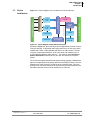
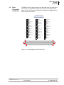
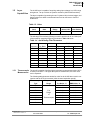
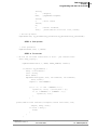
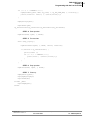
PowerDNA DNA-AI-225
—
User Manual
Simultaneous Sampling, 24-bit, 25-channel
Analog Input layer for the PowerDNA Cube
June 2006 Edition
Version 3.2
PN Man-DNA-AI-225-0606
© Copyright 1998-2007 United Electronic Industries, Inc. All rights reserved.
i
No part of this publication may be reproduced, stored in a retrieval system, or transmitted, in any form
by any means, electronic, mechanical, by photocopying, recording, or otherwise without prior written
permission.
Information furnished in this manual is believed to be accurate and reliable. However, no responsibility
is assumed for its use, or for any infringements of patents or other rights of third parties that may result
from its use.
All product names listed are trademarks or trade names of their respective companies.
See UEI’s website for complete terms and conditions of sale:
http://www.ueidaq.com/company/terms.aspx
Contacting United Electronic Industries
Mailing Address:
611 Neponset Street
Canton, MA 02021
U.S.A.
For a list of our distributors and partners in the US and around the world, please see
http://www.ueidaq.com/partners/
Support:
Telephone:
Fax:
(781) 821-2890
(781) 821-2891
Also see the FAQs and online “Live Help” feature on our web site.
Internet Support:
Support
Web-Site
FTP Site
[email protected]
www.ueidaq.com
ftp://ftp.ueidaq.com
Product Disclaimer:
WARNING!
DO NOT USE PRODUCTS SOLD BY UNITED ELECTRONIC INDUSTRIES, INC. AS CRITICAL
COMPONENTS IN LIFE SUPPORT DEVICES OR SYSTEMS.
Products sold by United Electronic Industries, Inc. are not authorized for use as critical components in
life support devices or systems. A critical component is any component of a life support device or
system whose failure to perform can be reasonably expected to cause the failure of the life support
device or system, or to affect its safety or effectiveness. Any attempt to purchase any United Electronic
Industries, Inc. product for that purpose is null and void and United Electronic Industries Inc. accepts
no liability whatsoever in contract, tort, or otherwise whether or not resulting from our or our
employees' negligence or failure to detect an improper purchase.
ii
1
Table of Contents
Chapter 1 Introduction
.................................................... 1
1.1
Organization of this manual . . . . . . . . . . . . . . . . . . . . . . . . . . . . . . . . . . . . . . . . . . . . 1
1.2
The AI-225 Layer . . . . . . . . . . . . . . . . . . . . . . . . . . . . . . . . . . . . . . . . . . . . . . . . . . . . 3
1.3
Device architecture . . . . . . . . . . . . . . . . . . . . . . . . . . . . . . . . . . . . . . . . . . . . . . . . . . . 4
1.4
1.4.1
Layer Connectors and Wiring . . . . . . . . . . . . . . . . . . . . . . . . . . . . . . . . . . . . . . . . . . . 5
Wiring Diagrams for the AI-225 . . . . . . . . . . . . . . . . . . . . . . . . . . . . . . . . . . . . 6
1.5
1.5.1
Layer capabilities . . . . . . . . . . . . . . . . . . . . . . . . . . . . . . . . . . . . . . . . . . . . . . . . . . . . 7
Thermocouple Measurement . . . . . . . . . . . . . . . . . . . . . . . . . . . . . . . . . . . . . . 7
1.6
1.6.1
Data Representation . . . . . . . . . . . . . . . . . . . . . . . . . . . . . . . . . . . . . . . . . . . . . . . . . . 8
Software Calibration of this Layer . . . . . . . . . . . . . . . . . . . . . . . . . . . . . . . . . . 9
Chapter 2 Programming the High-Level API . . . . . . . . . . . . . . . . . . . . . . . . . . . . . . . . . . 11
2.1
Creating a session . . . . . . . . . . . . . . . . . . . . . . . . . . . . . . . . . . . . . . . . . . . . . . . . . . 11
2.2
Configuring the channels . . . . . . . . . . . . . . . . . . . . . . . . . . . . . . . . . . . . . . . . . . . . . 11
2.3
Configuring the Timing . . . . . . . . . . . . . . . . . . . . . . . . . . . . . . . . . . . . . . . . . . . . . . . 12
2.4
Reading Data . . . . . . . . . . . . . . . . . . . . . . . . . . . . . . . . . . . . . . . . . . . . . . . . . . . . . . 12
2.5
Cleaning-up the Session. . . . . . . . . . . . . . . . . . . . . . . . . . . . . . . . . . . . . . . . . . . . . . 12
Chapter 3 Programming with the Low-Level API . . . . . . . . . . . . . . . . . . . . . . . . . . . . . . 13
3.1
Configuration settings . . . . . . . . . . . . . . . . . . . . . . . . . . . . . . . . . . . . . . . . . . . . . . . . 13
3.2
Channel List Settings . . . . . . . . . . . . . . . . . . . . . . . . . . . . . . . . . . . . . . . . . . . . . . . . 14
3.3
Layer-specific Commands and Parameters . . . . . . . . . . . . . . . . . . . . . . . . . . . . . . . 14
3.4
Using the Layer in ACB Mode. . . . . . . . . . . . . . . . . . . . . . . . . . . . . . . . . . . . . . . . . . 15
3.5
Using Layer in DMap Mode . . . . . . . . . . . . . . . . . . . . . . . . . . . . . . . . . . . . . . . . . . . 17
Appendices
A - Accessories . . . . . . . . . . . . . . . . . . . . . . . . . . . . . . . . . . . . . . . . . . . . . . . . . . . . . . . . . . . 19
DNA-CBL-62 . . . . . . . . . . . . . . . . . . . . . . . . . . . . . . . . . . . . . . . . . . . . . . . . . . . . . . . 19
DNA-STP-AI-U . . . . . . . . . . . . . . . . . . . . . . . . . . . . . . . . . . . . . . . . . . . . . . . . . . . . . 19
DNA-STP-62 . . . . . . . . . . . . . . . . . . . . . . . . . . . . . . . . . . . . . . . . . . . . . . . . . . . . . . . 19
DNA-5B-CONN . . . . . . . . . . . . . . . . . . . . . . . . . . . . . . . . . . . . . . . . . . . . . . . . . . . . . 19
B – Layer Calibration . . . . . . . . . . . . . . . . . . . . . . . . . . . . . . . . . . . . . . . . . . . . . . . . . . . . . . 19
Calibration Procedure . . . . . . . . . . . . . . . . . . . . . . . . . . . . . . . . . . . . . . . . . . . . . . . . . 19
C – Protection Circuits . . . . . . . . . . . . . . . . . . . . . . . . . . . . . . . . . . . . . . . . . . . . . . . . . . . . . 20
© Copyright 2007
United Electronic Industries, Inc.
Date:04. 05. 2007
Vers: 3.2
File: AI 225 User ManualTOC.fm
iv
Table of Figures
Chapter 1 Introduction . . . . . . . . . . . . . . . . . . . . . . . . . . . . . . . . . . . . . . . . . . . . . . . . . . . . 1
1-1
Block Diagram of the DNA-AI-225 Layer ....................................................................... 4
1-2
Pinout Diagram of the AI-225 Layer............................................................................... 5
© Copyright 2007
United Electronic Industries, Inc.
Date:04. 05. 2007
Vers: Draft
File: AI 225 User ManualLOF.fm
DNA-AI-225 Layer
Chapter 1
Introduction
Chapter 1
Introduction
This document outlines the feature-set and use of the AI-225 layer. This layer is
an analog input module for the PowerDNA I/O Cube.
1.1
Organization This PowerDNA AI-225 User Manual is organized as follows:
of this
• Introduction
Manual
This chapter provides an overview of PowerDNA Analog Input
Series board features, the various models available and what
you need to get started.
• The AI-225 layer
This chapter provides an overview of the device architecture,
connectivity, and logic of the AI-225 layer.
• Programming with the High-Level API
This chapter provides an overview of the how to create a session, configure the session for analog input, and interpret results
on the AI-225 series layer.
• Programming with the Low-Level API
This chapter describes low-level API commands for configuring
and using the AI-225 series layer.
• Appendix A: Accessories
This appendix provides a list of accessories available for AI-225
layer(s).
• Appendix B: Calibration
This appendix outlines layer calibration for the AI-225 series
layer.
• Index
This is an alphabetical listing of the topics covered in this manual.
Conventions
To help you get the most out of this manual and our products, we use the following conventions:
Tips are designed to highlight quick ways to get the job done, or to
reveal good ideas you might not discover on your own.
NOTE: Notes alert you to important information.
© Copyright 2006
United Electronic Industries, Inc.
Tel: 781-821-2890
Date: 04. 05. 2007
www.ueidaq.com
Vers: 3.2
File: AI225Chapter1.fm
1
DNA-AI-225 Layer
Chapter 1
Introduction
CAUTION! Caution advises you of precautions to take to avoid injury,
data loss, and damage to your boards or a system crash.
Text formatted in bold typeface generally represents text that should be entered
verbatim. For instance, it can represent a command, as in the following example: “You can instruct users how to run setup using a command such as
setup.exe.”
© Copyright 2006
United Electronic Industries, Inc.
Tel: 781-821-2890
Date: 04. 05. 2007
www.ueidaq.com
Vers: 3.2
File: AI225Chapter1.fm
2
DNA-AI-225 Layer
Chapter 1
Introduction
1.2
AI-225 Layer
Features
The AI-225 layer has the following features:
•
25 A/D simultaneously sampling converters with differential inputs
•
24-bit resolution, ±1.25V input range
• Bipolar range ±1.25V, AIn– and AIn+ within –0.25V–5.0V
• Unipolar range –0.25V..1.25V, AIn– connected to AGND directly
or via up to 10KOhm resistor
• Input underrange/overrange over the ±1.25V range is detected
by the software and reported
© Copyright 2006
United Electronic Industries, Inc.
•
5 S/s to 1000 S/s per channel sampling rates
•
>120dB rejection of AC component of 50/60Hz for sampling rates below
10Hz
•
>120dB Power Supply rejection ratio
•
Typical 120dB of common mode rejection
•
120Hz –3dB analog front-end bandwidth
•
±15V overvoltage and 2kV ESD protection at every input
•
One channel may be used for Cold Junction Compensation (CJC)
•
Entire analog front end isolated from digital circuitry
•
Direct Inputs for thermocouples
•
May be used with RTDs, may be used with external excitation source
(voltage excitation is available on the STP-AI-U)
•
Strain gauge (bridge completion resistors required)
•
Input Impedance 100 Mohm
•
Input bias current ±15nA
•
Non-linearity 3ppm (0.0003%)
•
System noise 0.5μV RMS at 5Hz acquisition rate
•
Effective number of bits: 23.5 @ 5Hz down to 19 @ 1kHz
•
Input ground to system ground isolation: 350Vrms
•
Power consumption 3.9W max
•
SYNC interface option (allows external triggering)
Tel: 781-821-2890
Date: 04. 05. 2007
www.ueidaq.com
Vers: 3.2
File: AI225Chapter1.fm
3
DNA-AI-225 Layer
Chapter 1
Introduction
Figure 1-1 is a block diagram of the architecture of the AI-225 layer.
...
AIn0AIn0+
DC/DC
24-bit
A/D
...
24-bit
A/D
Calibration
Reference
Control
Logic
External Clocks
and Triggers
SRAM
32-bit 66-MHz bus
Analog Input Connector
AIn24+
Optical Isolation
AIn24-
Control Logic
Device
Architecture
Protection/Buffers
1.3
Calibration
EEPROM
Figure 1-1 Block Diagram of the DNA-AI-225 Layer
As shown in Figure 1-1, the AI-225 layer has an independent converter for each
of the 25 channels. A differential input signal goes first to an auto-zero buffer/
amplifier with 125Hz –3dB bandwidth and then to an A/D converter. The A/D
converter accepts signals within a –0.25 to 5V range and measures up to a
±1.25V difference between AIN+ and AIn–. This mode is called referenced
bipolar differential because both AIn+ and AIn- are referenced to system
ground.
The AI-225 uses sigma-delta A/Ds that sample analog signals at 1.8MHz with a
high over-sampling ratio and pass this data into decimating FIR filters. The oversampling ratio varies from 64 to 32768 for various sampling rates. This interworking of A/D converters allows the AI-225 to deliver true 24-bit resolution at a
5Hz data output rate down to 19-bit resolution at a 1 kHz rate.
© Copyright 2006
United Electronic Industries, Inc.
Tel: 781-821-2890
Date: 04. 05. 2007
www.ueidaq.com
Vers: 3.2
File: AI225Chapter1.fm
4
DNA-AI-225 Layer
Chapter 1
Introduction
1.4
Layer
Connectors
and Wiring
The DNA-AI-225 layer supports referenced differential inputs only. Both signal
and return line of the differential signal pair must have a potential within the
range –0.25V to 5V, relative to isolated ground (AGND) level. Figure 1-2 illustrates the pinout of the AI-225.
DB-62 (female)
62-pin connector:
62
61
60
59
58
57
56
55
54
53
52
51
50
49
48
47
46
45
44
43
DIO0
AIN1
AIN2 Return
AIN4
AIN5 Return
AIN7
AIN8 Return
AIN10
AIN11 Return
AIN13
AIN14 Return
AIN16
AIN17 Return
AIN19
AIN20 Return
AIN22
AIN23 Return
AGND
DIO2
RESERVED
42
41
40
39
38
37
36
35
34
33
32
31
30
29
28
27
26
25
24
23
22
AGND
AIN0 Return
AIN2
AIN3 Return
AIN5
AIN6 Return
AIN8
AIN9 Return
AIN11
AIN12 Return
AIN14
AIN15 Return
AIN17
AIN18 Return
AIN20
AIN21 Return
AIN23
AIN24 Return
AGND
RESERVED
RESERVED
21
20
19
18
17
16
15
14
13
12
11
10
9
8
7
6
5
4
3
2
1
9V@20mA
AIN0
AIN1 Return
AIN3
AIN4 Return
AIN6
AIN7 Return
AIN9
AIN10 Return
AIN12
AIN13 Return
AIN15
AIN16 Return
AIN18
AIN19 Return
AIN21
AIN22 Return
AIN24
9V@20mA
DIO1
RESERVED
Figure 1-2. Pinout Diagram of the AI-225 Layer
© Copyright 2006
United Electronic Industries, Inc.
Tel: 781-821-2890
Date: 04. 05. 2007
www.ueidaq.com
Vers: 3.2
File: AI225Chapter1.fm
5
DNA-AI-225 Layer
Chapter 1
Introduction
1.4.1
Wiring
Diagrams for
the AI-225
Table 1-1 shows examples of typical connection diagrams used with various
types of input signals.
Table 1-1. Analog Input Configurations — Differential Inputs (DI) Only
Signal SourceType
Floating Signal Source
Input
Configuration
Grounded Signal Source
Examples:
Examples:
•
•
•
•
Thermocouples
Signal Conditioning with isolated
outputs
Battery devices
Plug-in instruments with non-isolated
inputs
DNA-STP-96 or DNA-STP-AI-U
Sig
+
- Vin
RETx
Ret
AGND
Differential
AINx
AINx
+
- Vin
DNA-STP-96 or DNA-STP-AI-U
AGND
Two resistors (10kohm<R<100 kohm)
provide return paths to ground for bias
currents. See DNA-STP-AI-U jumpers
(JDx/JGx/Nx).
Sig
+
- Vin
Ret
AINx
Single-ended
Ground
Referenced
(not valid for
standard AI-225)
Not Used
AGND
Table 1-2. Analog Input Configurations — RTD, Bridge Wiring
DNA-STP-96 or DNA-STP-AI-U
+5V 20k
1K
AInX+
RTD
AInX–
AGND
© Copyright 2006
United Electronic Industries, Inc.
Tel: 781-821-2890
Date: 04. 05. 2007
www.ueidaq.com
Vers: 3.2
File: AI225Chapter1.fm
6
DNA-AI-225 Layer
Chapter 1
Introduction
1.5
Layer
Capabilities
The AI-225 layer is capable of acquiring analog input voltages in ±1.25V range
with gains of 1 at up to 24 bits of dynamic resolution (222nV RMS resolution).
The layer is capable of generating its own CL (channel list) clock and trigger, and
deriving them from either local external lines from its connector or from the
SYNCx bus.
Table 1-3. Gains
Card
Gain
Range
Noise, LSB
Resolution.
noise limited
AI-225
1
±V1.25
1.5‘
222nV
The aAnalog RC anti-aliasing filtering is tuned to provide roll-off at 1.5kHz (half
of the maximum sampling frequency) as shown in Table 1-4 below.
Table 1-4. Anti-Aliasing Filter Parameters
Oversampl
Frequency ing Ratio
1.5.1
Noise
ENOBs
ADC
System
ADC
System
1000
128
3.5µV
5µV
20
18
800
256
2µV
3µV
21.3
21
400
512
1.4µV
2µV
21.8
21
200
1024
1µV
1.5µV
22.4
22
100
2048
750nV
1µV
22.9
22
50
4096
510nV
900nV
23.4
23
25
8192
375nV
700nV
24
24
10
16384
250nV
600nV
24.4
24
Thermocouple The AI-225 is capable of performing thermocouple measurements within 0.02°C
Measurement at 10Hz per channel. The higher the speed of measurement, the more noise
can be expected.
The following table shows test results for noise for the AI-225 when used in conjunction with the STP-AI-U terminal (10Hz/ channel acquisition speed):
Thermocouple
Type
P-p Noise, °C
100 Points
RMS Noise, °C
B
0.50
0.16
C
0.24
0.07
0.06
0.02
0.07
0.02
0.10
0.03
0.12
0.03
R
0.32
0.1
S
0.37
0.1
E
J
K
N
© Copyright 2006
United Electronic Industries, Inc.
Tel: 781-821-2890
Date: 04. 05. 2007
Temperature
Range
Full
Range
of
Thermocouples
www.ueidaq.com
Vers: 3.2
File: AI225Chapter1.fm
7
DNA-AI-225 Layer
Chapter 1
Introduction
Additional factors:
1.6
Data
Representation
•
Open TC detection circuitry on the DNA-STP-AI-U adds ~15μV (±2μV)
constant offset on all channels. (May be compensated using the CJC
temperature sensor calibration. Channel-channel difference may be
adjusted using the offset calibration simod 3 command.)
•
CJC sensor is calibrated to better than 0.2°C accuracy at room temperature
•
Stays within 0.4°C accuracy from –20 to +75°C temperature
The AI-225 layer is equipped with 25 24-bit A/D converters. The layer can return
24-bit two’s complement data in 32-bit words, combined with levels on generalpurpose digital I/O lines.
By default, if acquisition is not running, the output buffer is filled with relative
addresses. On reset, every entry in the output buffer is filled with its relative position number. If you start receiving consecutive data from the layer (such as
0,1,2,..) it means that either the layer is not initialized properly or it is damaged.
The following definition converts raw data from the converter into a 24-bit
straight binary value:
#define LT2440_GETVAL(V) (((V>>5)&0xffffff)^0x800000)
To convert data into floating point, use the following formula (V is a result from
the DQ_LT2440_GETVAL() macro):
Volts = (V) * (2.5V/2^24) – 1.25V
Raw 32-bit data received from converter is represented as:
Reset
State
Bit
Name
Description
31
EOC
Zero, if conversion is completed.
0
30
DMY
Always low.
0
29
SIG
Sign bit of the conversion. If VIN is > 0, this bit is
NA
HIGH. If VIN is < 0, this bit is LOW.
28
MSB
Most significant bit of the result. If both Bit 29
and Bit 28 are HIGH, the differential input
voltage is above +FS. If both Bit 29 and Bit 28
are LOW, the differential input voltage is below
–FS.
NA
27-5
LSB
Less significant bits of the result.
NA
5-3
© Copyright 2006
United Electronic Industries, Inc.
SubLSB Sub LSB of the result beyond 24-bit level. Can
be used in averaging.
NA
1
DIO2
Level of DIO1 line (output).
0
1
DIO1
Level of DIO1 line (input).
0
0
DIO0
Level of DIO0 line (input).
0
Tel: 781-821-2890
Date: 04. 05. 2007
www.ueidaq.com
Vers: 3.2
File: AI225Chapter1.fm
8
DNA-AI-225 Layer
Chapter 1
Introduction
1.6.1
Software
Calibration of
this Layer
Unlike most PowerDNA layers, the AI-225 relies on software calibration on the
host side.
The idea of layer calibration is to read, average, and store readings from all
channels at zero volts and then at the fixed level (1V is the default level).
By subtracting actual readings at zero volts from the ideal value (0x800000,
straight binary) the software calculates calibration offsets.
The firmware then subtracts the offset-adjusting value from the average value
read at 1V. The result represents an offset-compensated reading at 1V. By dividing actual calibration voltage by offset-compensated reading, the software calculates the actual channel gain.
When DQE opens the IOM, it automatically downloads calibration coefficients
from each AI-225 in the PowerDNA cube by issuing DQCMD_RDFIFO commands
with FIFO_GET_CAL FIFO channel.
In return, the firmware sends a CALSET_225_ structure, which contains the
gain calibration level and the averaged readings at zero volts and that level.
Then, the software stores offset-adjusting values directly and calculates actual
gain for every channel, as follows:
cfvolt = (cvolt/ONEVOLTINNV);
for (all channels) gain[i] = cfvolt/pcval[i];
You need to perform data calibration only when you configure and use the
AI-225 layer directly, without DQE running.
© Copyright 2006
United Electronic Industries, Inc.
Tel: 781-821-2890
Date: 04. 05. 2007
www.ueidaq.com
Vers: 3.2
File: AI225Chapter1.fm
9
DNA-AI-225 Layer
Chapter 2
Programming the High-Level API
Chapter 2
Programming the High-Level API
This section describes how to program the PowerDNA AI-225 using the
UeiDaq’s framework API.
Since the UeiDaq Framework is object oriented, its objects can be manipulated
in the same manner from different development environments such as Visual
C++, Visual Basic, or LabVIEW.
Although the following section focuses on the C++ API, the concept is the same
no matter what programming language you use.
Please refer to the “UeiDaq Framework User Manual” for more information on
using other programming languages.
2.1
Creating a
Session
The Session object controls all operations on your PowerDNA device. The first
task, therefore, is to create a session object, as follows:
CUeiSession session;
2.2
Configuring
the
Channels
Framework uses resource strings to select which device, subsystem, and channels to use within a session. The resource string syntax is similar to a web URL:
<device class>://<IP address>/<Device Id>/<Subsystem><Channel list>
For PowerDNA the device class is pdna.
For example, the following resource string selects analog input channels 0,2,3,4
on device 1 at IP address 192.168.100.2:
“pdna://192.168.100.2/Dev1/Ai0,2,3,4”
The session object’s method “CreateAIChannel” is used to configure the channel list, gain, and signal referencing mode. The gain and input mode parameters
are ignored when using an AI-225 because it doesn’t have programmable gain
and is differential only).
// Configure session to acquire from channels 0 and 1
session.CreateAIChannel(“pdna://192.168.100.2/Dev0/Ai0,1”, -0.15,
0.15, UeiAIChannelInputModeDifferential);
The AI-225 offers very good accuracy, thanks to its 24-bit A/D converters and its
dedicated channel for measuring the Cold Junction Compensation temperature
sensor. Therefore, it is well suited for measuring temperature with thermocouples.
The session object’s method “CreateTCChannel” is used to configure the channels, thermocouple type, CJC sensor, and temperature scale.
You can use thermocouples of type E, J, K, R, S, T, B or N.
You can measure the CJC temperature either by using a sensor integrated in the
terminal block or by specifying a constant.
You can measure temperature in degrees Celsius, Fahrenheit, Kelvin, or Rankine.
// Configure the session to acquire temperatures in degrees
© Copyright 2007
United Electronic Industries, Inc.
Tel: 781-821-2890
Date: 04. 05. 2007
www.ueidaq.com
Vers: 3.2
File: AI225Chapter2.fm
10
DNA-AI-225 Layer
Chapter 2
Programming the High-Level API
// Celsius from channels 0 and 1 using K thermocouples.
// Use the built-in CJC sensor
session.CreateTCChannel(“pdna://192.168.100.2/Dev0/Ai0,1”, -100.0,
100.0, UeiThermocoupleTypeK, UeiTemperatureScaleCelsius,
UeiCJCTypeBuiltIn, 0.0, “”, UeiAIChannelInputModeDifferential);
2.3
Configuring
the Timing
You can configure the AI-225 to run in simple mode (point by point) or buffered
mode (ACB mode).
In simple mode, the delay between samples is determined by software on the
host computer.
In buffered mode, the delay between samples is determined by the AI-225 onboard clock.
The following sample shows how to configure the simple mode. Please refer to
the “UeiDaq Framework User Manual” to learn how to use the other timing
modes.
session.ConfigureTimingForSimpleIO();
2.4
Reading
Data
Reading data from the AI-225 is done using a reader object. There is a reader
object to read raw data coming straight from the A/D converter. There is also a
reader object to read data already scaled to volts or temperatures.
The following sample code shows how to create a scaled reader object and read
samples.
// Create a reader and link it to the session’s stream
CueiAnalogScaledReader reader(session.GetDataStream());
// read one scan, the buffer must be big enough to contain
// one value per channel
double data[2];
reader.ReadSingleScan(data);
2.5
Cleaning-up
the Session
The session object cleans itself up when it goes out of scope or when it is
destroyed. However, to reuse the object with a different set of channels or
parameters, you can also clean up the session manually.
session.CleanUp();
© Copyright 2007
United Electronic Industries, Inc.
Tel: 781-821-2890
Date: 04. 05. 2007
www.ueidaq.com
Vers: 3.2
File: AI225Chapter2.fm
11
DNA-AI-225 Layer
Chapter 3
Programming with the Low-Level API
Chapter 3
Programming with the Low-Level API
This section describes how to program the PowerDNA cube using the low-level
API. The low-level API offers direct access to PowerDNA DAQBios protocol and
also allows you to directly access device registers.
We recommend that you use the UeiDaq Framework (see Chapter 2), because
it is easier to use.
You should only need to use the low-level API if you are using an operating system other than Windows.
3.1
Configuration Configuration setting are passed in DqCmdSetCfg() and
DqAcbInitOps() functions.
Settings
Note that not all configuration bits apply to AI-225 layer.
The following bits make sense:
#define DQ_FIFO_MODEFIFO (2L << 16) // continuous acquisition with FIFO
#define DQ_LN_MAPPED
(1L<<15)
#define DQ_LN_STREAMING
(1L<<14)
// For WRRD (DMAP) devices
// For RDFIFO devices - stream the
// FIFO data automatically
// For WRFIFO - do NOT send reply
// to WRFIFO unless needed
#define DQ_LN_IRQEN
(1L<<10)
// enable layer irqs
#define DQ_LN_PTRIGEDGE1 (1L<<9)
#define DQ_LN_PTRIGEDGE0 (1L<<8)
// stop trigger edge MSB
// stop trigger edge:
// 00 - software,
// 01 - rising, 02 - falling
#define DQ_LN_STRIGEDGE1 (1L<<7)
#define DQ_LN_STRIGEDGE0 (1L<<6)
// start trigger edge MSB
// start trigger edge:
// 00 -software, 01 - rising,
// 02 - falling
#define DQ_LN_CVCKSRC1
(1L<<5)
// CV clock source MSB
#define DQ_LN_CVCKSRC0
(1L<<4)
// CV clock source 01 - SW, 10 - HW, 11 -EXT
#define DQ_LN_CLCKSRC1
(1L<<3)
// CL clock source MSB
#define DQ_LN_CLCKSRC0
(1L<<2)
// CL clock source 01 - SW, 10 - HW, 11 -EXT
#define DQ_LN_ACTIVE
(1L<<1)
// "STS" LED status
#define DQ_LN_ENABLED
(1L<<0)
// enable operations
For streaming operations with hardware clocking, select the following flags:
DQ_LN_ENABLE | DQ_LN_CVCKSRC0 | DQ_LN_STREAMING | DQ_LN_IRQEN | DQ_LN_ACTIVE
DQ_LN_ENABLE enables all operations with the layer.
DQ_LN_CVCKSRC0 selects the internal channel list clock (CL) source as a timebase. The AI-225 supports CV clock.
DQ_LN_ACTIVE is needed to switch on the “STS” LED on the CPU layer.
You can select either the CL or CV clock as a timebase. Because of the parallel
architecture of AI-225 layer, either clock triggers all converters.
Aggregate rate = Per-channel rate * Number of channels
© Copyright 2007
United Electronic Industries, Inc.
Tel: 781-821-2890
Date: 04. 05. 2007
www.ueidaq.com
Vers: 3.2
File: AI225Chapter3.fm
12
DNA-AI-225 Layer
Chapter 3
Programming with the Low-Level API
Acquisition rate cannot be selected on per-channel basis. To select a different
resulting rate for a different channel, program the proper decimators in the FIR
unit.
3.2
Channel List The AI-225 layer has a very simple channel list structure, as shown in the table
below.:
Settings
Bit
Name
31
DQ_LNCL_NEXT
Tells firmware there is a “next” entry in the
channel list.
20
DQ_LNCL_TSRQ
Request timestamp as a next data point
7..0
3.3
Layerspecific
Commands
and
Parameters
Purpose
Channel number
Layer-specific functions are described in the DaqLibHL.h file.
DqAdv225Read()
This function works using underlying DqReadAIChannel(), but converts the
data using internal knowledge of the input range and calibrates every channel. It
uses DQCMD_IOCTL with DQIOCTL_CVTCHNL under the hood.
When this function is called for the first time, the firmware stops any ongoing
operation on the device specified and reprograms it according to the channel list
supplied. This function uses the preprogrammed CL update frequency —
13.75Hz. You can reprogram the update frequency by calling
DqCmdSetClk()after the first call to DqAdv225Read().
Therefore, you cannot perform this function call when the layer is involved in any
streaming or data mapping operations.
If you specify a short timeout delay, this function can time out when called for the
first time because it is executed as a pending command and layer programming
takes up to 10ms.
Once this function is called, the layer continuously acquires data and every call
to the function returns the latest acquired data.
If you want to cancel ongoing sampling, call the same function with
0xFFFFFFFF as a channel number.
© Copyright 2007
United Electronic Industries, Inc.
Tel: 781-821-2890
Date: 04. 05. 2007
www.ueidaq.com
Vers: 3.2
File: AI225Chapter3.fm
13
DNA-AI-225 Layer
Chapter 3
Programming with the Low-Level API
3.4
Using the
Layer in ACB
Mode
The following is a pseudo-code example that highlights the functions needed in
sequence to use ACB on the 225 layer. A complete example with error checking
can be found in the directory SampleACB205.
#include "PDNA.h"
// unit configuration word
#define CFG225
(DQ_LN_ENABLED \
|DQ_LN_ACTIVE \
|DQ_LN_GETRAW \
|DQ_LN_IRQEN \
|DQ_LN_CLCKSRC0 \
|DQ_LN_STREAMING \
|DQ_AI225_MODEFIFO)
uint32 Config = CFG225;
STEP 1: Start DQE engine.
#ifndef _WIN32
DqInitDAQLib();
#endif
// Start engine
DqStartDQEngine(1000*1, &pDqe, NULL);
// Open communication with IOM
hd0 = DqOpenIOM(IOM_IPADDR0, DQ_UDP_DAQ_PORT, TIMEOUT_DELAY, &RdCfg);
// Receive IOM crucial identification data
DqCmdEcho(hd0, DQRdCfg);
// Set up channel list
for (n = 0; n < CHANNELS; n++) {
CL[n] = n;
}
STEP 2: Create and initialize host and IOM sides.
// Now we are going to test device
DqAcbCreate(pDqe, hd0, DEVN, DQ_SS0IN, &bcb);
// Let’s assume that we are dealing with AI-201 device
dquser_initialize_acb_structure();
// Now call the function
ret = DqAcbInitOps(bcb,
© Copyright 2007
United Electronic Industries, Inc.
Tel: 781-821-2890
Date: 04. 05. 2007
www.ueidaq.com
Vers: 3.2
File: AI225Chapter3.fm
14
DNA-AI-225 Layer
Chapter 3
Programming with the Low-Level API
&Config,
0,
//TrigSize,
NULL,
//pDQSETTRIG TrigMode,
&fCLClk,
0,
//float* fCVClk
&CLSize,
CL,
0,
//uint32* ScanBlock,
&acb);
printf("Actual clock rate: %f\n", fCVClk);
// Now set up events
DqeSetEvent(bcb, DQ_eFrameDone|DQ_ePacketLost|DQ_eBufferError|DQ_ePacketOOB);
STEP 3: Start operation.
// Start operations
DqeEnable(TRUE, &bcb, 1, FALSE);
STEP 4: Process data.
// We will not use event notification at first - just retrieve scans
while (keep_looping) {
DqeWaitForEvent(&bcb, 1, FALSE, EVENT_TIMEOUT, &events);
if (events & DQ_eFrameDone) {
minrq = acb.framesize;
avail = minrq;
while (TRUE) {
DqAcbGetScansCopy(bcb, data, acb.framesize, acb.framesize,
&size, &avail);
samples += size*CHANNELS;
for (i = 0; i < size * CHANNELS; i++) {
fprintf(fo, "%f\t", *((float*)data + i));
if ((i % CHANNELS) == (CHANNELS - 1)) {
fprintf(fo, "\n");
}
}
printf("eFD:%d scans received (%d samples) min=%d avail=%d\n", size,
samples, minrq, avail);
if (avail < minrq) {
break;
}
}
}
© Copyright 2007
United Electronic Industries, Inc.
Tel: 781-821-2890
Date: 04. 05. 2007
www.ueidaq.com
Vers: 3.2
File: AI225Chapter3.fm
15
DNA-AI-225 Layer
Chapter 3
Programming with the Low-Level API
}
STEP 5: Stop operation.
DqeEnable(FALSE, &bcb, 1, FALSE);
STEP 6: Clean up.
DqAcbDestroy(bcb);
DqStopDQEngine(pDqe);
DqCloseIOM(hd0);
#ifndef _WIN32
DqCleanUpDAQLib();
#endif
3.5
Using Layer
in DMap
Mode
#include "PDNA.h"
STEP 1: Start DQE engine
#ifndef _WIN32
DqInitDAQLib();
#endif
// Start engine
DqStartDQEngine(1000*10, &pDqe, NULL);
// open communication with IOM
hd0 = DqOpenIOM(IOM_IPADDR0, DQ_UDP_DAQ_PORT, TIMEOUT_DELAY, &DQRdCfg);
// Receive IOM crucial identification data
DqCmdEcho(hd0, DQRdCfg);
for (i = 0; i < DQ_MAXDEVN; i++) {
if (DQRdCfg->devmod[i]) {
printf("Model: %x Option: %x\n", DQRdCfg->devmod[i], DQRdCfg->option[i]);
} else {
break;
}
}
STEP 2: Create and initialize host and IOM sides.
DqDmapCreate(pDqe, hd0, &pBcb, UPDATE_PERIOD, &dmapin, &dmapout);
STEP 3: Add channels into DMap.
© Copyright 2007
United Electronic Industries, Inc.
Tel: 781-821-2890
Date: 04. 05. 2007
www.ueidaq.com
Vers: 3.2
File: AI225Chapter3.fm
16
DNA-AI-225 Layer
Chapter 3
Programming with the Low-Level API
for (i = 0; i < CHANNELS; i++) {
DqDmapSetEntry(pBcb, DEVN, DQ_SS0IN, i, DQ_ACB_DATA_RAW, 1, &ioffset[i]);
printf("offset%d = 0x%x\n", i, (uint32)ioffset[i]);
}
DqDmapInitOps(pBcb);
DqeSetEvent(pBcb,
DQ_eDataAvailable|DQ_ePacketLost|DQ_eBufferError|DQ_ePacketOOB);
STEP 4: Start operation.
DqeEnable(TRUE, &pBcb, 1, FALSE);
STEP 5: Process data.
while (keep_looping) {
DqeWaitForEvent(&pBcb, 1, FALSE, timeout, &eventsin);
if (eventsin & DQ_eDataAvailable) {
printf("\ndata ");
for (i = 0; i < CHANNELS; i++) {
printf("%08x ", *(uint32*)ioffset[i]);
}
}
}
STEP 6: Stop operation.
DqeEnable(FALSE, &pBcb, 1, FALSE);
STEP 7: Clean up.
DqDmapDestroy(pBcb);
DqStopDQEngine(pDqe);
DqCloseIOM(hd0);
#ifndef _WIN32
DqCleanUpDAQLib();
#endif
© Copyright 2007
United Electronic Industries, Inc.
Tel: 781-821-2890
Date: 04. 05. 2007
www.ueidaq.com
Vers: 3.2
File: AI225Chapter3.fm
17
DNA-AI-225 Layer
Appendices
A - Accessories
The following cables and STP boards are available for the AI-201 layer.
DNA-CBL-62
2.5ft, 62-way round shielded cable
DNA-STP-AI-U
Universal PowerDNA Analog Input Terminal Panel
DNA-STP-62
62-channel screw terminal panel
DNA-5B-CONN
24-channel signal-conditioning mating panel
B – Layer
Calibration
Note that once you perform layer calibration yourself, factory calibration warranty is void.
Calibration should be performed with microvolt-resolution precision voltage
source with low (1 Ohm or less) output impedance. Calibration assumes use of
the single-ended mode, where all channels have the same signal and return levels. Please tie AGND to the common return of all channels with a 10k resistor to
keep it closer to the common mode level.
To perform layer calibration, you should have a precision voltage source
attached to all twenty-five channels and run a serial terminal program attached
to the IOM serial port.
Use the “simod 1” command to calibrate the layer.
Calibration Procedure (using serial port terminal):
STEP 1: Apply 0V on all channels
STEP 2: Type “simod 1”
STEP 3: From the device table, select the proper device to be calibrated .
The firmware will ask you to apply 0V and press Enter when this is done. The
firmware then acquires multiple scans for averaging within ten seconds.
The firmware will ask you to apply 1V and press Enter when this is done.
STEP 4: Apply 1V and press Enter. The firmware then acquires multiple scans for
averaging within ten seconds.
The firmware calculates the offset adjustment and gain and displays them. For
a normally working layer, the gain should be within 151..156 nV/bit. Values outside this range suggest either high noise levels, problems with the voltages
applied, or a hardware problem with the layer.
STEP 5: Press “Esc” and reply “y” if you want to save the calibration values into
E2PROM.
STEP 6: To verify calibration, reset the PowerDNA cube.
NOTE: The AI-225 layer is extremely sensitive (1bit = 152nV) and can react to
your movements near voltage source cabling and input connectors. We
recommend locating the voltage source and PowerDNA cube being
© Copyright 2006
United Electronic Industries, Inc.
Tel: 781-821-2890
Date: 04. 05. 2007
www.ueidaq.com
Vers: 3.2
File: AI225Appx.fm
18
DNA-AI-225 Layer
calibrated as far away from the operator and sources of EM noise as
possible.
We also recommend calibrating the offset by applying 0 volts from the
signal source rather than by shorting inputs
You can verify calibration after resetting the PowerDNA cube by using
the same “simod 1” routine, but do not save the results at the end.
“simod 2” shows raw acquired data without filtering as well as RMS and
delta readings.
For AI-225 layers, we recommend annual factory recalibration at UEI
C – Protection
Circuits
At times, the signal being measured appears to clip when attempting to measure what appear to be normal voltages. Clipping is a sign of tripping the protection circuitry of the layer, which is designed to protect layer components from
damage by high voltage. This can happen under a variety of conditions, such
as a different potential for the AI-225’s ground vs. the chassis of the instrument
(this can be fixed by connecting the chassis to the AGND line on the STP-AI-U).
Given the variables:
Let VEE = 0V (this is AGND)
Let VCC = 5V (or anywhere between 4.75V to 5.25V, depending on the P.S.U.)
Breaking the following rules activates the protection circuitry:
1. VCC + 0.25V > VIN(-) > VEE – 0.25V
VCC + 0.25V > VIN(+) > VEE – 0.25V
2. | VIN(-) – VIN(+) | < 1.25V
© Copyright 2006
United Electronic Industries, Inc.
Tel: 781-821-2890
Date: 04. 05. 2007
www.ueidaq.com
Vers: 3.2
File: AI225Appx.fm
19
20
Index
A
A/D Converters 3
A/D Resolution 3
Accessories 18
Anti-Alias Filtering
Architecture 4
B
Block Diagram
C
G
Gains
H
High-Level API
7
I
L
Layer Commands and Parameters
Low-Level API 12
Calibration 9
How-to 18
calibration
How-to 19
Calibration Procedure 18
Capabilities 7
Channel List Settings 13
Channel List Structure 13
Cleaning-up the Session 11
Configuration Bits 12
Configuration Settings 12
Configuring Channels 10
Configuring Timing 11
Connectors and Wiring 5
Conventions 1
Creating a Session 10
Data Representation
E
ESD Protection
F
Features
M
Mailing Address
Mode
ACB 14
DMap 16
13
ii
O
Organization 1
Overvoltage Protection 3
P
Pinout 5
Product Disclaimer
R
Reading Data
S
ii
11
Sampling Rate 3
Software Calibration
Support ii
8
9
T
3
Thermocouple Measurement
W
3
© Copyright 2007
United Electronic Industries, Inc.
10
Input Configurations 6
Internet Support ii
4
D
7
Wiring Diagrams
Tel: 781-821-2890
Date: 04. 05. 2007
7
6
www.ueidaq.com
File:
Vers: 1.0
AI 225 User ManualIX.fm