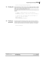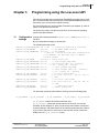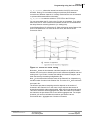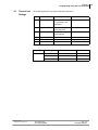
1
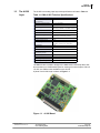
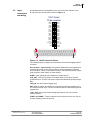
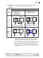
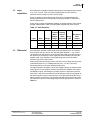
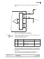
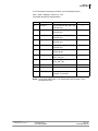
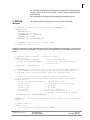
DNA-AI-202 Analog Current Input Layer User Manual Sequential Sampling 16-bit 12-channel Analog Current Input layer for the PowerDNA Cube February 2009 Edition PN Man-DNA-AI-202-0209 Version 1.4 © Copyright 1998-2009 United Electronic Industries, Inc. All rights reserved. i No part of this publication may be reproduced, stored in a retrieval system, or transmitted, in any form by any means, electronic, mechanical, by photocopying, recording, or otherwise without prior written permission. Information furnished in this manual is believed to be accurate and reliable. However, no responsibility is assumed for its use, or for any infringements of patents or other rights of third parties that may result from its use. All product names listed are trademarks or trade names of their respective companies. See UEI’s website for complete terms and conditions of sale: http://www.ueidaq.com/company/terms.aspx Contacting United Electronic Industries Mailing Address: 27 Renmar Ave. Walpole, MA 02081 U.S.A. For a list of our distributors and partners in the US and around the world, please see http://www.ueidaq.com/partners/ Support: Telephone: Fax: (508) 921-4600 (508) 668-2350 Also see the FAQs and online “Live Help” feature on our web site. Internet Support: Support [email protected] Web-Site www.ueidaq.com FTP Site ftp://ftp.ueidaq.com Product Disclaimer: WARNING! DO NOT USE PRODUCTS SOLD BY UNITED ELECTRONIC INDUSTRIES, INC. AS CRITICAL COMPONENTS IN LIFE SUPPORT DEVICES OR SYSTEMS. Products sold by United Electronic Industries, Inc. are not authorized for use as critical components in life support devices or systems. A critical component is any component of a life support device or system whose failure to perform can be reasonably expected to cause the failure of the life support device or system, or to affect its safety or effectiveness. Any attempt to purchase any United Electronic Industries, Inc. product for that purpose is null and void and United Electronic Industries Inc. accepts no liability whatsoever in contract, tort, or otherwise whether or not resulting from our or our employees' negligence or failure to detect an improper purchase. ii iii Table of Contents Chapter 1 Introduction .................................................... 1 1.1 1.1.1 1.1.2 1.1.3 1.1.4 Organization of this manual . . . . . . . . . . . . . . . . . . . . . . . . . . . . . . . . . . . . . . . . . . . . Introduction . . . . . . . . . . . . . . . . . . . . . . . . . . . . . . . . . . . . . . . . . . . . . . . . . . . The AI-202 layer . . . . . . . . . . . . . . . . . . . . . . . . . . . . . . . . . . . . . . . . . . . . . . . Programming with the High Level API . . . . . . . . . . . . . . . . . . . . . . . . . . . . . . . Programming using the Low Level API . . . . . . . . . . . . . . . . . . . . . . . . . . . . . . 1 1 1 1 1 1.2 The AI-202 Layer . . . . . . . . . . . . . . . . . . . . . . . . . . . . . . . . . . . . . . . . . . . . . . . . . . . . 3 1.3 Device architecture . . . . . . . . . . . . . . . . . . . . . . . . . . . . . . . . . . . . . . . . . . . . . . . . . . . 4 1.4 1.4.1 Layer connectors and wiring . . . . . . . . . . . . . . . . . . . . . . . . . . . . . . . . . . . . . . . . . . . . 5 Analog Input Ground Connections. . . . . . . . . . . . . . . . . . . . . . . . . . . . . . . . . . 6 1.5 Layer capabilities . . . . . . . . . . . . . . . . . . . . . . . . . . . . . . . . . . . . . . . . . . . . . . . . . . . . 7 1.6 Differential. . . . . . . . . . . . . . . . . . . . . . . . . . . . . . . . . . . . . . . . . . . . . . . . . . . . . . . . . . 7 1.7 Data Representa-tion . . . . . . . . . . . . . . . . . . . . . . . . . . . . . . . . . . . . . . . . . . . . . . . . . 8 Chapter 2 Programming with the High Level API . . . . . . . . . . . . . . . . . . . . . . . . . . . . . . 10 2.1 Creating a session . . . . . . . . . . . . . . . . . . . . . . . . . . . . . . . . . . . . . . . . . . . . . . . . . . 10 2.2 Configuring the channels . . . . . . . . . . . . . . . . . . . . . . . . . . . . . . . . . . . . . . . . . . . . . 10 2.3 Configuring the timing . . . . . . . . . . . . . . . . . . . . . . . . . . . . . . . . . . . . . . . . . . . . . . . . 10 2.4 Reading data. . . . . . . . . . . . . . . . . . . . . . . . . . . . . . . . . . . . . . . . . . . . . . . . . . . . . . . 11 2.5 Cleaning-up the session . . . . . . . . . . . . . . . . . . . . . . . . . . . . . . . . . . . . . . . . . . . . . . 11 Chapter 3 Programming using the Low-Level API . . . . . . . . . . . . . . . . . . . . . . . . . . . . . 12 3.1 Configuration settings . . . . . . . . . . . . . . . . . . . . . . . . . . . . . . . . . . . . . . . . . . . . . . . . 12 3.2 Channel List Settings . . . . . . . . . . . . . . . . . . . . . . . . . . . . . . . . . . . . . . . . . . . . . . . . 14 3.3 3.3.1 3.3.2 Layer-specific commands and parameters . . . . . . . . . . . . . . . . . . . . . . . . . . . . . . . . 15 Using layer in ACB mode . . . . . . . . . . . . . . . . . . . . . . . . . . . . . . . . . . . . . . . . 15 Using layer in DMap mode. . . . . . . . . . . . . . . . . . . . . . . . . . . . . . . . . . . . . . . 18 Appendices. . . . . . . . . . . . . . . . . . . . . . . . . . . . . . . . . . . . . . . . . . . . . . . . . . . . . . . . . . . . . . . 19 Index . . . . . . . . . . . . . . . . . . . . . . . . . . . . . . . . . . . . . . . . . . . . . . . . . . . . . . . . . . . . . . . . . . 20 © Copyright 2009 United Electronic Industries, Inc. Tel: 508-921-4600 Date: February 2009 Vers: 1.4 File:AI-202TOC.fm iv List of Figures Chapter 1 Introduction . . . . . . . . . . . . . . . . . . . . . . . . . . . . . . . . . . . . . . . . . . . . . . . . . . . . 1 1-1 AI-202 Board.................................................................................................................. 3 1-2 AI-202 Architecture Block Diagram................................................................................ 4 1-3 AI-202 Connector Pinout................................................................................................ 5 1-4 Recommended Ground Connections for Analog Inputs ................................................ 6 1-5 Typical DNA-AI-202 Input Wiring ................................................................................... 8 Chapter 2 Programming with the High Level API . . . . . . . . . . . . . . . . . . . . . . . . . . . . . . 10 (None) Chapter 3 Programming using the Low-Level API . . . . . . . . . . . . . . . . . . . . . . . . . . . . . 12 3-1 CL and. CV Clock Timing............................................................................................. 13 © Copyright 2009 United Electronic Industries, Inc. Tel: 508-921-4600 Date: February 2009 Vers: 1.4 File:AI-202LOF.fm Chapter 1 Introduction Chapter 1 Introduction This document outlines the feature-set and use of the PowerDNA DNA-AI-202 layer. This layer is an analog input module for the PowerDNA I/O Cube designed for current input signals. 1.1 Organization This DNA-AI-202 User Manual is organized as follows: of this manual 1.1.1 Introduction This section provides an overview of PowerDNA Analog Input Series board features, the various models available, and what you need to get started. 1.1.2 The AI-202 layer This chapter provides an overview of the device architecture, connectivity, and logic of the AI-202 layer. 1.1.3 Programming with the High Level API This chapter provides an overview of the how to create a session, configure the session for digital data acquisition/output, and format relevant output. 1.1.4 Programming This chapter describes the low-level API commands for configuring and using using the Low the AI-202 layer. Level API Appendices A. Accessories This appendix provides a list of accessories available for the AI-202 layer. B. Layer Calibration This appendix outlines calibration procedures for the AI-202 series layer. Index This is an alphabetical listing of the topics covered in this manual. © Copyright 20099 United Electronic Industries, Inc. Tel: 508-921-4600 Date: February 2009 Vers: 1.4 File:AI-202 Chap1.fm 1 Chapter 1 Introduction Manual Conventions To help you get the most out of this manual and our products, please note that we use the following conventions: Tips are designed to highlight quick ways to get the job done, or reveal good ideas you might not discover on your own. NOTE: Notes alert you to important information. Caution advises you of precautions to take to avoid injury, data loss, and damage to your boards or a system crash. Text formatted in bold typeface generally represents text that should be entered verbatim. For instance, it can represent a command, as in the following example: “You can instruct users how to run setup using a command such as setup.exe.” © Copyright 20099 United Electronic Industries, Inc. Tel: 508-921-4600 Date: February 2009 Vers: 1.4 File:AI-202 Chap1.fm 2 Chapter 1 Introduction 1.2 The AI-202 Layer The AI-202 is an analog input layer with specifications as listed in Table 1-1. Table 1-1 DNA-AI-202 Technical Specifications p Resolution Number of Channels: Differential Maximum Sampling Rate Onboard FIFO Size Input Ranges Shunt Resistance Input Bias Current Input Overvoltage Isolation A/D Conversion Time A/D Settling Time Nonlinearity System Noise Effective Number of Bits Total Harmonic Distortion+ Nonlinearity+Noise Channel Crosstalk Power Consumption Operating Temp. (tested) Operating Humidity 16 bits 12 16 kS/s, aggregate 512 samples ±1.5 mA, ±15 mA, ±150 mA (use when measuring 0-20mA or 4-20mA sensors) 10Ý 0.1% ±15 nA ±40V, 2000V ESD, powered or unpowered, 20mA max current 1500Vrms 2 μsec 22 μsec (±150 mA scale), 100 μsec (±15 mA scale), 1 msec (±1.5 mA scale) 1 LSB 1.2 LSB 14.8 91 dB 85 dB @ 1 kS/s 1.8W -40°C to +85°C 90%, non-condensing The DNA-AI-202 is similar in design to the DNA-AI-201-100 except that it has shunt resistors on 12 differential inputs for sensing mA current inputs. Gains of 10, 100, and 1000 are also available on the AI-202. A photo of an AI-202 Layer s shown in Figure 1-1. Figure 1-1. AI-202 Board © Copyright 20099 United Electronic Industries, Inc. Tel: 508-921-4600 Date: February 2009 Vers: 1.4 File:AI-202 Chap1.fm 3 Chapter 1 Introduction 1.3 Device architecture The AI-202 layer is physically divided into isolated (IS) and non-isolated (NIS) parts, as illustrated in the block diagram of Figure 1-2. The non-isolated part is powered from DC/DC converters located on the CPU layer. These converters provide 5V and 3.3/2.5V to power all NIS electronics. An isolating DC/DC converter produces 5V power for the IS components of the layer. Two high-frequency boosters generate ±18V rails that are also available at the connector (15mA maximum each). As shown in the diagram, the AI-202 has shunt resistors on each differential input. The current flowing through each resistor produces a voltage which, in turn, is input to the multiplexer. The voltage signal is then fed to a programmable-gain instrument amplifier and then to a 16-bit SAR A/D converter with no pipeline delay. After conversion, the digital value is processed by the logic under software control. Analog Input Connector ... DC/DC MULTIPLEXER 16-bit A/D Calibration Gain Control Logic Reference Control Logic Control Logic External Clocks and Triggers Optical Isolation PGA SRAM 32-bit 66-MHz bus External GND Calibration EEPROM Figure 1-2. AI-202 Architecture Block Diagram © Copyright 20099 United Electronic Industries, Inc. Tel: 508-921-4600 Date: February 2009 Vers: 1.4 File:AI-202 Chap1.fm 4 Chapter 1 Introduction 1.4 Layer connectors and wiring As standard with other PowerDNA Layers, the AI-202 uses a B-size 37-pin D-sub connector, with the pinout shown in Figure 1-3. DB-37 (female) 37-pin connector: AIN0– AIN1– AIN2– AGND AIN3– AIN4– AIN5– AGND AIN6– AIN7– AIN8– COMP– AIN9– AIN10– AIN11– CLK_OUT +18V –18V 37 36 35 34 33 32 31 30 29 28 27 26 25 24 23 22 21 20 19 18 17 16 15 14 13 12 11 10 9 8 7 6 5 4 3 2 1 AIN0+ AIN1+ AIN2+ AGND AIN3+ AIN4+ AIN5+ AGND AIN6+ AIN7+ AIN8+ COMP+ AIN9+ AIN10+ AIN11+ TRIG_IN EXT_CLK AGND AGND Figure 1-3 AI-202 Connector Pinout The following inputs or outputs are connected to the AI-202 through the DB-37 connector: AIn0 to AIn11 – input channels. All inputs are differential current signals that flow through internal 10-ohm shunt resistors, connected between terminals AInx+ and AInx-, where x is the channel number. The AI-202 senses the voltage drop across the shunt resistor on each channel. AGND – layer analog ground, isolated from system ground CLK_OUT – this line, by default, is an output which is used as an external channel list clock. This line can also be used as a bidirectional general-purpose DIO. TRIG_IN - this is an external trigger input. EXT_CLK- by default, this channel is an input that provides an external CV or CL clock to the layer logic. This line can also be used as a bidirectional generalpurpose DIO. +18V, -18V lines provide isolated voltage generated on the layer to power external sensors. COMP+ and COMP- – These connections are reserved for future use. Do not connect anything to them at this time. © Copyright 20099 United Electronic Industries, Inc. Tel: 508-921-4600 Date: February 2009 Vers: 1.4 File:AI-202 Chap1.fm 5 Chapter 1 Introduction 1.4.1 Analog Input Ground Connections To avoid errors caused by common mode voltages on analog inputs, follow the recommended grounding guidelines in Figure 1-4 below. Type of Input Floating Typical Signal Sources: Instruments or sensors with non-isolated outputs DNA-STP-37, DNA-STP-AI-U Sig + Vin _ Ret Differential DNA-STP-AI-U Sig + Vin _ AInX Typical Signal Sources: Thermocouples DC Voltage Sources Instruments or sensors with isolated outputs AInX Input Configuration Grounded Ret AGnd Two resistors (10k <R< 100k) provide return paths to ground for bias currents. AGnd Add this connection to ensure that both grounds are at the same potential. NOT RECOMMENDED DNA-STP-AI-U _ Ret Sig + Vin AGnd _ AInX Vin AInX Single-Ended, Ground Referenced DNA-STP-AI-U Sig + Ret AGnd Because all analog input channels in AI-201/202/207/208/224 layers are islated as a group, you can connect the layer AGND to the ground of the signal source and eliminate resistors shown above for floating differential input signals. Figure 1-4. Recommended Ground Connections for Analog Inputs Because all analog input channels in AI-201/202/207/208/225 layers are isolated as a group, you can connect layer AGND to the ground of the signal source and eliminate the resistors shown in Figure 1-4 for floating differential input signals. © Copyright 20099 United Electronic Industries, Inc. Tel: 508-921-4600 Date: February 2009 Vers: 1.4 File:AI-202 Chap1.fm 6 Chapter 1 Introduction 1.5 Layer capabilities An AI-202 layer is capable of acquiring analog input current signals in the ranges of ±1.5 mA, ±15 mA, ±150 mA. When working with 0-20 mA or 4-20 mA industrial sensors, always use the ±150 mA range. A layer is capable of generating its own CL and CV clocks and trigger and deriving them either from local external lines through the DB-37 connector or from the SYNCx bus. A layer does not have the hardware capability of analog triggering, but will have a digital implementation (after conversion data analysis) in a future revision. Table 1-2 Gain Selection 1.6 Differential Max. Common Settling time to Mode 16-bit Noise, Voltage Range resolution LSB Resolution, noise limited Layer Gain Range AI-202 10 ±150mA ±13V 23µs 1.05 45V 100 ±15mA ±15V 100µs 1.58 40V 1000 ± 1.5mA ±15V 1ms 4.32 30V An AI-202 layer operates in differential mode and digitizes up to 12 channels. Each channel uses two lines on the instrumentation amplifier — you connect one lead from the signal source to the channel High input (the positive input of the amplifier) and connect the other signal lead to the channel Low input (the negative input of the amplifier). Each signal floats at its own level without reference to ground or other inputs. When working with AI-202 layer, AIn0+ and AIn0- form the High and Low inputs of differential-input Ch 0. For differential-input Ch 1, use AIn1+ and AIn1-. Follow this pattern for all twelve differential-input pairs. Two high-impedance amplifiers monitor the voltage between the inputs and the analog ground. A third amplifier measures the difference between the Positive and Negative inputs, eliminating any voltage common to both wires (commonmode noise). We recommend that you use twisted-pair cable to bring signals to the data-acquisition layer to ensure that any noise generated along the wiring path is the same for each line. The amplifier subtracts this common mode noise. The maximum common mode voltage range for each gain selection is listed in Table 1-2. © Copyright 20099 United Electronic Industries, Inc. Tel: 508-921-4600 Date: February 2009 Vers: 1.4 File:AI-202 Chap1.fm 7 Chapter 1 Introduction Figure 1-5 illustrates the wiring of a typical input to the DNA-AI-202 Layer/ board. Vc Iuser AIn0 Rload Rsense Rload AIn12 V Vcommon mode MUX PGA AIn1 AIn13 Figure 1-5. Typical DNA-AI-202 Input Wiring 1.7 Data Representation The AI-202 layer is equipped with an 18-bit A/D converter, configured to return 16-bit 2’s-complement data in 16-bit words. 16-bit data is represented as follows: Bit 15 14-0 Name Description Reset State SIGN Sign. Signal levels below 0V correspond with negative values (sign bit is set). 0 ADCDATA Upper 15 bits of data,2’scomplemented <pos> <pos> represents a position in the output buffer. Upon power-up, every entry in the output buffer is filled with its relative position number. As an initializing step, you should read the buffer and discard the data before proceeding with normal data collection. If you start receiving consecutive data from the layer, such as 0,1,2, etc., it means that the layer is either not initialized properly or is damaged. © Copyright 20099 United Electronic Industries, Inc. Tel: 508-921-4600 Date: February 2009 Vers: 1.4 File:AI-202 Chap1.fm 8 Chapter 1 Introduction To convert data into floating point format, use the following formula: Volts = (Raw ^ 0x8000) * (30V/2^16) – 15V 32-bit data has different representation: Bit Name Description Reset State 31 ISO_EXT1 Current value of ISO_EXT1 line (internal use) 0 30 ISO_EXT0 Current value of ISO_EXT0 line (internal use) 0 29 ISO_INT1 Current value of ISO_INT1 line (internal use) 0 28 ISO_INT0 Current value of ISO_INT0 line (internal use) 0 27 ADCBUSY Current value of ADC (1=BUSY) (internal use) 0 26 DIO2 Current value of DIO2 (TRIG_IN) pin 0 25 DIO1 Current value of DIO1 (EXT_CLK) pin 0 24 DIO0 Current value of DIO0 (CLK_OUT) pin 0 23-18 RSV0 Reserved, read as 0 0 17-16 MSB18 Configured for 16-bit mode 0 15-0 ADCDATA 2’s-complement conversion results in 16-bit mode 0 NOTE: 16-bit mode (18BIT field = 0 in configuration) delivers data in two’s complement format. © Copyright 20099 United Electronic Industries, Inc. Tel: 508-921-4600 Date: February 2009 Vers: 1.4 File:AI-202 Chap1.fm 9 Chapter 2 Programming with the High Level API Chapter 2 Programming with the High Level API This section describes how to program the PowerDNA AI-202 using the UeiDaq Framework API. As the UeiDaq Framework is object oriented, its objects can be manipulated in the same manner in various development environments such as Visual C++, Visual Basic or LabVIEW. Although the following section focuses on the C++ API, the concept is the same no matter what programming language you use. Please refer to the “UeiDaq Framework User Manual” for more information about using other programming languages. 2.1 Creating a session The Session object controls all operations on your PowerDNA device. Therefore, the first task is to create a session object, as follows: CUeiSession session; 2.2 Configuring the channels Framework uses resource strings to select which device, subsystem, and channels to use within a session. The resource string syntax is similar to a web URL, as follows: <device class>://<IP address>/<Device Id>/ <Subsystem><Channel list> For PowerDNA, the device class is pdna. For example, the following resource string selects analog input channels 0,2,3,4 on device 1 at IP address 192.168.100.2: “pdna://192.168.100.2/Dev1/ Ai0,2,3,4” The gain to apply on each channel is specified using low and high input limits. For example, the AI-202-100 available gains are 10,100, and 1000 and the maximum input range is [-15V, +15V]. To select the gain of 100, simply specify input limits of [-0.15V, +0.15V]. // Configure channels 0,1 to use a gain of 100 in // differential mode session.CreateAIChannel(“pdna://192.168.100.2/Dev0/ Ai0,1”, -0.15, 0.15, UeiAIChannelInputModeDifferential); 2.3 Configuring the timing You can configure the AI-202 to run in simple mode (point by point) or buffered mode (ACB mode). In simple mode, the delay between samples is determined by software on the host computer. In buffered mode, the delay between samples is determined by the AI-202 on-board clock. The following example shows how to configure the simple mode. Please refer to the “UeiDaq Framework User’s Manual” to learn how to use the other timing modes. © Copyright 2009 United Electronic Industries, Inc. Tel: 508-921-4600 Date: February 2009 Vers: 1.4 File:AI-202 Chap2.fm 10 Chapter 2 Programming with the High Level API session.ConfigureTimingForSimpleIO(); 2.4 Reading data Reading data from the AI-202 is done by using a reader object. There is a reader object to read raw data coming straight from the A/D converter. There is also a reader object to read data already scaled to volts. The following sample code shows how to create a scaled reader object and read samples. // Create a reader and link it to the session’s // stream CueiAnalogScaledReader reader(session.GetDataStream()); // read one scan, the buffer must be big enough to // contain one value per channel double data[2]; reader.ReadSingleScan(data); 2.5 Cleaning-up the session The session object will clean itself up when it goes out of scope or when it is destroyed. However, you can manually clean up the session as shown below (to reuse the object with a different set of channels or parameters, for example). session.CleanUp(); © Copyright 2009 United Electronic Industries, Inc. Tel: 508-921-4600 Date: February 2009 Vers: 1.4 File:AI-202 Chap2.fm 11 Chapter 3 Programming using the Low-Level API Chapter 3 Programming using the Low-Level API This section describes how to program the PowerDNA cube using the low-level API. The low-level API offers direct access to PowerDNA DAQBios protocol and also allows you to access device registers directly. We recommend that you use the UeiDaq Framework (see Chapter 2), which is easier to use than the low-level API. You should only need to use the low-level API if you are using an operating system other than Windows. 3.1 Configuration Configuration setting are passed in DqCmdSetCfg () and DqAcbInitOps () functions. settings Not all configuration bits apply to AI-202 layer. The following bits make sense: #define DQ_FIFO_MODEFIFO (2L << 16) // continuous acquisition with FIFO #define DQ_LN_MAPPED (1L<<15) // For WRRD (DMAP) devices #define DQ_LN_STREAMING (1L<<14) // For RDFIFO // devices - stream the FIFO data automatically // For WRFIFO - do NOT send reply to WRFIFO //unless needed #define DQ_LN_IRQEN (1L<<10) // enable layer irqs #define DQ_LN_PTRIGEDGE1 (1L<<9) // stop trigger edge MSB #define DQ_LN_PTRIGEDGE0 (1L<<8) // stop trigger edge: 00 - software, // 01 - rising, 02 - falling #define DQ_LN_STRIGEDGE1 (1L<<7) // start trigger edge MSB #define DQ_LN_STRIGEDGE0 (1L<<6) // start trigger edge: 00 - software, // 01 - rising, 02 - falling #define DQ_LN_CVCKSRC1 (1L<<5) // CV clock source MSB #define DQ_LN_CVCKSRC0 (1L<<4) // CV clock source 01 - SW, 10 - HW, 11 // -EXT #define DQ_LN_CLCKSRC1 (1L<<3) // CL clock source MSB #define DQ_LN_CLCKSRC0 (1L<<2) // CL clock source 01 - SW, 10 - HW, 11 // -EXT #define DQ_LN_ACTIVE (1L<<1) // "STS" LED status #define DQ_LN_ENABLED (1L<<0) // enable operations For streaming operations with hardware clocking, select the following flags: DQ_LN_ENABLE | DQ_LN_CLCKSRC0 | DQ_LN_STREAMING | DQ_LN_IRQEN | DQ_LN_ACTIVE DQ_LN_ENABLE enables all operations with the layer. DQ_LN_CLCKSRC0 selects the internal channel list clock (CL) source as a timebase. AI-202 supports CL clock only where the time between consecutive channel readings is calculated by the rule of maximizing setup time per channel. If you’d like to select the CL clock from an external clock source such as the SYNCx line, set DQ_LN_CLCKSRC1 as well. © Copyright 2009 United Electronic Industries, Inc. Tel: 508-921-4600 Date: February 2009 Vers: 1.4 File:AI-202 Chap3.fm 12 Chapter 3 Programming using the Low-Level API DQ_LN_CVCKSRC0 selects the internal conversion clock (CV) source as a timebase. Setting CV clock allows having an equal time period between conversions of different channels. It is mostly used when the user is interested in a phase shift between different channels. DQ_LN_ACTIVE is needed to switch on “STS” LED on the CPU layer. You can select either the CL clock or the CV clock as a timebase. If you select both clocks, the CL clock is taken as a timebase and the CV clock determines the delay between converting channels (i.e. settling time). In the following figure, CL refers to the CL Clock, also known as the Channel List clock or the Scan Clock. CV refers to the CV Clock, also known as the Conversion Clock. Figure 3-1. CL and. CV Clock Timing Note that t1 shows the time between individual samples on the A/D; the time between CV clock cycles is limited by the board’s maximum digitization rate and settling time. If you need to increase the settling time between samples, slow down the board by decreasing its digitization rate. Next, ts is the minimal time between scans of the Channel List; it depends on t1 and the number of entries in the Channel List. The value of 1/ts is the maximum scan rate in Hz. The effective per-channel sampling rate also depends on the number of channels in the Channel List. In this case, a layer acquires data across all channels sequentially at the selected speed, which need not be the peak speed. This rate is referred to as the aggregate rate. When the Channel List contains two channels, the per-channel rate is one half the aggregate rate. For multiple channels, you can thus calculate the maximum per-channel rate as: Per-channel rate = Aggregate rate / Number of channels © Copyright 2009 United Electronic Industries, Inc. Tel: 508-921-4600 Date: February 2009 Vers: 1.4 File:AI-202 Chap3.fm 13 Chapter 3 Programming using the Low-Level API 3.2 Channel List Settings The AI-202 layer has a very simple channel list structure: Bit Name Purpose Macro 31 DQ_LNCL_NEXT Tells firmware that there is a next entry in the channel list 20 DQ_LNCL_TSRQ Request timestamp as a next data point 19 DQ_LNCL_SLOW Double the settling time for this channel 15 DQ_LNCL_DIFF Differential 11..8 Gain 7..0 Channel number DQ_LNCL_GAIN() Gains are different for different options of the AI-202 layer. © Copyright 2009 United Electronic Industries, Inc. Layer Type Range Gain Gain Number AI-202 ±1.5 mA 1000 1 ±15 mA 100 2 ±150 mA 10 3 Tel: 508-921-4600 Date: February 2009 Vers: 1.4 File:AI-202 Chap3.fm 14 Chapter 3 Programming using the Low-Level API 3.3 Layer-specific commands and parameters Layer-specific functions are described in DaqLibHL.h file: DqAdv202Read() This function works using the underlying DqReadAIChannel() but converts data using internal knowledge of input range and gain of every channel. It uses the DQCMD_IOCTL command with the DQIOCTL_CVTCHNL function. When this function is called for the first time, the firmware stops any ongoing operation on the device specified and reprograms it according to the channel list supplied. This function uses the preprogrammed CL update frequency – 10Hz. You can reprogram the update frequency by calling the DqCmdSetClk() command after the first call to DqAdv202Read(). Thus, you cannot call this function when the layer is involved in any streaming or data mapping operations. If you specify a short timeout delay, this function can time out when called for the first time because it is executed as a pending command and layer programming takes up to 10ms. Once this function is called, the layer continuously acquires data and every next call function returns the latest acquired data. If you would like to cancel ongoing sampling, call the same function with 0xffffffff as a channel number. 3.3.1 Using layer in ACB mode This is a pseudo-code example that highlights the functions needed in sequence to use ACB on the 202 layer. A complete example with error checking can be found in the directory SampleACB202. #include "PDNA.h" // unit configuration word #define CFG202 (DQ_LN_ENABLED \ |DQ_LN_ACTIVE \ |DQ_LN_GETRAW \ |DQ_LN_IRQEN \ |DQ_LN_CLCKSRC0 \ |DQ_LN_STREAMING \ |DQ_AI202_MODEFIFO) uint32 Config = CFG202; 1. Start DQE engine #ifndef _WIN32 DqInitDAQLib (); #endif // Start engine DqStartDQEngine (1000*1, &pDqe, NULL); // Open communication with IOM hd0 = DqOpenIOM (IOM_IPADDR0, DQ_UDP_DAQ_PORT, TIMEOUT_DELAY, &RdCfg); // Receive IOM crucial identification data DqCmdEcho (hd0, DQRdCfg); © Copyright 2009 United Electronic Industries, Inc. Tel: 508-921-4600 Date: February 2009 Vers: 1.4 File:AI-202 Chap3.fm 15 Chapter 3 Programming using the Low-Level API // Set up channel list for (n = 0; n < CHANNELS; n++) { CL[n] = n; } 2. Create and initialize host and IOM sides // Now we are going to test device DqAcbCreate(pDqe, hd0, DEVN, DQ_SS0IN, &bcb); // Let’s assume that we are dealing with AI-202 device dquser_initialize_acb_structure (); // Now call the function DqAcbInitOps(bcb, &Config, 0, //TrigSize, NULL, //pDQSETTRIG TrigMode, &fCLClk, 0, //float* fCVClk, &CLSize, CL, 0, //uint32* ScanBlock, &acb); printf("Actual clock rate: %f\n", fCLClk); // Now set up events DqeSetEvent(bcb, DQ_eFrameDone|DQ_ePacketLost|DQ_eBufferError|DQ_ePacketOOB); 3. Start operation // Start operations DqeEnable(TRUE, &bcb, 1, FALSE); 4. Process data // We will not use event notification at first - just retrieve scans while (keep_looping) { DqeWaitForEvent(&bcb, 1, FALSE, EVENT_TIMEOUT, &events); if (events & DQ_eFrameDone) { minrq = acb.framesize; avail = minrq; while (TRUE) { DqAcbGetScansCopy(bcb, data, acb.framesize, acb.framesize, &size, &avail); samples += size*CHANNELS; for (i = 0; i < size * CHANNELS; i++) { fprintf(fo, "%f\t", *((float*)data + i)); if ((i % CHANNELS) == (CHANNELS - 1)) { © Copyright 2009 United Electronic Industries, Inc. Tel: 508-921-4600 Date: February 2009 Vers: 1.4 File:AI-202 Chap3.fm 16 Chapter 3 Programming using the Low-Level API fprintf(fo, "\n"); } } printf("eFD:%d scans received (%d samples) min=%d avail=%d\n", size, samples, minrq, avail); if (avail < minrq) { break; } } } } 5. Stop operation DqeEnable(FALSE, &bcb, 1, FALSE); 6. Clean up DqAcbDestroy(bcb); DqStopDQEngine(pDqe); DqCloseIOM(hd0); #ifndef _WIN32 DqCleanUpDAQLib(); #endif © Copyright 2009 United Electronic Industries, Inc. Tel: 508-921-4600 Date: February 2009 Vers: 1.4 File:AI-202 Chap3.fm 17 Chapter 3 Programming using the Low-Level API 3.3.2 Using layer in DMap mode #include "PDNA.h" 1. Start DQE engine #ifndef _WIN32 DqInitDAQLib(); #endif // Start engine DqStartDQEngine(1000*10, &pDqe, NULL); // open communication with IOM hd0 = DqOpenIOM(IOM_IPADDR0, DQ_UDP_DAQ_PORT, TIMEOUT_DELAY, &DQRdCfg); // Receive IOM crucial identification data DqCmdEcho(hd0, DQRdCfg); for (i = 0; i < DQ_MAXDEVN; i++) { if (DQRdCfg->devmod[i]) { printf("Model: %x Option: %x\n", DQRdCfg->devmod[i], DQRdCfg->option[i]); } else { break; } } 2. Create and initialize host and IOM sides DqDmapCreate(pDqe, hd0, &pBcb, UPDATE_PERIOD, &dmapin, &dmapout); 3. Add channels into DMap for (i = 0; i < CHANNELS; i++) { DqDmapSetEntry(pBcb, DEVN, DQ_SS0IN, i, DQ_ACB_DATA_RAW, 1, &ioffset[i]); } DqDmapInitOps(pBcb); DqeSetEvent(pBcb, DQ_eDataAvailable|DQ_ePacketLost|DQ_eBufferError|DQ_ePacketOOB); 4. Start operation DqeEnable(TRUE, &pBcb, 1, FALSE); 5. Process data while (keep_looping) { © Copyright 2009 United Electronic Industries, Inc. Tel: 508-921-4600 Date: February 2009 Vers: 1.4 File:AI-202 Chap3.fm 18 Chapter 3 Programming using the Low-Level API DqeWaitForEvent(&pBcb, 1, FALSE, timeout, &eventsin); if (eventsin & DQ_eDataAvailable) { datarcv++; printf("\ndata "); for (i = 0; i < CHANNELS; i++) { printf("%04x ", *(uint16*)ioffset[i]); } } } 6. Stop operation DqeEnable(FALSE, &pBcb, 1, FALSE); 7. Clean up DqDmapDestroy(pBcb); DqStopDQEngine(pDqe); DqCloseIOM(hd0); #ifndef _WIN32 DqCleanUpDAQLib(); #endif © Copyright 2009 United Electronic Industries, Inc. Tel: 508-921-4600 Date: February 2009 Vers: 1.4 File:AI-202 Chap3.fm 19 20 Appendices A - Accessories The following cables and STP boards are available for the AI-202 layer. DNA-CBL-37 3ft, 37-way flat ribbon cable; connects DNA-AI-202 to panels. DNA-CBL-37S 3ft, 37-way round extender cable with thumbscrew connectors on both ends; connects DNA-AI-202 to screw termination panels and other devices. DNA-STP-AI-U Universal PowerDNA Analog Input Terminal Panel for the DNA-AI-202-16. DNA-STP-37 37-way screw terminal panel. DNA-5B-CONN 24-channel signal-conditioning mating panel. B – Layer Calibration Please note that once you perform layer calibration yourself, the factory calibration warranty is void. Calibration should be performed with a microvolt-resolution precision voltage source with low (1-ohm or less) output impedance. Calibration assumes the use of single-ended mode. Signals are measured relative to AGND. Calibration procedure (using a serial port terminal program): Apply 0V on channels 0 and 1. Type “simod 1.” Select the proper device from the device table to calibrate. Select channel 0 as a signal source. Select calibration DAC 2 to calibrate offset. Adjust offset by pressing “[” and “]” keys (current DAC values are displayed). Use “{” and “}” keys to decrease or increase value of calibration DAC by 10. Select calibration DAC 1 to calibrate gain. Apply 9 or 14V to the input and adjust DAC 2 to read proper value. Press “Esc” and reply “y” if you want to save calibration values into E2PROM. Reset the PowerDNA cube to verify calibration. NOTE: : The calibration program uses FIR and MAW filters to improve resolution. Press “c” to clear the filter history We recommend that you calibrate offset by applying 0 volts from the signal source rather than by shorting inputs We recommend calibrating layer gain as close to the end of the scale as possible. 14V calibration point is ideal for layer calibration. © Copyright 2009 United Electronic Industries, Inc. Tel: 508-921-4600 Date: February 2009 Vers: 1.4 File:AI-202 Appx.fm 21 You can verify calibration after resetting the PowerDNA cube using the same “simod 1” routine but do not save results. “simod 2” shows raw acquired data without filtering. For AI-202 layers, we recommend annual factory recalibration at UEI C. EEPROM Structure The following structure represents content of the layer EEPROM: /* combined structure to be allocated after DQEECMNDEVS */ typedef struct { DQEECMNDEVS ee; DQCALSET_202_ calset; DQOPMODEPRM_202_ opmodeprm; DQCNAMES_202_ cname; } DEVEEPROM_202_, *pDEVEEPROM_202_; // DQEECMNDEVS structure is a standard E2PROM // header described in 6.2.2. Calibration information includes calibration values for on-board calibration potentiometers. Current revision of the layer uses two potentiometers. Two later values in the calibration array must duplicate the first two values. /* specific device structure - calibration values */ typedef struct { uint8 cal[AI202_CALDACS]; /* four calibration DAQs */ uint16 precref[AI202_VREFS]; /* exact binary code of the built-in */voltage ref */ } CALSET_202_, *pCALSET_202_; /* DQOPMODEPRM_202_ structure contains data for operating mode. This data */ /* is pre-loaded into working array upon switching into configuration */ /* and mode can be overwritten before going into operating mode. */ /* channel list for this device operation mode is stored here */ /* only this device driver knows about this data–nobody else should*/ typedef struct { uint32 chlst[DQ_AI202_CHAN*2]; // channel list - full uint32 conf; // control word - layer API flags uint32 cvclk; // CV clock uint32 clclk; // CL clock uint32 trig; // trigger conditions int clperint; // number of channel lists per // interrupt; ignored if <1 or invalid } DQOPMODEPRM_202_, *pDQOPMODEPRM_202_; DQCNAMES_202_ structure included contains channel names (up to 20 characters long): /* channel names */ typedef struct { char cname[DQ_AI202_CHAN][DQ_AI202_NAMELEN]; © Copyright 2009 United Electronic Industries, Inc. Tel: 508-921-4600 Date: February 2009 Vers: 1.4 File:AI-202 Appx.fm 22 } DQCNAMES_202_, *pDQCNAMES_202_; User can set and store these parameters using DqCmdSetParameters (). See the API Reference Manual for details. PowerDNA Explorer provides a graphical interface for program names and operation mode parameters. © Copyright 2009 United Electronic Industries, Inc. Tel: 508-921-4600 Date: February 2009 Vers: 1.4 File:AI-202 Appx.fm 23 Index A Advanced Circular Buffer C 15 Cable(s) 20 Channel list Channels 13 Clock 12, 13 Structure 14 F Features G 3 Ground Connections L Layer Capabilities Layout Connector 7 6 7 M Mode ACB DMap S 15 18 Screw-terminal panels Settings Channel List 14 Configuration 12 © Copyright 2009 United Electronic Industries, Inc. 20 Tel: 508-921-4600 Date: February 2009 Vers: 1.4 File:AI-202IX.fm