1
User’s Guide
2004
Mixed Signal RF
SWRU008
IMPORTANT NOTICE
Texas Instruments Incorporated and its subsidiaries (TI) reserve the right to make corrections, modifications,
enhancements, improvements, and other changes to its products and services at any time and to discontinue
any product or service without notice. Customers should obtain the latest relevant information before placing
orders and should verify that such information is current and complete. All products are sold subject to TI’s terms
and conditions of sale supplied at the time of order acknowledgment.
TI warrants performance of its hardware products to the specifications applicable at the time of sale in
accordance with TI’s standard warranty. Testing and other quality control techniques are used to the extent TI
deems necessary to support this warranty. Except where mandated by government requirements, testing of all
parameters of each product is not necessarily performed.
TI assumes no liability for applications assistance or customer product design. Customers are responsible for
their products and applications using TI components. To minimize the risks associated with customer products
and applications, customers should provide adequate design and operating safeguards.
TI does not warrant or represent that any license, either express or implied, is granted under any TI patent right,
copyright, mask work right, or other TI intellectual property right relating to any combination, machine, or process
in which TI products or services are used. Information published by TI regarding third-party products or services
does not constitute a license from TI to use such products or services or a warranty or endorsement thereof.
Use of such information may require a license from a third party under the patents or other intellectual property
of the third party, or a license from TI under the patents or other intellectual property of TI.
Reproduction of information in TI data books or data sheets is permissible only if reproduction is without
alteration and is accompanied by all associated warranties, conditions, limitations, and notices. Reproduction
of this information with alteration is an unfair and deceptive business practice. TI is not responsible or liable for
such altered documentation.
Resale of TI products or services with statements different from or beyond the parameters stated by TI for that
product or service voids all express and any implied warranties for the associated TI product or service and
is an unfair and deceptive business practice. TI is not responsible or liable for any such statements.
Following are URLs where you can obtain information on other Texas Instruments products and application
solutions:
Products
Applications
Amplifiers
amplifier.ti.com
Audio
www.ti.com/audio
Data Converters
dataconverter.ti.com
Automotive
www.ti.com/automotive
DSP
dsp.ti.com
Broadband
www.ti.com/broadband
Interface
interface.ti.com
Digital Control
www.ti.com/digitalcontrol
Logic
logic.ti.com
Military
www.ti.com/military
Power Mgmt
power.ti.com
Optical Networking
www.ti.com/opticalnetwork
Microcontrollers
microcontroller.ti.com
Security
www.ti.com/security
Telephony
www.ti.com/telephony
Video & Imaging
www.ti.com/video
Wireless
www.ti.com/wireless
Mailing Address:
Texas Instruments
Post Office Box 655303 Dallas, Texas 75265
Copyright 2004, Texas Instruments Incorporated
Related Documentation From Texas Instruments
Preface
About This Manual
This document presents the contents of the TRF6903 demonstration and
development tool kit. The user manual provides information on how to operate
the MSP-TRF6903-DEMO kit and describes its hardware and software. Users
should understand the MSP430F449 and the TRF6903 to obtain the full
benefit of this user manual.
How to Use This Manual
Different topics covered in this manual may require different levels of
expertise. The first two chapters are focused on how the kit operates.
If you want to build your own prototype, review the third chapter on how to load
firmware. The later chapters cover hardware and software topics that may
require some additional expertise.
This document contains the following chapters:
- Chapter 1 — TRF6903 Demonstration and Evaluation Kit Overview
- Chapter 2 — Demonstsration a Wireless Link
- Chapter 3 — Protoyping
- Chapter 4 — PCB Hardware Overview
- Chapter 5 — Software Overview
Related Documentation From Texas Instruments
Other related Texas Instruments documents that may be helpful are:
- TRF6903 data sheet − (SWRS022)
- MSP430F449 data sheet − http://focus.ti.com/lit/ds/symlink/
msp430f449.pdf
- TRF6903 design guide − (SWRA0xx)
- TRF6901 FAQ − http://focus.ti.com/lit/misc/slad008/slad008.pdf
iii
If You Need Assistance
Product Websites
For design and product information related to the TRF6903, MSP430, and
similar products, go to:
- http://www.ti.com/ismrf
- http://www.msp430.com
PDF documents and zip files may be located on Texas Instruments’ website
by typing in the literature number in the Search text box; for example, typing
in SWRS022 will locate the TRF6903 data sheet.
FCC Warning
This equipment is intended for use in a laboratory test environment only. It generates, uses, and can radiate radio frequency energy and has not been tested
for compliance with the limits of computing devices pursuant to subpart J of
part 15 of FCC rules, which are designed to provide reasonable protection
against radio frequency interference. Operation of this equipment in other environments may cause interference with radio communications, in which case
the user at his own expense will be required to take whatever measures may
be required to correct this interference.
iv
Contents
1
Evaluation Kit Overview . . . . . . . . . . . . . . . . . . . . . . . . . . . . . . . . . . . . . . . . . . . . . . . . . . . . . . . . . .
1.1
Description . . . . . . . . . . . . . . . . . . . . . . . . . . . . . . . . . . . . . . . . . . . . . . . . . . . . . . . . . . . . . . . .
1.2
Contents . . . . . . . . . . . . . . . . . . . . . . . . . . . . . . . . . . . . . . . . . . . . . . . . . . . . . . . . . . . . . . . . . .
1.3
Equipment Requirement . . . . . . . . . . . . . . . . . . . . . . . . . . . . . . . . . . . . . . . . . . . . . . . . . . . . .
1-1
1-2
1-2
1-2
2
Demonstrating a Wireless Link . . . . . . . . . . . . . . . . . . . . . . . . . . . . . . . . . . . . . . . . . . . . . . . . . . .
2.1
Board Description . . . . . . . . . . . . . . . . . . . . . . . . . . . . . . . . . . . . . . . . . . . . . . . . . . . . . . . . . .
2.2
Operation . . . . . . . . . . . . . . . . . . . . . . . . . . . . . . . . . . . . . . . . . . . . . . . . . . . . . . . . . . . . . . . . . .
2.2.1 Preparing for Operation . . . . . . . . . . . . . . . . . . . . . . . . . . . . . . . . . . . . . . . . . . . . . .
2.2.2 Power Up . . . . . . . . . . . . . . . . . . . . . . . . . . . . . . . . . . . . . . . . . . . . . . . . . . . . . . . . . .
2.2.3 Wireless Demonstration . . . . . . . . . . . . . . . . . . . . . . . . . . . . . . . . . . . . . . . . . . . . . .
2.2.4 RSSI Indicator . . . . . . . . . . . . . . . . . . . . . . . . . . . . . . . . . . . . . . . . . . . . . . . . . . . . . .
2.2.5 Error Conditions . . . . . . . . . . . . . . . . . . . . . . . . . . . . . . . . . . . . . . . . . . . . . . . . . . . . .
2-1
2-2
2-3
2-4
2-4
2-4
2-5
2-5
3
Prototyping . . . . . . . . . . . . . . . . . . . . . . . . . . . . . . . . . . . . . . . . . . . . . . . . . . . . . . . . . . . . . . . . . . . . . 3-1
3.1
Connecting to the MSP430 JTAG . . . . . . . . . . . . . . . . . . . . . . . . . . . . . . . . . . . . . . . . . . . . . 3-2
3.2
Loading the MSP430 With the Firmware . . . . . . . . . . . . . . . . . . . . . . . . . . . . . . . . . . . . . . . 3-3
4
PCB Hardware Overview . . . . . . . . . . . . . . . . . . . . . . . . . . . . . . . . . . . . . . . . . . . . . . . . . . . . . . . . .
4.1
Hardware Overview . . . . . . . . . . . . . . . . . . . . . . . . . . . . . . . . . . . . . . . . . . . . . . . . . . . . . . . . .
4.2
TRF6903 RF Block Diagram . . . . . . . . . . . . . . . . . . . . . . . . . . . . . . . . . . . . . . . . . . . . . . . . .
4.3
MSP430F449 Block Diagram . . . . . . . . . . . . . . . . . . . . . . . . . . . . . . . . . . . . . . . . . . . . . . . . .
4.4
Demo Board Schematics . . . . . . . . . . . . . . . . . . . . . . . . . . . . . . . . . . . . . . . . . . . . . . . . . . . .
4.5
Top and Bottom Silk Screen and Drawing . . . . . . . . . . . . . . . . . . . . . . . . . . . . . . . . . . . . . .
4.6
Parts List . . . . . . . . . . . . . . . . . . . . . . . . . . . . . . . . . . . . . . . . . . . . . . . . . . . . . . . . . . . . . . . . . .
4.7
Alternate Hardware Configurations . . . . . . . . . . . . . . . . . . . . . . . . . . . . . . . . . . . . . . . . . . . .
4.7.1 European ISM Frequency Band . . . . . . . . . . . . . . . . . . . . . . . . . . . . . . . . . . . . . . .
4.7.2 External Antenna . . . . . . . . . . . . . . . . . . . . . . . . . . . . . . . . . . . . . . . . . . . . . . . . . . . .
4.7.3 RS-232C Port . . . . . . . . . . . . . . . . . . . . . . . . . . . . . . . . . . . . . . . . . . . . . . . . . . . . . . .
4.7.4 On-Board LDO Voltage Regulator . . . . . . . . . . . . . . . . . . . . . . . . . . . . . . . . . . . . .
4.7.5 High-Frequency Crystal . . . . . . . . . . . . . . . . . . . . . . . . . . . . . . . . . . . . . . . . . . . . . .
4.7.6 SAW Filter . . . . . . . . . . . . . . . . . . . . . . . . . . . . . . . . . . . . . . . . . . . . . . . . . . . . . . . . . .
4.7.7 Disabling the MSP430 . . . . . . . . . . . . . . . . . . . . . . . . . . . . . . . . . . . . . . . . . . . . . . .
4.7.8 Game and RF Operational Modes (Jumper JP2) . . . . . . . . . . . . . . . . . . . . . . . . .
4-1
4-2
4-2
4-3
4-3
4-4
4-5
4-7
4-7
4-7
4-8
4-8
4-8
4-8
4-8
4-9
5
Software Overview . . . . . . . . . . . . . . . . . . . . . . . . . . . . . . . . . . . . . . . . . . . . . . . . . . . . . . . . . . . . . .
5.1
Software Description . . . . . . . . . . . . . . . . . . . . . . . . . . . . . . . . . . . . . . . . . . . . . . . . . . . . . . . .
5.2
Flowchart . . . . . . . . . . . . . . . . . . . . . . . . . . . . . . . . . . . . . . . . . . . . . . . . . . . . . . . . . . . . . . . . . .
5.3
Wireless Protocol . . . . . . . . . . . . . . . . . . . . . . . . . . . . . . . . . . . . . . . . . . . . . . . . . . . . . . . . . . .
5.3.1 Packet Start and Word-Sync Bits . . . . . . . . . . . . . . . . . . . . . . . . . . . . . . . . . . . . . .
5-1
5-2
5-2
5-3
5-3
v
Contents
5.4
5.5
5.6
5.7
5.3.2 Wireless Data Stream . . . . . . . . . . . . . . . . . . . . . . . . . . . . . . . . . . . . . . . . . . . . . . . . 5-3
5.3.3 Checksum Byte . . . . . . . . . . . . . . . . . . . . . . . . . . . . . . . . . . . . . . . . . . . . . . . . . . . . . 5-4
TRF6903 Registers . . . . . . . . . . . . . . . . . . . . . . . . . . . . . . . . . . . . . . . . . . . . . . . . . . . . . . . . . 5-4
Wireless Subroutines . . . . . . . . . . . . . . . . . . . . . . . . . . . . . . . . . . . . . . . . . . . . . . . . . . . . . . . 5-5
5.5.1 program_TRF6903_word() . . . . . . . . . . . . . . . . . . . . . . . . . . . . . . . . . . . . . . . . . . . 5-5
5.5.2 receive_RF(unsigned char, unsigned int*) . . . . . . . . . . . . . . . . . . . . . . . . . . . . . . 5-6
5.5.3 send_RF(unsigned int, unsigned int*) . . . . . . . . . . . . . . . . . . . . . . . . . . . . . . . . . . 5-6
External Control Software for RF Evaluation Mode . . . . . . . . . . . . . . . . . . . . . . . . . . . . . . 5-7
Operation of the Evaluation Kit in the European ISM Band . . . . . . . . . . . . . . . . . . . . . . 5-10
2−1
3−1
4−1
4−2
4−3
4−4
4−5
5−1
5−2
5−3
5−4
5−5
5−6
Top Side, Back Side of the Demonstration Board . . . . . . . . . . . . . . . . . . . . . . . . . . . . . . . . . .
JTAG Connector . . . . . . . . . . . . . . . . . . . . . . . . . . . . . . . . . . . . . . . . . . . . . . . . . . . . . . . . . . . . . .
TRF6903 Block Diagram . . . . . . . . . . . . . . . . . . . . . . . . . . . . . . . . . . . . . . . . . . . . . . . . . . . . . . .
Block Diagram of the MSP430F44x . . . . . . . . . . . . . . . . . . . . . . . . . . . . . . . . . . . . . . . . . . . . . .
Top-Side Silk Screen . . . . . . . . . . . . . . . . . . . . . . . . . . . . . . . . . . . . . . . . . . . . . . . . . . . . . . . . . .
Bottom-Side Silk Screen . . . . . . . . . . . . . . . . . . . . . . . . . . . . . . . . . . . . . . . . . . . . . . . . . . . . . . .
JP1 Pin-Out Configuration . . . . . . . . . . . . . . . . . . . . . . . . . . . . . . . . . . . . . . . . . . . . . . . . . . . . . .
Game Application Flow Chart . . . . . . . . . . . . . . . . . . . . . . . . . . . . . . . . . . . . . . . . . . . . . . . . . . .
Communication Protocol . . . . . . . . . . . . . . . . . . . . . . . . . . . . . . . . . . . . . . . . . . . . . . . . . . . . . . .
6-Byte Transmission Data Packet . . . . . . . . . . . . . . . . . . . . . . . . . . . . . . . . . . . . . . . . . . . . . . .
4-Byte ACK Packet . . . . . . . . . . . . . . . . . . . . . . . . . . . . . . . . . . . . . . . . . . . . . . . . . . . . . . . . . . . .
TRF6903 Graphical User Interface for RF Evaluation, Transmit Mode . . . . . . . . . . . . . . . .
TRF6903 Graphical User Interface for RF Evaluation, Receive Mode . . . . . . . . . . . . . . . .
2-2
3-2
4-2
4-3
4-4
4-4
4-7
5-2
5-3
5-4
5-4
5-8
5-9
2−1
4−1
5−1
vi
4-Bit DIP Switch (SW1) Settings and Transmit Frequencies . . . . . . . . . . . . . . . . . . . . . . . . . 2-4
Antenna Suppliers . . . . . . . . . . . . . . . . . . . . . . . . . . . . . . . . . . . . . . . . . . . . . . . . . . . . . . . . . . . . 4-8
TRF6903 Game Application Register Values . . . . . . . . . . . . . . . . . . . . . . . . . . . . . . . . . . . . . . 5-4
Chapter 1
This chapter provides an overview of the TRF6903 demonstration and
development kit.
Topic
Page
1.1
Description . . . . . . . . . . . . . . . . . . . . . . . . . . . . . . . . . . . . . . . . . . . . . . . . . . . 1-2
1.2
Contents . . . . . . . . . . . . . . . . . . . . . . . . . . . . . . . . . . . . . . . . . . . . . . . . . . . . . 1-2
1.3
Equipment Requirement . . . . . . . . . . . . . . . . . . . . . . . . . . . . . . . . . . . . . . . 1-2
TRF6903 Demonstration and
1-1
Description
1.1 Description
The MSP-TRF6903-DEMO kit is used to demonstrate a bidirectional radio
frequency (RF) data link without the need of an external computer and for
prototyping by downloading new software code to the MSP430F449 through
the JTAG connector. The schematics and layout of the board can be used as
a reference design if desired, limited by the software system parameters of the
demonstration firmware.
1.2 Contents
The TRF6903 demonstration and development kit contains:
- Two TRF6903 demonstration boards
- User’s manual
Software is not included in the kit. Software and hardware documentation
related to this kit can be downloaded at: http://www.ti.com/ismrf
1.3 Equipment Requirement
The following equipment is not included in this kit and is required to operate
the MSP-TRF6903-DEMO kit:
- Four AAA batteries
- MSP430 bus expansion cable for the JTAG connector, required only for
prototyping purposes
1-2
Chapter 2
!"
This chapter explains how to operate the MSP-TRF6903-DEMO kit to
demonstrate a RF bidirectional link.
Topic
Page
2.1
Board Description . . . . . . . . . . . . . . . . . . . . . . . . . . . . . . . . . . . . . . . . . . . . . 2-2
2.2
Operation . . . . . . . . . . . . . . . . . . . . . . . . . . . . . . . . . . . . . . . . . . . . . . . . . . . . 2-3
Demonstrating a Wireless Link
2-1
Board Description
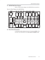
2.1 Board Description
The two circuit boards in the kit are identical. Each unit has a TRF6903 RF
transceiver and a MSP430F449 microcontroller. Each board is capable of
sending and receiving half-duplex wireless data on the European and North
American/US ISM bands. The microcontroller firmware is configured to use
the 902-MHz to 928-MHz ISM frequency band. Figure 2−1 shows top side and
back side views of the circuit board.
Figure 2−1. Top Side, Back Side of the Demonstration Board
1
13
2
3
12
11
14
2-2
3
4
10
15
16
5
9
8
6
7
Operation
Circuit board features:
1) On/Off switch
2) Battery holder for two AAA batteries in series (batteries not included)
3) Headers used to access the MSP430F449 I/O ports
4) TRF6903 RF transceiver
5) Antenna jumper (0-Ω resistor) used to select either the SMA connector or
PCB antenna (selecting both not recommended).
6) On board PCB antenna (default configuration). The antenna has modest
gain and radiates in the direction of the bend in the long arm.
7) SMA connector footprint for an external antenna or test equipment (SMA
connector not included).
8) 4-bit DIP switch used in the link demonstration mode to change the transmit/receive frequencies. The switch is connected to MSP430 I/O ports
P3.0, P3.1, P3.2, and P3.3.
9) Receive signal strength indicator (RSSI) LEDs, connected to MSP430 I/O
ports P6.0 through P6.3.
10) Four buttons used for the demonstration game application, connected to
MSP430 I/O ports P1.0 through P1.3.
11) Four LEDs used for the demonstration game application, connected to
MSP430 I/O ports P1.3 through P1.7.
12) RS−232C connector
13) JTAG connector
14) TRF6903 I/O header used to monitor or control the TRF6903.
15) 0-Ω resistor R42, remove to disable the MSP430F449 (or short reset to
ground at JTAG connector).
16) MSP430F449 microcontroller
2.2 Operation
A simple game is implemented in the firmware to demonstrate bidirectional RF
communication. The first user starts the game by pushing any sequence of
four colored buttons. The second user on the receive side responds by
pushing the same button sequence; after this response, the initial transmitter’s
board illuminates one of three LEDs depending on the information provided
by the receiving board:
- Successful user response and communication: the green LED illuminates
if the packet was delivered to the receiving board and the user on the receiving board pressed the correct sequence of buttons.
- Successful communication and user error: the orange LED illuminates if
the packet was delivered to the receiving board and the user on the
receiving board pressed the incorrect sequence of buttons.
- Communication error: the red LED illuminates if there was a communica-
tion error.
Demonstrating a Wireless Link
2-3
Operation
2.2.1
Preparing for Operation
Before you start operating the units as a demonstration make sure that you
have done the following:
- Slide the on/off switch to ON
- Place two AAA batteries on each demonstration board
- Have the same 4-bit DIP switch (SW1) configuration on both boards
Table 2−1 shows the transmit frequencies selected with the 4-bit DIP switch
(SW1). Both circuit boards must have the same channel switch settings in
order for the demonstration game to operate correctly.
Table 2−1. 4-Bit DIP Switch (SW1) Settings and Transmit Frequencies
2.2.2
1234 SW1 Setting
(1 = On, 0 = Off)
TX Frequency
(MHz)
RX Frequency
(MHz)
0000
902.3988
891.6992
0001
903.218
892.5184
0010
904.4468
893.7472
0011
905.266
894.5664
0100
906.0852
895.3856
0101
907.7236
897.024
0110
909.362
898.6624
0111
910.1812
899.4816
1000
911.8196
901.12
1001
912.6388
901.9392
1010
913.458
902.7584
1011
914.2772
903.5776
1100
915.506
904.8064
1101
916.3252
905.6256
1110
917.554
906.8544
1111
918.3732
907.6736
Power Up
Slide the power switch to ON. All the LEDs should blink to indicate power up
condition. After the power-up initialization, both units go into receive mode to
monitor for any transmit activity. The RSSI indicator LED is lighted to indicate
the signal strength in the frequency channel of operation. Red indicates the
lowest signal strength and green indicates the highest.
2.2.3
Wireless Demonstration
Either board can initiate wireless communication. Here we assume that Board
A transmits the first four-button transmitted sequence and Board B receives
the first transmission.
2-4
Operation
Use Board A to start the wireless demonstration by pressing the four colored
buttons in any sequence with about 1/2 second between successive buttons.
Once the four buttons are pushed, Board A initiates the transmission, and
waits for a reply.
Once the transmission is received by Board B, the LEDs are turned on in the
same sequence as the buttons were pushed at the transmitter side.
Immediately after the last LED is displayed, the user responds by pushing the
buttons in the exact sequence that the LEDs were lighted on Board B.
If the response sequence matches, the green LED on Board A lights up. If
there are errors due to poor or lost transmission, the red LED lights up. The
orange LED lights if the user presses an incorrect sequence of buttons in
response. This concludes the basic demonstration of the two-way RF
communication.
On completion, both boards go back to receive mode to listen for a new button
sequence.
2.2.4
RSSI Indicator
The boards are equipped with a receive signal strength indicator (RSSI) that
will illustrate the signal strength on the receiver. Four levels are used to
indicate signal strength. Red is the lowest and means no signal was received,
while green indicates the highest level of signal strength. The RSSI will show
transmission activity when the other board is transmitting a data stream on the
same DIP switch configuration or when there is another external RF source
broadcasting at that channel frequency. For best results, the two boards
should be in the same plane of orientation, with the bend in the long antenna
arm pointed towards each other.
2.2.5
Error Conditions
Cycle the system power to reinitialize the hardware if you get error conditions
that persist. Error conditions are defined as lost communication, mismatch in
response sequences, or response time outs. In some cases, antenna
orientation, signal multipath, or another interfering signal can increase errors.
Demonstrating a Wireless Link
2-5
2-6
Chapter 3
#$%
This chapter explains how to operate the MSP-TRF6903-DEMO kit to prototype new applications.
Topic
Page
3.1
Connecting to the MSP430 JTAG . . . . . . . . . . . . . . . . . . . . . . . . . . . . . . . 3-2
3.2
Loading the MSP430 With Firmware . . . . . . . . . . . . . . . . . . . . . . . . . . . . 3-3
Prototyping
3-1
Connecting to the MSP430 JTAG
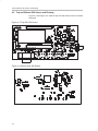
3.1 Connecting to the MSP430 JTAG
The MSP-TRF6903-DEMO is designed for rapid application development.
The MSP430 MCU flash memory can repeatedly be erased and
reprogrammed. The on-chip emulation logic allows real-time debugging and
fast code development. The MSP-TRF6903-DEMO and the MSP430 Flash
Emulation Tool provide everything that is required to develop an entire
firmware project.
For information go to http://www.msp430.com
Connector J2 provides access to the JTAG port of the MSP430 microcontroller
on the MSP-TRF6903-DEMO circuit board. The MSP-FET430 Flash
Emulation Tool (FET) interface board MSP-FETP430IF (not included in this
kit) connects to J2 and allows real-time in-system emulation. Programming the
MSP430, assembler/C source-level debugging, single stepping, multiple
hardware breakpoints, full-speed operation and peripheral access are fully
supported in-system using the JTAG connector. Figure 3−1 shows the
connections of the MSP-TRF6903-DEMO to the JTAG cable provided by the
MSP430 FET interface board.
Figure 3−1. JTAG Connector
Keyed
connector
Red stripe
3-2
Loading the MSP430 With the Firmware
3.2 Loading the MSP430 With the Firmware
The MSP−TRF6903−DEMO comes with source code installed on the MSP430
to run the demo program. The user can develop new application software that
can be downloaded to the MSP430 MCU through the JTAG connector. Since
the Compiled C code size is greater than 4kB, only unrestricted versions of the
IAR development environment (not the Kickstart version) must be used for
downloading and modifying the code.
The workspace file for compiling the demo source code
TRF6903Demo_US.eww, developed with IAR compiler version 3.20a.
is
The following steps show how to open the project file and program the
MSP430.
Step 1: Insert the two AAA batteries and slide the on/off switch to ON.
Step 2: Start the Workbench (START−>PROGRAMS−>IAR SYSTEMS−>
IAR EMBEDDED WORKBENCH.
Step 3: Use FILE−>OPEN WORKSPACE to open the workspace file at:
<Installation root>\…\ TRF6903Demo_US.eww.
Step 4: Use PROJECT−>BUILD ALL to compile and link the source code.
You can view the source code by double-clicking Common Sources,
and then double-clicking on the source files in the workspace
window.
Step 5: Ensure that the C−SPY Debugger is properly configured for the
parallel port used. (Choose PROJECT−>OPTIONS−>FET
DEBUGGER and select −>LPT1 (default) or LPT2 or LPT3 for the
parallel port configuration.)
Step 6: Use PROJECT−>DEBUG to start C−SPY. C−SPY erases the device
Flash and downloads the application object file.
Step 7: In C−SPY, use DEBUG−>GO to start the application.
Step 8: In C−SPY, use DEBUG−>STOP DEBUGGING to exit C−SPY.
Step 9: In Workbench, use FILE−>EXIT to exit Workbench.
The MSP430 is now programmed with the game demonstration code and
ready to operate.
Prototyping
3-3
3-4
Chapter 4
#& ' This chapter provides the default PCB hardware documentation in detail and
provides alternate configurations that the user may want to implement.
Topic
Page
4.1
Hardware Overview . . . . . . . . . . . . . . . . . . . . . . . . . . . . . . . . . . . . . . . . . . . 4-2
4.2
TRF6903 RF Block Diagram . . . . . . . . . . . . . . . . . . . . . . . . . . . . . . . . . . . . 4-2
4.3
MSP430F449 Block Diagram . . . . . . . . . . . . . . . . . . . . . . . . . . . . . . . . . . . 4-3
4.4
Demo Board Schematics . . . . . . . . . . . . . . . . . . . . . . . . . . . . . . . . . . . . . . 4-3
4.5
Top and Bottom Silkscreen and Drawings . . . . . . . . . . . . . . . . . . . . . . . 4-4
4.6
Parts List . . . . . . . . . . . . . . . . . . . . . . . . . . . . . . . . . . . . . . . . . . . . . . . . . . . . . 4-5
4.7
Alternate Hardware Configurations . . . . . . . . . . . . . . . . . . . . . . . . . . . . . . 47
PCB Hardware Overview
4-1
Hardware Overview
4.1 Hardware Overview
The TRF6903 ISM-band transceiver IC operates from 315 MHz to 950 MHz.
It has low power consumption and an operating voltage of 2.2 V to 3.6 V. It
features an integer-N PLL synthesizer and supports FSK and OOK operation.
Other features include on-chip clock recovery, brownout detector, and XTAL
frequency trimming in software.
The TRF6903 demonstration and development kit (MSP−TRF6903−DEMO)
provides a stand-alone demonstration of a bidirectional link using the
MSP430F449 and the TRF6903 RF transceiver.
4.2 TRF6903 RF Block Diagram
Figure 4−1 shows the block diagram of the TRF6903 ISM transceiver IC.
Figure 4−1. TRF6903 Block Diagram
LNA_IN1,
37
36
39
34
LPF amplifier
Limiter
Mixer
SLC_CAP
35
LEARN / HOLD
LPF_OUT
IF_IN1,2
44, 43
LPF_IN
MIX_OUT
47
CER_DIS
Ceramic
Discriminator
10.7-MHz Ceramic
or Discrete IF FIlter
LNA_IN2
RFIN
1, 2
LNA
Data slicer
Quadrature
demodulator
OOK
switch
RSSI
33
Bit synchronizer
and
data clock
27
41
23
Band-gap
DET_OUT
45
8
/ACounter
Brownout
detector
/N Prescaler
18
20
/Div. CTRL
6
Serial
interface
19
26
21
/BCounter
32/33
RX_DATA
DCLK
RSSI_OUT
RX_FLAG
CLOCK
DATA
STROBE
STDBY
MODE
22
Lock
detect
LOCK_DETECT
PA
PFD
CPs
VCO
VCO_TUNE
13
Loop Filter
4-2
15 CP_OUT
/Ref
2...255
32
XTAL
switch
30
XTAL_SW
4
XTAL
PA_OUT
Output
divider
1, 2, 3
31
TX_DATA
MSP430F449 Block Diagram
4.3 MSP430F449 Block Diagram
Figure 4−2 shows the block diagram of the MSP430F449 microcontroller IC.
Figure 4−2. Block Diagram of the MSP430F44x
XIN
Oscillator
XT2IN
DVCC
XOUT/TCLK
FLL+
DVSS
AVCC
AVSS
RST/NMI
ACLK
32 kB Flash
1 kB RAM
12 Bit ADC
SMCLK
48 kB Flash
2 kB RAM
8 Channels
60 kB Flash
2 kB RAM
<10 µs Conv.
XT2OUT
P5
P6
P3
I/O Port 5/6
P4
I/O Port 3/4
16 I/Os
P1
P2
I/O Port 1/2
USART0
USART1
16 I/Os, With
UART or
SPI
Function
Interrupt
Capability
MCLK
Test
MAB,
4 Bit
MAB, 16 Bit
JTAG
MCB
Incl. 16 Reg.
Emulation
Module
CPU
Bus
Conv
MDB, 16 Bit
MDB, 8 Bit
4
TMS
TCK
TDI
TDO/TDI
Multiply
MPY, MPYS
MAC,MACS
8×8 Bit
8×16 Bit
16×8 Bit
16×16 Bit
Watchdog
Timer_B7
Timer_A3
Timer
15 / 16 Bit
7 CC-Reg.
Shadow
Reg.
3 CC-Reg.
POR
SVS
Brownout
Comparator
A
Basic
Timer1
LCD
160
Segments
1,2,3,4 MUX
1 Interrupt
Vector
fLCD
4.4 Demo Board Schematics
For 6903 demo board schematics refer to the TI document SWRR001. This
document can be downloaded from the http://www.ti.com/ISMRF website.
PCB Hardware Overview
4-3
Top and Bottom Silk Screen and Drawing
4.5 Top and Bottom Silk Screen and Drawing
Figure 4−3 and Figure 4−4 show the top side and bottom side circuit board
silkscreen.
Figure 4−3. Top-Side Silk Screen
Figure 4−4. Bottom-Side Silk Screen
4-4
Parts List
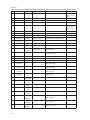
4.6 Parts List
Qty
Value
Mfg
1
0.5 pF
AVX
06035A0R5CAT2A
Capacitor, CER, 0603, 50 V, ±0.25 pF,
0.5 pF
C24
2
2.2 pF
AVX
06035A2R2CAT2A
Capacitor, CER, 0603, 50 V, ±0.25 pF,
2.2 pF
C10, 11, 14
2
22 pF
AVX
06035A220FAT2A
Capacitor, CER, 0603, 50 V, 1%,
22 pF
C8, 18
1
24 pF
AVX
06035A240FAT2A
Capacitor, CER, 0603, 50 V, 1%,
24 pF
C17
1
39 pF
AVX
06035A390FAT2A
Capacitor, CER, 0603, 50 V, 1%, 39 pF
C9, 15
3
100 pF
AVX
06035A101FAT2A
Capacitor, CER, 0603, 50 V, 1%, 100 pF
C3, 54, 63
1
75 pF
AVX
06035A750JAT2A
Capacitor, CER. 0603, 50 V, 5%, 75 pF
C20
2
82 pF
AVX
06035A820JAT2A
Capacitor, CER, 0603, 50 V, 5%, 82 pF
C5, 7
2
120 pF
AVX
06035A121JAT2A
Capacitor, CER, 0603, 50 V, 5%, 120 pF
C6, 21
1
1000 pF
AVX
06035A102JAT2A
Capacitor, CER, 0603, 50 V, 5%,
1000 pF
C39
2
5600 pF
AVX
06035A562JAT2A
Capacitor, CER, 0603, 50 V, 5%,
5600 pF
C13, 22
25
0.1 µF
AVX
0603YC104KAT2A
Capacitor, CER, 0603, 16 V, 10%,
0.1 µF
C19, 23, 30, 31,
33, 34, 37, 40,
41, 43, 44, 45,
46, 48, 49, 50,
51, 52, 53, 55,
56, 57, 58, 59,
66
4
1 µF
AVX
TAJA105K016R
Capacitor, TANT, 3216, 16 V, 10%, 1 µF
C26, 27, 28, 29
4
22 µF
CAL CHIP
GMC32Z5U226Z16NT
Capacitor, CER, 1210, 16 V, −20 +80%,
22 µF
C32, 42, 47, 60
5
RED
KingBrite
W934−IT
Diode, LED, T1, red, 12.5 MCD at
20 mA
D1, 8, 10, 11, 12
2
GRN
KingBrite
W934−GT
Diode, LED, T1, green, 12.5 MCD at
20 mA
D5, 6
2
YEL
KingBrite
W934−YT
Diode, LED, T1, yellow, 12.5 MCD at
20 mA
D2, 4
2
ORN
KingBrite
W934−??
Diode, LED, T1, orange, 12.5 MCD at
20 mA
D3, 7
2
MBRM120LT
Motorola
MBRM120LT1 or 3
Diode, Schottky, 20 PIV, 1A, DO−216AA
D9, 13
3
FMMT2222A
Central SEMI
CMPT2222A
XSTR, NPN, Gen Purp, 75 hfe,
40 Vceo, 600 mA, SOT23
Q1, 2, 3
1
10.7 MHz
Murata
SFECS10M7FA00-R0
Filter, BP, SMT, 10.7000 MHz CEN,
280 kHz, BW
FL4
1
8.2 nH
Murata
LQW1608A8N2D00
IND, SMD, 0603, ±0.5 nH, 650 mA,
8.2 nH
L5
1
9.1 nH
Murata
LQW1608A9N1D00
IND, SMD, 0603, ±0.5 nH, 650 mA,
9.1 nH
L4
LQG21N4R7K10
IND, SMD, 0805, Hi-Q, 30 mA, 4.7 µH
L1, 2
CJ10-000-T
Resistor, 0603, 5%, 0 Ω
C62, FL2, JP1,
L6, R6, 29, 41,
42, 56, 60
Resistor, 0603, 5%, 10 Ω
R32, 35, 36, 37,
38, 39, 40, 43,
44
2
4.7 µH
Murata
10
0Ω
AVX
9
10 Ω
Mfg Num
Description
Reference
PCB Hardware Overview
4-5
Parts List
Qty
Value
Mfg
21
100 Ω
Resistor, 0603, 5%, 100 Ω
R21, 22, 23, 24,
25, 26, 27, 28,
45, 46
3
200 Ω
Resistor, 0603, 5%, 200 Ω
R61, 62, 63
1
1 kΩ
Resistor, 0603, 5%, 1 kΩ
R11
1
7.5 kΩ
Resistor, 0603, 5%, 7.5 kΩ
R9
13
10 kΩ
Resistor, 0603, 5%, 10 kΩ
R13, 14, 15, 16,
17, 18, 19, 20,
33, 57, 64, 65,
66
1
15 kΩ
Resistor, 0603, 5%, 15 kΩ
R10
1
82 kΩ
Resistor, 0603, 5%, 82 kΩ
R30
1
220 kΩ
Resistor, 0603, 5%, 220 kΩ
R7
1
Header 7X2
SAMTEC
TSW−107−07−T−D
CONN, HDR, P, 14, 7X2X0.1, TTH
J2
1
Header
7x2x2mm
SAMTEC
TMM−107−01−T−D−SM
CONN, HDR, P, 14, 7×2×2 mm, SMT
J5
1
Header 3
MOLEX
22−28−4030
CONN, HDR, P, 3, 3X1X0.1, TTH
JP2
1
CONN DB−9
AMP
745781−4
CONN, PCB, DB9, F,RT
J1
1
SMA EDGE
142−0701−801
(−801=Au Plate)
CONN, Coax, SMA, Edge, SMT,
0.062 thick PCB
CO1
219−4MST
SW, Slide, 4 × SPST, 20V at
100 mA, SMT, Sealed
SW1
Johnson
Components
CTS
Mfg Num
Description
Reference
1
4 x SPST
4
PB SPST, NO
OMRON
B3W−4050 + B or S
SW, PB−SPST, NO, 50 mA, 24V, TTH
SW2, 3, 4, 5
1
EG1218
E−Switch
EG1218
SW, Slide SPDT, PCB, 30V at 0.2a
SW6
1
AS179−92
SKYWORKS
AS179−92
IC, RF switch, 1P2T, 0.1−3GHz, SC−70
SW7
1
12 mm Switch
Capacitor
OMRON
B32−1320
Capacitor, SW, 12 mm sq, fits
B3W−4050, orange
1
12 mm Switch
Capacitor
OMRON
B32−1330
Capacitor, SW, 12 mm sq. fits
B3W−4050, yellow
1
12 mm Switch
Capacitor
OMRON
B32−1350
Capacitor, SW, 12 mm sq. fits
B3W−4050, green
1
12 mm Switch
Capacitor
OMRON
B32−1380
Capacitor, SW, 12 mm sq. fits
B3W−4050, red
1
2468
Mem
ProtectionDev
BC2AAAPC
Battery holder, 2 X AAA, PCB mount
BAT1
1
TP Red
Components
Corp
TP−105−01−02
Test Point, red, 0.037 TTH
TP2
3
TP Green
Components
Corp
TP−105−01−05
Test Point, green, 0.037 TTH
TP1, 3, 5
1
TP White
Components
Corp
TP−105−01−09
Test Point, white, 0.037 TTH
TP4
1
TRF6903PT
Texas
TRF6903PG2.0
IC, RF XCVR, 315−930 MHZ, FQFP48
U1
1
MSP430F449
MSP430F449IPZ
IC, MicroP ,MixSig, 16 Bit RISC, 32kb
Flash, FQFP100
U6
0
TPS76330DBV
TPS76330DBVT
IC, PS LDO Regulator, 3 V at
150 mA, SOT32−5
U3
MAX3232CD
IC, RS232 Driver, 2 Driver,
2 Receiver, SOIC16
U4
Instruments
Texas
Instruments
Texas
Instruments
1
4-6
MAX3232−SOIC
16
Texas
Instruments
Alternate Hardware Configurations
Qty
Value
Mfg
1
NC7SZ04P5X
Fairchild
1
10.7 MHz
Murata
1
19.6608 MHz
CRYSTEK
Corp
1
32.768 kHz
Seiko
Mfg Num
Description
Reference
NC7SZ04P5X
IC, INV, Single Gate, SO70−5
U7
CDSCB10M7GA119-R0
CER Discriminator, SMT,
10.7 MHz
Y7
017119
XTAL, SMT, 19.6608 MHz, LCC−5X7
Y2
628−SPT1A−0368
XTAL, SMT, 32.768 kHz, CM202
Y4
4.7 Alternate Hardware Configurations
The MSP-TRF6903-DEMO kit is preconfigured to function under the following
assumptions:
- North American ISM frequency band, 902−928 MHz
- NRZ (non-return to zero) coding
- FSK (frequency shift keying)
- 38.4K bps
- On-board PCB antenna
The kit can be reconfigured to a limited extent. These options are covered in
this section.
4.7.1
European ISM Frequency Band
The European 868-MHz to 870-MHz ISM band is not covered in the
preconfigured system, but it can be modified by changing software variables;
download new software configurations through the JTAG connector. No
hardware changes are needed, but the antenna matching is not optimized for
this band. Go to www.ti.com/ismrf for more information.
4.7.2
External Antenna
Significant range performance may be achieved when an external antenna is
used. The actual performance improvement depends on the antenna design
and proper impedance matching. A solder pad for a SMA connector is
provided on the circuit board. The antenna can be mounted onto the SMA
connector. Jumper (JP1) setting must be moved to connect the external
antenna to the rest of the RF front end. Shorting pins 2 and 3 of JP1 with a 0-Ω
resistor connects the circuit board antenna. To connect an external antenna,
open pins 2 and 3 and short pins 1 and 2 with a 0-Ω resistor. Figure 4−5 shows
the pin-out configuration at the silk screen. Table 4−1 lists information for some
antenna suppliers. If the PCB antenna is not used, leave it unconnected,
remove the matching components from each end, and substitute one 100-Ω
resistor at each end; this prevents unwanted coupling between the PCB
antenna and the RF signal.
PCB Hardware Overview
4-7
Alternate Hardware Configurations
Figure 4−5. JP1 Pin-Out Configuration
2
3
1
Table 4−1. Antenna Suppliers
Supplier
4.7.3
Web Site
Part Number
ISM Band
Nearson
www.nearson.com
S467AM−915S
US
European
MaxRad
www.maxrad.com
MEXR902SM
US
Mobilemark
www.mobilemark.com
PSWN3−925S
US
European
W. Badland Ltd.
www.badland.co.uk
Various models
US/European
Radiall/Larsen
www.radialllarsen.com
Various models
US
European
RS-232C Port
The circuit board is designed for communication to the MSP430
microcontroller through the RS232 serial port. The UART driver is
implemented in firmware and is used in the RF evaluation mode.
4.7.4
On-Board LDO Voltage Regulator
In normal operation, the battery is connected directly to the circuit board power
through R31. There is a footprint for a low dropout (LDO) regulator for cases
where a higher-voltage power supply is used instead of the on-board batteries.
To add a LDO regulator, remove R31 and install Texas Instruments regulator
TPS76330DBV at the U3 footprint.
4.7.5
High-Frequency Crystal
The board has a footprint for a high-frequency (4 MHz) microprocessor crystal
(Y3) as well as the low-frequency crystal. The factory board configuration uses
the 32-kHz watch crystal (Y4). An internal frequency multiplier generates the
2.4576-MHz system clock.
4.7.6
SAW Filter
A SAW filter is typically used to band-limit the received RF signal and reduce
RF interference outside the ISM band. The SAW filter from Murata
(SAFC915MA70N-TC11) gives a pass band typical of 902 MHz to 928 MHz,
while providing about 30-dB attenuation in the stop band. Insertion loss in the
4-8
Alternate Hardware Configurations
pass band is about 4.5 dB. This causes a corresponding loss in operational
range due to signal attenuation. The SAW filter is not normally installed at the
factory in order to maximize range rather than noise immunity. There are other
hardware configurations for attenuating transmitter harmonics and filtering
out-of-band received noise.
4.7.7
Disabling the MSP430
In normal operation, the MSP430 microprocessor controls the TRF6903
transceiver and the game user interface. The RF section can also be
controlled directly with external computer software. To disable the
microcontroller, either short the MSP430 reset pin (RST) to ground at the JTAG
connector (preferred method), or remove R42, which disables the voltage
supply to the MSP430. The TRF6903 can then be controlled directly through
J5, the 14-pin surface-mount header.
4.7.8
Game and RF Operational Modes (Jumper JP2)
The circuit board comes with jumper JP2 set in the position for the game
(demonstration link) mode, where two circuit boards communicate with each
other in game mode to demonstrate a wireless link. In the other jumper position
(RF evaluation mode), the TRF6903 is controlled from external software run
on a PC and the commands are passed through the MSP430.
PCB Hardware Overview
4-9
4-10
Chapter 5
() This chapter describes the link demonstration firmware that has been flashed
to the microcontroller and external control software for RF test and evaluation.
Topic
Page
5.1
Software Description . . . . . . . . . . . . . . . . . . . . . . . . . . . . . . . . . . . . . . . . . . 5-2
5.2
Flowchart . . . . . . . . . . . . . . . . . . . . . . . . . . . . . . . . . . . . . . . . . . . . . . . . . . . . 5-2
5.3
Wireless Protocol Architecture . . . . . . . . . . . . . . . . . . . . . . . . . . . . . . . . . 5-3
5.4
TRF6903 Registers . . . . . . . . . . . . . . . . . . . . . . . . . . . . . . . . . . . . . . . . . . . . 5-4
5.5
Wireless Subroutines . . . . . . . . . . . . . . . . . . . . . . . . . . . . . . . . . . . . . . . . . 5-5
5.6
External Control Software for RF Evaluation Mode . . . . . . . . . . . . . . . 5-7
5.7
Operation of the Evaluation Kit in the European ISM Band . . . . . . 5-10
Software Overview
5-1
Software Description
5.1 Software Description
The demonstration software implements a simple two-way game application
utilizing a half-duplex bidirectional wireless link. Each board comes with
identical software. The software was developed using IAR’s Embedded
Workbench, version 1.26a (www.iar.com). The software files are:
- trf6903.prj – Project file
- trf6903_main.c – Main body of the program written in C language. All
subroutines are called from this program
- trf6903.s43 – Assembly subroutine to configure the TRF6903 registers
- radio03.s43 – Assembly subroutines that execute wireless transmission
and reception commands
If a newer version of the IAR compiler (Version 2.21B) is used for development,
the old project file (.prj) needs to be converted to a workspace project file
(.ewp). The conversion is one-way (not reversible). See the guide to run demo
software on newer version (2.12B) of IAR compilers (SLWA029.pdf) for more
detailed information.
5.2 Flowchart
After power up initialization, the controller is configured as a state machine to
run the link demonstration. Figure 5−1 illustrates the state machine flowchart.
Buttons and timer functions are handled through interrupt subroutines.
Figure 5−1. Game Application Flow Chart
Power
Up
Initalize
Receive_Normal
Received remote button packet
Local Button Activated
LED_Remote_Que
Local_Button_Active
Turn on LED
Wait_For_Local_
Button_Response
Response to Remote button complete
Done
All 4 button pushed | 3 sec. timeout
Receiver_Wating_For
_Response
All response button | 3 sec timeout Transmit_Packet
Local Button Initiated COM
Received response packet | 5 second timed out
LED_Response
_Result
5-2
Wireless Protocol
5.3 Wireless Protocol
The wireless data communication protocol is digital FSK at 38,400 bits per
second with NRZ coding. The communication protocol used for the
demonstration board includes preamble, packet start bit, and word-sync bit as
illustrated in Figure 5−2.
Figure 5−2. Communication Protocol
Packet Start Bit
Preamble
1
0
....
1
1
Bit Width = 26 µs
1
1
Word0
Word1
.....
0
Word0 Synch Bit
0
.....
Word1 Synch Bit
The function of the preamble is to train the receive hardware to set the proper
reference voltage threshold to extract 1 and 0 data. The preamble consists of
a train of alternating ones and zeros. A longer preamble may give better
performance at a cost of more time to deliver an equivalent data packet. The
current design has a preamble 100 bits long, or 2.6 ms in duration. Shorter
lengths may be used for more time-critical applications.
5.3.1
Packet Start and Word-Sync Bits
The packet start bit and the word sync bit are used by the receive routine to
adjust microprocessor timing for sampling the incoming data stream. The
packet start bit occurs once at the beginning of the data packet to indicate the
end of the preamble and the start of data. The sync bit is used to resynchronize
the bit stream and the data sampling timer. Over time the receive timing could
shift in phase relative to transmit timing due to the small variation in component
tolerances and performance. This shows up as an error in sampled data. The
problem gets worse as the packet size increases. Resynchronization
minimizes this drift over time.
Although resynchronization can be done at byte boundaries, word boundary
resynchronization is slightly more efficient.
The data clock recovery feature can also be used to synchronize data.
5.3.2
Wireless Data Stream
The wireless data stream for the game application is implemented as follows:
- User initiates an RF transmission on Board A by pushing four buttons in
any sequence.
- User sequence is sent to Board B using the transmission data packet
described in Figure 5−3, embedded in the communication protocol
described in Figure 5−2. The transmission packet includes a header, four
bytes with the button IDs and a checksum.
Software Overview
5-3
Wireless Protocol
- Board A waits to receive an acknowledgement packet sent by the other
board. The acknowledgement (ACK) package is illustrated in Figure 5−4.
The ACK package is embedded in the protocol described in Figure 5−2.
If Board A does not get the ACK package in the preprogrammed wait
cycle, it retries up to six times.
- Note that each time that Board B receives a transmission packet, it sends
an acknowledgment back to Board A. Figure 5−4 illustrates the ACK
packet.
Figure 5−3. 6-Byte Transmission Data Packet
Header Byte
Button 1
Button 2
Button 3
Button 4
0xFE
ID Byte
ID Byte
ID Byte
ID Byte
0x06
0x06
Checksum Byte
Figure 5−4. 4-Byte ACK Packet
0x06
5.3.3
0x06
Checksum Byte
Each packet has a checksum byte at the end of the data packet (see
Figure 5−3). The checksum byte is calculated by summing the first 5 bytes of
the packet and ignoring overflow.
5.4 TRF6903 Registers
The TRF6903 has five control registers (A through E) that are initialized using
through an on-chip serial port interface (SPI). Table 5−1 shows the values
loaded into the registers by the microprocessor during demo program
initialization.
Table 5−1. TRF6903 Game Application Register Values
Register
5-4
Parameter
Value
A
PA attenuation
Mode 0
Charge Pump
Frequency Band
0 dB
Tx
0.5 mA
915 MHz
B
PA attenuation
Mode 1
Modulation
Brownout threshold
Brownout detector
0 dB
Rx
F2.2
VSK
Off
C
Reference divider
Reference frequency
48
409.6 kHz
D
Crystal Tune
Reset Signal for PFD
Crystal Switch
20.23 pF
Derived From Prescaler
Closed
E
Receive Data Mode (RXM)
Dividers D1 D2 D3
Transmit Capture select
Self Train
38.4 kbps
Set
Wireless Protocol
5.5 Wireless Subroutines
The game application uses C language functions to implement different
communication tasks that are required to receive and send data. Brief
descriptions of these subroutines follow.
5.5.1
program_TRF6903_word()
This function configures one of the five registers of the TRF6903 transceiver.
Below is a sample code on how to use this function so that you can program
all five registers.
struct REGA_BITS {
unsigned long BND:2;
unsigned long CP_Acc:2
unsigned long PI:1;
unsigned long TX_RX0:1;
unsigned long PA0:2;
unsigned long B_DIV_M0:9;
unsigned long A_DIV_M0:5;
unsigned long ADDR:2; };
union TRF_REGA{
unsigned long all;
struct REGA_BITS bit;
};
struct TRF_REG{
union TRF_REGA a;
union TRF_REGB b;
union TRF_REGC c;
union TRF_REGD d;
union TRF_REGE e;
};
void configure_trf6903(void)
{
int pointer;
P4OUT&=0xfe;
pointer=(int)f_sel;
trf6903.a.bit.B_DIV_M0=MAIN_B_T[pointer];
trf6903.a.bit.A_DIV_M0=MAIN_A_T[pointer];
program_TRF6903_word(trf6903.a.all);
trf6903.b.bit.B_DIV_M1=MAIN_B_R[pointer];
trf6903.b.bit.A_DIV_M1=MAIN_A_R[pointer];
program_TRF6903_word(trf6903.b.all);
program_TRF6903_word(trf6903.c.all);
trf6903.d.bit.XTAL_Tune = XTAL_OFFSET;
program_TRF6903_word(trf6903.d.all);
program_TRF6903_word(trf6903.e.all);
Software Overview
5-5
Wireless Protocol
5.5.2
receive_RF(unsigned char, unsigned int*)
This function is used to receive a packet of wireless data stream. Below is an
example of how it is used.
union RF_RCV_PACKET{
unsigned int w[MAXWORD];
unsigned char b[MAXBYTE];
}rcv;
int ReceiveRFWithModeSelect(unsigned int ByteCnt)
{
int error_stat;
switch(trf6903.e.bit.RXM){
case 0:
error_stat = receive_RF(ByteCnt,rcv.w);
break;
case 3:
error_stat = receive_RF_DCLK(ByteCnt,rcv.w);
break;
// Packet stream stored in rcv.w
// Packet size stored in ByteCnt
}
}
5.5.3
send_RF(unsigned int, unsigned int*)
This function is used to transmit a packet of wireless data stream. Below is an
example of how it is used.
union RF_XMIT_PACKET{
unsigned int w[MAXWORD];
unsigned char b[MAXBYTE];
}xmit;
void SendRFWithModeSelect(unsigned int ByteCnt)
{
switch(trf6903.e.bit.TXM){
case 0:
send_RF(ByteCnt,xmit.w);
break;
case 1:
send_RF_DCLK(ByteCnt,xmit.w);
break;
}
}
5-6
External Control Software for RF Evaluation Mode
5.6 External Control Software for RF Evaluation Mode
In the RF evaluation mode, the TRF6903 transceiver is controlled by external
software run on a PC rather than by the game/demo firmware installed on the
MSP430. There is no operational link in RF evaluation mode; the transceiver
is set to one operational state at a time. Jumper JP2 sets the board operation
mode to game/demo or RF evaluation.
The RF control software has a graphical user interface (GUI) for the user to
set the transceiver state for mode (transmit, receive), frequency, power, etc.
In RF mode the external software GUI controls the TRF6903 by passing
control register words through the computer COM1 serial port, RS232 driver
IC (MAX3232), and finally through the MSP430 microcontroller to the
transceiver.
Figure 5−5 shows the graphical user interface that communicates with the
circuit board through the COM1 RS232 serial port. The user must click on the
adjacent COM1 button if its caption reads Com1 Closed in order to open the
serial port. The RF evaluation GUI is written in Borland C++ Builder, version 6,
and integrates utilities from Winsoft Ltd. to write to the serial port (ComPort).
In RF evaluation mode, the serial port COM1 is used to control the TRF6903.
An example GUI setup for transmit mode is shown in Figure 5−5. Several
boxes and pick lists have to be filled out by the user before clicking the Send
All button to configure the RF transceiver. Some of the boxes will toggle state
when the cursor is placed over the box contents and double clicked (Mode
Enable).
The crystal frequency should be set to 19.6608 MHz. Set the reference divider
to 48 (enter the value and click the Set button). The crystal tune capacitance
should be set to an intermediate value like 17, 20, or 22 pF. The charge pump
current is 0.5 mA. In the Mode Enable box, A-Word should be selected for
transmit mode. The phase-frequency detector reset should be set to
Prescaler. Enter the power amp output frequency and click the Set Frequency
button; the software rounds off the output frequency to an integer multiple of
the reference frequency. The output divider (BND) should be set to 1 for the
868-MHz and 915-MHz ISM bands. The Modulation box should be set to FSK.
For initial evaluation, set TXM=0 and TXDATA to Low.
An example GUI setup for receive mode is show in Figure 5−6. Set the Mode
Enable box contents to B-Word and Receive. Set the incoming receive signal
frequency and click the Set Freq button; the LO frequency will be set to an
integer multiple of the reference frequency. The user can set the LO frequency
10.7 MHz above or below the received RF signal by clicking on the box for
high-side Injection or low-side Injection. For initial evaluation, set the data
slicer polarity to non-inverting, RXM=CLK Recovery, BRA=8, BRB=4,
BRC=16, operational mode to Learn, TWO=0, TCOUNT=7, and Demod Tune
to an intermediate value like 3 or 4. If the down-converted IF signal is shifted
high in the 10.7-MHz filter bandwidth, try setting the RXS crystal switch to
Closed during reception (and vice-versa).
The TRF6903 is capable of transmit or receive operation in both mode 0 and
mode 1 (configured by the A and B register words), but due to the hardware
Software Overview
5-7
External Control Software for RF Evaluation Mode
configuration for the transmit/receive switch, transmit must be done in mode
0 and receive in mode 1. The tx_enable and rx_enable control lines for the
switch are derived from the TRF6903 mode control line. In other hardware
designs the switch control lines can originate at the microcontroller and can
be programmed for transmit/receive in either transceiver mode, 0 (Word A) or
1 (Word B).
Other communication utilities such as HyperTerminal or Procomm can be
used in place of the external software GUI to control the TRF6903 in
pass-through mode. Set the transmission raw data rate to 38.4 kbps, 8 bits
data, no parity, 1 stop bit, no flow control, or handshake. Send the 24-bit control
words for registers A through E in ASCII hex with a leading asterisk (hex 2A)
and trailing carriage return (hex 0D), i.e. “*[A][B][C][D][E]<CR>”.
Figure 5−5. TRF6903 Graphical User Interface for RF Evaluation, Transmit Mode
5-8
External Control Software for RF Evaluation Mode
Figure 5−6. TRF6903 Graphical User Interface for RF Evaluation, Receive Mode
Software Overview
5-9
Operation of the Evaluation Kit in the European ISM Band
5.7 Operation of the Evaluation Kit in the European ISM Band
The European ISM band covers the frequency band from 868 MHz to
870 MHz. A different set of firmware needs to be downloaded to operate the
evaluation kit at the EU band. The firmware can be downloaded from the
www.ti.com/ismrf website. See the application report Operating the
TRF6903 with MSP430 Evaluation Kit in the 868-MHZ European ISM Band
(SWRA040) for detailed information on the 868-MHz EU operation mode.
5-10