1
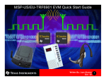
TRF6901 with MSP430 Demonstration and Development Evaluation Kit User’s Guide June 2004 Digital Radio RF Group SLWU008B IMPORTANT NOTICE Texas Instruments Incorporated and its subsidiaries (TI) reserve the right to make corrections, modifications, enhancements, improvements, and other changes to its products and services at any time and to discontinue any product or service without notice. Customers should obtain the latest relevant information before placing orders and should verify that such information is current and complete. All products are sold subject to TI’s terms and conditions of sale supplied at the time of order acknowledgment. TI warrants performance of its hardware products to the specifications applicable at the time of sale in accordance with TI’s standard warranty. Testing and other quality control techniques are used to the extent TI deems necessary to support this warranty. Except where mandated by government requirements, testing of all parameters of each product is not necessarily performed. TI assumes no liability for applications assistance or customer product design. Customers are responsible for their products and applications using TI components. To minimize the risks associated with customer products and applications, customers should provide adequate design and operating safeguards. TI does not warrant or represent that any license, either express or implied, is granted under any TI patent right, copyright, mask work right, or other TI intellectual property right relating to any combination, machine, or process in which TI products or services are used. Information published by TI regarding third-party products or services does not constitute a license from TI to use such products or services or a warranty or endorsement thereof. Use of such information may require a license from a third party under the patents or other intellectual property of the third party, or a license from TI under the patents or other intellectual property of TI. Reproduction of information in TI data books or data sheets is permissible only if reproduction is without alteration and is accompanied by all associated warranties, conditions, limitations, and notices. Reproduction of this information with alteration is an unfair and deceptive business practice. TI is not responsible or liable for such altered documentation. Resale of TI products or services with statements different from or beyond the parameters stated by TI for that product or service voids all express and any implied warranties for the associated TI product or service and is an unfair and deceptive business practice. TI is not responsible or liable for any such statements. Following are URLs where you can obtain information on other Texas Instruments products and application solutions: Products Amplifiers Applications amplifier.ti.com Audio www.ti.com/audio Data Converters dataconverter.ti.com Automotive www.ti.com/automotive DSP dsp.ti.com Broadband www.ti.com/broadband Interface interface.ti.com Digital Control www.ti.com/digitalcontrol Logic logic.ti.com Military www.ti.com/military Power Mgmt power.ti.com Optical Networking www.ti.com/opticalnetwork Microcontrollers microcontroller.ti.com Security www.ti.com/security Telephony www.ti.com/telephony Video & Imaging www.ti.com/video Wireless www.ti.com/wireless Mailing Address: Texas Instruments Post Office Box 655303 Dallas, Texas 75265 Copyright 2004, Texas Instruments Incorporated Preface Read This First About This Manual This document presents the contents of the TRF6901 demonstration and development tool kit. The user’s manual provides a thorough understanding on how to operate the MSP-TRF6901-DEMO kit and provides a detailed description of its hardware and software. Some level of product understanding regarding the MSP430F449 and the TRF6901 is required to obtain the full benefit of this user’s guide. How to Use This Manual Different topics covered in this manual may require different levels of expertise. If this is the first time you are using the MSP-TRF6901-DEMO kit, you should start with the first three Chapters. Chapter 1, TRF6901 Demonstration and Development Kit Overview, provides a general overview of the kit. Chapter 2, Demonstrating, and Chapter 3, Prototyping are focused on how to operate the kit. If your ultimate goal is to prototype with this kit, you should then review, in detail, Chapter 4, PCB Hardware Overview and Chapter 5, Software Overview, to get an understanding on how the wireless bidirectional link demonstration works. These two chapters cover hardware and software ideas that you may require some additional level of expertise. Notational Conventions ACK Acknowledgement packet JTAG Scan-based embedded system emulation MSP-TRF6901-DEMO TRF6901 demonstration and development kit RF Radio frequency RSSI Receive signal strength indicator Information About Cautions and Warnings This book may contain cautions and warnings. iii Related Documentation From Texas Instruments This is an example of a caution statement. CAUTION A caution statement describes a situation that could potentially damage your software or equipment. This is an example of a warning statement. WARNING A warning statement describes a situation that could potentially cause harm to you. The information in a caution or a warning is provided for your protection. Please read each caution and warning carefully. Related Documentation From Texas Instruments Other related documents that may be helpful are: ❏ TRF6901 datasheet - http://focus.ti.com/lit/ds/symlink/trf6901.pdf ❏ MSP430F449 data sheet http://focus.ti.com/lit/ds/symlink/msp430f449.pdf ❏ TRF6901 design guide - http://focus.ti.com/lit/an/swra035/swra035.pdf ❏ TRF6901 FAQ - http://focus.ti.com/lit/misc/slad008/slad008.pdf If You Need Assistance For more design and product information related to the TRF6901 and the MSP430 go to the following two web sites: iv ❏ http://www.msp430.com ❏ http://www.ti.com/ismrf FCC Warning This equipment is intended for use in a laboratory test environment only. It generates, uses, and can radiate radio frequency energy and has not been tested for compliance with the limits of computing devices pursuant to subpart J of part 15 of FCC rules, which are designed to provide reasonable protection against radio frequency interference. Operation of this equipment in other environments may cause interference with radio communications, in which case the user at their own expense will be required to take whatever measures may be required to correct this interference. Disclaimer Please note that the enclosed demonstration boards are experimental printed circuit boards and are therefore only intended for device evaluation We would like to draw your attention to the fact that these boards have been processed through one or more of Texas Instruments’ external subcontractors which have not been production qualified. Device parameters measured, using these boards, are not representative of any final data sheet or of a final production version. Texas Instruments does not represent or guarantee that a final version will be made available after device evaluation. THE DEMONSTRATION BOARDS ARE SUPPLIED WITHOUT WARRANTY OF ANY KIND, EXPRESSED, IMPLIED OR STATUATORY, INCLUDING BUT NOT LIMITED TO, ANY IMPLIED WARRANTY OF MERCHANTABILITY OR FITNESS FOR A PARTICULAR PURPOSE TEXAS INSTRUMENTS ACCEPTS NO LIABILITY WHATSOEVER ARISING AS A RESULT OF THE USE OF THESE BOARDS. The fee associated with the demonstration boards is a partial nonrecurring engineering fee (NRE) to partially defray the engineering costs associated with the board development and applications support for the RF integrated semiconductor product. The demonstration board is a tool for demonstrating and evaluating the RF semiconductors supplied by Texas Instruments. The demonstration board is supplied to prospect component customers to provide services and software allowing the prospect customers to evaluate the RF semiconductors in products they would build. The demonstration board may be operated only for product demonstration or evaluation purposes and then only in nonresidential areas. Texas Instruments understanding is that the customers’ products using the RF parts listed shall be designed to comply with all applicable FCC and appropriate regulatory agency requirements and will, upon testing, comply with these requirements. Operation of this device is subject to the conditions that it does not cause harmful interference and that it must accept any interference. Contents 1 2 TRF6901 Demonstration and Development Kit Overview ...................................1-1 1.1 Description.........................................................................................................1-2 1.2 Contents ............................................................................................................1-2 1.3 Equipment Requirement....................................................................................1-2 Demonstrating .........................................................................................................2-1 2.1 Board Description ..............................................................................................2-2 2.2 Operation...........................................................................................................2-3 2.2.1 2.2.2 2.2.3 2.2.4 2.2.5 3 4 Prototyping ..............................................................................................................3-1 3.1 Connections to the MSP430 JTAG ....................................................................3-2 3.2 Loading the MSP430 With the Firmware...........................................................3-2 PCB Hardware Overview ........................................................................................4-1 4.1 Hardware Overview ...........................................................................................4-2 4.2 TRF6901 RF Block Diagram .............................................................................4-2 4.3 MSP430F449 Block Diagram ............................................................................4-2 4.4 Demo Board Schematics...................................................................................4-3 4.5 Top and Bottom Silk Screen and Drawing.........................................................4-3 4.6 Parts List............................................................................................................4-5 4.7 Alternate Hardware Configurations ...................................................................4-6 4.7.1 4.7.2 4.7.3 4.7.4 4.7.5 4.7.6 4.7.7 5 Getting Ready .................................................................................................... 2-4 Power Up ........................................................................................................... 2-4 Wireless Demonstration..................................................................................... 2-5 RSSI Indicator.................................................................................................... 2-5 Error Conditions ................................................................................................. 2-5 European ISM-Band .......................................................................................... 4-6 External Antenna ............................................................................................... 4-6 RS-232C Port..................................................................................................... 4-7 On-Board LDO Regulator .................................................................................. 4-7 High-Frequency Cystal ...................................................................................... 4-7 SAW Filter ..........................................................................................................4-7 MSP430 Disable ................................................................................................ 4-8 Software Overview ..................................................................................................5-1 5.1 Software Description .........................................................................................5-2 5.2 Flowchart ...........................................................................................................5-2 5.3 Wireless Protocol Architecture ..........................................................................5-3 5.3.1 5.3.2 5.3.3 5.3.4 Preamble............................................................................................................ 5-3 Packet Start and Word-Synch-Bits .................................................................... 5-3 Wireless Data Stream ........................................................................................ 5-3 Checksum Byte.................................................................................................. 5-4 5.4 TRF6901 Registers ...........................................................................................5-4 5.5 Wireless Subroutines.........................................................................................5-5 5.5.1 5.5.2 5.5.3 program_trf69() .................................................................................................. 5-5 receive_RF(unsigned char, unsigned int*)......................................................... 5-6 send_RF(unsigned int, unsigned int*)................................................................ 5-6 vi Figures 2-1. Top-Side and Back-Side Picture of the Demonstration Board ............................ 2-2 3-1. JTAG Connector ...................................................................................................... 3-2 4-1. TRF6901 Block Diagram.......................................................................................... 4-2 4-2. Block Diagram of the MSP430F44x........................................................................ 4-3 4-3. Top-Side Silk Screen ............................................................................................... 4-3 4-4. Bottom-Side Silk Screen ......................................................................................... 4-4 4-5. JP1 Pin-Out Configuration...................................................................................... 4-7 5-1. Game Application State Machine Architecture ..................................................... 5-2 5-2. Communication Protocol ........................................................................................ 5-3 5-3. 6-Byte Transmission Data Packet .......................................................................... 5-4 5-4. 4-Byte ACK Packet .................................................................................................. 5-4 Tables 2-1. 4-bit DIP Switch (SW1) Frequency Configuration................................................. 2-4 4-1. Antenna Suppliers ................................................................................................... 4-7 5-1. TRF6901 Game Application Register Values ........................................................ 5-5 vii Chapter 1 TRF6901 Demonstration and Development Kit Overview This chapter provides an overview of the TRF6901 demonstration and development kit. Topic Page 1.1 Description.................................................................................................1-2 1.2 Contents.....................................................................................................1-2 1.3 Equipment Requirements .........................................................................1-2 1-1 TRF6901 Demonstration and Development Kit Overview 1.1 Description The MSP-TRF6901-DEMO kit is used to demonstrate a bidirectional RF (radio frequency) link without the need of a personal computer and to prototype by downloading new software code to the MSP430F449 using a JTAG connector. The schematics and layout of the board can be used as a reference design if desired, limited by the software system parameters provided for the demonstration. 1.2 Contents Contained within the TRF6901 demonstration and development kit are the following: ❏ Two TRF6901 demonstration boards ❏ This user’s guide Software code is not included in the kit. Software and hardware documentation related to this kit can be downloaded at: http://www.ti.com/ismrf 1.3 Equipment Requirement The following equipment is not included in this kit and is required to operate the MSP-TRF6901-DEMO kit: 1-2 ❏ Four (4) AAA batteries ❏ MSP430 bus expansion cable for the JTAG connector, required only for prototyping purposes Chapter 2 Demonstrating This chapter explains how to operate the MSP-TRF6901-DEMO kit to demonstrate a RF bidirectional link Topic Page 2.1 Board Description .....................................................................................2-2 2.2 Operation ...................................................................................................2-3 2-1 Demonstrating 2.1 Board Description The two boards that you have received with your kit are identical. Each unit has a TRF6901 single-IC RF transceiver and a MSP430F449 microcontroller. Each board is capable of sending and receiving half-duplex wireless data on the European and US ISM bands. The boards are preconfigured to use the 902 to 928 MHz ISM band out of the box. Figure 2-1 shows a top-side and back-side picture of each board. Figure 2-1. Top-Side and Back-Side Picture of the Demonstration Board 2-2 Demonstrating Each board features the following functions: a) On/Off switch b) Battery holder: stores two AAA batteries in series (batteries are not included) c) MSP430 headers: used to access the I/O ports of the MSP430F449 d) TRF6901 component e) Antenna selection jumper used to select either the SMA connector or PCB antenna. f) On board PCB antenna (default configuration) g) SMA footprint connector used to add an external antenna (SMA connector not included) h) 4-bit DIP switch used in the demonstration to change the frequency configuration. The MSP430 I/O ports P2.3, P2.6, P2.7, and P3.0 connect to the 4-bit DIP switch. i) Receive signal strength indicator (RSSI) LEDs – used as the RSSI for the demonstration. The LEDs are tied to the MSP430 P6.0 to P6.3 I/O ports. j) Four buttons used for the demonstration application; connected to the MSP430 P1.0 to P1.3 I/O ports. k) Four LEDs used for the demonstration application; connected to the MSP430 P1.3 to P1.7 I/O ports. l) RS-232C connector footprint (RS-232C circuitry is not included in the kit) m) JTAG connector n) TRF6901 I/O header used to control or monitor the TRF6901 component externally. o) MSP430 disable jumper used to disable the MSP430F449 component p) MSP430F449 component 2.2 Operation A simple game is implemented in the firmware to demonstrate bidirectional RF communication. The transmit side initiates the game by pushing any sequence of four buttons. The user on the receive side responds by pushing the same button sequence. After a complete roundtrip, the transmit side illuminates one of three LEDs depending on the feedback provided by the receiving board: ❏ Successful user response and communication. The green LED illuminates if the packet was delivered to the receiving board and the user on the receiving board pressed the correct sequence of buttons. ❏ Successful communication and user error. The orange LED illuminates if the packet was delivered to the receiving board and the user on the receiving board pressed the incorrect sequence of buttons. ❏ Communication error. The red LED illuminates if there was a communication error. 2-3 Demonstrating 2.2.1 Getting Ready Before you start operating the units as a demonstration make sure that you have done the following: ❏ Slide the on/off switch to off ❏ Place two AAA batteries on each demonstration board ❏ Have the same 4-bit DIP switch (SW1) configuration on both boards See Table 2-1 for a list of the US ISM band frequencies supported using the 4-bit DIP switch (SW1). It does not matter what 4-bit DIP switch setting you choose to operate the demo, as long as both boards have the same configuration. Table 2-1. 4-bit DIP Switch (SW1) Frequency Configuration 2.2.2 1234 SW1 setting (1=On, 0=Off) 0000 Frequency (MHz) 902 0001 903 0010 904 0011 905 0100 906 0101 907 0110 908 0111 909 1000 910 1001 911 1010 912 1011 913 1100 914 1101 915 1110 916 1111 917 Power Up Slide the power switch to ON. All the LEDs should blink to indicate power up condition. After the power up initialization, both units go into receive mode to monitor for any activities. The RSSI indicator LED is lit up to indicate the signal strength in the frequency of operation. Red indicates the lowest signal strength while green indicates the highest. 2-4 Demonstrating 2.2.3 Wireless Demonstration Either board can initiate a wireless communication. For explanation purposes, call Board-A the board that you use to transmit the first fourbutton sequence and Board-B the board that you are using to receive the first four-button transmission. Use Board-A to start the wireless demonstration by pressing any sequence of four buttons with about 1/2 second in between. Once the four buttons are pushed, Board-A initiates the transmission, and waits for a reply. Once the transmission is received by Board-B, the LEDs are turned on in the same sequence as the buttons were pushed at the transmitter side. Immediately after the last LED is displayed, respond by pushing the buttons in the exact sequence that the LED is displayed on Board-B. If the response sequence matches, the green LED on Board A lights up. If there are errors due to bad transmission, lost transmission, or not matching response sequence, the red LED lights up. This completes the round trip RF communication demonstration. On completion, both boards go back to listen mode to accept a new sequence. 2.2.4 RSSI Indicator The boards are equipped with a receive signal strength indicator that will illustrate the signal strength on the receiver. 4 levels are used to indicate signal strength. Red is the lowest and means no signal received at all, while green indicates the highest level of signal strength. The RSSI will show transmission activity when the other board is transmitting a data stream on the same DIP switch configuration or there is another external source interfering with that channel. 2.2.5 Error Conditions Cycle power the system to reinitialize the hardware if you get error conditions that persist. Error conditions are defined as lost communication, mismatch in response sequences, or response time outs. 2-5 Chapter 3 Prototyping This chapter explains how to operate the MSP-TRF6901-DEMO kit to prototype new applications Topic Page 3.1 Connecting to the MSP430 JTAG.............................................................3-2 3.2 Loading the MSP430 With the Firmware .................................................3-2 3-1 Prototyping 3.1 Connecting to the MSP430 JTAG The MSP-TRF6901-DEMO is designed for rapid application development. This is made possible by the MSP430 MCU with flash memory that can be erased and programmed several times. Additionally, the on-chip emulation logic allows real-time debugging and fast code development. BEFORE CONNECTING TO THE MSP430 JTAG, THE 2 AAA BATTERIES MUST BE REMOVED OR THE ON-OFF SWITCH MUST BE IN THE OFF POSITION. Connector J2 provides access to the JTAG port of the MSP430 device in the MSP-TRF6901-DEMO kit. The MSP-FET430 flash emulation tool interface board MSP-FETP430IF (not included in this kit) connects to J2 and allows real-time in-system emulation. Programming the MSP430, assembler/ C-source level debug, single stepping, multiple hardware breakpoints, full-speed operation and peripheral access are fully supported in-system using the JTAG. The MSP-TRF6901-DEMO and the MSP430 Flash Emulation Tool (FET) provide everything that is required to develop an entire project. Figure 3-1 shows the connections of the MSP-TRF6901DEMO to the JTAG cable provided by the MSP430 FET interface board. Figure -3-1. JTAG Connector Dented Side Red 3.2 Loading the MSP430 With the Firmware The MSP-TRF6901-DEMO comes with complete source code to program the MSP430 to run the demo program. The user can develop new application software that can be downloaded to the MSP430 MCU using the JTAG connector. For practical purposes, the following procedure illustrates how to download the demo source code to the MSP430. The project file for compiling the demo source code is trf6901_demo.prj. The following steps show how to open this project and program the MSP430: 3-2 Prototyping Step 1. Remove the two AAA batteries or slide the On/Off switch to Off. Step 2. Start the Workbench (START->PROGRAMS->IAR SYSTEMS>IAR EMBEDDED WORKBENCH. Step 3. Use FILE->OPEN to open the project file at: root>\…\ trf6901_demo.prj. <Installation Step 4. Use PROJECT->BUILD ALL to compile and link the source code. You can view the source code by double-clicking Common Sources, and then double-clicking on the source files in the trf6901_demo.prj window. Step 5. Ensure that C-SPY is properly configured (With DEBUG selected, PROJECT->OPTIONS->C-SPY); 1. PARALLEL PORT>PARALLEL PORT->LPT1 (default) or LPT2 or LPT3 Step 6. Use PROJECT->DEBUGGER to start C-SPY. C-SPY erases the device Flash, and then download to the device Flash the application object file. Step 7. In C-SPY, use EXECUTE->GO to start the application. Step 8. In C-SPY, use FILE->EXIT to exit C-SPY. Step 9. In the Workbench, use FILE->EXIT to exit the Workbench. The MSP430 is now programmed with the demo code and ready to operate. 3-3 Chapter 4 PCB Hardware Overview This chapter provides the default PCB hardware documentation in detail and provides alternate configurations that the user may want to implement. Topic Page 4.1 Hardware Overview ...................................................................................4-2 4.2TRF6901 RF Block Diagram.......................................................................4-2 4.3 MSP430F449 Block Diagram ....................................................................4-2 4.4 Demo Board Schematics ..........................................................................4-3 4.5 Top and Bottom Silkscreen and Drawings..............................................4-3 4.6 Parts List ....................................................................................................4-5 4.7 Alternate Hardware Configurations .........................................................4-6 4-1 PCB Hardware Overview 4.1 Hardware Overview The TRF6901 ISM-band transceiver IC operates from 860 MHz to 930 MHz. It has low power consumption and an operating voltage of 1.8 V to 3.6 V. It uses an integer-N synthesizer and supports FSK operation. Other features include an on-chip reference oscillator, phase lock loop, brownout detector, and XTAL software trimming. The TRF6901 demonstration and development kit (MSP-TRF6901-DEMO) provides a stand alone demonstration of a bidirectional link using the MSP430F449 and the TRF6901 4.2 TRF6901 RF Block Diagram Figure 4-1 shows the block diagram of the TRF6901 ISM transceiver IC. Figure 4-1. TRF6901 Block Diagram 4.3 MSP430F449 Block Diagram Figure 4-2 shows the block diagram of the MSP430F449 microcontroller IC. 4-2 PCB Hardware Overview Figure 4-2. Block Diagram of the MSP430F44x 4.4 Demo Board Schematics All the schematics for the demonstration boards can be found at http://www-s.ti.com/sc/techzip/slwc036.zip. 4.5 Top and Bottom Silk Screen and Drawing Figure 4-3 shows the top-side silkscreen of the demo board and Figure 4-4 shows the bottom-side silkscreen. Figure 4-3. Top-Side Silk Screen 4-3 PCB Hardware Overview Figure 4-4. Bottom-Side Silk Screen 4-4 PCB Hardware Overview 4.6 Parts List Item Qty Value Source Part Number MEMORY PROTECTION DEVICES BC2AAAPC Description Reference 1 1 2 1 3 4 5 1 2 3 4.7pF 82pF 15pF AVX AVX AVX 06035A4R7CAT2A 06035A820JAT2A 06035A150GAT2A BATTERY HOLDER, 2 X AAA, PCB MOUNT CONN, COAX, SMA, EDGE, SMT, 0.062THK PCB CAP, CER, 0603, 50V, +/-.25PF, 4.7PF CAP, CER, 0603, 50V, 5%, 82PF CAP, CER, 0603, 50V, 2%, 15PF 6 7 1 2 120pF 68pF AVX AVX 06035A121JAT2A 06035A680JAT2A CAP, CER, 0603, 50V, 5%, 120PF C6 CAP, CER, 0603, 50V, 5%, 68PF C7,C17 8 1 22pF AVX 06035A220FAT2A 9 2 2.7pF AVX 06035A2R7CAT2A CAP, CER, 0603, 50V, 1% , 22PF C9 CAP, CER, 0603, 50V, +/-.25PF, 2.7PF C11,C10 10 2 100pF AVX 06035A101FAT2A 11 1 2200pF AVX 06035A222JAT2A 12 1 2.2pF AVX 06035A2R2CAT2A 13 1 150pF AVX 06035A151FAT2A 14 3 1000pF AVX 15 BAT 2 CELL 24 .1uF AVX 16 1 .01uF AVX 17 1 0.5pF AVX 18 4 1.0uF KEMET 19 4 22uF CAL CHIP 20 2 10pF AVX 21 2 RED LITEON 22 2 YEL LITEON 23 2 ORN LITEON 24 2 GRN LITEON 25 1 MBRM120LT3 MOTOROLA 26 1 SFECV10.7MS2S-A MURATA 27 28 1 1 47nH HEADER 7X2 MURATA SAMTEC 29 2 4.7uH MURATA 30 1 8.2nH MURATA 31 1 10nH MURATA 32 33 34 1 6 1 6.8nH 0 220K MURATA AVX 35 36 37 38 9 1 1 1 10K 6.8K 18K 1K 39 40 8 1 100 82K BAT1 CO1 C2 C3,C5 C18,C4,C8 CAP, CER, 0603, 50V, 1%, 100PF C20,C54 CAP, CER, 0603, 50V, 5%, 2200PF C13 CAP, CER, 0603, 50V, +/-.25PF, 2.2PF C14 CAP, CER, 0603, 50V, 1%, 150PF C15 CAP, CER, 0603, 50V, 5%, 06035A102JAT2A 1000PF C16,C21,C39 C19,C23,C30,C31,C33,C34,C 37,C40,C41,C43,C44,C45,C4 6,C48,C49,C50,C51,C52,C53, CAP, CER, 0603, 16V, 10%, C55,C56,C57,C58,C59 0603YC104KAT2A 0.1UF CAP, CER, 0603, 50V, 10%, 06035C103KAT2A 0.01UF C22 CAP, CER, 0603, 50V, +/-.25PF, 06035A0R5CAT2A 0.5PF C24 CAP, TANT, 3216, 16V, 10%, T491A105K016AS 1.0UF C26,C27,C28,C29 CAP, CER, 1210, 16V, -20 +80%, GMC32Z5U226Z16NT 22UF C32,C42,C47,C60 CAP, CER, 0603, 50V, +/-.5PF, 06035A100DAT2A 10PF C36,C35 DIODE, LED, T1, RED, 12.5MCD LTL-4222N @ 20MA D8,D1 DIODE, LED, T1, YEL, 12.5MCD LTL-4252N @ 20MA D2,D4 DIODE, LED, T1, ORN, 12.5MCD LTL-4296N @ 20MA D7,D3 DIODE, LED, T1, GRN, 12.5MCD LTL-4232N @ 20MA D6,D5 DIODE, SCHOTTKY, 20PIV,1A, MBRM120LT3 DO-216AA D9 SFECV10.7MS2S-A- FILTER, BP, SMT, 10.7000MHZ TC CEN, 230KHZ BW FL1 IND, SMD, 0603 +/- 2%, 380mA, LQW1608A47NG00 47nH JP1 TSW-107-07-T-D CONN, HDR, P, 14, 7X2X0.1, TTH J2 IND, SMD, 0805, 30%, 30mA, LQG21C4R7N00T1 4.7UH L2,L1 IND, SMD, 0603, +/- .5nH, 650mA, LQW1608A8N2D00 8.2nH L3 IND, SMD, 0603, +/- 2%, 650mA, LQW1608A10NG00 10nH L4 IND, SMD, 0603, +/- .5nH, ?mA, LQW1608A6N8D00 6.8nH L5 CJ10-000-T RES, 0603, 5%, 0 OHM R6,R29,R31,R34,R41,R42 RES, 0603, 5%, 220K OHM R7 R13,R14,R15,R16,R17,R18,R RES, 0603, 5%, 10K OHM 19,R20,R33 RES, 0603, 5%, 6.8K OHM R9 RES, 0603, 5%, 18K OHM R10 RES, 0603, 5%, 1K OHM R11 R21,R22,R23,R24,R25,R26, RES, 0603, 5%, 100 OHM R27, R28 RES, 0603, 5%, 82K OHM R30 4-5 PCB Hardware Overview 41 42 8 1 10 1 RES, 0603, 5%, 10 OHM RES, 0603, 5%, 1 OHM SW, DIP, 4 X SPST, 24V @ 25mA, TTH SW, PB-SPST, NO, 50MA, 24V, TTH 47 1 A6E-4104 OMRON A6E-4104 48 4 PB SPST, NO OMRON B3W-4050S 49 1 EG1218 E-SWITCH EG1218 50 1 TRF6901PT TI TRF6901PT 51 1 MSP430F449 TI 52 1 10.700MHZ MURATA MSP430F4449IPZ CDSCA10M7GA119R0 53 54 1 1 20.000MHZ 32.768KHZ CAL CRYSTAL CCL-SM7 XTAL, SMT, 20.0000MHZ, LCC4LAB 20.00000MHZ J15F 7X5MM CITIZEN CM202-32.768KDZFT XTAL, SMT, 32.768KHZ, CM202 SW, SLIDE SPDT, PCB, [email protected] IC, RF XCVR, 860-930MHZ, FQFP48 IC, MICROCONTROLLER, MIXED SIGNAL, 16-BIT RISC, 32KB FLASH, FQFP100 CER DISCRIMINATOR, SMT, 10.700MHZ, R32,R35,R36,R37,R38,R39, R43,R44 R40 SW1 SW2,SW3,SW4,SW5 SW6 U1 U6 Y1 Y2 Y4 4.7 Alternate Hardware Configurations The MSP-TRF6901-DEMO kit is preconfigured to function under the following assumptions: ❏ US ISM-band ❏ NRZ (no return to zero) ❏ FSK (frequency shift keying) ❏ 38.4K bps ❏ On-board PCB antenna The kit can cover some limited alternate configurations. These options are covered in this section. 4.7.1 European ISM-Band European 868-MHz to 870-MHz ISM-band configuration is not covered in the pre-configured system, but it can be modified by changing software variables; the JTAG can download new software configurations. No hardware changes are needed, but the antenna matching is not optimized for this band. Go to www.ti.com/ismrf for more information on this option. 4.7.2 External Antenna Significant range performance may be achieved when an external antenna is used. The actual performance improvement will depend on the antenna design and proper impedance matching. A solder pad for SMA connector is designed into the board. The antenna can be mounted onto the SMA connector. Jumper (JP1) setting must be moved to connect the external antenna to the rest of the RF front end. Shorting pins 2 and 3 of JP1 with a 0-Ω resistor connects the internal antenna. To connect the external antenna, open pins 2 and 3 and short pins 1 and 2 with a 0-Ω resistor. Figure 4-5 shows the pin-out configuration at the silk screen. Table 4-1 provides some antenna supplier information. 4-6 PCB Hardware Overview Figure 4-5. JP1 Pin-Out Configuration 2 3 1 Table 4-1. Antenna Suppliers 4.7.3 Supplier MaxRad Web Site www.maxrad.com Part number MEXR902SM ISM Band US Mobilemark www.mobilemark.com PSWN3-925S PSTNS-900S US European W. Badland Ltd. www.badland.co.uk Various models US / European Radiall/Larsen Various models SPDA24832 US European www.radialllarsen.com RS-232C Port Provisions for communicating to the on-board processor through the RS232 serial link are designed onto the board. Populate the appropriate parts shown in the schematics for the physical link, including the Texas Instruments MAX3232 component. The UART driver must be implemented in firmware. 4.7.4 On-Board LDO Regulator In normal operation, the battery voltage is directly connected to the power input to the processor through R31. Provision for LDO usage is provided in cases where higher voltage from an external supply is used instead of onboard battery. To add an LDO regulator, remove R31 and install U3 with a Texas Instruments TPS76330DBV component. The boards are shipped from factory with no installed LDO. 4.7.5 High-Frequency Crystal The board has a foot print for high-frequency crystal operation (Y3) as well as the low-frequency crystal operation. The factory default uses standard 32-kHz watch crystal (Y4) for low-frequency operation. Internal frequency multiplier is used to generate system clock frequency of 2.4576 MHz. 4.7.6 SAW filter A SAW filter is typically used to band-limit the received RF signal to reduce the interference from RF energy in the frequency band other than the ISM band. The SAW filter from Murata (SAFC915MA70N-TC11) gives a pass band typical of 902 MHz to 928 MHz, while providing about 30 dB attenuation at stop band. The part is also specified at ~4.5 dB signal loss in 4-7 PCB Hardware Overview the pass band. This translates to corresponding loss in range of operation. The SAW filter is not installed for the factory default to give optimum range rather than optimum immunity. There are other cost-effective implementations that address the same objective with lower dB signal loss. 4.7.7 MSP430 Disable In normal operation, the MSP430 on-board processor controls the TRF6901 component and the user interface. During evaluation, the RF section can be driven directly by external control signals. This can be accomplished by removing R42, which disables the voltage supply to the MSP430 processor. The TRF6901 can then be accessed directly using the TRF6901 header at J5. 4-8 Chapter 5 Software Overview This chapter describes the software flow used for the demonstration application that is preconfigured in each demonstration board. Topic Page 5.1 Software Description.................................................................................5-2 5.2 Flowchart ...................................................................................................5-2 5.3 Wireless Protocol Architecture ................................................................5-3 5.4 TRF6901 Registers ....................................................................................5-4 5.5 Wireless Subroutines................................................................................5-5 5 -1 5.1 Software Description The software implements a simple game application demonstrating a bidirectional wireless link. Each board comes with identical software. The software was developed using IAR embedded workbench (www.iar.com). Below is the software files used: ❏ trf6901_demo.prj – Project file ❏ trf6901_demo.c – main body of the program written in C languge. All the subroutines are called from this program listing ❏ trf6901.s43 – assembly subroutine that is utilized to configure the registers of the TRF6901 component ❏ radio01.s43 – assembly subroutines used to execute wireless transmission and reception commands. 5.2 Flowchart Upon power up initialization, a state machine is established to run the demonstration function. Figure 5-1 illustrates the state machine flowchart. Buttons and timer functions are handled through interrupt subroutines. Figure 5-1. Game Application State Machine Architecture Power Up Initalize Received remote button packet Receive_Normal Local Button Activated LED_Remote_Que Local_Button_Active Turn on LED Wait_For_Local_ Button_Response Response to Remote button complete All 4 button pushed | 3 sec. timeout Done Receiver_Wating_For _Response All response button | 3 sec timeout Local Button Initiated COM Transmit_Packet Received response packet | 5 second timed out LED_Response _Result 5-2 Software Overview 5.3 Wireless Protocol Architecture The wireless data communication protocol is digital FSK at 38,400 bits per second NRZ. The communication protocol used for the demonstration board includes preamble, packet start bit, and word-synch-bit as illustrated in Figure 5-2. Figure 5-2. Communication Protocol Pre-Amble 1 0 1 Bit Width = 26 us Word0 Packet Start Bit .... 1 1 1 0 Word0 Synch Bit Word1 ..... ..... 0 Word1 Synch Bit Communication Protocol Preamble The function of the preamble is to train the receive hardware to set the proper threshold to extract 1 and 0 patterns. The preamble typically consists of a train of alternating 1 and 0. A longer preamble may give better performance at a cost of more time needed to deliver the equivalent packet. For the current design, the preamble is 100 bits long, for 2.6-ms duration. Shorter length may be used for more time critical requirements. 5.3.1 Packet Start and Word-Synch-Bits The packet start bit and the word synch bit are used by the receive routine to adjust timing for sampling the incoming data bit stream. The packet start bit occurs once at the beginning of the valid data to indicate the start of the data, and end of preamble. The synch bit is used to resynchronize the bit stream and the data sampling timer. Over time the receive timing could shift in phase relative to transmit timing due to the small variation in the tolerances of the components. This shows up as an error in sampled data. The problem gets worse as the packet size increases. Resynchronization minimizes this drift over time. Although resynchronization can be done at byte boundary, word boundary resynchronization is slightly more efficient. 5.3.2 Wireless Data Stream The wireless data stream implemented for the game application was implemented as follows: ❏ User initiates an RF transmission on Board-A by pushing four buttons in any sequence ❏ User sequence is sent to Board-B using the transmission data packet described in Figure 5-3 embedded in the communication protocol described in Figure 5-2. The transmission packet includes a header, four bytes with the button IDs and a checksum 5-3 ❏ Board-A goes to a wait state, where it waits to receive an acknowledgement packet sent by the other board. The (ACK) acknowledgement package is illustrated in Figure 5-4. The ACK package is embedded in the protocol described in Figure 5-2. If BoardA does not get the ACK package in the preprogrammed waiting cycle, then it retries for up to six times ❏ Note that each time that Board-B receives a transmission packet, it acknowledges back to Board-A. Figure 5-4 illustrates the ACK packet. Figure 5-3. 6-Byte Transmission Data Packet Header Byte Button 1 Button 2 Button 3 Button 4 OxFE ID Byte ID Byte ID Byte ID Byte 0x06 0x06 0x06 Checksum Byte Figure 5-4. 4-Byte ACK Packet 0x06 5.3.3 Checksum Byte Each packet has a checksum byte at the end of the data packet (see Figure 5-3). The checksum byte is calculated by summing the first 5 bytes of the packet and ignoring the overflow. 5.4 TRF6901 Registers The TRF6901 needs to have its four (A thru D) registers initialized using the serial port interface (SPI) so that it can operate as desired. Table 5-1 shows the values used on the four registers of the TRF6901 when the program initializes. 5-4 Software Overview Table 5-1. TRF6901 Game Application Register Values Register A Parameter PA attenuation Mode 0 Charge Pump DC/DC Value 0 dB Tx 0.5 mA Off B PA attenuation Mode 1 Modulation Brownout Threshold Brownout detector 0 dB Rx FSK 1.8 V Off C Reference Divider Reference Frequency 60 333.333 kHz D Crystal Tune Reset Signal for PFD 20.23 pF Derived From Prescaler 5.5 Wireless Subroutines The game application uses C functions to address the different communication tasks required to receive and send data. Read ahead for a brief description of these subroutines. 5.5.1 program_trf69() This function configures one of the four (A thru D) registers of the TRF6901 component. Here is a sample code on how to use this function so that you can program all the four registers: struct trf69_control{ unsigned int a_word_l, a_word_h, b_word_l, b_word_h; unsigned int c_word_l, c_word_h, d_word_l, d_word_h; }trf6901; main() { unsigned long trf69; int pointer; trf69 = REGISTER_A; // REGISTER_A is a constant trf6901.a_word_h = (unsigned int) (trf69>>16); trf6901.a_word_l = (unsigned int) (trf69); program_TRF69(trf6901.a_word_h,trf6901.a_word_l); trf69 = REGISTER_B; // REGISTER_B is a constant */ trf6901.b_word_h = (unsigned int) (trf69>>16); trf6901.b_word_l = (unsigned int) (trf69); program_TRF69(trf6901.b_word_h,trf6901.b_word_l); 5-5 trf69 = REGISTER_C; // REGISTER_C is a constant */ trf6901.c_word_h = (unsigned int) (trf69>>16); trf6901.c_word_l = (unsigned int) (trf69); program_TRF69(trf6901.c_word_h,trf6901.c_word_l); trf69 = REGISTER_D; // REGISTER_D is a constant */ trf6901.d_word_h = (unsigned int) (trf69>>16); trf6901.d_word_l = (unsigned int) (trf69) program_TRF69(trf6901.d_word_h,trf6901.d_word_l); } 5.5.2 receive_RF(unsigned char, unsigned int*) This function is used to receive a packet of wireless data stream. Here is an example of how it is used: struct RF_XMIT_PACKET { int packetsize; unsigned int xmit[MAXWORD]; unsigned int rcv[MAXWORD]; }buf; Main() { int errorcode; errorcode = receive_RF(buf.packetsize,buf.rcv); // Packet stream stored in buf.rcv // Packet size stored in buf.packetsize } 5.5.3 send_RF(unsigned int, unsigned int*) This function is used to transmit a packet of wireless data stream. Here is an example on how it is used: main() { buf.xmit[1]=ACK_CODE; buf.xmit[0]=ACK_CODE; ComFlag|=rf_X_buf_full; send_RF(4,buf.xmit); } 5-6 //enable transmitter A B C D E REVISIONS ZONE NONE VCC REV A DESCRIPTION INITIAL RELEASE DATE 3-31-03 APPROVED RPW R31 0 4 D9 SW6 BAT1 2 X AAA PCB MT + - BAT 1 2 1 2 MBRM120LT3 3 OPTIONAL LDO REG U3 BAT-SW2 BAT-SW 1 3 EG1218 + 2468 C42 22uF -20+80% 16V IN 5 OUT 3.0V@150mA OPTIONAL,DNP Y3 4 2 EN GND TPS76330DBV + C32 22uF -20+80% 16V 4.9152MHZ C35 10pF VCC Y4 C36 10pF VCC XTAL2IN VCC R30 82K RES IN FOR NORTH AMERICA R33 C37 C33 .1uF C31 .1uF .1uF R34 RES IN FOR EU RF BAND C34 .1uF R29 0 J2 RSSI P6.6 P6.5 P6.4 P6LED3 P6LED2 P6LED1 P6LED0 VCC_CPU .1uF XTAL1IN XTAL/TCLK 10K VCC C57 32.768KHZ XTAK2OUT 0 TDO/TDI TDI TMS TCK 1 3 5 7 9 11 13 /RST VCC R42 72 73 74 75 76 77 78 79 J1 U4 CONNECTOR DB9 5 C45 .1uF 1 6 C43 .1uF T2IN R2OTU V+1 C2+ VCC C1+ C2- C1- V- GND UTXD0 URXD0 10 9 VCC Fsel4 P6LED[3-0] 3 C44 100 1 60 AVCC DVCC1 DVCC2 9 8 XIN XT2IN XOUT/TCLK S2 S3 S4 S5 S6 S7 S8 S9 S10 S11 VREF- 11 10 7 VeREF+ VREF+ 45 44 43 42 41 40 39 38 37 36 35 34 33 32 31 30 29 28 27 26 25 24 S33 S32 S31 S30 S29 S28 S27 S26 S25 S24 S23 S22 S21 S20 S19 S18 S17 S16 S15 S14 S13 S12 R41 + 0 C47 22uF -20+80% 16V IO VCC 2 4 6 8 10 12 14 16 18 20 22 24 26 28 30 32 34 36 38 40 P3.3 P3.1 R03 P5.6 P5.3 COM0 P4.3 P4.5 P4.7 P1.2 P1.0 P6LED0 P6LED2 P6.4 VeREF+ P5.1 HEADER 20X2 VCC J4 URXD0 S32 S30 S28 S26 S24 S22 S20 S18 S16 S14 S12 S10 S8 S6 S4 S2 2 4 6 8 10 12 14 16 18 20 22 24 26 28 30 32 34 36 38 40 2 1 3 5 7 9 11 13 15 17 19 21 23 25 27 29 31 33 35 37 39 UTXD0 S33 S31 S29 S27 S25 S23 S21 S19 S17 S15 S13 S11 S9 S7 S5 S3 1 1. 2. 3. 4. B 1 3 5 7 9 11 13 15 17 19 21 23 25 27 29 31 33 35 37 39 HEADER 20X2 DWN RICH WILLIAMS NOTES: UNLESS OTHERWISE SPECIFIED. .1uF CLK-OUT P3.2 P5.4 P5.5 P5.7 P5.2 P4.2 P4.4 P4.6 P1.3 P1.1 /RST P6LED1 P6LED3 P6.5 VREF+ VREFP5.0 P6LED[3-0] .1uF C46 MAX3232-SOIC16 A S33 S32 S31 S30 S29 S28 S27 S26 S25 S24 S23 S22 S21 S20 S19 S18 S17 S16 S15 S14 S13 S12 3 61 99 98 IO 16 1 15 DVSS2 DVSS1 AVSS LED4 LED3 LED2 LED1 BUT4 BUT3 BUT2 BUT1 T2OUT R2IN 11 12 Fsel1 2 4 T1IN R1OUT TTL 7 8 T1OUT R1IN RS232 14 13 Fsel3 Fsel2 RS232OUT RS232IN 88 89 OPTIONAL, DNP 1 6 2 7 3 8 4 9 5 R03 RF 14 15 16 17 18 19 20 21 22 23 P3.7 P3.6 P3.5 P3.4 P3.3/UCLK0 P3.2/SOMI0 P3.1/SIMO0 P3.0/STE0 S2 S3 S4 S5 S6 S7 S8 S9 S10 S11 P3.3 P3.2 P3.1 64 65 66 67 68 69 70 71 COM0 2 MODE CLK STDBY LN/HOLD TX-DATA RX-DATA RSSI VCC J3 U6 56 MODE CLK STDBY LN/HOLD TX-DATA RX-DATA RSSI STROB DATA VCC MSPF449 52 STROB DATA DET CLK-OUT R03 DET CLK-OUT P4.7/S34 P4.6/S35 P4.5/S36 P4.4/S37 P4.3/S38 P4.2/S39 P4.1 P4.0 COM0 RF 46 47 48 49 50 51 62 63 HEADER 7X2 0 VREFVeREF+ VREF+ P1.7/CA1 P1.6/CA0 P1.5/TACLK/ACLK P1.4/TBCLK/SMCLK P1.3/TBOUT/SVSOUT P1.2/TA1 P1.1/TA0/MCLK P1.0/TA0 P4.7 P4.6 P4.5 P4.4 P4.3 P4.2 P5.7/R33 P5.6/R23 P5.5/R13 P5.4/COM3 P5.3/COM2 P5.2/COM1 P5.1/S0 P5.0/S1 80 81 82 83 84 85 86 87 HEADER 6x2/SM 59 58 57 55 54 53 12 13 P1.7 P1.6 P1.5 P1.4 P1.3 P1.2 P1.1 P1.0 P5.7 P5.6 P5.5 P5.4 P5.3 P5.2 P5.1 P5.0 P2.7/ADC12CLK P2.6/CAOUT P2.5/URXD0 P2.4/UTXD0 P2.3/TB2 P2.2/TB1 P2.1/TB0 P2.0/TA2 12 10 8 6 4 2 XT2OUT 3 11 9 7 5 3 1 94 93 92 91 90 P6.0/A0 P6.1/A1 P6.2/A2 P6.3/A3 P6.4/A4 P6.5/A5 P6.6/A6 P6.7/A7/SVSin J5 /RST_NMI TCK TMS TDI TDO/TDI 95 96 97 2 3 4 5 6 VCC_CPU 2 4 6 8 10 12 14 INTERPERT DRAWING IAW MIL-STD-100. RESISTANCE VALUES ARE IN OHMS. CAPACITANCE VALUES ARE IN FARADS. PARTIAL REFERENCE DESIGNATIONS ARE SHOWN FOR COMPLETE DESIGNATION, PREFIX WITH UNIT NUMBER, ASSY. DESIGNATION AND SUBASSEMBLY DESIGNATION. DATE 3/12/03 CHK EXCEPT AS MAY BE OTHERWISE PROVIDED BY CONTRACT, THIS DRAWING OR SPECIFICATION IS THE PROPRIETARY PROPERTY OF CNOWIRE TECHNOLOGY INC. IT IS ISSUED IN STRICT CONFIDENCE AND SHALL NOT BE REPRODUCED OR COPIED OR USED (PARTIALLY OR WHOLLY) IN ANY MANNER WITHOUT PRIOR EXPRESS WRITTEN AUTHORIZATION OF CNOWIRE TECHNOLOGY INC. C CNOWIRE Technology 1400 Coleman Ave.,Bldg G-22, Santa Clara, CA. 95050 X APRVD XX/XX/XX X APRVD XX/XX/XX X XX/XX/XX D Title TRF6901/MSPF449 DEMO BD Size B Date: Document Number Rev 100011SCH-01 Friday, April 25, 2003 A Sheet E 1 of 3 A B R21 C E D8 R23 LEDRED LED1 D 100 VCC D6 LEDGRN LED3 RED GRN 100 R17 10K R22 4 R27 D7 LEDORN LED2 R18 10K R19 10K R20 10K 4 D2 LEDYEL LED4 SW1 ORN YEL 100 1 2 3 4 100 8 7 6 5 Fsel1 Fsel2 Fsel3 Fsel4 A6E-4104 VCC R13 10k R14 10k R15 10k R16 10k SW5 1 2 RED BUTTON 3 4 3 BUT1 3 5 PB SPST, NO SW4 ORANGE BUTTON RSSI-GRN 1 2 VCC 3 4 P6LED[3-0] BUT2 PB SPST, NO R24 5 D5 P6LED0 GRN SW3 GREEN BUTTON 100 RSSI-YEL D4 1 2 R25 3 4 BUT3 PB SPST, NO 5 P6LED1 YEL 100 RSSI-ORN D3 SW2 YELLOW BUTTON R26 1 2 P6LED2 2 3 4 ORN 5 RSSI-RED D1 2 BUT4 PB SPST, NO 100 + R28 C26 1.0uF 10% 16V + C27 1.0uF 10% 16V + C28 1.0uF 10% 16V + C29 1.0uF 10% 16V P6LED3 RED 100 1 1 CNOWIRE Technology 1400 Coleman Ave.,Bldg G-22, Santa Clara, CA. 95050 Title EXCEPT AS MAY BE OTHERWISE PROVIDED BY CONTRACT, THIS DRAWING OR SPECIFICATION IS THE PROPRIETARY PROPERTY OF CNOWIRE TECHNOLOGY INC. IT IS ISSUED IN STRICT CONFIDENCE AND SHALL NOT BE REPRODUCED OR COPIED OR USED (PARTIALLY OR WHOLLY) IN ANY MANNER WITHOUT PRIOR EXPRESS WRITTEN AUTHORIZATION OF CNOWIRE TECHNOLOGY INC. A B C D TRF6901/MSPF449 DEMO BD Size B Date: Document Number Rev 100011SCH-01 Friday, April 25, 2003 A Sheet E 2 of 3 B C BW:230K IF DNP 1 IN IFIN1 3 OUT C3 82pF C6 120pF 2 4 E FL1 SFECV10.7MS2S-A C5 C2 D GND A 82pF 4.7pF 4 L2 4.7uH LQG21C4R7N00T1 R6 MIXOUT 0 IFIN2 CO1 SMA EGDE RF8 C4 15pF RF7 L1 4.7uH LQG21C4R7N00T1 3 1 DET RF4 LNAVCC PAVCC2 VCO 11 5 7 8 12 C54 C15 100pF PAVCC 46 38 40 45 RX_DATA PA_GND1 PA_GND2 VCO_GND1 VCO_GND2 R35 R39 R38 10 C48 10 C53 10 C52 .1uF 1 DVCC C12 100pF DNP C13 25 24 23 22 R8 10K DNP 2200pF RX-DATA RX-DATA 2 CLK-OUT Y2 20.000MHZ 18K R44 C21 1000pF 10 C41 10 C59 .1uF .1uF R36 R37 R43 MIXVCC 33 R10 C18 15pF DVCC .1uF LNAVCC Y1 10.700MHZ + C60 22uF -20+80% 16V C22 R9 C16 1000pF .01uF 6.8K XTALVCC 10 C49 10 C50 10 C51 .1uF .1uF .1uF TX-DATA 1 C55 34 .1uF .1uF R32 DEMVCC 100pF CER 35 XTAL 68pF VCC LPFOUT 36 XTALVCC CLK-OUT C17 C23 LN/HOLD STDBY MODE STROB CLK DATA .1uF R40 C20 .1uF DC/DC_IN C1 C2 DC/DC_OUT CPOUT VCOTUNE C19 SLC_CAP VCO VCOVCC VCOVCC2 MIX_GND DEM_GND DEM_VCC 44 43 IF_IN1 IF_IN2 DET_OUT CER_DIS TRF6901PT VCO_VCC2 13 2 47 3 48 VCO_VCC1 VCO_TUNE 150pF LPF_OUT CLK_OUT XTAL XTAL_VCC 10 15pF PA_VCC 27 30 29 9 6.8nH LQW1608A6N8D00 C8 LPFIN 37 3 L5 LPF_IN 1 6 2.2pF LNAIN2 3 220K 41 PAOUT TX_DATA XTALSW 4 32 31 RF3 RSSI_OUT TX-DATA XTALSW RF5 LEARN/HOLD STDBY MODE STROBE CLK DATA 6 4 3 1 2 C14 0.5pF 1000pF 39 26 21 19 18 20 1K LNAIN1 RSSI C39 R7 LN/HOLD STDBY MODE STROB CLK DATA 0.5pF 1 2.7pF MIX_OUT 1K C25 DIG_VCC CP_GND DIG_GND GND C11 R12 LNA_VCC MIX_VCC U1 CP_VCC 3 2 RSSI 2.7pF RF2 17 14 28 42 5 SAW FILTER 7MHZ B/W C10 10nH LQW1608A10NG00 8.2nH LQW1608A8N2D00 16 2 RF6 L4 L3 CP_OUT 22pF FL2 FILTER 915MHz SAFC915MA70N-TC11 DEMVCC 15 47nH C24 DET RF1 JP1 R11 68pF MIXVCC C9 ANT LOOP C7 1 C30 .1uF C40 .1uF C56 .1uF CNOWIRE Technology C58 .1uF 1400 Coleman Ave.,Bldg G-22, Santa Clara, CA. 95050 Title EXCEPT AS MAY BE OTHERWISE PROVIDED BY CONTRACT, THIS DRAWING OR SPECIFICATION IS THE PROPRIETARY PROPERTY OF CNOWIRE TECHNOLOGY INC. IT IS ISSUED IN STRICT CONFIDENCE AND SHALL NOT BE REPRODUCED OR COPIED OR USED (PARTIALLY OR WHOLLY) IN ANY MANNER WITHOUT PRIOR EXPRESS WRITTEN AUTHORIZATION OF CNOWIRE TECHNOLOGY INC. A B C D TRF6901/MSPF449 DEMO BD Size B Date: Document Number Rev 100011SCH-01 Friday, April 25, 2003 A Sheet E 3 of 3