1
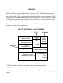
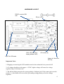
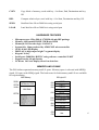
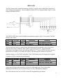
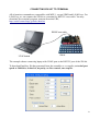
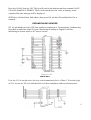
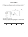
Z80 Microprocessor Kit
User's manual
Rev. 1.1, October 2015
Z80 MICROPROCESSOR KIT
USER'S MANUAL
CONTENTS
OVERVIEW...........................................................................................3
FUNCTIONAL BLOCK DIAGARM........................................................3
HARDWARE LAYOUT...........................................................................4
KEYBOARD LAYOUT............................................................................5
HARDWARE FEATURES......................................................................6
MEMORY AND I/O MAPS......................................................................6
GPIO1 LED.............................................................................................7
CONNECTING Z80 KIT TO TERMINAL................................................8
EXPANSION BUS HEADER..................................................................9
10ms TICK GENERATOR....................................................................10
RS232C PORT......................................................................................11
DATA FRAME for UART COMMUNICATION......................................11
CONNECTING LCD MODULE.............................................................12
LOGIC PROBE POWER SUPPLY........................................................12
HARDWARE SCHEMATIC, BOM, AND PCB LAYOUT.......................13
OVERVIEW
The Z80 microprocessor kit is a single board microcomputer designed for self learning.
Students will learn how to build the computer using the 1976, Z80 microprocessor with
memory and simple I/O chips. The kit can be assembled at home without the need of special
tools. The kit itself is the real microcomputer. Students will learn how to program the Z80
microprocessor in machine language with instruction hex code. The hex code can be entered
to memory and tested it directly. Results of CPU operations can be checked in the memory
or user registers display easily.
The kit manuals are 1) user's manual for hardware details, 2) programming lab book and 3)
construction guide for kit assemble steps.
Z80 KIT FUNCTIONAL BLOCK DIAGRAM
RS232C
32kB User RAM
Interfacing
bus
expansion
2400 Bit/s
UART
4kB Monitor ROM
PLD
decoder
Z80
Microprocessor
1.79MHz
Oscillator
AC adapter
+5VDC
power
supply
10ms tick
generator
16x2 Text LCD module 6-digit 7-segment display
Keyboard, hex key,
functions key and CPU
control key
8-bit debugging LED
Logic
speake
Probe
+5V supply
r
Notes
1. UART is software control for low speed asynchronous communication.
2. LCD module is optional, the kit provides a 16-pin header.
3. 10ms Tick generator is for a maskable interrupt source. NMI is used by single stepping
circuit.
3
HARDWARE LAYOUT
RS232C connector, DB9
male
DC jack, +9VDC
GPIO1 LED, 8-bit binary
display (address is 40H)
LCD contrast adj.
20-pin Text LCD header.
Selector for 10ms tick or
INTR key
Important Notes
1. Plugging or removing the LCD module must be done when the kit is powered off!
2. AC adapter should provide approx. +9VDC, higher voltage will cause the voltage
regulator chip, U9 becomes hot.
3. The kit has diode protection for wrong polarity of adapter jack. If the center pin is not the
positive (+), the diode will reverse bias, preventing wrong polarity to feed to voltage
regulator.
4
KEYBOARD LAYOUT
HEX keys
Hexadecimal number 0 to F with associated user registers and flag bits when
press REG
CPU control keys
RESET
MON
INTR
USER
Reset the CPU, Z80 will begin fetch the code from location 0000
Force CPU to jump back to monitor program
Make INT pin to logic low, used for experimenting with interrupt process
User key for lab test, active low
Monitor function keys
INS
Insert byte to memory, current byte will be shifting down.
DEL
Delete current byte, the next byte will be shifting up.
STEP
Execute user code only single instruction and return to save CPU registers
GO
Jump from monitor program to user code
SBR
Set break address
CBR
Clear break address
PC
Set current display address with user Program Counter
REG
Display user registers or flags with HEX key for a given register.
DATA
ADDR
Set entry mode of hex keys to Data field
Set entry mode of hex keys to Address field
5
COPY
Copy block of memory, used with key + for Start, End, Destination and key
GO
REL
Compute relative byte, used with key + for Start, Destination and key GO
SEND
Send Intel hex file at 2400 bit/s using serial port
LOAD
Load Intel hex file at 2400 bit/s using serial port
HARDWARE FEATURES
•
•
•
•
•
•
•
•
•
•
Microprocessor: Zilog Z80 @1.79MHz, 40-pin DIP package
Memory: 4kB monitor ROM, 32KB user RAM
Memory& I/O Decoder logic: GAL16V8
System tick: 10ms produced by AT89C2051 microcontroller
GPIO: 8-bit LED display
DISPLAY: 6-digit super bright 7-segment display
Keypad: 36-key
Serial port: 2400 Bit/s RS232C using software controlled UART
Expansion slot: 40-pin header
LCD bus: 16x2 text display direct bus interface
MEMORY AND I/O MAP
The Z80 kit has separated memory and I/O space. Memory space is selected with MREQ
signal, I/O space with IORQ signal. The bank areas for both memory and I/O are available
for experimenting.
256 bytes I/O
64kB Memory
0000H
0FFFH
1000H
4kB Monitor ROM
32kB RAM
8FFFH
FFFFH
00H
01H
02H
PORT0
PORT1
40H
GPIO1
PORT2
80H
81H
LCD command WR
LCD data WR
82H
83H
LCD command RD
C0HC3H
LCD data RD
User
6
GPIO1 LED
The Z80 kit provides a useful 8-bit binary display. It can be used to debug the program or
code running demonstration. The I/O address is 40H. U16 is 8-bit data latch. Logic 1 at the
output will make LED lit.
The GPIO1 LED can be used to display accumulator register easily. Let us take a look the
sample code below.
Address
Hex code
1800
3E 01
1802
D3 40
Label
MAIN
Instruction
comment
LD A,1
Load register A with 1
OUT (40H),A
Write A to GPIO1@ 40H
The test code has only two instructions. Each instruction has machine code of two bytes.
Enter the hex code to memory from 1800 to 1803. Then press PC, and execute the
instruction with single step by pressing key STEP. The 2nd pressed STEP key that executes
instruction out (40H),A will make the GPIO1 LED showing the content of register A.
Another sample is with JUMP instruction. The JUMP instruction will change the Program
Counter to 1800, to repeat program running.
Address
Hex code
1800
3C
1801
D3 40
1803
C3 00 18
Label
MAIN
Instruction
comment
INC A
Increment register A
OUT (40H),A
Write A to GPIO1@ 40H
JP MAIN
Jump back to main
Again enter the hex code to memory and test it with single step. Every time when
instruction out(40H),A was executed, did you see the LED display changed?
We will learn more the use of GPIO1 with Z80 Programming Lab Book.
7
CONNECTING Z80 KIT TO TERMINAL
All of monitor commands are compatible with MPF-1, except SEND and LOAD keys. For
LOAD key, we can connect the Z80 kit to a terminal by RS232C cross cable. You may
download free terminal program, teraterm from this URL,
http://ttssh2.sourceforge.jp/index.html.en
RS232C cross cable
VT100 Terminal
Z80 Kit
The example shows connecting laptop with COM1 port to the RS232C port of the Z80 kit.
To download Intel hex file that generated from the assembler or c compiler, set serial port
speed to 2400 bit/s, 8-data bit, no parity, no flow control, one stop bit.
8
Press key LOAD, then key GO. The kit will wait for the data stream from terminal. On PC,
Click file>Send File>LED.HEX. The kit will read the hex file, write to memory, when
completed the start message will be displayed.
SEND key will need Start, End address then press GO, the kit will send Intel hex file to
terminal.
EXPANSION BUS HEADER
JP1, 40-pin header provides CPU bus signals for expansion or I/O interfacing. Students may
learn how to make the simple I/O port, interfacing to Analog-to-Digital Converter,
interfacing to stepper motor or AC power circuits.
USER KEY
User key, S19 is one bit active low key switch connected to bit 6 of Port 0. To test the logic
of S19, we can use IN A,(0) and check bit 6 of the accumulator with test bit instruction.
9
10ms TICK GENERATOR
SW4 is a selector for interrupt source between key INTR or 10ms tick produced by
89C2051 microcontroller. Tick generator is software controlled using timer0 interrupt in the
89C2051 chip. The active low tick signal is sent to P3.7. For tick running indicator, P1.7
drives D15 LED.
Tick is a 10ms periodic signal for triggering the Z80 interrupt pin. When select SW4 to
Tick, the Z80 CPU can be triggered by a maskable interrupt. The 100Hz tick or 10ms tick
can be used to produce tasks that executed with multiple of tick. The Z80 kit lab look will
show how to use 10ms tick to make a digital timer.
10ms
10ms
10ms
10
RS232C PORT
The RS232C port is for serial communication. We can use a cross cable or null MODEM
cable to connect between the kit and terminal, or kit #1 to kit #2 for sending or receiving
hex file. The connector for both sides are DB9 female. We may build it or buying from
computer stores.
For new PC or laptop computer with USB port, we may
have the RS232C port by using
the USB to RS232 converter.
DATA FRAME for UART COMMUNICATION
Serial data that communicated between kit and terminal is asynchronous format. The Z80
kit has no UART chip, instead it uses software controlled to produce bit rate of 2400 bit/s.
The data frame is composed of start bit, 8-data bit and stop bit. For our kit, period = 1/2400
= 417 microseconds.
Since bit period is provided by machine cycle delay. Thus to send/receive serial data
correctly, all interrupts must be disabled.
11
CONNECTING LCD MODULE
JR1 is 20-pin header for connecting the LCD module. The example shows connecting the
16x2 lines text LCD module. R17 is a current limit resistor for back-light. R18 is trimmer
POT for contrast adjustment. The LCD module is interfaced to the Z80 bus directly. The
command and data registers are located in I/O space having address from 80H to 83H.
Be advised that plugging or removing the
LCD module must be done when the kit is
powered off.
Text LCD module accepts ASCII codes for
displaying the message on screen.
Without settings the LCD by software, no
characters will be displayed. The first line
will be black line by adjusting the R18 for contrast adjustment.
LOGIC PROBE POWER SUPPLY
The kit provides test points TP1(+5V) and TP2(GND) for using the logic probe. Students
may learn digital logic signals with logic probe easily. The important signals are RESET
(TP4) and CPU clock (TP3). Tick signal, however indicated by D15 LED blinking. Logic
probe can test it at P3.7 of the 89C2051 microcontroller directly. Red clip is for +5V and
Black clip for GND.
+ 5V at TP1
GND at TP1
12
HARDWARE SCHEMATIC, PARTS LIST AND PCB LAYOUT
C1
100pF
SW1
U4A
74LS14
R1
1k
R3
10k
C2
10uF
R8
10k
2
U4D
Y1
8
11
12
3
3.579MHz
74LS14
+5V
U4B
VCC
1k
R2
74LS14
D
CLK
VCC
14
1
2
3
6
7
Q
4
Q
U7
A
B
R0(1)
R0(2)
R9(1)
R9(2)
74LS90
C9
0.1uF
XTAL
U5B
9
12
9
8
11
74HC74
8
QA
QB
QC
QD
RESET
VCC
C10
0.1uF
TXD
XTAL
4
VCC
2
3
VCC
+
5
RESET
C5
10uF 16V
C11
0.1uF
D
20
1
5
4
2
3
6
7
8
9
VCC
Q
Q
TP4
1
U5A
5
CPU_CLK
1
TP3
3
27
CLK
M1
28
19
20
22
21
RFSH
24
6
WAIT
U1
M1
MREQ
IORQ
WR
RD
REFSH
HALT
WAIT
INT
NMI
RESET
BUSRQ
BUSAK
CLK
Z80
R6
10k
WAIT
1
+
select INTR source
3
2k
C6
1000uF 16V
R10
Tick 100Hz
R19
680
2
SW4
BUSRQ
6
25
23
26
16
17
VCC
INT
VCC
D3
POWER
1
C13
0.1uF
VIN
U9
LM7805/TO
LED
D15
R4
10k
CPU_CLK
BUSRQ
BUSAK
INT
HALT
MREQ
IORQ
WR
RD
R5
10k
18
*RESET
NMI
12
13
14
15
16
17
18
19
VOUT
11
74HC74
RESET
6
3
P3.7
P1.0/AIN0
P1.1/AIN1
P1.2
P1.3
P1.4
P1.5
P1.6
P1.7
Programmable timer
C12
0.1uF
AT89C2051
VCC
RST/VPP
XTAL1
XTAL2
P3.0/RXD
P3.1/TXD
P3.2/INTO
P3.3/INT1
P3.4/T0
P3.5/T1
U8
74LS14
U4C
CLK
4
PR
CL
1
5
1
M1
+
VCC
VCC
BREAK
+
9
C7
C8
0.1uF
VSS
29
D
C
RESET
C3
C18
100nF
0.1uF
3
A0
A1
A2
A3
A4
A5
A6
A7
A8
A9
A10
A11
A12
A13
A14
A15
D0
D1
D2
D3
D4
D5
D6
D7
30
31
32
33
34
35
36
37
38
39
40
1
2
3
4
5
14
15
12
8
7
9
10
13
D0
D1
D2
D3
D4
D5
D6
D7
MREQ
IORQ
A6
A7
A12
A13
A14
A15
A0
A1
INTR
SW2
A12
A13
A14
A15
1
2
U6
I
I
I
I
I
I
I
I
10
9
8
7
6
5
4
3
25
24
21
23
2
26
22
20
27
1
I/CLK
I/OE
U2 27C64/27C256
12
13
14
15
16
17
18
19
R9
1k
+5V
Date:
Size
B
Title
11
12
13
15
16
17
18
19
D0
D1
D2
D3
D4
D5
D6
D7
VCC
+
GPIO1
A0
A1
A2
A3
A4
A5
A6
A7
A8
A9
A10
A11
A12
A13
A14
20
22
27
10
9
8
7
6
5
4
3
25
24
21
23
2
26
1
D0
D1
D2
D3
D4
D5
D6
D7
U3
1
D0
D1
D2
D3
D4
D5
D6
D7
D0
D1
D2
D3
D4
D5
D6
D7
HM62256B
A0
A1
A2
A3
A4
A5
A6
A7
A8
A9
A10
A11
A12
A13
A14
WR
RD
CE
OE
WE
0x1000-0x8FFF
JP1
2
4
6
8
10
12
14
16
18
20
22
24
26
28
30
32
34
36
38
40
1
HEADER 20X2
1
3
5
7
9
11
13
15
17
19
21
23
25
27
29
31
33
35
37
39
1
Sheet
Expansion Bus
WR
RD
RAMCE
RD
WR
LCD_E
PORT0
PORT1
PORT2
A11
A12
A13
A14
A15
CPU_CLK
D4
D3
D5
D6
D2
D7
D0
C4
100uF D1
INT
NMI
HALT
MREQ
IORQ
VCC
VCC
Saturday, January 17, 2015
Document Number
<Doc>
Z80 MICROPROCESSOR KIT
HALT
ROMCE
RAMCE
A0
A1
O0
A2
O1
A3
O2
A4
O3
A5
O4
A6
O5
A7
O6
A8
O7
A9
A10
A11
A12
A13
OE
CE
PGM
VPP
0x0000-0x0FFF (4kB)
I/O/Q
I/O/Q
I/O/Q
I/O/Q
I/O/Q
I/O/Q
I/O/Q
I/O/Q
2
LED
D1
R7
680
GAL16V8B
VCC
2
DC input
BC557
Q1
1
11
2
3
4
5
6
7
8
9
RD
ROMCE
VCC
J1
A0
A1
A0
A1
A2
A3
A4
A5
A6
A7
A8
A9
A10
A11
1
TVS5V_SOD123
D2
1N4007
D4
VCC
2
DC2
3
1
10uF
SW3
MONITOR
TP1
+5V
1
TP2
1
4
2
B
A
GND
5
GND
2
PR
10
CL
13
11
12
13
15
16
17
18
19
3
D0
D1
D2
D3
D4
D5
D6
D7
RD
WR
BUSAK
WAIT
BUSRQ
*RESET
M1
RFSH
A0
A1
A2
A3
A4
A5
A6
A7
A8
A9
A10
of
Rev
2
D
C
B
A
D
C
B
A
WR
D0
D1
D2
D3
D4
D5
D6
D7
1
2
D0
D1
D2
D3
D4
D5
D6
D7
U13A
4001
9
8
RESET
WR
PORT1
PORT2
RD
PORT0
3
U13C
4001
5
5
D0
D1
D2
D3
D4
D5
D6
D7
D0
D1
D2
D3
D4
D5
D6
D7
D0
D1
D2
D3
D4
D5
D6
D7
10
U13B
+5V
5
6
4001
13
VCC
VCC
U4F
2
3
4
5
6
7
8
9
11
1
20
2
3
4
5
6
7
8
9
11
1
20
4
18
17
16
15
14
13
12
11
1
19
74LS14
U12
1Q
2Q
3Q
4Q
5Q
6Q
7Q
8Q
0x02
VCC
1D
2D
3D
4D
5D
6D
7D
8D
LE
OE
VCC
0x01
74HC573
U14
1Q
2Q
3Q
4Q
5Q
6Q
7Q
8Q
0x01
1D
2D
3D
4D
5D
6D
7D
8D
LE
OE
U15
A1
A2
A3
A4
A5
A6
A7
A8
19
18
17
16
15
14
13
12
19
18
17
16
15
14
13
12
20
2
3
4
5
6
7
8
9
TXD
74HC573
VCC
0x00
Y1
Y2
Y3
Y4
Y5
Y6
Y7
Y8
G1
G2
VCC
74HC541
12
E
G
F
A
B
C
DP
D
PA0
PA1
PA2
PA3
PA4
PA5
PA6
11
4
S19
PC7 SPEAKER
VCC
VCC
RXD
4
PC0
PC1
PC2
PC3
PC4
PC5
PC6
A
B
C
D
E
F
G
DP
U4E
74LS14
10
14
16
13
3
5
11
15
7
U10
A
B
C
D
E
F
G
DP
LTC-4727JR
PC5
PC4
PC3
PC2
PC1
PC0
S1
S7
S13
S20
S26
S30
BREAK
3
S2
S8
S14
S21
S27
S31
3
S3
S9
S15
S22
S28
S32
2
14
16
13
3
5
11
15
7
U11
A
B
C
D
E
F
G
DP
S6
A
B
C
D
E
F
G
DP
S5
S12
4
S4
S11
S18
L1L2L3
S10
S17
S25
LTC-4727JR
S16
S24
S33
S29
S23
2
R14
330
R13
1
7-segment test
2
1
J2
4
3
VCC
VCC
CON3
1
2
3
L1L2L3
1
of
SPEAKER
+5V
LS1
C
R12
2
C
R16
10
R15
Q2
BC557
10k RESISTOR SIP 9
PC0
2
PC1
3
PC2
4
PC3
5
PC4
6
PC5
7
8
9
4.7k
D5
1
Sheet
10k RESISTOR SIP 9
2
3
4
5
6
7
8
9
TONE
PA0
PA1
PA2
PA3
PA4
PA5
PA6
Saturday, January 17, 2015
Document Number
<Doc>
Z80 TRAINER KIT
VCC
SPEAKER
Title
Size
B
Date:
1
3
DIGIT4
8
DIGIT3
6
DIGIT2
2
DIGIT1
1
DIGIT4
8
DIGIT3
6
DIGIT2
2
DIGIT1
1
Rev
2
D
C
B
A
WR
D0
D1
D2
D3
D4
D5
D6
D7
12
13
5
U13D
4001
R17
D7
D6
D5
D4
D3
D2
D1
D0
11
VCC
10
R/W
RS
+5V
+5V
RD
2
3
4
5
6
7
8
9
A1
20
11
1
WR
VCC
LCD_E
+5V
RD
WR
U16
1D
2D
3D
4D
5D
6D
7D
8D
LE
OE
VCC
1Q
2Q
3Q
4Q
5Q
6Q
7Q
8Q
4
0x40
74HC573
A0
19
18
17
16
15
14
13
12
VCC
VCC
D6
D7
LED
D8
D9
D10
1N5236A
D14
3
LED
D11
8-bit Binary display LED x8
D12
D13
VB1
5
9
4
8
3
7
2
6
1
+5V
2
14
7
13
8
6
2
10uF 10V
C14
C16
10uF
SUB-D 9, Male (cross cable)
2
U17
V+
V-
T1OUT
T2OUT
R1IN
R2IN
MAX232A
Title
Size
B
+5V
C+
C1C2+
C2-
T1IN
T2IN
R1OUT
R2OUT
10uF C15
1
3
4
5
11
10
12
9
Z80 TRAINER KIT
Document Number
<Doc>
10uF
1
TXD
1
VCC
Sheet
RXD
VCC
C17
Saturday, January 17, 2015
+
Date:
+
+5V
D0
D1
D2
D3
D4
D5
D6
D7
A1
A0
3
3
+
D0
D1
D2
D3
D4
D5
D6
D7
GPIO1
RESET
16
15
14
13
12
11
10
9
8
7
6
5
4
3
2
1
16x2 text LCD interface
JR1
16
15
14
13
12
11
10
9
8
7
6
5
4
3
2
1
CONN RECT 16
1
R18
10K
4
+
D
C
B
A
5
2
3
of
3
Rev
1
D
C
B
A
PARTS LIST
Capacitors
Semiconductors
U1
Z80 40-pin DIP microprocessor
U2
27C64 or 27C256 EPROM
U3
HM62256B 32kB SRAM
U4
74LS14 inverter
U5
74HC74 Dual D-type flip-flop
U6
GAL16V8B programmable logic device
U7
74LS90 decade counter
U8
AT89C2051 20-pin microcontroller
U9
LM7805/TO voltage regulator
U11,U10 LTC-4727JR 4-digit 7-segment LED
U12,U14,U16 74HC573 8-bit latch
U13 CD4001 quad NOR gate
U15 74HC541 tri-state buffer
U17 MAX232A rs232 converter
D1,D6,D7,D8,D9,D10,D11, 3mm LED
D12,D13,D15
D2
TVS5V_SOD123 transient voltage
suppressor
D4
1N4007 rectifying diode
D14 1N5226A +3.3V zener 500mW
Q2,Q1 BC557 PNP transistor
D3
POWER 3mm LED
D5
TONE 3mm LED
Resistors (all resistors are 1/8W +/-5%)
R1,R2,R9
1k
R3,R4,R5,R6,R8,R18 10K
R7,R19
680 Ohms
R10
2k
R16,R12
10k RESISTOR SIP 9
R13
4.7k
R14
330 Ohms
R17,R15
10 Ohms
C1
100pF ceramic
C2,C3,C15,C16,C17 10uF electrolytic
C4
100uF electrolytic
C5
10uF 16V electrolytic
C6
1000uF 16V electrolytic
C7,C8,C9,C10,C11 0.1uF multi layer
C12,C13
0.1uF multilayer
C14 10uF 10V electrolytic
C18 0.1uF multilayer
Additional parts
JP1
JR1
J1
J2
LS1
HEADER 20X2
CONN RECT 16 pins
DC input JACK
HEADER 3 pins
8 Ohms SPEAKER
SW1
SW2
SW3
SW4
RESET 12mm tact switch
INTR 12mm tact switch
MONITOR 12mm tact switch
slide switch-SPDT
S1,S2,S3,S4,S5,S6,S7,S8, 12mm TACT switch
S9,S10,S11,S12,S13,S14,
S15,S16,S17,S18,S19,S20,
S21,S22,S23,S24,S25,S26,
S27,S28,S29,S30,S31,S32,
S33
VB1 DB 9, Male connector
Y1
XTAL 3.579MHz
PCB double side plate through hole
LED cover Clear RED color acrylic plastic
Keyboard sticker printable SVG file
SILK SCREEN TOP LAYER
TOP LAYER
BOTTOM LAYER
NOTE