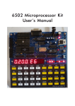
1
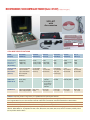
MICROPROCESSOR / MICROCONTROLLER TRAINER (Model : XPO-KIT) [a family of training systems]
XPO-KIT
with
Accessories
XPO-KIT IG
XPO-KIT SW
CPU WISE SPECIFICATIONS
MODEL
CPU (bits)
XPO-85/Z80
8085/Z80 (8)
XPO-88/86
8088/86 (8/16)
XPO-51/31
8051/31(8)
XPO-97/196
8096/196(16)
XPO 68K
68000(16/32)
XPO 11
68HC11 (8)
MEMORY CAPA.
Monitor EPROM
Battery Back Up
Scratch Pad
(Expandability)
36KB(64 KB)
16KB(64 KB)
4KB( 8 KB)
128 KB
64 KB (128 KB)
64 KB ( 64 KB)
36 KB
16 KB (64KB)
2 KB ( 8KB)
24KB
16KB
8KB
128KB
64KB (128 KB)
64KB
24KB
20KB
8KB
ADVANCED S/W
Assembler
Disassembler
(Optional)
1 Pass line assembler
2 pass Assembler
2 pass Disassembler
Basic Interpreter
Hex Dump
Line assembler
Disassembler,
Hex Dump.
1 Pass
line assembler
Disassembler
Disassembler
and assembler
facility with
S/W on floppy.
1 Pass
line assembler
Disassembler
1 Pass
line assembler
Disassembler
ADDITIONAL
SERIAL AND
PARALLEL I/O
SID/SOD
Based (8085)
NA (Z80)
NA
l
Using built-in
TxD/RxD
Using built-in
TxD/RxD (6850)
Using built-in
TxD/RxD
INTERRUPTS
8 Nos.Using 8259(8085) 8Nos. Using
4 Nos. Using CTC(Z80) 8259A
Built in CPU
8 no. of Ints.
Built in CPU
7 no. of Ints.
Built in CPU
7 no. of Ints.
l
Using built-in
TxD/RxD
Unused pins of
P1 port offered
through 10 pin
reliamate.
Built in CPU
2no. of ints.
8088/8086- Sockets provided for NDP 8087 And I/O controller 8089 .
8051/8031- Optionally I2C Bus Using 24C02 (512 x 8)EEPROM and Optionally RTC DS1307.
8097/196 - 8 nos. of Quasi Bi-directional port lines (CPU Ports),High Speed I/O Lines : 8 High Speed TTL, 4 dedicated I/O Lines & 4
Nos. Programmable I/O Lines. A/D converter 8 Channel 10 Bit A to D Converter with onboard Potentiometer for demonstration.
Timers - 2 Nos. of 16 Bit Timers from 8097/196,and 3 Nos from 8253.Watch Dog Timer from 8097.
PWM O/P - PWM O/P (Provides Pulse Train with variable duty cycle).Inbuilt 256 bytes RAM.
8085 and 8086 - Optional study card set (PERIWARES) compatible to trainers with LED's for indicating signals like READ, WRITE, CHIP
SELECT, DATA LINES, etc, for peripheral IC's 8251, 8253, 8255, 8257, 8155, 8279, 8259, 6116, with bus converter (cum RE) Card &
two 50 pin FRC cables to attach.
CPU CARD:
8085
Z80
8086
8051
68K
68HC11
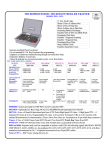
TECHNICAL SPECIFICATIONS
User Manual
1) Student Workbook 2) Instructor Guide and Technical Reference
3) Optionally Lab Exercise Book common for 85, 86 & 51.
Speed
20 MHz crystal operated multi-output clock source to operate various resources on
Mother Board like CPU, Baud rate, T/C etc.
Parallel I/O
48 I/O lines using two 8255 through 2 Nos. of 26 pin FRC header, printer I/F.
Serial I/O
RS-232c serial interface using 8251 and RS232 driver IC through 9 Pin male D connector.
Timer counter
3 Nos. T/C using 8253 pins brought out on 6 pin reliamate.
Display(Choose one option)
16 X 2 LCD (Backlit)
Key Board (Optional)
Single chip micro- controller 89C2051 to support 101Keys PC AT / PS2 Keyboard and LCD
System Bus
50 Pin FRC buffered Bus to connect periware cards as well as to facilitate ROM Emulation of 8 bit/16
bit system memory using external ROM emulation card cum converter card.
Battery Backup
Rechargeable NiCd battery (3.6/60maH) provided to supply power to battery backup
memory and Optional RTC 58167.
Onboard Features
l
l
l
l
l
l
16 X 2 Jumbo LCD (Backlit)
20 X 4 LCD (Backlit)
External Loud Speaker (8ohm/0.5W) interface for experiments on frequency synthesis.
Reset and Single Step/Interrupt push button.
EP socket for experiments with Cassette recorder interface.
Programmable Wait state generator l Real Time Clock IC 58167 (Optional)
11 Nos. fault links to teach troubleshooting skills by introducing faults in the circuit.
PALs-All glue logic like Memory I/O decoders are implemented using 4(5) nos. of
EEPROM PALs 16V8
Power Supply (SMPS)
(Optional)
Select one of 2 options I) 5V /2.5 Amp SMPS with RCA plug. (Only for Kit)
II) 5V /2.5 Amp SMPS with RCA plug +12 V/ 850 mA , -12V/250 mA with 4 pin reliamate SMPS.
Mechanical
Aesthetically designed Injection molded plastic enclosure of size 215(L)X165(W) X 75(H) mm.
Cables & CD : 9 Pin Female to 9 Pin Female RS-232c Cable, 26 Pin FRC IO Cable, Centronics Interface cable (26 pin FRC to 36 pin
Centronics female), USB to RS232 Cable (optional), Sample program on CD .
SALIENT FEATURES
Fault Links:
l
Shorts 2 Pins of Address Bus.
l
Shorts 2 Pins of Data Bus.
l
Shorts Address pin to Data Bus.
l
Permanent Wait State.
l
Increasing Battery Discharge.
l
Stops 20MHz Clock.
l
Disables 7 Segment Scanning.
l
l
Disables 7 Segment Data.
l
l
Disables RD/ & WR/ into BBK RAM
u
u
Ergonomical injection molded Plastic enclosure.
Use of standard PC 101/PS2 Keyboard for programming.
u
Emphasis on Hardware troubleshooting through on board short
links.
Permanent Reset State.
u
Exhaustive Didactic Courseware.
Disables Baud Rate Clock.
u
Critical & delicate ICs are protected under acrylic cover from
below.
u
All in one Logical IO Monitor design Supports both serial IO
®
& Keyboard display console IO.
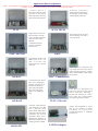
Application Board (Optional):
Note : 1] Compatible with XPO KIT as well as XPO EST. 2] All ECUs may not be capable of driving following Application boards
in totality on account of their memory, IO, resource limitation. I/O port based :
Traffic light of 2
intersections cum logic study
card with 24 tags and 24
LED's.Optionally following
Opto-coupler, Relay, Buzzer.
TLLC
S c a n n i n g Te c h n i q u e s
illustrating 8X8 LED Matrix,
4X4 Keypad 7 segment 8 digit
red LED display study card.
SCAN TECH
Stepper motor and 12V DC
Motor Interface card with
motors mounted to illustrate
speed, direction control.
Optional:
1) RPM measurement.
2) LM35 temperature
Sensor 0-12V)
STDC MOTOR
Opto-isolated 24 Vdc 12 Input
and 10 Output IO card with 2
relay output card.
IOOC
Temperature Controller with
MINI OVEN with 8 bit
ADC- 8 bit DAC cum
Instrumentation Opamp
study card.
Traffic light of 2 intersections cum
logic study card with 24 tags and 24
LED's. Optionally following - ThumbWheel Switch Module, Opto-coupler,
Relay, Buzzer.
AD-DA-I
TLLC+Thumbwheel
8 bit 8 channel ADC & 8 bit
DAC (0-5V), Digital gain
amplifier with built in L/S
interface Electret microphone with preamplifier,
light sensor, analog bar
graph, voice sampling &
relay.
AD-DA-II
Traffic light of 2 intersections cum
logic study card with 24 tags and 24
LED's. Optionally following Elevator SAP consisting of 3 floors,
Floor request keys, child protection
lock, Opto-coupler, Relay, Buzzer.
TLLC+ Elevator
12 bit ADC either dual slope
7109 OR SAR 574 or SPI
3301, 12 Bit DAC: Either
parallel R-2R CMOS DAC
or SPI 4921, onboard voltage
simulation pot, LM 35
temperature sensor (0-5V),
buffered S/H amplifier, 16
differential channel MUX &
variable gain instru. OPMP.
AD-DA-III
Adaptor PCB mountable on 26-pin
FRC IO box connector to facilate
attachment of external LCD
{Graphic/text}module or additional
8255/8155 IC.
LCD IO Adaptor
Bus based Application Board (optional)
Note : VCRO CARD applicable for XPO-KIT & not EST.
VCRO Card:
VGA monitor(64X32) /
Oscilloscope (18 X 8)
interface card to use them as
console out device for the kit
in place of LCD/7seg. Use
20MHz CRO with Z Input
(1.25MHz Band width) & Ext.
Triggering facility.
Ethernet Application Module (RTL 8019)
• Ethernet card applicable for XPO-EST
& not for XPO-KIT.
• Operates on 22 Pin Bus [data (8),
address (18), control]
Periwares Study Card Set
Optional for Kit 85/86/51 Kit.
It consists of buffers, switches
& debounce circuits for software
single stepping of every access,
1 no 6116 (RAM) with tags for
applying Interrupts, Vcc tags,
Leds to display status.
ROM Emulation cum converter Card
2 No. 28 pin DIP connectors for 8 bit/16 bit
ROM connection of target uc, two 50 pin
FRC cables to attach for periware.
Memory IO
It consists of buffers, switches &
debounce circuits for software
single stepping of every access.
It is provided with one 8 bit I/O
port. It displays the data
transferred (DMA Read) from
memory to the port on the LEDS.
8257
It consists of buffers, switches,
debounce ckts for software
Single Stepping, one 8255 with
tags for all I/O ports, VCC &
GND tags, LEDs to display
status.
8255
It consists of buffers, switches
and debounce circuit for
software single stepping of every
access to the 8279 card and
LEDs to display status. Switch
S1 is used to enable Single
stepping or to keep CPU in free
running mode.
8279
It consists of buffers, switches,
debounce circuits for software
Single Stepping, one 8253 with
tags for all the counters, VCC &
GND tags, LEDs to display
status.
8253
It consists of buffers, switches
& debounce circuits for software
single stepping of every access,
2 nos of 8259 with tags for
applying Interrupts, Vcc tags,
Leds to display status.
8259
It consists of buffers, switches,
debounce circuits for software
Single Stepping, one 8251 with
tags for all the required input
output pins, Vcc & Ground tags,
LEDs to display status
8251