1
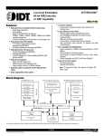
Ò FOURTH GENERATION 64-BIT RISC MICROPROCESSOR IDT79R4600 Integrated Device Technology, Inc. FEATURES: • True 64-bit microprocessor - 64-bit integer operations - 64-bit floating-point operations - 64-bit registers - 64-bit virtual address space • High-performance microprocessor - 150 peak MIPS at 150MHz - 50peak MFLOP/s at 150MHz - 96 SPECint92 at 150Mz - Two-way set associative caches • High level of integration - 64-bit integer CPU - 64-bit floating-point unit - 16KB instruction cache; 16KB data cache - Flexible MMU with large TLB • Low-power operation - 3.3V or 5V power supply options - 20mW/MHZ typical internal power dissipation (2.0W @ 100MHz, 3.3V) • • • • • • - Standby mode reduces internal power to 90mA @ 5V and 60mA @ 3.3V (450mW @ 5V and 400mW @ 3.3V). Standard operating system support includes: - Microsoft Windows NT - UNISOFT Unix System V.4 Fully software compatible with R4000 RISC Processor Family Available in R4000PC/R4000PC pin-compatible 179-pin PGA or 208-pin MQUAD 50MHz, 67MHz, 75MHz input frequencies with mode bit dependent output clock frequencies - On-chip clock doubler for 150MHz pipeline 64GB physical address space Processor family for a wide variety of applications - Desktop workstations and PCs - Deskside or departmental servers - High-performance embedded applications (e.g. color printers, multi-media and internetworking.) - Notebooks BLOCK DIAGRAM: Data Tag A Data Set A Instruction Set A DTLB Physical Store Buffer Data Tag B SysAD Instruction Select Write Buffer Address Buffer Read Buffer Instruction Tag A Instruction Register ITLB Physical Data Set B Instruction Set B Instruction Tag B DBus IBus Control Tag Floating-point Add/Sub/Cvt/Div/Sqrt Integer Divide Joint TLB Floating-point Control Unpacker/Packer AuxTag Floating-point/Integer Multiply Coprocessor 0 DVA Integer Control Floating-point Register File Load Aligner Integer Register File Integer/Address Adder Data TLB Virtual Shifter/Store Aligner Logic Unit PC Incrementer System/Memory Control Branch Adder IVA Phase Lock Loop, Clocks Instruction TLB Virtual Program Counter 3038 drw 01 The IDT logo is a registered trademark and Orion, R4600, R4400, R3081, R3052, R3051, R3041, RISController, and RISCore are trademarks of Intergrated Device Technology, Inc. All others are trademarks of their respective companies. COMMERCIAL TEMPERATURE RANGE 1994 Integrated Device Technology, Inc. March 1994 5.7 DSC 9075/1 1 IDT79R4600 COMMERCIAL TEMPERATURE RANGE DESCRIPTION: operating systems and applications. The 64-bit computing and addressing capability of the R4600 enables a wide variety of capabilities previously limited by a smaller address space. For example, the large address space allows operating systems with extensive file mapping; direct access to large files can occur without explicit I/O calls. Applications such as large CAD databases, multi-media, and high-quality image storage and retrieval all directly benefit from the enlarged address space. This data sheet provides an overview of the features and architecture of the R4600 CPU. A more detailed description of the processor is available in the “IDT79R4600 Processor Hardware User’s Manual”, available from IDT. Further information on development support, applications notes, and complementary products are also available from your local IDT sales representative. The IDT79R4600 supports a wide variety of processorbased applications, from 32-bit Windows NT desktop or notebook systems through high-performance, 64-bit OLTP systems. Compatible with the IDT79R4000PC family for both hardware and software, the R4600 will serve in many of the same applications, but, in addition supports lowpower operation for applications such as “green” desktops and notebook computers. It does not provide integrated secondary cache and multiprocessor support as found in the R4000SC and R4000MC, but an external secondary cache can lastly be designed around it. The large on-chip two-way set associative caches make this unnecessary in most embedded control applications. The R4600 brings R4000SC performance levels to the R4000PC package, while at the same time providing lower cost and lower power. It does this by providing larger onchip caches that are two-way set associative, fewer pipeline stalls, and early restart for data cache misses. The result is 102 SPECint92 and >90SPECfp92 (exact figures are system-dependent). The R4600 provides complete upward application-software compatibility with the IDT79R3000 family of microprocessors, including the IDT RISController 79R3051 / R3052 /R3041 /R3071 /R3081 as well as the IDT79R4000 family of microprocessors. Microsoft Windows NT and UNISOFT Unix V.4 operating systems insure the availability of thousands of applications programs, geared to provide a complete solution to a large number of processing needs. An array of development tools facilitates the rapid development of R4600-based systems, enabling a wide variety of customers to take advantage of the MIPS Open Architecture philosophy. Together with the R4000 family, the R4600 provides a compatible, timely, and necessary evolution path from 32bit to true, 64-bit computing. The original design objectives of the R4000 clearly mandated this evolution path; the result is a true 64-bit processor fully compatible with 32-bit HARDWARE OVERVIEW The R4600 family brings a high-level of integration designed for high-performance computing. The key elements of the R4600 are briefly described below. A more detailed description of each of these subsystems is available in the User’s Manual. Pipeline The R4600 uses a 5-stage pipeline similar to the IDT79R3000. The simplicity of this pipeline allows the R4600 to be lower cost and lower power than super-scalar or super-pipelined processors. Unlike the R3000, the R4600 does virtual-to-physical translation in parallel with cache access. This allows the R4600 to operate at twice the frequency of the R3000 and to support a larger TLB for address translation. Compared to the 8-stage R4000 pipeline, the R4600 is more efficient (requires fewer stalls). Figure 2 shows the R4600 pipeline. Figure 1. CPU Registers General Purpose Registers 63 0 Multiply/Divide Registers 0 63 r1 0 HIGH r2 63 • 0 LOW • • Program Counter • 63 r29 0 PC r30 r31 5.7 2 IDT79R4600 COMMERCIAL TEMPERATURE RANGE Figure 2. R4600 Pipeline I0 1I I1 2I 1R 2R 1A 2A 1D 2D 1W 2W 1I 2I 1R 2R 1A 2A 1D 2D 1W 2W 1I 2I 1R 2R 1A 2A 1D 2D 1W ••• 1I 2I 1R 2R 1A 2A 1D ••• 1I 2I 1R 2R 1A ••• I2 I3 I4 one cycle 1I-1R Instruction cache access 2I 2A-2D 1D 1D-2D 2R 2R 2R 2R 1A 1A-2A 1A 2A 1A 2W Instruction virtual to physical address translation in ITLB Data cache access and load align Data virtual to physical address translation in DTLB Virtual to physical address translation in JTLB Register file read Bypass calculation Instruction decode Branch address calculation Issue or slip decision Integer add, logical, shift Data virtual address calculation Store align Branch decision Register file write Integer Execution Engine The R4600 implements the MIPS Instruction Set architecture, and thus is fully upward compatible with applications running on the earlier generation parts. The R4600 includes the same additions to the instruction set as found in the R4000 family of microprocessors, targeted at improving performance and capability while maintaining binary compatibility with earlier processors. The extensions result in better code density, greater multi-processing support, improved performance for commonly used code sequences in operating system kernels, and faster execution of floating-point intensive applications. All resource dependencies are made transparent to the programmer, insuring transportability among implementations of the MIPS instruction set architecture. In addition to the instruction extensions detailed above, new instructions have been defined to take advantage of the 64-bit architecture of the processor. When operating as a 32-bit processor, the R4600 will take an exception on these new instructions. The MIPS integer unit implements a load/store architecture with single cycle ALU operations (logical, shift, add, sub) and autonomous multiply/divide unit. The register resources include: 32 general-purpose orthogonal integer registers, the HIGH/LOW result registers for the integer multiply/divide unit, and the program counter. In addition, the on-chip floating-point co-processor adds 32 floating- point registers, and a floating-point control/status register. Register File The R4600 has thirty-two general-purpose registers. These registers are used for scalar integer operations and address calculation. The register file consists of two read ports and one write port, and is fully bypassed to minimize operation latency in the pipeline. ALU The R4600 ALU consists of the integer adder and logic unit. The adder performs address calculations in addition to arithmetic operations, and the logic unit performs all logical and shift operations. Each of these units is highly optimized and can perform an operation in a single pipeline cycle. Integer Multiply/Divide The R4600 uses the floating-point unit to perform integer multiply and divide. The results of the operation are placed in the HIGH and LOW registers. The values can then be transferred to the general purpose register file using the MFHI/MFLO instructions. Table 1 below shows the number of processor internal cycles required between an integer multiply or divide and a subsequent MFHI or MFLO operation, in order that no interlock or stall occurs. 5.7 3 IDT79R4600 COMMERCIAL TEMPERATURE RANGE Table 2: Floating-Point Cycles Table 1: Integer multiply/divide cycles 32-bit 64-bit MULT 10 12 DIV 42 74 Floating-Point Co-Processor The R4600 incorporates an entire floating-point co-processor on chip, including a floating-point register file and execution units. The floating-point co-processor forms a “seamless” interface with the integer unit, decoding and executing instructions in parallel with the integer unit. Double Precision ADD 4 4 SUB 4 4 MUL 8 8 DIV 32 61 SQRT 31 60 CMP 3 3 FIX 4 4 FLOAT 6 6 ABS 1 1 MOV 1 1 NEG 1 1 LWC1, LDC1 2 2 SWC1, SDC1 1 1 System Control Co-processor (CP0) The system control co-processor in the MIPS architecture is responsible for the virtual memory sub-system, the exception control system, and the diagnostics capability of the processor. In the MIPS architecture, the system control co-processor (and thus the kernel software) is implementation dependent. The R4600 CP0 is essentially identical to that of the R4000PC, except that the WatchLo and WatchHi registers are no longer present and the Index CACHE ops use an extra address bit to select one of the two sets (the R4000 caches are direct mapped, instead of two-way set associative). The Memory management unit controls the virtual memory system page mapping. It consists of an instruction address translation buffer (the ITLB), a data address translation buffer (the DTLB), a Joint TLB (the JTLB), and coprocessor registers used for the virtual memory mapping sub-system. Table 2: Floating-Point Cycles Single Precision Double Precision Floating-Point General Register File The floating-point register file is made up of thirty-two 64bit registers. With the LDC1 and SDC1 instructions the floating-point unit can take advantage of the 64-bit wide data cache and issue a co-processor load or store doubleword instruction in every cycle. The floating-point control register space contains two registers; one for determining configuration and revision information for the coprocessor and one for control and status information. These are primarily involved with diagnostic software, exception handling, state saving and restoring, and control of rounding modes. Floating-Point Units The R4600 floating-point execution units supports single and double precision arithmetic, as specified in the IEEE Standard 754. The execution unit is broken into a separate multiply unit and a combined add/convert/divide/square root unit. Overlap of multiplies and add/subtract is supported. The multiplier is partially pipelined, allowing a new multiply to begin every 6 cycles. As in the IDT79R3010A and IDT79R4000, the R4600 maintains fully precise floating-point exceptions while allowing both overlapped and pipelined operations. Precise exceptions are extremely important in mission-critical environments, such as ADA, and highly desirable for debugging in any environment. The floating-point unit’s operation set includes floatingpoint add, subtract, multiply, divide, square root, conversion between fixed-point and floating-point format, conversion among floating-point formats, and floating-point compare. These operations comply with the IEEE Standard 754. Table 2 below gives the latencies of some of the floatingpoint instructions in internal processor cycles. Operation Single Precision Operation System Control Co-Processor Registers The R4600 incorporates all system control co-processor (CP0) registers on-chip. These registers provide the path through which the virtual memory system’s page mapping is examined and changed, exceptions are handled, and operating modes are controlled (kernel vs. user mode, interrupts enabled or disabled, cache features). In addition, the R4600 includes registers to implement a real-time cycle counting facility, to aid in cache diagnostic testing, and to assist in data error detection. Figure 5 shows the CP0 registers. 5.7 4 IDT79R4600 COMMERCIAL TEMPERATURE RANGE Virtual to Physical Address Mapping The R4600 provides three modes of virtual addressing: • user mode • supervisor mode • kernel mode This mechanism is available to system software to provide a secure environment for user processes. Bits in a status register determine which virtual addressing mode is used. In the user mode, the R4600 provides a single, uniform virtual address space of 256GB (2GB for 32-bit mode). When operating in the kernel mode, four distinct virtual address spaces, totalling 1024GB (4GB in 32-bit mode), are simultaneously available and are differentiated by the high-order bits of the virtual address. The R4600 processors also support a supervisor mode in which the virtual address space is 256.5GB (2.5GB in 32bit mode), divided into three regions based on the highorder bits of the virtual address. Figure 4 shows the address space layout for 32-bit operation. When the R4600 is configured as a 64-bit microprocessor, the virtual address space layout is an upward compatible extension of the 32-bit virtual address space layout. amount of mapped space, and the replacement characteristics of various memory regions. First, the page size can be configured, on a per-entry basis, to map a page size of 4KB to 16MB (in multiples of 4). A CP0 register is loaded with the page size of a mapping, and that size is entered into the TLB when a new entry is written. Thus, operating systems can provide special purpose maps; for example, a typical frame buffer can be memory mapped using only one TLB entry. The second mechanism controls the replacement algorithm when a TLB miss occurs. The R4600 provides a random replacement algorithm to select a TLB entry to be written with a new mapping; however, the processor provides a mechanism whereby a system specific number of mappings can be locked into the TLB, and thus avoid being randomly replaced. This facilitates the design of real-time systems, by allowing deterministic access to critical software. The joint TLB also contains information to control the cache coherency protocol for each page. Specifically, each page has attribute bits to determine whether the coherency algorithm is: uncached, non-coherent write-back, noncoherent write-through write-allocate, non-coherent writethrough no write-allocate. Non-coherent write-back is typically used for both code and data on the R4600; the writethrough modes support more efficient frame buffer accesses than the R4000 family, cache coherency is not supported, however. Joint TLB For fast virtual-to-physical address decoding, the R4600 uses a large, fully associative TLB which maps 96 Virtual pages to their corresponding physical addresses. The TLB is organized as 48 pairs of even-odd entries, and maps a virtual address and address space identifier into the large, 64GB physical address space. Two mechanisms are provided to assist in controlling the Instruction TLB The R4600 also incorporates a 2-entry instruction TLB. Each entry maps a 4KB page. The instruction TLB improves performance by allowing instruction address Figure 3. The R4600 CP0 Registers PageMask 5* EntryLo0 2* EntryHi 10* EntryLo1 3* 47 Index 0* TLB Random 1* (entries protected from TLBWR) Wired 6* Count 9* Compare 11* Status 12* Cause 13* EPC 14* ErrorEPC 30* Context 4* XContext 20* BadVAddr 8* LLAddr 17* PRId 15* Config 16* TagHi 29* TagLo 28* ECC 26* CacheErr 27* 0 * Register number 5.7 5 IDT79R4600 COMMERCIAL TEMPERATURE RANGE translation to occur in parallel with data address translation. When a miss occurs on an instruction address translation, the least-recently used ITLB entry is filled from the JTLB. The operation of the ITLB is invisible to the user. Cache Memory In order to keep the R4600’s high-performance pipeline full and operating efficiently, the R4600 incorporates onchip instruction and data caches that can be accessed in a single processor cycle. Each cache has its own 64-bit data path and can be accessed in parallel. The cache subsystem provides the integer and floating-point units with an aggregate bandwidth of 2.4GB per second at a pipelineclock frequency of 150MHz. Data TLB The R4600 also incorporates a 4-entry data TLB. Each entry maps a 4KB page. The data TLB improves performance by allowing data address translation to occur in parallel with data address translation. When a miss occurs on an data address translation, the DTLB is filled from the JTLB. The DTLB refill is pseudo-LRU: the least recently used entry of the least recently used half is filled. The operation of the DTLB is invisible to the user. Furthermore, the large 2-way set-associative caches increase emulation performance of DOS and Windows 3.1 applications when running under Windows NT. Instruction Cache The R4600 incorporates a two-way set associative onchip instruction cache. This virtually indexed, physically tagged cache is 16KB in size and is protected with word parity. Because the cache is virtually indexed, the virtual-tophysical address translation occurs in parallel with the cache access, thus further increasing performance by allowing these two operations to occur simultaneously. The tag holds a 24-bit physical address and valid bit, and is parity protected. The instruction cache is 64-bits wide, and can be refilled or accessed in a single processor cycle. Instruction fetches require only 32 bits per cycle, for a peak instruction bandwidth of 600MB/sec at 150MHz. Sequential accesses take advantage of the 64-bit fetch to reduce power dissipation, and cache miss refill writes 64 bits-per-cycle to minimize the cache miss penalty. The line size is eight instructions (32 bytes) to maximize performance. Figure 4. Kernel Mode Virtual Addressing (32-bit mode) 0xFFFFFFFF Kernel virtual address space (kseg3) Mapped, 0.5GB 0xE0000000 0xDFFFFFFF Supervisor virtual address space (sseg) Mapped, 0.5GB 0xC0000000 0xBFFFFFFF Data Cache For fast, single cycle data access, the R4600 includes a 16KB on-chip data cache that is two-way set associative with a fixed 32-byte (eight words) line size. The data cache is protected with byte parity and its tag is protected with a single parity bit. It is virtually indexed and physically tagged to allow simultaneous address translation and data cache access The normal write policy is writeback, which means that a store to a cache line does not immediately cause memory to be updated. This increases system performance by reducing bus traffic and eliminating the bottleneck of waiting for each store operation to finish before issuing a subsequent memory operation. Software can however select write-through on a per-page basis when it is appropriate, such as for frame buffers. Associated with the Data Cache is the store buffer. When the R4600 executes a Store instruction, this single-entry buffer gets written with the store data while the tag comparison is performed. If the tag matches, then the data is written into the Data Cache in the next cycle that the Data Cache is not accessed (the next non-load cycle). The store buffer allows the R4600 to execute a store every processor cycle and to perform back-to-back stores without penalty. Uncached kernel physical address space (kseg1) Unmapped, 0.5GB 0xA0000000 0x9FFFFFFF Cached kernel physical address space (kseg0) Unmapped, 0.5GB 0x80000000 0x7FFFFFFF User virtual address space (useg) Mapped, 2.0GB Write buffer Writes to external memory, whether cache miss writebacks or stores to uncached or write-through addresses, 0x00000000 5.7 6 IDT79R4600 COMMERCIAL TEMPERATURE RANGE System Command Bus The R4600 interface has a 9-bit System Command (SysCmd) bus. The command bus indicates whether the SysAD bus carries an address or data. If the SysAD carries an address, then the SysCmd bus also indicates what type of transaction is to take place (for example, a read or write). If the SysAD carries data, then the SysCmd bus also gives information about the data (for example, this is the last data word transmitted, or the cache state of this data line is clean exclusive). The SysCmd bus is bidirectional to support both processor requests and external requests to the R4600. Processor requests are initiated by the R4600 and responded to by an external device. External requests are issued by an external device and require the R4600 to respond. The R4600 supports one to eight byte and block transfers on the SysAD bus. In the case of a sub-doubleword transfer, the low-order 3 address bits gives the byte address of the transfer, and the SysCmd bus indicates the number of bytes being transferred. use the on-chip write buffer. The write buffer holds up to four 64-bit address and data pairs. The entire buffer is used for a data cache writeback and allows the processor to proceed in parallel with memory update. For uncached and write-through stores, the write buffer significantly increases performance over the R4000 family of processors. System Interface The R4600 supports a 64-bit system interface that is compatible with the R4000PC system interface. This interface operates from two clocks provided by the R4600, TClock[1:0] and RClock[1:0], at some division of the internal clock. The interface consists of a 64-bit Address/Data bus with 8 check bits and a 9-bit command bus protected with parity. In addition, there are 8 handshake signals and 6 interrupt inputs. The interface has a simple timing specification and is capable of transferring data between the processor and memory at a peak rate of 600MB/sec at 150MHz. Figure 5 on page 7 shows a typical system using the R4600. In this example two banks of DRAMs are used to supply and accept data with a DDxxDD data pattern. Handshake Signals There are six handshake signals on the system interface. Two of these, RdRdy and WrRdy are used by an external device to indicate to the R4600 whether it can accept a new read or write transaction. The R4600 samples these signals before deasserting the address on read and write requests. ExtRqst and Release are used to transfer control of the SysAD and SysCmd buses between the processor and an external device. When an external device needs to control the interface, it asserts ExtRqst. The R4600 responds by asserting Release to release the system interface to slave state. ValidOut and ValidIn are used by the R4600 and the external device respectively to indicate that there is a valid command or data on the SysAD and SysCmd buses. The R4600 asserts ValidOut when it is driving these buses with a valid command or data, and the external device drives System Address/Data Bus The 64-bit System Address Data (SysAD) bus is used to transfer addresses and data between the R4600 and the rest of the system. It is protected with an 8-bit parity check bus, SysADC. The system interface is configurable to allow easier interfacing to memory and I/O systems of varying frequencies. The data rate and the bus frequency at which the R4600 transmits data to the system interface are programmable via boot time mode control bits. Also, the rate at which the processor receives data is fully controlled by the external device. Therefore, either a low cost interface requiring no read or write buffering or a faster, high performance interface can be designed to communicate with the R4600. Again, the system designer has the flexibility to make these price/performance trade-offs. Figure 5. Typical Desktop System Block Diagram Address Boot ROM DRAM (80ns) 64 64 L2 Cache Control 64 ENET 16 32 Memory I/O Controller 64 R4600 SCSI 9 2 11 5.7 7 IDT79R4600 COMMERCIAL TEMPERATURE RANGE ValidIn when it has control of the buses and is driving a valid command or data. • Null Boot Time Options Fundamental operational modes for the processor are initialized by the boot-time mode control interface. The boot-time mode control interface is a serial interface operating at a very low frequency (MasterClock divided by 256). The low-frequency operation allows the initialization information to be kept in a low-cost EPROM; alternatively the twenty-or-so bits could be generated by the system interface ASIC or a simple PAL. Immediately after the VCCOK Signal is asserted, the processor reads a serial bit stream of 256 bits to initialize all fundamental operational modes. After initialization is complete, the processor continues to drive the serial clock output, but no further initialization bits are read. Non-overlapping System Interface The R4600 requires a non-overlapping system interface, compatible with the R4000PC. This means that only one processor request may be outstanding at a time and that the request must be serviced by an external device before the R4600 issues another request. The R4600 can issue read and write requests to an external device, and an external device can issue read and write requests to the R4600. The R4600 asserts ValidOut and simultaneously drives the address and read command on the SysAD and SysCmd buses. If the system interface has RdRdy asserted, then the processor tristates its drivers and releases the system interface to slave state by asserting Release. The external device can then begin sending the data to the R4600. Figure 6 on page 8 shows a processor block read request and the external agent read response. The read latency is 4 cycles (ValidOut to ValidIn), and the response data pattern is DDxxDD. Figure 6 on page 8 shows a processor block write. JTAG Interface For compatibility with the R4000PC, the R4600 supports the JTAG interface pins, with the serial input connected to serial output. Boundary scan is not supported. Boot-Time Modes The boot-time serial mode stream is defined in Table 3 below. Bit 0 is the bit presented to the processor when VCCOK is asserted; bit 255 is the last. External Requests The R4600 responds to requests issued by an external device. The requests can take several forms. An external device may need to supply data in response to an R4600 read request or it may need to gain control over the system interface bus to access other resources which may be on that bus. It also may issue requests to the processor, such as a request for the R4600 to write to the R4600 interrupt register. The following is a list of the supported external requests: • Write Power Management CP0 is also used to control the power management for the R4600. This is the standby mode and it can be used to reduce the power consumption of the internal core of the CPU. The standby mode is entered by executing the WAIT instruction with the SysAD bus idle and is exited by any interrupt. Figure 6. Processor Block Read TClock RClock SysAD Addr Data0 Data1 Data2 Data3 SysCmd Read CData CData CData CEOD ValidOut ValidIn RdRdy WrRdy Release 5.7 8 IDT79R4600 COMMERCIAL TEMPERATURE RANGE Table 3: Boot time mode stream Table 3: Boot time mode stream Mode bit 0 4..1 7..5 Mode bit 12 Description 14..13 reserved (must be zero) Writeback data rate 0 → D, 1 → DDx, 2 → DDxx, 3 → DxDx, 4 → DDxxx, 5 → DDxxxx, 6 → DxxDxx, 7 → DDxxxxxx, 8 → DxxxDxxx, 9-15 reserved 10..9 11 reserved (must be zero) Output driver strength 10 → 100% strength (fastest), 11 → 83% strength, 00 → 67% strength, 01 → 50% strength (slowest) Reserved bit 15* 0 -> TClock[0] enabled 1 -> TClock[0] disabled bit 16* 0 -> TClock[1] enabled 1 -> TClock[1] disabled Clock divisor 0 → 2, 1 → 3, 2 → 4, 3 → 5, 4 → 6, 5 → 7, 6 → 8, 7 reserved 8 Description bit 17* 0 -> TClock[0] enabled 1 -> TClock[0] disabled bit 18* 0 -> TClock[1] enabled 1 -> TClock[1] disabled 255..19 0 → Little endian, 1 → Big endian * must be zero valid for rev 2.0 only, otherwise must be zero 00 → R4000 compatible, 01 → reserved, 10 → pipelined writes, 11 → write re-issue Disable the timer interrupt on Int[5]. Figure 7. Processor Block Write TClock RClock SysAD Addr Data0 Data1 Data2 Data3 SysCmd Write CData CData CData CEOD ValidOut ValidIn RdRdy WrRdy Release 5.7 9 IDT79R4600 COMMERCIAL TEMPERATURE RANGE Differences from the R4000PC Tables 4 to 10 highlight some of the differences between the R4600 and the R4000PC. This list is not exhaustive. Table 4: System interface comparison between R4000PC and R4600 R4000PC R4600 I/O TTL compatible RV4600: LVCMOS (3.3V±0.3V) R4600: TTL-compatible (5V±0.5%) Package 179-pin ceramic PGA same and 208-pin MQUAD JTAG yes no (serial out connected directly to serial in?) Block transfer sizes 16B or 32B 32B Sclock divisor 2, 3, or 4 2, 3, 4, 5, 6, 7, 8 Non-block writes max throughput of 4 sclock cycles two new system interface protocol options that support 2 sclock cycle throughput (remains 4 in compatibility mode) Serial configuration as described in R4000 User’s Guide different, as described in Table 3 Address bits 63..56 on reads and writes zero bits 19..12 of virtual address Uncached and writethrough stores uncached stores stall until sent on system interface uncached and write-though stores buffered in 4-entry write buffer SysADC parity only same SysADC for non-data cycles zero on R4000, parity on R4400 zero SysCmdP zero on R4000, parity on R4400 zero Parity error during writeback use Cache Error exception output bad parity Error bit in data identifier of read responses Bus Error if error bit set for any doubleword Only check error bit of first doubleword; all other error bits ignored Parity error on read data Bus Error if parity error in any doubleword bad parity written to cache; take Cache Error exception if bad parity occurs on doublewords that the processor is waiting for Block writes 1-2 null cycles between address and data 0 cycles between address and data Release after Read Request variable latency 0 latency SysAD value for x cycles of writeback data pattern data bus undefined data bus maintains last D cycle value SysAD bus use after last D cycle of writeback ? unused for trailing x cycles (e.g. DDxxDDxx, not DDxxDD) Output slew rate dynamic feedback control simple CMOS output buffers with 2-bit static strength control IOOut output output slew rate control feedback loop output driven HIGH, do not connect (reserved for future output) IOIn input output slew rate control input should be driven high (reserved for future input) GrpRunB output do not connect same (reserved for future output) GrpStallB input should be connected to VCC same (reserved for future input) FaultB output pin indicates compare mismatch driven HIGH, do not connect (reserved for future output) 5.7 10 IDT79R4600 COMMERCIAL TEMPERATURE RANGE Table 5: Cache comparison between R4000PC and R4600 R4000PC Cache Sizes R4600 8KB Instruction cache, 8KB Data cache 16KB Instruction cache, 16KB Data cache Cache Line Sizes software selectable between 16B and 32B fixed at 32B Cache Index vAddr12..0 same Cache Tag pAddr35..12 same Cache Organization direct mapped 2-way set associative Data cache write policy write-allocate and write-back write-allocate or not based on TLB entry, writethrough or not based on TLB entry Data cache miss stall, output address, copy dirty data to writeback buffer, refill cache, output writeback data same, with FIFO to select the set to refill Data order for block reads sub-block ordering same Data order for block writes sequential same Instruction cache miss restart restart after all data received and written to cache same Data cache miss restart restart after all data received and written to cache restart on first doubleword, send subsequent doublewords to response buffer Instruction Tag 2-bit cache state 1-bit cache state Cache miss overhead 5-8? cycles 3 cycles Instruction cache parity 1 parity bit per 8 data bits 1 parity bit per 32 data bits Data cache parity 1 parity bit per 8 data bits same Table 6: TLB comparison between R4000PC and R4600 R4000PC R4600 Instruction virtual address translation 2-entry ITLB same ITLB miss 1 cycle penalty, refilled from JTLB, LRU replacement 1 cycle on branch, jump, and ERET, 2 cycles otherwise, refilled from JTLB, LRU replacement Data virtual address translation done directly in JTLB 4-entry DTLB DTLB miss n.a. 1 cycle penalty, refilled from JTLB, pseudoLRU replacement JTLB 48 entries of even/odd page pairs, fully associative same Page size 4KB, 16KB, ..., 16MB same Multiple entry match in JTLB sets TS in Status and disables TLB until Reset to prevent damage no damage for multiple match; no detection or shutdown implemented Virtual address size VSIZE = 40 same Physical address size PSIZE = 36 same 5.7 11 IDT79R4600 COMMERCIAL TEMPERATURE RANGE Table 7: Pipeline comparison between R4000PC and R4600 R4000PC R4600 ALU latency 1 cycle 1 cycle Load latency 3 cycles 2 cycles Branch latency 4 cycles (2 cycle penalty for taken branches) 2 cycles (no penalty for taken branches) Store buffer (not write buffer) 2 doublewords 1 doubleword Integer multiply integer multiply hardware, 1 cycle to issue done in floating-point multiplier, 4 cycles to issue Integer divide done in integer datapath adder, slips until done done in floating-point adder, 4 cycles to issue Integer multiply HIGH and LOW available at the same time LOW available one cycle before HIGH Integer divide HIGH and LOW available at the same time HIGH available one cycle before LOW HIGH and LOW hazards yes, HIGH and LOW written early in pipeline no, HIGH and LOW written after W MFHI/MFLO latency 1 cycle 2 cycles SLLV, SRLV, SRAV 2 cycles to issue 1 cycle to issue DSLL, DSRL, DSRA, DSLL32, DSRL32, DSRA32, DSLLV, DSRLV, DSRAV 2 cycles to issue 1 cycle to issue Table 8: Coprocessor 0 comparison between R4000PC and R4600 R4000PC R4600 WatchLo, WatchHi implemented unimplemented Config as described in MIPS R-Series Architecture subset Status as described in MIPS R-Series Architecture, but RP not functional no TS or RP Low-power standby mode no WAIT instruction disables internal clock, freezing pipeline and other state; resume on interrupt MFC0/MTC0 hazard only hazardous for certain cp0 register combinations always hazardous -- detected and 1-cycle slip inserted EntryLo0, EntryLo1 as described in MIPS R-Series Architecture two new cache algorithms added to C field for non-coherent write-through TagLo, TagHi, ECC, CacheErr R4000SC bits implemented but meaningless Only bits meaningful on R4000PC implemented TagLo as described in MIPS R-Series Architecture bits 5..3 used for reserved bits ITag28..25, bit 2 used for F bit Exceptions as described in MIPS R-Series Architecture (VCEI and VCED not possible in R4000PC) VCEI, VCED, and WATCH exceptions not implemented Index CACHE ops I Fill CACHE op use vAddr12..4 to select line use vAddr13 to select set, vAddr12..5 to select line of set Index Store Tag CACHE op Status.CE ignored TagLo.P stored if Status.CE set PRId Imp = 0x04 Imp = 0x20 5.7 12 IDT79R4600 COMMERCIAL TEMPERATURE RANGE Table 9: Coprocessor 1 comparison between R4000PC and R4600 R4000PC R4600 Possible exception stall only for operands that can cause exceptions some simplifications in detection hardware Floating-point divide separate divide unit done in floating-point adder Floating-point square root done in floating-point adder same Converts to/from 64-bit integer uses unimplemented for integer operands/ results with more than 53 bits of precision handles full 64-bit operands and results Floating-point registers Status.FR enables all 32 floating point registers same FCR0 Imp = 0x05 Imp = 0x20 Table 10: R4000PC Errata comparison with R4600 R4000PC errata R4600 COPz rs field illegal FPE unimplemented exception for COP1 (incorrect) reserved instruction exception, as described in MIPS R-Series Architecture BCz rt field illegal FPE unimplemented exception for COP1 (incorrect) reserved instruction exception, as described in MIPS R-Series Architecture Address error check for xkseg C00000FFFFFFFFFF (incorrect) C00000FF7FFFFFFF (correct) PTEBase field of Context and XContext same bits (incorrect) same for rev 1.x separate for rev 2.0 TLB vs. XTLB refill vector selection based on current mode (incorrect) based on address (correct) 5.7 13 IDT79R4600 COMMERCIAL TEMPERATURE RANGE PIN DESCRIPTION The following is a list of interface, interrupt, and miscellaneous pins available on the R4600. Pin Name Type Description System interface: ExtRqst* Input External request Signals that the system interface needs to submit an external request. Release* Output Release interface Signals that the processor is releasing the system interface to slave state RdRdy* Input Read Ready Signals that an external agent can now accept a processor read. WrRdy* Input Write Ready Signals that an external agent can now accept a processor write request. ValidIn* Input Valid Input Signals that an external agent is now driving a valid address or data on the SysAD bus and a valid command or data identifier on the SysCmd bus. ValidOut* Output Valid output Signals that the processor is now driving a valid address or data on the SysAD bus and a valid command or data identifier on the SysCmd bus. SysAD(63:0) Input/Output System address/data bus A 64-bit address and data bus for communication between the processor and an external agent. SysADC(7:0) Input/Output System address/data check bus An 8-bit bus containing parity check bits for the SysAD bus during data bus cycles. SysCmd(8:0) Input/Output System command/data identifier bus A 9-bit bus for command and data identifier transmission between the processor and an external agent. SysCmdP Input/Output Reserved system command/data identifier bus parity for the R4600 unused on input and zero on output. Clock/control interface: MasterClock Input Master clock Master clock input at one half the processor operating frequency. MasterOut Output Master clock out Master clock output aligned with MasterClock. RClock(1:0) Output Receive clocks Two identical receive clocks at the system interface frequency. TClock(1:0) Output Transmit clocks Two identical transmit clocks at the system interface frequency. IOOut Output Reserved for future output Always HIGH. IOIn Input Reserved for future input Should be driven HIGH. SyncOut Output Synchronization clock out Synchronization clock output. Must be connected to SyncIn through an interconnect that models the interconnect between MasterOut, TClock, RClock, and the external agent. SyncIn Input Synchronization clock in Synchronization clock input. See SyncOut. 5.7 14 IDT79R4600 COMMERCIAL TEMPERATURE RANGE Pin Name Type Description Fault* Output Fault Always HIGH. VCCP Input Quiet VCC for PLL Quiet VCC for the internal phase locked loop. VSSP Input Quiet VSS for PLL Quiet VSS for the internal phase locked loop. Int*(5:0) Input Interrupt Six general processor interrupts, bit-wise ORed with bits 5:0 of the interrupt register. NMI* Input Non-maskable interrupt Non-maskable interrupt, ORed with bit 6 of the interrupt register. JTDI Input JTAG data in JTAG serial data in. JTCK Input JTAG clock input JTAG serial clock input. JTDO Output JTAG data out JTAG serial data out. JTMS Input JTAG command JTAG command signal, signals that the incoming serial data is command data. Interrupt interface: JTAG interface: Initialization interface: VCCOk Input VCC is OK When asserted, this signal indicates to the R4600 that the 3.3V (5.0V) power supply has been above 3.0V (4.5V) for more than 100 milliseconds and will remain stable. The assertion of VCCOk initiates the reading of the boot-time mode control serial stream. ColdReset* Input Cold reset This signal must be asserted for a power on reset or a cold reset. The clocks SClock, TClock, and RClock begin to cycle and are synchronized with the de-assertion edge of ColdReset. ColdReset must be de-asserted synchronously with MasterOut. Reset* Input Reset This signal must be asserted for any reset sequence. It may be asserted synchronously or asynchronously for a cold reset, or synchronously to initiate a warm reset. Reset must be de-asserted synchronously with MasterOut. ModeClock Output Boot mode clock Serial boot-mode data clock output at the system clock frequency divided by two hundred and fifty six. ModeIn Input Boot mode data in Serial boot-mode data input. 5.7 15 IDT79R4600 COMMERCIAL TEMPERATURE RANGE Standby Mode Operations The R4600 provides a means to reduce the amount of power consumed by the internal core when the CPU would otherwise not be performing any useful operations. This is known as “Standby Mode” . Entering Standby Mode Executing the WAIT iunstruction enables interrupts and enters Standby mode. When the WAIT instruction finishes the W pipe-stage, if the SysAd bus is currently idle, the internal clocks will shut down, thus freezing the pipeline. The PLL, internal timer, some of the input pin clocks (Int[5:0]*, NMI*, ExtReq*, Reset*, and ColdReset*) and the output clocks (TClock[1:0], RClock[1:0], SyncOut, Modeclock and MasterOut) will continue to run. If the conditions are not correct when the WAIT instruction finishes the W pipe-stage (i.e. the SysAd bus is not idle), the WAIT is treated as a NOP. Once the CPU is in Standby Mode, any interrupt, including the internally generated timer interrupt, will cause the CPU to exit Standby Mode. ABSOLUTE MAXIMUM RATINGS(1) Symbol Rating RV4600 3.3V±5% R4600 5.0V±5% Commercial Commercial Unit VTERM Terminal Voltage with respect to GND –0.5(2) to +4.6 –0.5(2) to +7.0 V TC Operating Temperature (case) 0 to +85 0 to +85 °C TBIAS Case Temperature Under Bias –55 to +125 –55 to +125 °C TSTG Storage Temperature –55 to +125 –55 to +125 °C IIN DC Input Current 20(3) 20(3) mA IOUT DC Output Current 50 50 mA NOTES: 1. Stresses greater than those listed under ABSOLUTE MAXIMUM RATINGS may cause permanent damage to the device. This is a stress rating only and functional operation of the device at these or any other conditions above those indicated in the operational sections of this specification is not implied. Exposure to absolute maximum rating conditions for extended periods may affect reliability. 2. VIN minimum = –2.0V for pulse width less than 15ns. VIN should not exceed VCC +0.5 Volts. 3. When VIN < 0V or VIN > VCC 4. Not more than one output should be shorted at a time. Duration of the short should not exceed 30 seconds. RECOMMENDED OPERATION TEMPERATURE AND SUPPLY VOLTAGE VCC Grade Commercial Temperature 0°C to +85°C (Case) GND 0V RV4600 R4600 3.3V±5% 5.0V±5% 5.7 16 IDT79R4600 COMMERCIAL TEMPERATURE RANGE DC ELECTRICAL CHARACTERISTICS — COMMERCIAL TEMPERATURE RANGE RV4600 (Vcc = 3.3±5%, TCASE = 0°C to +85°C) RV4600 100MHz RV4600 133MHz RV4600 150MHz Parameter Conditions Minimum Maximum Minimum Maximum VOL — 0.1V — 0.1V — 0.1V VOH VCC 0.1V — VCC 0.1V — VCC 0.1V — VOL — 0.4V — 0.4V — 0.4V VOH 2.4V — 2.4V — 2.4V — VIL –0.5V 0.2VCC –0.5V 0.2VCC –0.5V 0.2VCC — VIH 0.7VCC VCC + 0.5V 0.7VCC VCC + 0.5V 0.7VCC VCC + 0.5V — VOHC — — — — — — — VILC — — — — — — — VIHC — — — — — — — CIN — 10pF — 10pF — 10pF — COUT — 10pF — 10pF — 10pF — I/OLEAK — 20uA — 20uA — 20uA RV4600 100MHz ADVANCED PRELIM INAR Y Maximum PRELIM INAR Y Minimum RV4600 133MHz |IOUT|= 20uA |IOUT|= 4mA Input/Output Leakage RV4600 150MHz Parameter Conditions — — 175mA — 575mA 875mA 650mA 650mA — active Maximum 133/44MHz 125mA standby ICC Typical(12) Typical(12) 150/50MHz — 200mA CL = 0pF(11) 250mA CL = 50pF 875mA 1300mA CL = 0pF, No SysAd activity(11) 1375mA 950mA 1550mA CL = 50pF R4x00 compatible writes TC = 25oC 1525mA 950mA 1725mA CL = 50pF Pipelined writes or Write re-issue, TC = 25oC 175mA — 225mA — 775mA 1150mA 1100mA 850mA 1275mA 850mA 5.7 Maximum ADVANCED 100/50MHz PRELIM INAR Y System Condition: Maximum PRELIM INAR Y Typical(12) 17 IDT79R4600 COMMERCIAL TEMPERATURE RANGE AC ELECTRICAL CHARACTERISTICS — COMMERCIAL TEMPERATURE RANGE RV4600 (VCC=3.3V ± 5%; TCASE = 0°C to +85°C) Clock Parameters Test Conditions Max Min Max Min Max — 3 — 3 — Transition ≤ 5ns 4 MasterClock LOW tMCLOW Transition ≤ 5ns 4 — 3 ADVANCED tMCHIGH — Units Min MasterClock HIGH MasterClock Frequency(5) RV4600 150MHz PRELIM INAR Y Symbol RV4600 133MHz PRELIM INAR Y Parameter RV4600 100MHz ns — 3 — ns — 25 50 25 67 25 75 MHz MasterClock Period tMCP — 20 40 15 40 13.3 40 ns Clock Jitter for MasterClock tJitterIn(11) — — ±250 — ±250 — ±250 ps Clock Jitter for MasterOut, SyncOut, TClock, RClock tJitterOut(11) — — ±500 — ±500 — ±500 ps MasterClock Rise Time tMCRise(11) — — 5 — 4 — 3.5 ns MasterClock Fall Time tMCFall(11) — — 5 — 4 — 3.5 ns ModeClock Period tModeCKP — — — 256* tMCP — 256* tMCP ns 256* tMCP NOTES: 5. Operation of the R4600 is only guaranteed with the Phase Lock Loop enabled. System Interface Parameters(6) Parameter Data Output(7) Symbol tDM= Min tDO = Max Data Setup tDS Data Hold tDH RV4600 100MHz (Vcc= 3.3±5%) Test Conditions RV4600 133MHz (Vcc= 3.3±5%) RV4600 150MHz (Vcc= 3.3±5%) Min Max Min Max Min Max mode14..13 = 10 (fastest) 1.0 9 1.0 9 1.0 8 mode14..13 = 01 (slowest) trise = 5ns tfall = 5ns Units ns 2.0 15 2.0 12 2.0 12 PRELIM INAR Y ADVANCED ns 3.5 — 3.5 — 3.5 — ns 1.5 — 1.5 — 1.5 — ns Boot Time Interface Parameters Parameter Symbol Test Conditions Mode Data Setup tDS — Mode Data Hold tDH — RV4600 100MHz RV4600 133MHz RV4600 150MHz Min Max Min Max Min Max 3 — 3 — 3 — Y— ADVANCED INAR PRELIM 0 — 0 0 — 5.7 Units Master Clock Cycle Master Clock Cycle 18 IDT79R4600 COMMERCIAL TEMPERATURE RANGE Capacitive Load Deration RV4600 100MHz Parameter RV4600 133MHz RV4600 150MHz Symbol Units Min Load Derate Max Min Max Min Y INAR PRELIM — 2 — 2 CLD Max ADVANCED — 2 ns/25pF DC ELECTRICAL CHARACTERISTICS — COMMERCIAL TEMPERATURE RANGE R4600 (Vcc= 5.0±5%, TCASE = 0°C to +85°C) R4600 100MHz R4600 133MHz R4600 150MHz Parameter Conditions Maximum Minimum Maximum VOL — 0.1V — 0.1V — 0.1V VOH VCC 0.1V — VCC 0.1V — VCC 0.1V — VOL — 0.4V — 0.4V — 0.4V VOH 3.5V — 3.5V — 3.5V — VIL –0.5V 0.8V –0.5V 0.8V –0.5V 0.8V — VIH 2.0V VCC + 0.5V 2.0V VCC + 0.5V 2.0V VCC + 0.5V — IIN — ±10uA — ±10uA — ±10uA 0 ≤ VIN ≤ VCC CIN — 10pF — 10pF — COUT — 10pF — 10pF — I/OLEAK — 20uA — 20uA — R4600 100MHz ADVANCED Minimum PRELIM INAR Y Maximum PRELIM INAR Y Minimum R4600 133MHz |IOUT|= 20uA |IOUT|= 4mA 10pF — 10pF — 20uA Input/Output Leakage R4600 150MHz Parameter Conditions — — 250mA — 875mA 1250mA 975mA 975mA — active Maximum 133/44MHz 175mA standby ICC Typical(12) Typical(12) 150/50MHz — 260mA CL = 0pF(11) 370mA CL = 50pF 875mA 1875mA CL = 0pF, No SysAd activity(11) 2075mA 1450mA(c) 2325mA CL = 50pF R4x00 compatible writes TC = 25oC 2300mA 1450mA 2600mA CL = 50pF Pipelined writes or Write re-issue, TC = 25oC 225mA — 325mA — 1175mA 1675mA 1650mA 1275mA 1925mA 1275mA 5.7 Maximum ADVANCED 100/50MHz PRELIM INAR Y System Condition: Maximum PRELIM INAR Y Typical(12) 19 IDT79R4600 COMMERCIAL TEMPERATURE RANGE AC ELECTRICAL CHARACTERISTICS — COMMERCIAL TEMPERATURE RANGE R4600 (VCC=5.0V ± 5%; TCASE = 0°C to +85°C) Clock Parameters Max Min Max Min Max — 3 — 3 — ns — 3 — ns tMCHIGH Transition ≤ 5ns 4 MasterClock LOW tMCLOW Transition ≤ 5ns 4 MasterClock Period — tMCP (11) Units Min MasterClock HIGH MasterClock Frequency(5) R4600 150MHz — 3 ADVANCED Test Conditions R4600 133MHz PRELIM INAR Y Symbol PRELIM INAR Y Parameter R4600 100MHz — 25 50 25 67 25 75 MHz — 20 40 15 40 13.3 40 ns — — ±250 —‚ ±250 — ±250 ps Clock Jitter for MasterClock tJitterIn Clock Jitter for MasterOut, SyncOut, TClock, RClock tJitterOut(11) — — ±500 — ±500 — ±500 ps MasterClock Rise Time tMCRise(11) — — 5 — 4 — 3.5 ns MasterClock Fall Time tMCFall(11) — — 5 — 4 — 3.5 ns ModeClock Period tModeCKP — — 256* tMCP — 256* tMCP — 256* tMCP ns JTAG Clock Period tJTAGCKP — — 4* t MCP — 4* t MCP — 4* t MCP ns NOTES: 6. Operation of the R4600 is only guaranteed with the Phase Lock Loop enabled. AC ELECTRICAL CHARACTERISTICS — COMMERCIAL TEMPERATURE RANGE R4600 (VCC = 5.0V ± 5%; TCASE = 0°C to +85°C) System Interface Parameters(6) Symbol R4600 100MHz Test Conditions mode14..13 = 10 (fastest) Data Output(7) tDO mode14..13 = 00 tDS Data Hold tDH trise = 5ns tfall = 5ns NOTES: R4600 150MHz Units Min Max Min Max Min Max 1.0 9 1.0 9 1.0 8 ns 1.3 11 1.3 10 1.3 9.3 ns 1.6 13 1.6 11 1.6 10.6 ns 2.0 15 2.0 12 2.0 12 ns 3.5 — 3.5 — 3.5 — ns 1.5 — 1.5 — 1.0 — ns PRELIM INAR Y mode14..13 = 11 mode14..13 = 01 (slowest) Data Setup R4600 133MHz ADVANCED Parameter 7. Timings are measured from 1.5V of the clock to 1.5V of the signal. 8. Capacitive load for all output timings is 50pF. 9. Timings are measured from 1.5V of the clock to 1.5V of the signal. 10.Capacitive load for all output timings is 50pF. 11.Guaranteed by Design. 12.Typical integer instruction mix and cache miss rates. 5.7 20 IDT79R4600 COMMERCIAL TEMPERATURE RANGE Boot Time Interface Parameters Parameter Symbol R4600 100MHz Test Conditions Mode Data Setup tDS — Mode Data Hold tDH — R4600 133MHz R4600 150MHz Min Max Min Max Min Max 3 — 3 — 3 — Y ADVANCED INAR PRELIM 0 — 0 — 0 — Units MasterClock cycles MasterClock cycles CAPACITIVE LOAD DERATION R4600 100MHz Parameter R4600 150MHz Units Min Load Derate R4600 133MHz Symbol CLD Max Min Max — 2 — 2 Y INAR PRELIM 5.7 Min Max ADVANCED — 2 ns/25pF 21 IDT79R4600 COMMERCIAL TEMPERATURE RANGE PHYSICAL SPECIFICATIONS — MQUAD 157 156 208 1 MD208 Top View PQ208-2 105 104 52 53 5.7 22 IDT79R4600 COMMERCIAL TEMPERATURE RANGE RV4600 MQUAD package pin-out Pin 1 2 3 4 5 6 7 8 9 10 11 12 13 14 15 16 17 18 19 20 21 22 23 24 25 26 27 28 29 30 31 32 33 34 35 36 37 38 39 40 41 42 43 44 45 46 47 48 49 50 51 52 Function Pin Function Pin Function Pin Function N.C. N.C. VSS VCC SysAD45 SysAD13 FaultB SysAD44 VSS VCC SysAD12 SysCmdP SysAD43 SysAD11 VSS VCC SysCmd8 SysAD42 SysAD10 SysCmd7 VSS VCC SysAD41 SysAD9 SysCmd6 SysAD40 N.C. N.C. VSS VCC SysAD8 SysCmd5 SysADC4 SysADC0 VSS VCC SysCmd4 SysAD39 SysAD7 SysCMD3 VSS VCC SysAD38 SysAD6 ModeClock WrRdyB SysAD37 SysAD5 VSS VCC N.C. N.C. 53 54 55 56 57 58 59 60 61 62 63 64 65 66 67 68 69 70 71 72 73 74 75 76 77 78 79 80 81 82 83 84 85 86 87 88 89 90 91 92 93 94 95 96 97 98 99 100 101 102 103 104 N.C. N.C. SysCmd2 SysAD36 SysAD4 SysCmd1 VSS VCC SysAD35 SysAD3 SysCmd0 SysAD34 VSS VCC N.C. N.C. SysAD2 IntB5 SysAD33 SysAD1 VSS VCC IntB4 SysAD32 SysAD0 IntB3 VSS VCC IntB2 SysAD16 SysAD48 IntB1 VSS VCC SysAD17 SysAD49 IntB0 SysAD18 VSS VCC SysAD50 ValidInB SysAD19 SysAD51 VSS VCC ValidOutB SysAD20 SysAD52 ExtRqstB N.C. N.C. 105 106 107 108 109 110 111 112 113 114 115 116 117 118 119 120 121 122 123 124 125 126 127 128 129 130 131 132 133 134 135 136 137 138 139 140 141 142 143 144 145 146 147 148 149 150 151 152 153 154 155 156 N.C. N.C. N.C. N.C. VCC VSS SysAD21 SysAD53 RdRdyB ModeIn SysAD22 SysAD54 VCC VSS ReleaseB SysAD23 SysAD55 NMIB VCC VSS SysADC2 SysADC6 VCC SysAD24 VCC VSS SysAD56 N.C. SysAD25 SysAD57 VCC VSS IOOut SysAD26 SysAD58 IOIn VCC VSS SysAD27 SysAD59 ColdResetB SysAD28 VCC VSS SysAD60 ResetB SysAD29 SysAD61 VCC VSS N.C. N.C. 157 158 159 160 161 162 163 164 165 166 167 168 169 170 171 172 173 174 175 176 177 178 179 180 181 182 183 184 185 186 187 188 189 190 191 192 193 194 195 196 197 198 199 200 201 202 203 204 205 206 207 208 N.C. N.C. RClock0 RClock1 SyncOut SysAD30 VCC VSS SysAD62 MasterOut SysAD31 SysAD63 VCC VSS VCCOK SysADC3 SysADC7 VCC VSS N.C. N.C. N.C. N.C. N.C. VCCP VSSP N.C. N.C. MasterClock VCC VSS SyncIn VCC VSS JTCK SysADC5 SysADC1 JTDI VCC VSS SysAD47 SysAD15 JTD0 SysAD46 VCC VSS SysAD14 JTMS TClock1 TClock0 N.C. N.C. N.C. pins should be left floating for maximum flexibility and compatibility with future designs. 5.7 23 IDT79R4600 COMMERCIAL TEMPERATURE RANGE R4600/RV4600 PGA Pin-out Function Pin ColdReset T14 ExtRqst U2 Fault B16 Reserved O (NC) U10 Reserved I (Vcc) T9 IOIn T13 IOOut U12 Int0 N2 Int1 L3 Int2 K3 Int3 J3 Int4 H3 Int5 F2 JTCK H17 JTDI G16 JTDO F16 JTMS E16 MasterClock J17 MasterOut P17 ModeClock B4 ModeIn U4 NMI U7 RClock0 T17 RClock1 R16 RdRdy T5 Release V5 Reset U16 SyncIn J16 SyncOut P16 SysAD0 J2 SysAD1 G2 SysAD2 E1 SysAD3 E3 SysAD4 C2 Function Pin Function Pin SysAD5 C4 SysAD40 C10 SysAD6 B5 SysAD41 C11 SysAD7 B6 SysAD42 B13 SysAD8 B9 SysAD43 A15 SysAD9 B11 SysAD44 C15 SysAD10 C12 SysAD45 B17 SysAD11 B14 SysAD46 E17 SysAD12 B15 SysAD47 F17 SysAD13 C16 SysAD48 L2 SysAD14 D17 SysAD49 M3 SysAD15 E18 SysAD50 N3 SysAD16 K2 SysAD51 R2 SysAD17 M2 SysAD52 T3 SysAD18 P1 SysAD53 U3 SysAD19 P3 SysAD54 T6 SysAD20 T2 SysAD55 T7 SysAD21 T4 SysAD56 T10 SysAD22 U5 SysAD57 T11 SysAD23 U6 SysAD58 U13 SysAD24 U9 SysAD59 V15 SysAD25 U11 SysAD60 T15 SysAD26 T12 SysAD61 U17 SysAD27 U14 SysAD62 N16 SysAD28 U15 SysAD63 N17 SysAD29 T16 SysADC0 C8 SysAD30 R17 SysADC1 G17 SysAD31 M16 SysADC2 T8 SysAD32 H2 SysADC3 L16 SysAD33 G3 SysADC4 B8 SysAD34 F3 SysADC5 H16 SysAD35 D2 SysADC6 U8 SysAD36 C3 SysADC7 L17 SysAD37 B3 SysCmd0 E2 SysAD38 C6 SysCmd1 D3 SysAD39 C7 SysCmd2 B2 5.7 24 IDT79R4600 COMMERCIAL TEMPERATURE RANGE Function Pin Function Function Pin Pin SysCmd3 A5 VCC U1 VSS V9 SysCmd4 B7 VCC V3 VSS V11 SysCmd5 C9 VCC V6 VSS V13 SysCmd6 B10 VCC V8 VSS V16 SysCmd7 B12 VCC V10 VSS V18 SysCmd8 C13 VCC V12 SysCmdP C14 VCC V14 TClock0 C17 VCC V17 TClock1 D16 VSS A3 VCCOk M17 VSS A6 ValidIn P2 VSS A8 ValidOut R3 VSS A10 WrRdy C5 VSS A12 VCCP K17 VSS A14 VSSP K16 VSS A17 VCC A2 VSS A18 VCC A4 VSS B1 Reserved I (NC) A7 VSS C18 VCC A9 VSS D1 VCC A11 VSS F18 VCC A13 VSS G1 VCC A16 VSS H18 VCC B18 VSS J1 VCC C1 VSS K18 VCC D18 VSS L1 VCC F1 VSS M18 VCC G18 VSS N1 VCC H1 VSS P18 VCC J18 VSS R18 VCC K1 VSS T1 VCC L18 VSS U18 VCC M1 VSS V1 VCC N18 VSS V2 VCC R1 VSS V4 VCC T18 VSS V7 5.7 25 IDT79R4600 COMMERCIAL TEMPERATURE RANGE PHYSICAL SPECIFICATIONS — PGA 1 2 3 4 5 6 7 8 9 10 11 12 13 14 15 16 17 18 V U V U T R T R P N P N M L M L R4600/RV4600 R4000, R4400 Pinout PC Pinout Bottom Bottom K J K J H G H G F E F E D C D C B A B A 1 2 3 4 5 6 7 8 9 10 11 12 13 14 15 16 17 18 2884 drw 12 ORDERING INFORMATION IDT79 YY Configuration XXXX 999 Device Type Speed A Package A Process/ Temperature Range 5.7 Blank Commercial (0°C to +85°C (Case)) G MD PGA 179 MQUAD 208 100 133 150 100MHz 133MHz 150MHz 4600 16KB Each of I-, D-Cache R RV 5V 3.3V 26 IDT79R4600 COMMERCIAL TEMPERATURE RANGE 5.7 27 IDT79R4600 COMMERCIAL TEMPERATURE RANGE Integrated Device Technology, Inc. reserves the right to make changes to the specifications in this data sheet in order to improve design or performance and to supply the best possible product. Integrated Device T echnology, Inc. 2975 Stender Way, Santa Clara, CA 95054-3090 Telephone: (408) 727-6116 FAX 408-492-8674 DS-R4600-00034 5.7 28