1
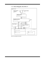
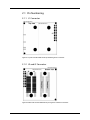
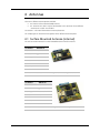
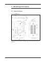
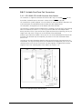
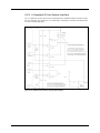
INDUSTRIAL BLUETOOTH™
OEM Serial Port Adapter™
2nd Generation
Electrical & Mechanical Datasheet
OEM Serial Port Adapter™
nd
2 Generation
Electrical & Mechanical Datasheet
Copyright © 2002-2003 connectBlue AB.
The contents of this document can be changed by connectBlue AB without prior notice
and do not constitute any binding undertakings from connectBlue AB. connectBlue AB
is not responsible under any circumstances for direct, indirect, unexpected damage or
consequent damage that is caused by this document.
All rights reserved.
Release: 2003-05
Document version: 1.5
Document number: cBProduct-0212-01
Printed in Sweden.
Trademarks
Registered trademarks from other companies are: Bluetooth is a trademark owned by
the Bluetooth SIG,Inc.Microsoft™, Windows™, Windows NT™,
Windows 2000™, Windows CE™, Windows ME™, are registered trademarks from
Microsoft Corporation.
Contents
1 Introduction
1.1
1.2
1.3
1.4
5
Related Documents.......................................................................... 5
Product Variants .............................................................................. 6
Block Diagram cB-0701-01 .............................................................. 7
Block Diagram cB-0702-01 .............................................................. 8
2 Electrical Interface and Connectors
2.1
2.2
2.3
2.4
2.5
2.6
9
Pin Numbering ............................................................................... 10
Pin Description............................................................................... 11
Characteristics ............................................................................... 14
Hardware Reset ............................................................................. 16
Logic Pins ...................................................................................... 16
Power Control ................................................................................ 16
3 Operating Status
17
4 Antennas
18
4.1
4.2
Surface Mounted Antenna (internal) .............................................. 18
Antennas on a Cable (external antennas) ...................................... 19
5 Mounting Information
5.1
5.2
5.3
5.4
5.5
5.6
22
Board Outlines ............................................................................... 22
Traces and Component Keep Out Area ......................................... 24
Using the J1 Pin Connector ........................................................... 25
Using the J2/J3 Board-to-Board Connectors.................................. 25
Using Press-Fit Nuts for Mounting the Module ............................... 28
Antenna Issues .............................................................................. 28
6 Bluetooth Information
29
7 Regulatory Information
30
7.1
7.2
Declaration of Conformity............................................................... 30
FCC Compliance............................................................................ 31
Appendix A A.1
A.2
Application Notes
34
Step-by-Step Guide........................................................................ 34
Design Examples ........................................................................... 36
Version 1.5 - 2003-05
4
1 Introduction
1.1 Related Documents
There are some documents related to the Serial Port Adapter (see Figure 1):
-
The Serial Port Adapter User Manual contains information on how to use the Serial Port
Adapter. Study this document before moving on to the others.
-
The Serial Port Adapter AT Commands document contains a description of the AT
commands supported in the Serial Port Adapter. It also contains information on how to use
the AT commands to create Bluetooth applications.
-
The OEM Serial Port Adapter Electrical & Mechanical Datasheet (this document)
contains important information about the OEM Serial Port Adapter. Read this document if
you are using the OEM Serial Port Adapter.
-
The Bluetooth Enabler Development Kit is required when using the ECI functionality
embedded in the Serial Port Adapter.
o
The ECI Driver with connectBlue Extensions User Manual contains a
description of the ECI functionality available in the Serial Port Adapter. It also
contains information on how to use the ECI Driver to create Bluetooth applications.
If you are going to use the ECI protocol in your application, study this document.
o
The ECI Specification and the ECI Specification with connectBlue Extensions
contain detailed descriptions of the ECI protocol. These documents should be used
as a reference when reading the ECI Driver with connectBlue Extensions User
Manual.
Serial Port Adapter
AT Commands
OEM Serial Port Adapter
Electrical & Mechanical Datasheet
Serial Port Adapter
User Manual
Bluetooth Enabler Development Kit
ECI Specification
ECI Driver with
connectBlue
Extensions
User Manual
ECI Specification with
connectBlue Extensions
Figure 1: Serial Port Adapter documents
Version 1.5 - 2003-05
5
1.2 Product Variants
This Electrical and Mechanical datasheet contains information about the second generation
OEM Serial Port Adapter. There are 4 different products (see Picture 1) based on two different
hardware modules cB-0701-01 and cB-0702-01. This document makes references to the OEM
Module ID, not the Product Name (see Table 1).
Table 1: Product variants
Product Name
OEM Module ID
Type
Description
OEMSPA13i
cB-0701-01
Class 2 / 0 dBm
OEM Serial Port Adapter
13i with internal antenna
OEMSPA13x
cB-0701-01
Class 2 / 0 dBm
OEM Serial Port Adapter
13x with external antenna
OEMSPA33i
cB-0702-01
Class 1 / 20 dBm
OEM Serial Port Adapter
33i with internal antenna
OEMSPA33x
cB-0702-01
Class 1 / 20 dBm
OEM Serial Port Adapter
33x with external antenna
1.2.1 cB-0701-01
cB-0701-01 is a small size Bluetooth module based on the Infineon (former Ericsson
Microelectronics) PBM 990 80 baseband controller and the PBA 313 05 (0dBm) radio.
The PBM 990 80 has on chip SRAM and FLASH stacked in the same package.
The product name is OEMSPA 13i/x, depending on whether an internal (i) or an external (x)
antenna is used.
1.2.2 cB-0702-01
cB-0702-01 is a long-range versatile Bluetooth module based on the Infineon (former Ericsson
Microelectronics) PBM 990 90 baseband controller and the PBA 313 02 (20dBm) radio.
The PBM 990 90 has on chip SRAM, the FLASH is located in a separate package. cB-0702-01
also contains external SRAM.
The product name is OEMSPA 33i/x, depending on whether an internal (i) or an external (x)
antenna is used.
Picture 1: The OEM Serial Port Adapter product family
Version 1.5 - 2003-05
6
1.3 Block Diagram cB-0701-01
Figure 2: Block diagram of cB-0701-01
Version 1.5 - 2003-05
7
1.4 Block Diagram cB-0702-01
Figure 3: Block diagram of cB-0702-01
Version 1.5 - 2003-05
8
2 Electrical Interface and Connectors
This section describes the signals available on the module interface connectors.
There are two ways to connect to the OEM Serial Port Adapter:
•
Via the J1 connector, a 2x10-pin 2mm pitch pin header.
•
Via the 1x20-pin 1mm pitch board-to-board (one piece part) connectors, J2 through J5.
NOTE! J4 and J5 are only available on cB-0702-01
The J2 to J5 connectors on the OEM Serial Port Adapter exist on the module only as a mating
PCB-layout pattern (see Picture 3).
Picture 2: J1 on the topside of cB-0701-01. The
same connector is available on cB-0702-01.
Picture 3: J2 to J5 pads of cB-0702-01, only J2 to J3
are available on cB-0701-01.
NOTE! Connectors J3 to J5 are for future use only and will not be covered in detail in
this document.
Version 1.5 - 2003-05
9
2.1 Pin Numbering
2.1.1 J1 Connector
Figure 4: Top view of the two PCBs with the pin numbering of the J1 connector.
2.1.2 J2 and J3 Connector
Figure 5: Bottom view of the two PCBs with the pinning of the J2 and the J3 connector.
Version 1.5 - 2003-05
10
2.2 Pin Description
2.2.1 J1 and J2 Connector
The J1 and the J2 connector has the same signal set-up and are internally connected, see Table
2.
Table 2: Signals on J1 and J2
J1&J2 Pin Name
Pin Nr
Signal Name
Signal
Level
Type
Description
1, 2
VSS
Ground
Ground
Pins internally connected.
3, 4
VCC_5V
Power
3.3V–6V
Pins internally connected.
If only cB-0701-01 is used the range
3.0V – 6.0V is allowed
5
RS232-CTS
Clear To Send
RS232
Input
6
RS232-TxD
Transmit Data
RS232
Output
7
RS232-RTS
Request To Send
RS232
Output
8
RS232-RxD
Receive Data
RS232
Input
9
RS232-DTR
Data Terminal Ready
RS232
Output
10
RS232-DSR
Data Set Ready
RS232
Input
Hardware flow control
Hardware flow control
Also used to control the power
saving mode “stop mode”.
See chapter 0 for more information.
11
RED/Mode
Red LED output and
serial interface mode
select input
CMOS
In/Out
This signal is multiplexed:
RED:
Logic Red LED Signal (see Chapter 3,
Table 8). Not valid until 500ms after
startup.
Mode:
The level on this pin during power
up selects RS232 (High) or logic
(Low) level UART-communication.
The Mode pin is only valid during
the first 500ms after startup and
cannot be changed during
operation.
The Mode pin is internally pulled up
i.e. RS232 mode is the default
setting. Recommended value of the
pull-down resistor is 10 kΩ.
See Section A.2.3.2 for design
examples.
Version 1.5 - 2003-05
11
J1&J2 Pin Name
Pin Nr
Signal Name
Signal
Level
Type
Description
12
Function switch
CMOS
In
Used for the “Connect on external
signal” function, see the Serial Port
Adapter User Manual for more
information on the Function switch.
Switch-0
See Section A.2.3.4 for design
examples.
13
GREEN/
Switch-1
Green LED output and
Restore switch
CMOS
In/Out
This signal is multiplexed:
GREEN:
Logic Green LED Signal (see Chapter
3, Table 8). Not valid until 500ms
after startup.
Switch-1:
If the level on this pin is set to Low
the units goes back to default serial
settings.
The “Restore Default” input is only
active during the first 500ms after
startup.
See the Serial Port Adapter User
Manual for more information on the
Restore switch.
See Section A.2.3.3 for design
examples.
14
BLUE
Blue LED output
CMOS
Output
Logic Blue LED Signal (see Chapter
3, Table 8).
See Section A.2.3.1 for design
examples.
1
15
UART1-CTS
16
1
Clear To Send
CMOS
Input
Hardware flow control. See Note 1
below.
UART1-TxD
Transmit Data
CMOS
Output
17
UART1-RTS
Request To Send
CMOS
Output
Hardware flow control.
18
UART1-RxD1
Receive Data
CMOS
Input
See Note 1 below.
19
UART1-DTR
Data Terminal Ready
CMOS
Output
20
UART1-DSR
Data Set Ready
CMOS
Input
Also used to control “stop down
mode”. See Section 0 for more
information.
Must be pulled-up (82kΩ) if not used in UART mode on cB-0701-01.
Version 1.5 - 2003-05
12
2.2.2 J3 Connector
The only pin available for use on the J3 connector is the RESET pin.
Table 3: Signals on J3
J3
Pin Nr
Pin Name
Signal Name
Signal
Level
Type
1-18, 20
19
Description
Reserved, do not connect.
RESET
Hardware reset
CMOS
Input
Active low. Must be open drain
collector.
See Section A.2.4 for design
examples.
2.2.3 J4 and J5 Connectors
These connectors are for future use and are not covered by this document.
Version 1.5 - 2003-05
13
2.3 Characteristics
The cB-0701-01 and cB-0702-01 boards are designed to be fully interchangeable. This is
possible if the host product has made space for the cB-0702-01 board. This makes it possible to
choose freely between a class 1 or class 2 device without any change of the host product.
There is only a small electrical different between the modules. The cB-0702-01 module has a
step-down switch mode power supply (SMTP) and the current consumption will decrease when
the supply voltage increases (constant power). The cB-0701-01 module has a linear power
supply, which means that the current is constant if the voltage supply is changed. This means
that the current will increase for the cB-0702-01 when the voltage supply decreases to 3.3V
compared to Table 5.
Table 4: Power supply
Symbol
Parameter
VCC_5V
Power supply
cB-0701-01
cB-0702-01
Unit
Min
3.0
3.3
V
Max
6.0
6.0
V
Current consumption depends on operating status, communication speed and load on RS232
pins etc (see Table 5).
An example:
Product used: OEMSPA13i (cB-0701-01)
Operating status of interest: Connected and transmitting data
Serial settings: RS232, 19.2kBits/s, no hardware flow control (only RxD and TxD connected)
Other end Transceiver: Receiver load = 3kΩ, Voltage levels: ±9V
Current consumption: 50I_Average + 7I_TxD + 9 / 20I_RxD = 57.45mA
Table 5: Current consumption
Symbol
Mode
cB-0701-01
≤57.6
Baud rate1
2
ICC
Not connected
Not
connected,
stop mode
enabled
Connected
25
60
18
40
mA
Peak
85
120
65
90
mA
Not connectable
Average
0.6
0.7
0.5
0.5
mA
Connectable
Average
1.1
1.5
0.6
1.0
mA
Connectable,
discoverable
Average
2.3
2.5
1
1.2
mA
Idle
Average
35
70
27
49
mA
100
150
170
210
mA
50
85
35
78
mA
100
150
170
210
mA
7
7
7
7
mA
20
20
20
20
kΩ
Transmitting
Average
Peak
RRS232 load
3
4
>57.6 ≤57.6 >57.6 kBits/s
Average
Peak
IRS232 Output
cB-0702-01 Unit
RS232
Average
RS232
Typ
1
The internal clock frequency increases when the baud rate is higher than 57.6kBits/s
@ VCC_5V = 5V
3
RS232 output signals TxD RTS, DTR loaded with 3kΩ. Not included in ICC, very dependent on the load.
4
Internal load on each RS232 input pin.
2
Version 1.5 - 2003-05
14
Table 6: Input/output signals
Symbol
Parameter
VIN Low
Logic LOW level input voltage
VIN High
cB-0701-01
Logic HIGH level input voltage
cB-0702-01
Unit
Min
-0.3
-0.3
V
Max
0.8
0.95
V
Min
2.05
2.25
V
Max
3.2
3.5
V
VOUT Low
Logic LOW level output voltage
Max
0.1
0.1
V
VOUT High
Logic HIGH level output voltage
Min
2.8
2.8
V
IGPIO
Sink and source current
Max
4
4
mA
CGPIO
Input capacitance
Typ
30
30
pF
CRESET
Reset input capacitance
Typ
20
20
nF
VT_OUT_RS232
RS232 Transmit output voltage
Typ
±6
±6
V
VR_IN_RS232
HIGH
RS232 HIGH level receive input voltage Min
(logic LOW)
Typ
3
3
V
6
6
V
Max
25
25
V
VR_IN_RS232 LOW RS232 LOW level receive input voltage Max
(logic HIGH)
Typ
-3
-3
V
-6
-6
V
Min
-25
-25
V
Table 7: Temperatures characteristics
Parameter
cB-0701-01
Storage temperature
Recommended operating temperature
Maximum operating temperature
Version 1.5 - 2003-05
cB-0702-01
Unit
Min
-40
-40
°C
Max
+85
+85
°C
Min
-20
-30
°C
Max
+75
+55
°C
Min
-30
-30
°C
Max
+75
+75
°C
15
2.4 Hardware Reset
A hardware RESET input is available on the J3 connector (see Section 2.2.2). An external reset
source must be open drain collector, see Section A.2.4 for design examples. The RESET pin is
pulled-up with 82kΩ.
2.5 Logic Pins
All logic input pins have protecting diodes to VSS and VCC (2.9V), see Figure 6 and Figure 7.
The UART-RxD and UART-CTS pins do not have internal pull-up resistors. When UART mode is
used, they must be defined, either by the host system UART or pulled-up (see Figure 8 for a 5V
system). If In RS232 mode is used, they can be left undefined.
The supply voltage must be powered on prior to or simultaneously to the logic pin voltages.
Figure 6: Logic pin design on cB-0701-01.
Figure 7: Logic pin design on cB-0702-01.
Use a resistive divider in a 5V system to set logic input pin to a HIGH state instead of a pull-up
resistor (see Figure 8).
Figure 8: Use a resistive divider instead of Pull-up in a 5V system.
2.6 Power Control
The DSR signal on the UART and the RS232 interfaces may be used to control “stop mode”.
“Stop mode” is the most efficient power saving mode.
For more information about “stop mode”, see the Serial Port Adapter User Manual.
Version 1.5 - 2003-05
16
3 Operating Status
The module can be in different modes (see the Serial Port Adapter User Manual for more
information about the modes) and the RED, GREEN and BLUE signals can be used to detect or
indicating the status, see Table 8. The LED signals are active LOW.
Table 8: Signal states in different module modes
Serial Port Adapter Mode
Status
RGB LED
Color
GREEN
GPIO
BLUE
GPIO
RED
GPIO
Data mode
IDLE
Green
LOW
HIGH
HIGH
AT mode, ECI mode
IDLE
Orange
LOW
HIGH
LOW
Data mode, AT mode, ECI mode
CONNECTING
Purple
HIGH
LOW
LOW
Data mode, AT mode, ECI mode
CONNECTED1
Blue
HIGH
LOW
HIGH
1
1
On data activity the active LEDs flashes and will be HIGH for 50-100ms. For information on how to suppress the flashes
see Section A.2.3.1.
Version 1.5 - 2003-05
17
4 Antennas
There are 2 different antenna options available:
•
An internal surface mounted (SMD) antenna.
•
An “antenna on a cable” may be connected to a U.FL connector. Three different
“antennas on a cable” are available.
See Section 5.1 for more information on antenna placement.
This chapter gives an overview of the qualities of the different antenna options.
4.1 Surface Mounted Antenna (internal)
The unit cannot be mounted in a metal-shielded enclosure with this antenna.
Part Number
OEMSPA 13i
Antenna name
Mica 2.4 GHz
Manufacture
gigaAnt
Antenna type
Patch antenna
Polarization
Linear
Gain
+2.7dBi
Size (LxWxH)
20.5x3.6x3.35 mm
Connector
Surface mounted
Comment
See Section 5.1 for mounting the module considering the antenna.
Part Number
OEMSPA 33i
Antenna name
Mica 2.4 GHz
Manufacture
gigaAnt
Antenna type
Patch antenna
Polarization
Linear
Gain
+2.7dBi
Size (LxWxH)
20.5x3.6x3.35 mm
Connector
Surface mounted
Comment
See Section 5.1 for mounting the module considering the antenna.
Version 1.5 - 2003-05
18
4.2 Antennas on a Cable (external antennas)
The external antennas are connected to the board through a U.FL connector. Some of the
antennas are connected directly to the U.FL connector of the board and some are connected
using an SMA connected through a short U.FL to SMA adapter cable.
4.2.1 Antenna Accessories
Part Number
cB-ACC-18
Name
U.FL to SMA
adapter cable
Connector
U.FL and
SMA female
Cable length
120 mm
Comment
The SMA connector may be mounted in a panel.
Version 1.5 - 2003-05
19
4.2.2 Antennas
Part Number
cB-ACC-16
Name
WCR-2400-SMA
Manufacture
Centurion
Type
½ wave dipole
Polarization
Vertical
Gain
+2.5dBi
Size
100 mm
Connector
SMA male
Comment
To be mounted on the U.FL to SMA adapter cable.
Part Number
cB-ACC-17
Name
Reel planTec
Bluetooth m70
Manufacture
Reel
Size (∅xH)
75x20 mm
Gain
+1dBi
Mounting
M16x13.6 mm
Cable length
3m
Connector
SMA male
Other info
Waterproof (IP67)
Comment
To be mounted on the U.FL to SMA adapter cable.
Version 1.5 - 2003-05
20
Part Number
cB-ACC-19
Name
CAP24235
Microblue
Manufacture
Centurion
Type
Microstrip
Polarization
Linear
Gain
+1.5dBi
Size
21x60 mm
Cable length
200 mm
Connector
U.FL
Comment
Connected directly to the U.FL connector on OEM board.
Part Number
cB-ACC-20
Name
CAF94146
Microsphere
Manufacture
Centurion
Type
Microstrip
Polarization
Linear
Gain
+2.7dBi
Size (LxWxH)
46x30x2.5 mm
Cable length
200 mm
Connector
U.FL or SMA
Comment
Connected directly to the U.FL connector on OEM board. Delivered with a
mounting kit.
Version 1.5 - 2003-05
21
5 Mounting Information
5.1 Board Outlines
5.1.1 cB-0701-01
Figure 9: cB-0701-01 dimensions [mm]. The J2 pads are longer to fit both the SEI and FSI connector (see
Section 5.4).
Version 1.5 - 2003-05
22
5.1.2 cB-0702-01
Figure 10: cB-0702-01 dimensions [mm]. The J2 pads are longer to fit both the SEI and FSI connector (see Section
5.4).
Version 1.5 - 2003-05
23
5.1.3 Mounting Holes
There are 2 x 2.3mm mounting holes on cB-0701-01 and 2 x 2.3mm, 2 x 2.0mm mounting
holes on cB-0702-01. The reasons for the 2.3mm holes are that the threaded M2 holes on the
FSI and the SEI connectors (see Section 5.4.1) are not aligned. The outer tangents of the 2.3mm
holes align the module if the FSI connector is used and the inner if SEI connector is used (see
Figure 11). The 2mm holes on cB-0702-01 are aligned with the FSI connector (see Figure 10).
Choose the outer tangent (CC distance 27.24mm) if the module is aligned and mounted with
some other technique based on M2 screws (e.g. press-fit nuts), see Figure 12 and Figure 13.
Figure 11: The 2.3mm mounting holes [mm]
5.2 Traces and Component Keep Out Area
The 20-pin 2 mm pitch pin connector (J1) sticks out 1.2 mm below the bottom side of the OEM
Serial Port Adapter boards.
It is recommended to keep traces and components out of this area on the motherboard or keep
a safe distance between the motherboard and the OEM Serial Port Adapter board (> 1.6 mm).
See Section 5.1 for detailed measurements and positions for the J1 connector.
Version 1.5 - 2003-05
24
5.3 Using the J1 Pin Connector
If you mount the boards on a motherboard using the mounting holes, distances higher or equal
to 1.6 mm must be used (due to the pins of the J1 connector, see Section 5.2).
Chapter 2 contains more information about the connector and the electrical interface.
5.3.1 Suitable Header Connectors
5.3.1.1 TCSD-10-D-XXX-01-F-N Flat Cable Connector from Samtec
The TCSD family is a 2mm pitch flat cable connector (including flat cable). The cable is available
with different connector options. See www.samtec.com for more information and your local
distributor.
Another manufacturer is AMP, www.amp.com.
5.4 Using the J2/J3 Board-to-Board Connectors
The board-to-board connector should be a 1mm pitch one-piece part connector. The
recommended manufacture is Samtec with many connector options available; see Section
5.4.1.1 and 5.4.1.2.
Chapter 2 contains more information about the connector and the electrical interface.
A tip is to make place for the J1 pin connector as indicated in Section 5.2. This allows you to use
a standard connectBlue OEM Serial Port Adapter even if you are not using a board-to-board
connector. Contact connectBlue if there is a requirement to use this reserved area for
components.
Version 1.5 - 2003-05
25
5.4.1 Suitable One-Piece Part Connectors
5.4.1.1 SEI-120-02-GF-S-M-AB Connector from Samtec
This connector is a single row connector and can be used if only J2 is needed ( RESET will not
be available, the double row FSI connector is a better choice if RESET is required).
This connector has a profile height of 1.65 mm and this has to be considered if components are
to be mounted on the motherboard under the OEM Serial Port Adapter board.
The –AB option is for alignment pin on the bottom side of the connector.
The connector is available with M2 threaded inserts (–M option in part no) that fit the mounting
holes on the board (see Section 5.1.3). You may screw the OEM Serial Port Adapter board
directly into these inserts. If you want to have a tighter and more secure mounting, you may use
longer screws and secure it using a nut on the backside of the motherboard.
Another way to mount the module is to use press-fit nuts on the motherboard and skip the M2
threads on the connector (skip the -M option), see Section 5.5 for more information about
press-fit nuts.
See Figure 12 for more information about the connector and necessary measurements on the
motherboard. The large mounting holes on the motherboard are designed for press-fit nuts and
could be smaller if press-fit nuts are not used. The mounting holes are aligned with the outer
tangent of the 2.3mm mounting holes of the module (see Section 5.1.3).
Figure 12: Host PCB layout [mm] for SEI-120-02-GF-S.
Version 1.5 - 2003-05
26
5.4.1.2 FSI-120-03-G-D-M-AB Connector from Samtec
This connector is a double row connector and can be used if both J2 and J3 are needed
( RESET is only available on J3).
This connector has a height of 3.0mm (-03 option) and this has to be considered if components
are to be mounted on the motherboard under the OEM Serial Port Adapter board. The
connector is also available with a height of 6.0mm and 10.0mm (-06 and –10 option).
The –AB option is for alignment pin on the bottom side of the connector.
The connector is available with M2 threaded inserts (–M option in part no) that fit the mounting
holes on the board (see Section 5.1.3). You may screw the OEM Serial Port Adapter board
directly into these inserts. If you want to have a tighter and more secure mounting you may use
longer screws and secure it using a nut on the backside of the motherboard.
Another way to mount the module is to use press-fit nuts on the motherboard and skip the M2
threads on the connector (skip the -M option), see Section 5.5 for more information about
press-fit nuts.
See Figure 13 for more information about the connector and necessary measurements on the
motherboard. The large mounting holes on the motherboard are designed for press-fit nuts and
could be smaller if press-fit nuts are not used (see Section 5.1.3).
Figure 13: Host PCB layout [mm] for FSI-120-XX-GF-S.
Version 1.5 - 2003-05
27
5.5 Using Press-Fit Nuts for Mounting the Module
A press-fit nut is pressed into the PCB from the bottom side with a special press tool. M2 sized
press-fit nuts are suitable for the modules (see Figure 12 and Figure 13) and are manufactured
by PEM Fastening Systems (www.pemnet.com), part no KFS2-M2 (see Figure 14). Be careful
with the distance between the nuts regarding alignment, see Section 5.1.3.
Figure 14: KFS2-M2 press-fit nut.
Spacer-pipes are recommended to use between the PCBs when press-fit nuts are used.
Press-fit nuts are used on the OEM Module Adapter (included in the connectBlue complete kits).
5.6 Antenna Issues
The unit cannot be mounted arbitrary, because of the radio communication. The unit with an
internal surface mounted antenna (OEMSPA13i and OEMSPA33i) cannot be mounted in a metal
enclosure.
If a metal enclosure is required, one of the external antenna options has to be used. See Section
4.2 for more information on the antenna options available.
A recommended space around the SMD antenna
must be free from wires, circuits or other conductive
components of the user application.
Illustration of a user
application
OEM Serial Port Adapter
Figure 15: Internal antenna mounting instruction [mm].
Version 1.5 - 2003-05
28
6 Bluetooth Information
In the tables below you can find information about Bluetooth properties.
Table 9: Bluetooth information cB-0701-01
Parameter
Data
Bluetooth radio
Infineon/Ericsson PBD 313 05 (RAN)
Bluetooth base band controller
Infineon/Ericsson PBM 990 80 (FLINK)
RF output power
Class 2, typ 1.5dBm
Receive sensitive level
-80dBm (0.1% BER)
Receive input level (max)
Max +14 dBm
Output frequency
2.402 –2.480 GHz, ISM band.
Point to multi-point operation
Yes
Bluetooth stack
Embedded host stack
Bluetooth qualification
1.1
Table 10: Bluetooth information cB-0702-01
Parameter
Data
Bluetooth radio
Infineon/Ericsson PBD 313 02 (MIRIAN)
Bluetooth base band controller
Infineon/Ericsson PBM 990 90 (BLINK)
RF output power
Class 1, min –28dBm, max +16dBm
Receive sensitive level
-80dBm (0.1% BER)
Receive input level (max)
Max +15 dBm
Output frequency
2.402 –2.480 GHz, ISM band.
Point to multi-point operation
Yes
Bluetooth stack
Embedded host stack
Bluetooth qualification
1.1
Version 1.5 - 2003-05
29
7 Regulatory Information
7.1 Declaration of Conformity
We, connectBlue AB, of
Stora Varvsgatan 11 N:1
SE-211 19 Malmö, Sweden
declare under our sole responsibility that our products:
OEM Serial Port Adapter 13i, cB-0032-01, OEM Serial Port Adapter 13x, cB-0033-01
OEM Serial Port Adapter 33i, cB-0034-01, OEM Serial Port Adapter 33x, cB-0035-01
Serial Port Adapter 12i, cB-0036-01, Serial Port Adapter 32i, cB-0037-01
Serial Port Adapter 33i, cB-0041-01, Serial Port Adapter 33c, cB-0038-01
Rugged Serial Port Adapter 32s, cB-0039-01, OEM Module Adapter 2, cB-0040-01
to which this declaration relates, conforms to the following product specifications:
R&TTE Directive 1999/5/EC
EN 300 328-2 V1.1.1 (2000-07)
EMC Directive: 89/336/EEC
EN 301 489-1 V1.3.1 (2001-09)
EN 301 489-17 V1.1.1 (2000-09)
EN 61000-6-2 (1999)
Low Voltage Directive: 73/23/EEC
EN 61131-2
Medical Electrical Equipment
IEC 60601-1-2
A notification must be made to each of the national authorities responsible for radio spectrum
management of the intention to place radio equipment that uses frequency bands whose use
is not harmonized throughout the EU, on its national market.
More information at: http://europa.eu.int/comm/enterprise/rtte/gener.htm
Version 1.5 - 2003-05
30
7.2 FCC Compliance
7.2.1 FCC Statement for cB-0701-01
This device complies with Part 15 of the FCC Rules. Operation is subject to the following two
conditions: (1) this device may not cause harmful interference, and (2) this device must accept
any interference received, including interference that may cause undesired operation.
NOTE: This equipment has been tested and found to comply with the limits for a Class B digital device,
pursuant to Part 15 of the FCC Rules. These limits are designed to provide reasonable protection
against harmful interference in a residential installation. This equipment generates, uses and can
radiate radio frequency energy and, if not installed and used in accordance with the
instructions, may cause harmful interference to radio communications. However, there is no
guarantee that interference will not occur in a particular installation. If this equipment does
cause harmful interference to radio or television reception, which can be determined by turning
the equipment off and on, the user is encouraged to try to correct the interference by one or
more of the following measures:
•
Reorient or relocate the receiving antenna
•
Increase the separation between the equipment and receiver
•
Connect the equipment into an outlet on a circuit different from that to which the receiver
is connected
•
Consult the dealer or an experienced radio/TV technician for help
7.2.1.1 Labeling Requirements for End Product
For an end product using the OEM Serial Port Adapter or the OEM Bluetooth Enabler there must
be a label containing, at least, the following information:
This device contains
FCC ID: PVH070101
The label must be affixed on an exterior surface of the end product such that it will be visible
upon inspection in compliance with the modular approval guidelines developed by the FCC.
In addition, the user manual for the end product must contain the following information:
“This device complies with Part 15 of the FCC Rules. Operation is subject to the following two
conditions: (1) this device may not cause harmful interference, and (2) this device must accept
any interference received, including interference that may cause undesired operation.”
7.2.1.2 Antenna
When using the module equipped with the external antennas as described previously the
antenna is fixed and cannot be removed or replaced by the end user.
7.2.1.3 Caution
Any changes or modifications NOT explicitly APPROVED by connectBlue AB could cause the
module to cease to comply with FCC rules part 15, and thus void the user’s authority to operate
the equipment.
Version 1.5 - 2003-05
31
7.2.2 FCC Statement for cB-0702-01
This device complies with Part 15 of the FCC Rules. Operation is subject to the following two
conditions: (1) this device may not cause harmful interference, and (2) this device must accept
any interference received, including interference that may cause undesired operation.
NOTE: This equipment has been tested and found to comply with the limits for a Class B digital device,
pursuant to Part 15 of the FCC Rules. These limits are designed to provide reasonable protection
against harmful interference in a residential installation. This equipment generates, uses and can
radiate radio frequency energy and, if not installed and used in accordance with the
instructions, may cause harmful interference to radio communications. However, there is no
guarantee that interference will not occur in a particular installation. If this equipment does
cause harmful interference to radio or television reception, which can be determined by turning
the equipment off and on, the user is encouraged to try to correct the interference by one or
more of the following measures:
•
Reorient or relocate the receiving antenna
•
Increase the separation between the equipment and receiver
•
Connect the equipment into an outlet on a circuit different from that to which the receiver
is connected
•
Consult the dealer or an experienced radio/TV technician for help
7.2.2.1 Labeling Requirements for End Product
For an end product using the OEM Serial Port Adapter or the OEM Bluetooth Enabler there must
be a label containing, at least, the following information:
This device contains
FCC ID: PVH070201
The label must be affixed on an exterior surface of the end product such that it will be visible
upon inspection in compliance with the modular approval guidelines developed by the FCC.
In addition, the user manual for the end product must contain the following information:
“This device complies with Part 15 of the FCC Rules. Operation is subject to the following two
conditions: (1) this device may not cause harmful interference, and (2) this device must accept
any interference received, including interference that may cause undesired operation.”
7.2.2.2 RF-exposure Statement for cB-0702-01
This portable modular transmitter MUST have a separation distance of at least 2.5cm between
the antenna and the body of the user or nearby persons, excluding hands, wrists, feet, and
ankles.
If the radio module is installed in a laptop display, transmission MUST be prevented if the lid is
closed to ensure that the minimum distance of 2.5cm between the user and the transmitting
antenna is maintained.
Any notification to the end user of installation or removal instructions about the integrated
radio module is NOT allowed.
Version 1.5 - 2003-05
32
7.2.2.3 Antenna
When using the module equipped with the external antennas as described previously the
antenna MUST be fixed, not to be able to be removed or replaced by the end user.
On modules equipped with SMA-connector, the connector-antenna thread MUST be locked
with LOCTITE ® Product 270.
LOCTITE ® Product 270 is a single component anaerobic glue. The product cures when
confined in the absence of air between close fitting metal surfaces.
7.2.2.4 Caution
Any changes or modifications NOT explicitly APPROVED by connectBlue AB could cause the
module to cease to comply with FCC rules part 15, and thus void the user’s authority to operate
the equipment.
Version 1.5 - 2003-05
33
Appendix A - Application Notes
Usually only a subset of the available functionality is of interest to the designer. In addition,
depending on the host system, the electrical interface can be designed in many ways. The
designer can use the step-by-step guide in this chapter as an aid in the design process.
A.1 Step-by-Step Guide
Table 11: Step-by-step guide with Yes and No answers.
Question
Yes
No
Do you wish to make your design
compatible with both the cB-0701-01
and the cB-0702-01 module?
The PCB outlines are larger on the Go on to next point.
cB-0702-01 module, which have to
be considered if high components
are placed near the module (see
Chapter 5).
There is a little variation in the
Voltage power supply and logic
levels between the modules and
the cB-0702-01 has higher peak
current consumption because of
higher output power (see Section
2.3).
Are you going to integrate the OEM
Serial Port Adapter in a metal
enclosure?
The internal antenna models
cannot be used. Use the
OEMSPA13x or OEMSPA33x.
You are free to choose
between the products. The
internal antenna models are
lower cost and are easier to
design-in. However, an
external antenna could give
better range.
Do you wish to use logic level (UART
mode) when communicating with the
OEM Serial Port Adapter?
See Section A.2.1.2 for electrical
design.
See Section A.2.1.1 for
electrical design.
Are you using a 5V host system?
See Section A.2.2, Figure 20 for
electrical design.
See Section A.2.2, Figure
19 for electrical design.
Is low power consumption important?
The power consumption can be
reduced by enabling the stop
mode, see Table 5. The stop mode
is controlled with the DSR pin, see
Section 0.
Go on to next point.
Do you wish to connect LEDs to the
OEM Serial Port Adapter?
See Section A.2.3 for design
examples for connecting the LEDs.
Go on to next point.
Do you want to detect the status of
the module with a controller?
See Chapter 3, Table 8 for status
detection and Section A.2.3 for
electrical design.
Go on to next point.
Do you wish to utilize the restore
switch?
See Section A.2.3.3 for electrical
design.
Go on to next point.
Version 1.5 - 2003-05
34
Question
Yes
No
Do you wish to utilize the Function
See Section A.2.3.4 for electrical
switch (“Connect on external signal”)? design.
Go on to next point.
Do you want to manually reset the
module?
Go on to next point.
See Section A.2.4 for electrical
design. Use the FSI connector, see
Section 5.4.1.2.
Version 1.5 - 2003-05
35
A.2 Design Examples
This section contains design examples for all interfaces on J1, J2 and J3. J1 and J2 have the
same pin set-up and are internally connected. You can use J1 or J2 depending on which
connector (see Section 5.1) you are using.
A.2.1 Serial Interface UART/RS232
The serial interface can operate in RS232 or UART mode, see Section A.2.3.2.
CTS (Clear To Send) and RTS (Request To Send) are used for hardware flow control.
DSR (Data Set Ready) is used to control power saving functions, see Section 2.6.
DTR (Data Terminal Ready) can be used to detect if the module is up and running and ready to
receive data.
Note! The module must be configured to flow control none if hardware flow control is
not used, see the Serial Port Adapter User Manual.
A.2.1.1 RS232 Mode
The modules are fully compatible with the EIA-232 standard and can be connected to all RS232
transceivers. Speed and current consumption depends on the host system RS232 transceiver.
See Figure 16 for a complete example. Not used functionality can be left unconnected; see
Section A.2.1.
Figure 16: A complete RS232 interface.
Version 1.5 - 2003-05
36
A.2.1.2 UART Mode
Logic levels (see Table 6) are used in UART mode; see Section A.2.3.2 for information on how to
select UART mode.
Note! It is very important to set the module in UART mode properly when interfacing
with logic levels; collision with the internal RS232 transceiver could damage the
module.
UART mode can be used in a host controller application with a UART interface. The design of
the interface depends on the power supply voltage of the host system; see Figure 17 for a
3.0/3.3V host system and Figure 18 for a 5V host system. CTS and RxD must be pulled-up
(82kΩ) if not used, other signals not used can be left unconnected; see Section A.2.1.
Figure 17: A complete UART interface with a
3.0/3.3V host system.
Figure 18: A complete UART interface with a 5V host
system.
Version 1.5 - 2003-05
37
A.2.2 Logic Levels
A 3.0/3.3V host system can be connected directly to the logic level pins (BLUE, UART1-TxD /
UART1-RxD etc). A serial 100Ω resistor shall be used (see Figure 19) for protection, see Table 6
for logic levels characteristics.
A 5V host system can easily be adjusted to the logic levels. A host system output signal can use
a resistive divider (18k/22k) to adjust the levels. This is applicable for speeds up to 115.2kBits/s.
The divider can be adjusted to 1.8k/2.2k and a logic buffer (74HCT08) for higher speeds (see
Figure 20). The host system input pins could require a buffer (see Figure 20) depending on the
logic level requirements (see Table 6).
The 74HCT08 gate is also available in a single gate package (74AHCT1G08).
Figure 19: Logic levels interface to a 3/3.3V
system. A protective 100Ω resistor is used.
Figure 20: Interface example with logic levels to a 5V
system.
A 5V system with open collector outputs is designed in Figure 21.
Figure 21: Open collector outputs.
Version 1.5 - 2003-05
38
A.2.3 LED and Switch Design
A.2.3.1 BLUE Signal
The BLUE signal is not multiplexed with any other functionality, which makes the design more
straightforward (for more information see Figure 22). There are two important notes:
-
A blue LED requires about 3.5V forward voltage drop (cannot be used in a 3.3V system).
-
The BLUE signal can be used to detect if the module is connected or not. The BLUE signal
flashes when the module is sending and receiving data (see Chapter 3, Table 8). See Figure
23 for an example on how to suppress the flashes.
Figure 22: A blue LED can be connected directly to the module if the LED current is below 4mA. A high
state (active low) makes the voltage drop over the LED to 2.2V. This is not enough to light the LED.
Figure 23: A Low pass filter and a 74HC08 suppress the flashes when the module is sending and receiving
data. The Blue LED can be removed if not required.
Version 1.5 - 2003-05
39
A.2.3.2 RED/Mode Signal
The RED/Mode signal is a multiplexed signal:
-
RED - Logic red LED signal (see Chapter 3, Table 8). Becomes valid 500ms after start up.
-
Mode - The module reads the status of the signal during startup to decide if the serial
interface shall be RS232 (HIGH) or logic UART (LOW) levels. The input signal must be stable
for the first 500ms after startup (after reset/power on reset).
The signal is internally pulled-up (82kΩ) to 2.8V for RS232 as default.
If a LED is used in UART mode a high impendence buffer is required to prevent the signal from
being pulled-up via the LED. A 74HC08 logic gate can be used in a 3/3.3V system (see Figure
24) and a 74HCT08 logic gate in a 5V system (see Figure 25). Both gates are available in a single
gate package (74AHC1G08/74AHCT1G08).
Figure 24: UART mode selected together with
a red LED in a 3.3V host system. The status of
the signal can also be used as input to a host
controller.
Figure 25: UART mode selected together with
a red LED in a 5V host system. The status of
the signal can also be used as input to a host
controller.
The buffer can be removed in a 3.3V system if RS232 mode is used (see Figure 26).
In a 5V system the high state output (2.8V) from the module is not enough to turn off the LED
so a 74HCT08 buffer can be used to raise the high level to 5V (see Figure 27).
The 74HCT08 gate is available in a single gate package (74AHCT1G08).
Figure 26: RS232 mode selected (default) together
with a red LED in a 3.3V host system. The status of
the signal can also be used as input to a host
controller.
Figure 27: RS232 mode selected (default)
together with a red LED in a 5V host system.
The status of the signal can also be used as
input to a host controller.
Only a pull-down on the RED/Mode pin is needed if UART mode is used but no red LED is
required (see Figure 28). The RED/Mode pin can be left unconnected if RS232 (default) is used
and no red LED required.
Version 1.5 - 2003-05
40
Figure 28: The mode pin is pulled-down (10kΩ) in UART mode.
A.2.3.3 GREEN/Switch-1 signal
The GREEN/Switch-1 signal is a multiplexed signal:
-
GREEN - Logic green LED signal (see Chapter 3, Table 8). Becomes valid 500ms after start
up.
-
Switch-1 - The module reads the status of the signal at startup to decide if the serial
interface settings shall be restored (LOW) (see the Serial Port Adapter User Manual for
more details). The input signal must be stable for the first 500ms after startup (after
reset/power on reset).
The signal is internally pulled-up (82kΩ) to 2.8V for NOT restoring settings to default.
If a LED is used and a switch is required to be able to restore the settings, a high impendence
buffer need to prevent the signal from being pulled-up via the LED. A 74HC08 logic gate can be
used in a 3/3.3V system (see Figure 29) and a 74HCT08 logic gate in a 5V system (see Figure
30).
Both gates are available in a single gate package (74AHC1G08/74AHCT1G08).
Sometimes, over time, switch contacts can get an oxide layer. This may cause the closed switch
resistance to become too high to sink the signal to logic LOW (the signal is internally pulled-up
to 82kΩ). A design that prevents this can be found in Figure 34.
Figure 29: Switch-1 used together with a
green LED in a 3.3V host system. The status
of the signal can also be used as input to a
host controller. Notice the 10kΩ serial
resistor.
Figure 30: Switch-1 used together with a green
LED in a 5V host system. The status of the
signal can also be used as input to a host
controller. Notice the 10kΩ serial resistor.
The buffer can be removed in a 3.3V system if no restore switch is required (see Figure 31).
In a 5V system the high state output (2.8V) from the module is not enough to turn off the LED,
so a 74HCT08 buffer can be used to raise the high level to 5V (see Figure 32).
The 74HCT08 gate is also available in a single gate package (74AHCT1G08).
Version 1.5 - 2003-05
41
Figure 31: No restore switch used but a green
LED in a 3.3V host system. The status of the
signal can also be used as input to a host
controller.
Figure 32: No restore switch used but a green
LED in a 5V host system. The status of the
signal can also be used as input to a host
controller.
A serial resistor to the restore switch must be used to prevent a short circuit when the
GREEN/Switch-1 pin is in output HIGH state and the switch is pressed (see Figure 33).
Sometimes, over time, switch contacts can get an oxide layer. This may cause the closed switch
resistance to become too high to sink the signal to logic LOW (the signal is internally pulled-up
to 82kΩ). A design that prevents this can be found in Figure 34.
The GREEN/Switch-1 pin can be left unconnected if none of its functionality is required.
Figure 33: A low resistance restore switch
used. Notice the 10kΩ serial resistor.
Figure 34: If the resistance in the switch is not
guaranteed to be low enough, a safer design
can be used. Notice the 10kΩ serial resistor.
A.2.3.4 Switch-0 Signal
Switch-0 is not multiplexed with other functionality and a switch is easily implemented (see
Figure 35). Sometimes, over time, switch contacts can get an oxide layer. This may cause the
closed switch resistance to become too high to sink the signal to logic LOW (the signal is
internally pulled-up to 82kΩ). A design that prevents this can be found in Figure 36.
The Switch-0 pin can be left unconnected if its functionality is not used.
Figure 35: A low resistance function switch
used.
Figure 36: If the resistance in the switch is not
guaranteed to be low enough, a safer design
can be used.
Version 1.5 - 2003-05
42
A.2.4 Reset
The RESET pin can be connected to an external reset source, see Figure 37 for a switch
example.
If the reset signal is connected to an output signal it must be a open drain collector, see Figure
38. Notice the capacitive load on the RESET pin in Table 6, Section 2.3.
The RESET pin can be left unconnected if not used.
Figure 37: A reset switch.
Figure 38: Design of an open collector reset
from an active high output.
Version 1.5 - 2003-05
43
A.2.5 A Complete 5V Host System Interface
This is a complete 5V host system interface example with an RGB LED and two switches (except
the serial interface, see Section A.2.1 for information). The design is based on the LM339 Quad
OP-amp instead of logic gates.
Figure 39: A complete 5V host interface with operational amplifier
Version 1.5 - 2003-05
44