1
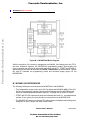
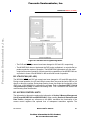
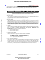
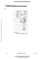
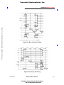
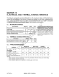
Freescale Semiconductor, Inc.
REV2.2 (11/02/99)
APPENDIX B
MC68EC040
Freescale Semiconductor, Inc...
NOTE
Rev. 2.2 contains timing information for 40 MHz operation.
Refer to chang bars. Some TBD values will be filled in shortly.
All references to MC68EC040 also apply to the MC68EC040V.
Refer to Appendix C MC68040V and MC68EC040V for more
information on the MC68EC040V.
The MC68EC040 is Motorola's third generation of M68000-compatible, high-performance,
32-bit microprocessors. The MC68EC040 is an embedded controller employing a highly
integrated architecture to provide very high performance in a monolithic HCMOS device. The
MC68EC040 integrates an MC68040-compatible integer unit, an access control unit (ACU),
and independent 4-Kbyte instruction and data caches. A six-stage instruction pipeline, multiple internal buses, and a full internal Harvard architecture, including separate caches for
both instruction and data accesses, provides a high degree of instruction execution parallelism. The inclusion of on-chip bus snooping logic, which directly supports cache coherency
in multimaster applications, enhances cache functionality.
The MC68EC040 is user-object-code compatible with previous members of the M68000
family and is specifically optimized to reduce the execution time of compiler-generated code.
The MC68EC040 is pin compatible with the MC68040 and MC68LC040. The MC68EC040
is implemented in Motorola's latest HCMOS technology, providing an ideal balance between
speed, power, and physical device size. Figure B-1 provides a simplified block diagram of
the MC68EC040.
The main features of the MC68EC040 include:
• MC68040-Compatible Integer Execution Unit
• 4-Kbyte Instruction Cache and 4-Kbyte Data Cache Accessible Simultaneously
• 32-Bit, Nonmultiplexed External Address and Data Buses with Synchronous Bursting
Interface
• User-Object-Code Compatible with All M68000 Microprocessors
• Concurrent Integer Unit, ACU, and Bus Controller Operation Maximizes Throughput
• Low-Latency Bus Accesses for Reduced Cache-Miss Penalty
• Multimaster/Multiprocessor Support via Bus Snooping
• 4-Gbyte Direct Addressing Range
MOTOROLA
M68040 USER’S MANUAL
For More Information On This Product,
Go to: www.freescale.com
B-1
Freescale Semiconductor, Inc.
Freescale Semiconductor, Inc...
MC68EC040 REV2.2 (11/02/99)
Figure B-1. MC68EC040 Block Diagram
With the exception of the memory management unit (MMU), the floating-point unit (FPU),
and their respective registers, the MC68EC040 programming model, data formats and
types, instruction set (except all instructions beginning with an “F”, PTEST, and PFLUSH),
and caches are the same as described in Section 1 Introduction for the MC68040. Figures
B-2 and B-3 illustrate the programming model and functional signal groups for the
MC68EC040.
B.1 MC68EC040 DIFFERENCES
The following differences exist between the MC68EC040 and MC68040:
• Two independent access control units (ACUs) replace the MC68040 MMUs. The ACU
has four corresponding registers (access control registers) that the MC68040 implements as data transparent translation registers. The page size is fixed at 4 Kbytes.
• PTEST and PFLUSH instructions cause an indeterminate result (i.e., an undetermined
number of bus cycles); the user should not execute them on the MC68EC040.
• The MC68EC040 does not contain an FPU which causes unimplemented floating-point
exceptions to occur using a new stack frame format.
B-2
M68040 USER’S MANUAL
For More Information On This Product,
Go to: www.freescale.com
MOTOROLA
Freescale Semiconductor, Inc.
Freescale Semiconductor, Inc...
MC68EC040 REV2.2 (11/02/99)
Figure B-2. MC68EC040 Programming Model
• The DLE and MDIS pin names have been changed to JS0 and JS1, respectively.
• The MC68EC040 does not implement the DLE mode, multiplexed, or output buffer impedance selection modes of operation. The MC68EC040 implements only the small
output buffer mode of operation. All timing and drive capabilities of the MC68EC040 are
equivalent to those of the MC68040 in the small buffer mode of operation.
B.2 JTAG SCAN (JS1–JS0)
The MC68040 MDIS and DLE pin names have been changed to JS1 and JS0 respectively.
During normal operation, the JS1 and JS0 pin cannot float, they must be tied to GND or Vcc
directly or through a resistor. During board testing, these pins retain the functionality of the
JTAG scan of the MC68040 for compatibility purposes. Refer to Section 6 IEEE 1149.1A
Test Access Port (JTAG) for details concerning IEEE 1149.1 Standard Test Access Port
and Boundary Scan Architecture.
B.3 ACCESS CONTROL UNITS
The information in this section replaces the information in Section 3 Memory Management
Unit (Except MC68EC040 and MC68EC040V). When reading Section 4 Instruction and
Data Caches, disregard any references to the MMU; remember the functionality of the
access control registers has replaced that of transparent translation registers. The
MOTOROLA
M68040 USER’S MANUAL
For More Information On This Product,
Go to: www.freescale.com
B-3
Freescale Semiconductor, Inc.
Freescale Semiconductor, Inc...
MC68EC040 REV2.2 (11/02/99)
Figure B-3. MC68EC040 Functional Signal Groups
MC68EC040 contains two independent ACUs, one for instructions and one for data. Each
ACU allows memory selections to be made requiring attributes particular to peripherals,
shared memory, or other special memory requirements. The following paragraphs describe
the ACUs and the access control registers contained in them.
B.3.1 Access Control Registers
Each ACU has two independent access control registers (ACRs). The instruction ACU contains the instruction access control registers (IACR0 and IACR1). The data ACU contains
the data access control registers (DACR0 and DACR1). Both ACRs provide and control status information for access control of memory in the MC68EC040. Only programs that execute in the supervisor mode using the MOVEC instruction can directly access the ACRs.
The 32-bit ACRs each define blocks of MC68EC040:address space for access control.
These blocks of address space can overlap or be separate, and are a minimum of 16
Mbytes. Three blocks are used with two user-defined attributes, cachability control and
optional write protection. The ACRs specify a block of address space as serialized noncachable for peripheral selections and as write-through for shared blocks of address space in
multi-processing applications. The ACRs can be configured to support many embedded
B-4
M68040 USER’S MANUAL
For More Information On This Product,
Go to: www.freescale.com
MOTOROLA
Freescale Semiconductor, Inc.
MC68EC040 REV2.2 (11/02/99)
control applications while maintaining cache integrity. Refer to Section 4 Instruction and
Data Caches for details concerning cachability. Figure B-4 illustrates the ACR format.
31
24 23
LOGICAL ADDRESS BASE
16 15 14 13 12 11 10
LOGICAL ADDRESS MASK E
S
0
0
0
9
8
U1 U0
7
0
6
5
CM
4
3
2
1
0
0
0
W
0
0
Figure B-4. MC68EC040 Access Control Register Format
Freescale Semiconductor, Inc...
ADDRESS BASE
This 8-bit field is compared with physical address bits A31–A24. Addresses that match in
this comparison (and are otherwise eligible) are accessible.
ADDRESS MASK
This 8-bit field contains a mask for the ADDRESS BASE field. Setting a bit in the ADDRESS MASK field causes the processor to ignore the corresponding bit in the ADDRESS BASE field. Setting some of the ADDRESS MASK bits to ones obtains blocks of
memory larger than 16 Mbytes. The low-order bits of this field are normally set to define
contiguous blocks larger than 16 Mbytes, although contiguous blocks are not required.
E—Enable
This bit enables and disables transparent translation of the block defined by this register.
Refer to Section 3 Memory Management Unit (Except MC68EC040 and
MC68EC040V) for details on transparent translation.
0 = Access control disabled.
1 = Access control enabled.
S—Supervisor/User Mode
This field specifies the way FC2 is used in matching an address:
00 =Match only if FC2 = 0 (user mode access).
01 =Match only if FC2 = 1 (supervisor mode access).
10, 11 =Ignore FC2 when matching.
U1, U0—User Page Attributes
These two bits drive on the user page attribute signals (UPA1 and UPA0). If an external
bus transfer results from the access, U0 and U1 are echoed to the UPA0 and UPA1
signals, respectively. The user can program these bits to support extended addressing,
bus snooping, or other applications. The MC68EC040 does not interpret these bits.
MOTOROLA
M68040 USER’S MANUAL
For More Information On This Product,
Go to: www.freescale.com
B-5
Freescale Semiconductor, Inc.
MC68EC040 REV2.2 (11/02/99)
Freescale Semiconductor, Inc...
CM—Cache Mode
This field selects the cache mode and access serialization for a page as follows:
00 = Cachable, Write-through
01 = Cachable, Copyback
10 = Noncachable, Serialized
11 = Noncachable
Detailed information on caching modes is available in Section 4 Instruction and Data
Caches, and information on serialization is available in Section 7 Bus Operation.
W—Write Protect
This bit indicates if the transparent block is write protected. If set, write and read-modify-write accesses are aborted as if the R-bit in a table descriptor were clear. Refer to 3.2.2
Descriptors for a description of table descriptors.
0 = Read and write accesses permitted.
1 = Write accesses not permitted.
B.3.2 Address Comparison
The following description of address comparison assumes that the ACRs are enabled.
Clearing the E-bit in each ACR independently disables access control, causing the processor to ignore it.
When an ACU receives a physical address, the privilege mode and the eight high-order bits
of the address are compared to the block of addresses defined by the two ACRs for the corresponding ACU. Each block of address space for an ACR contains an S-field, a BASE
ADDRESS field, and an ADDRESS MASK field. The S-field allows for matching either user
or supervisor accesses (or both). Setting a bit in the ADDRESS MASK field causes the corresponding bit of the ADDRESS BASE to be ignored in the address comparison and privilege mode. Setting successively higher order bits in the ADDRESS MASK field increases
the size of the block of address space.
The address for the current bus cycle and an ACR address match when the privilege mode
and address bits for each (not including the masked bits) are equal. Each ACR specifies
write protection for the block of address space. Enabling write protection for a block of
address space causes the abortion of write or read-modify-write accesses to the block, and
an access error exception occurs.
By appropriately configuring an ACR, flexible mappings can be specified. For example, to
control access to the user address space, the S-field equals $0, and the ADDRESS MASK
field equals $FF in all four ACRs. To control access to the supervisor address space
($00000000–$0FFFFFFF) with write protection, the BASE ADDRESS field = $0X, the
ADDRESS MASK field equals $0F, the W-bit is set to one, and the S-field = $1. The inclusion
of independent ACRs in both the instruction ACU (IACU) and data ACU (DACU provides an
exception to the merged instruction and data address space, allowing different access control for instruction and operand accesses. Also, since the instruction memory unit is only
used for instruction prefetches, different instruction and data ACRs can cause PC relative
operand fetches to be translated differently from instruction prefetches.
B-6
M68040 USER’S MANUAL
For More Information On This Product,
Go to: www.freescale.com
MOTOROLA
Freescale Semiconductor, Inc.
MC68EC040 REV2.2 (11/02/99)
Matching either of the ACRs in a corresponding ACU during an access to a memory unit
completes the access with the ACU. If both registers match, the access uses the xACR0 status bits. Addresses are passed through without translation if there is no match in the ACRs
and no table search occurs. The MC68EC040 does not perform table searches.
B.3.3 Effect of RSTI on the ACU
When the assertion of the reset input (RSTI) signal resets the MC68EC040, the E-bits of the
ACRs are cleared, disabling address access control.
Freescale Semiconductor, Inc...
B.4 SPECIAL MODES OF OPERATION
This part of the M68040 User's Manual does not apply to the MC68EC040. The
MC68EC040 does not sample the IPL2–IPL0, CDIS, JS0 (DLE on the MC68040), or JS1
(MDIS on the MC68040) pins on the rising edge of RSTI.
An external device asserts RSTI to reset the processor. When power is applied to the system, external circuitry should assert RSTI for a minimum of 10 BCLK cycles after VCC is
within tolerance. Figure B-5 is a functional timing diagram of the power-on reset operation,
illustrating the relationships between VCC, RSTI, and bus signals. The BCLK and PCLK
clock signals are required to be stable by the time VCC reaches the minimum operating specification. RSTI is internally synchronized for two BCLKS before being used, and must meet
the specified setup and hold times to BCLK (specifications #51 and #52 in MC68EC040
Electrical Characteristics) only if recognition by a specific BCLK rising edge is required.
Once RSTI is negated, the processor is internally held in reset for another 128 clock cycles.
During the reset period, all three-statable signals are three-stated, and the rest are driven to
their inactive state. Once the internal reset signal negates, all bus signals remain in a
high-impedance state until the processor is granted the bus. After this, the first bus cycle for
reset exception processing begins. In Figure B-6, the processor assumes implicit ownership
of the bus before the first bus cycle begins. The levels on the CDIS, JS1 (MDIS on the
MC68040), and IPL2–IPL0 signals are not sampled when RSTI is negated.
For processor resets after the initial power-on reset, should be asserted for at least 10 clock
periods. Figure B-6 illustrates timing associated with a reset when the processor is executing
bus cycles. Note that BB and TIP (and TA driven during a snooped access) are asserted
before transitioning to a three-state level. Processor reset causes any bus cycle in progress
to terminate as if TA or TEA had been asserted. Also, the processor initializes registers
appropriately for a reset exception.
When a RESET instruction is executed, the processor drives the reset out (RSTO) signal for
512 BCLK cycles. In this case, the processor resets the external devices of the system, and
the internal registers of the processor are unaffected. The external devices connected to
RSTO are reset at the completion of the RESET instruction. An RSTI signal that is asserted
to the processor during execution of a RESET instruction immediately resets the processor
and causes RSTO to negate. RTSO can be logically ANDed with the external signal driving
MOTOROLA
M68040 USER’S MANUAL
For More Information On This Product,
Go to: www.freescale.com
B-7
Freescale Semiconductor, Inc.
Freescale Semiconductor, Inc...
MC68EC040 REV2.2 (11/02/99)
Figure B-5. MC68EC040 Initial Power-On Reset Timing
Figure B-6. MC68EC040 Normal Reset Timing
RTSI to derive a system reset signal that is asserted for both an external processor reset
and execution of a RESET instruction.
B-8
M68040 USER’S MANUAL
For More Information On This Product,
Go to: www.freescale.com
MOTOROLA
Freescale Semiconductor, Inc.
MC68EC040 REV2.2 (11/02/99)
B.5 EXCEPTION PROCESSING
The MC68EC040 provides five different stack frames for exception processing and allows
for a MC68040-specific stack frame. Refer to Section 8 Exception Processing for details
on exception processing.
B.5.1 Unimplemented Floating-Point Instructions and Exceptions
Freescale Semiconductor, Inc...
All legal MC68040 and MC68881/MC68882 floating-point instructions are defined as unimplemented floating-point instructions on the MC68EC040. These instructions generate an
eight-word stack frame (format $4) during exception processing before taking an F-line
exception. These instructions trap as an F-line exception and can be emulated in software
by the F-line exception handler to maintain user-object-code compatibility.
The MC68EC040 assists the emulation process by distinguishing unimplemented floating-point instructions from other unimplemented F-line instructions. To aid emulation, the
effective address is calculated and saved in the format $4 stack frame. This simplifies and
speeds up the emulation process by eliminating the need for the emulation routine to determine the effective address and by providing information required to emulate the instruction
on the exception stack frame in the supervisor address space. However, the floating-point
instruction can reside in user space; therefore, the floating-point unimplemented exception
handler may need to access user instruction space. The following processing steps occur
for an unimplemented floating-point instruction:
1. When an unimplemented floating-point instruction is encountered, the instruction is
partially decoded, and the effective address is calculated, if required.
2. The processor waits for all previous integer instructions, write-backs, and associated
exception processing to complete before beginning exception processing for the unimplemented floating-point instruction. Any access error that occurs in completing the
write-backs causes an access error exception, and the resulting stack frame indicates
a pending unimplemented floating-point instruction exception. The access error exception handler then completes the write-backs in software, and exception processing
for the unimplemented floating-point instruction exception begins immediately after return from the access error handler.
3. The processor begins exception processing for the unimplemented floating-point instruction by making an internal copy of the current SR. The processor then enters the
supervisor mode and clears the trace bits (T1 and T0). It creates a format $4 stack
frame and saves the internal copy of the SR, PC, vector offset, calculated effective address, and PC value of the faulted instruction in the stack frame.
The effective address field of the format $4 stack frame contains the calculated effective address of the operand for the faulted floating-point instruction using the addressing mode in which the effective address is calculated. For immediate and register
direct addressing modes, this field is $0. The saved PC value is the logical address of
the instruction that follows the unimplemented floating-point instruction. This value will
be restored during RTE execution. The vector offset format number ($4) is used for
this eight-word stack frame. Note that an MC68040 cannot correctly handle a stack format $4. The PC of the faulted instruction contains a long-word PC of the floating-point
instruction that caused the trap to occur. The information is provided so that the in-
MOTOROLA
M68040 USER’S MANUAL
For More Information On This Product,
Go to: www.freescale.com
B-9
Freescale Semiconductor, Inc.
MC68EC040 REV2.2 (11/02/99)
struction is available for software emulation of floating-point instructions. The processor generates exception vector number 11 for the unimplemented F-line instruction
exception vector, fetches the address of the F-line exception handler from the exception vector table, and begins execution of the handler after prefetching instructions to
fill the pipeline. Refer to Section 8 Exception Processing for details about exception
processing.
Freescale Semiconductor, Inc...
B.5.2 MC68EC040 Stack Frames
When the processor executes an RTE instruction, it examines the stack frame on top of the
active supervisor stack to determine if it is a valid frame and what type of context restoration
it requires. The set of stack frames included for exception processing are four- and six-word
stack frames, a four-word throwaway stack frame, an access error stack frame, and a new
eight-word unimplemented floating-point stack frame. The stack frame that the MC68040
can generate and the MC68EC040 can process is the floating-point post-instruction stack
frame. Refer to Section 8 Exception Processing for details about exception stack frames.
Eight-Word Stack Frame (Format $4)
Stack Frames
(UNABLE TO LOCATE ART)
Exception Types
• The MC68040 cannot
generate or read this stack.
•
Stacked PC Points To
Effective address field is
the address of the faulted
instruction operand.
When the MC68EC040 writes or reads a stack frame, it uses long-word operand transfers
wherever possible. Using a long-word-aligned stack pointer greatly enhances exception processing performance. The processor does not necessarily read or write the stack frame data
in sequential order. The system software should not depend on a particular exception generating a particular stack frame. For compatibility with future devices, the software should be
able to handle any type of stack frame for any type of exception. The MC68EC040 does not
generate the floating-point post-instruction stack frame. The MC68040 cannot accept the
eight-word unimplemented stack frame. The MC68EC040 can handle all MC68040 stack
frame formats.
B.6 SOFTWARE CONSIDERATIONS
The following MC68EC040 instructions are different from the MC68040: PTEST, PFLUSH,
CPUSH, CINV, MOVEC, and all floating-point instructions.
The PTEST and PFLUSH instructions should not be executed. Execution of the PTEST
instruction causes random bus cycles to occur. Execution of the PFLUSH instruction
produces indeterminate results. Neither instruction causes the MC68EC040 to generate an
exception.
The CPUSH and CINV instructions require special consideration. A page is defined as a
4-Kbyte block of external memory. The CPUSH and CINV page instruction opcodes can be
used to push or invalidate 4-Kbyte blocks of memory. The MC68EC040 does not support
8-Kbyte pages.
The MOVEC to URP and SRP instructions are not valid and will produce indeterminate
results. Each ACU has a status register and translation control register that replace the MMU
B-10
M68040 USER’S MANUAL
For More Information On This Product,
Go to: www.freescale.com
MOTOROLA
Freescale Semiconductor, Inc.
MC68EC040 REV2.2 (11/02/99)
status register and translation control register of the MC68040. The MMU status register
opcode of the MOVEC instruction can modify the ACU status register. The MC68EC040
ACU status register does not provide additional functionality to the ACU and is only provided
for compatibility with the ACU MC68EC030 status register. The ACU status register may not
be implemented in future M68EC0X0 products.
B.7 MC68EC040 ELECTRICAL CHARACTERISTICS
Freescale Semiconductor, Inc...
The following paragraphs provide information on the maximum rating and thermal characteristics for the MC68EC040 only. Refer to Appendix C MC68040V and MC68EC040V for
more information on electrical characteristics for the MC68EC040V. This section is subject
to change. For the most recent specifications, contact a Motorola sales office or complete
the registration card at the end of this manual.
B.7.1 Maximum Ratings
Table 12-2.
Symbol
Value
Unit
Supply Voltage
Characteristic
VCC
–0.3 to +7.0
V
Input Voltage
Vin
–0.5 to +7.0
V
Maximum Operating Junction Temperature
TJ
110
°C
Minimum Operating Ambient Temperature
TA
0
°C
Storage Temperature Range
Tstg
–55 to 150
°C
This device contains protective
circuitry against damage due to
high static voltages or electrical
fields; however, it is advised that
normal precautions be taken to
avoid application of any voltages
higher
than
maximum-rated
voltages to this high-impedance
circuit. Reliablity of operation is
enhanced if unused inputs are
tied to an appropriate logic
voltage level (e.g., either GND or
VCC).
B.7.2 Thermal Characteristics
Characteristic
Thermal Resistance, Junction to Case—
PGA Package
MOTOROLA
Symbol
Value
Rating
θJC
3
°C/W
M68040 USER’S MANUAL
For More Information On This Product,
Go to: www.freescale.com
B-11
Freescale Semiconductor, Inc.
MC68EC040 REV2.2 (11/02/99)
B.7.3 DC Electrical Specifications
(VCC = 5.0 Vdc ±5 %)
Freescale Semiconductor, Inc...
Characteristic
Symbol
Min
Max
Unit
Input High Voltage
VIH
2
VCC
V
Input Low Voltage
VIL
GND
0.8
V
Undershoot
—
—
0.8
V
Input Leakage Current @ 0.5–2.4 V
AVEC, BCLK, BG, CDIS, IPLÅ, PCLK, RSTI, SCx, TBI,
TLNx, TCI, TCK, TEA
Iin
20
20
mA
Hi-Z (Off-State) Leakage Current @ 0.5–2.4 V
An, BB, CIOUT, Dn, LOCK, LOCKE, R/W, SIZx, TA, TDO, TIP,
TMx, TLNx, TS, TTx, UPAx
ITSI
20
20
mA
Signal Low Input Current, VIL = 0.8 V
TMS, TDI, TRST
IIL
–1.1
–0.18
mA
Signal High Input Current, VIH = 2.0 V
TMS, TDI, TRST
IIH
–0.94
–0.16
mA
Output High Voltage, IOH = 5 mA
VOH
2.4
—
V
Output Low Voltage, IOL = 5 mA
VOL
—
0.5
V
Capacitance*, Vin = 0 V, f = 1 MHz
Cin
—
25
pF
*Capacitance is periodically sampled rather than 100% tested.
B.7.4 Power Dissipation
Frequency
Watts
Maximum Values (VCC = 5.25 V, TA = 0°C)
20 MHz
3.2
25 MHz
3.9
33 MHz
4.9
40 MHz
TBD
Typical Values (VCC = 5 V, TA = 25°C)*
20 MHz
2.0
25 MHz
2.4
33 MHz
3.0
40 MHz
TBD
*This information is for system reliability purposes.
B-12
M68040 USER’S MANUAL
For More Information On This Product,
Go to: www.freescale.com
MOTOROLA
Freescale Semiconductor, Inc.
MC68EC040 REV2.2 (11/02/99)
B.7.5 Clock AC Timing Specifications
20 MHz
Num
Characteristic
Freescale Semiconductor, Inc...
Frequency of Operation
(see Figure B-7)
25 MHz
33 MHz
40 MHz
Min
Max
Min
Max
Min
Max
Min
Max
Unit
16.67
20
16.67
25
16.67
33.3
20
40
MHz
1
PCLK Cycle Time
25
30
20
30
15
30
12.5
25
nS
2
PCLK Rise Time
—
1.7
—
1.7
—
1.7
—
1.5
nS
3
PCLK Fall Time
—
1.6
—
1.6
—
1.6
—
1.5
nS
4
PCLK Duty Cycle Measured at
1.5 V
48
52
47.5
52.5
46.67
53.33
46.00
54.00
%
4a*
PCLK Pulse Width High
Measured at 1.5 V
12
13
9.5
10.5
7
8
5.75
6.75
4b*
PCLK Pulse Width Low
Measured at 1.5 V
12
13
9.5
10.5
7
8
5.75
6.75
nS
BCLK Cycle Time
50
60
40
60
30
60
25
50
nS
BCLK Rise and Fall Time
—
4
—
4
—
3
—
3
nS
BCLK Duty Cycle Measured at
1.5 V
40
60
40
60
40
60
40
60
%
8a*
BCLK Pulse Width High
Measured at 1.5 V
20
30
16
24
12
18
10
15
nS
8b*
BCLK Pulse Width Low
Measured at 1.5 V
20
30
16
24
12
18
10
15
nS
9
PCLK, BCLK Frequency Stability
—
1000
—
1000
—
1000
—
1000
ppm
10
PCLK to BCLK Skew
—
9
—
9
—
N/A
—
N/A
nS
5
6,7
8
nS
*Specification value at maximum frequency of operation.
Figure B-7. Clock Input Timing Diagram
MOTOROLA
M68040 USER’S MANUAL
For More Information On This Product,
Go to: www.freescale.com
B-13
Freescale Semiconductor, Inc.
MC68EC040 REV2.2 (11/02/99)
B.7.6 Output AC Timing Specifications
Freescale Semiconductor, Inc...
20 MHz
(see Figures B-8* to B-12)
25 MHz
33 MHz
40 MHz
Num
Characteristic
Min
Max
Min
Max
Min
Max
Min
Max
Unit
11
BCLK to Address CIOUT, LOCK,
LOCKE,
R/W, SIZx, TLNx,TMx, TTx,
UPAx Valid
11.5
35
9
30
6.5
25
5.25
24
nS
12
BCLK to Output Invalid (Output
Hold)
11.5
—
9
—
6.5
—
5.25
—
nS
13
BCLK to TS Valid
11.5
35
9
30
6.5
25
5.25
24
nS
14
BCLK to TIP Valid
11.5
35
9
30
6.5
25
5.25
24
nS
18
BCLK to Data-Out Valid
11.5
37
9
32
6.5
27
5.25
26
nS
19
BCLK to Data-Out Invalid (Output
Hold)
11.5
—
9
—
6.5
—
5.25
—
nS
20
BCLK to Output Low Impedance
11.5
—
9
—
6.5
—
5.25
—
nS
21
BCLK to Data-Out High Impedance
11.5
25
9
20
6.5
17
5.25
16
nS
38
BCLK to Address, CIOUT, LOCK,
LOCKE,
R/W, SIZx, TS, TLNx, TMx,
TTx, UPAx High
Impedance
11.5
23
9
18
6.5
15
13
32
nS
39
BCLK to BB, TA, TIP High Impedance
23
33
19
28
14
25
13
—
nS
40
BCLK to BR, BB Valid
11.5
35
9
30
6.5
23
5.25
14
nS
43
BCLK to MI Valid
11.5
35
9
30
6.5
25
13
19
nS
48
BCLK to TA Valid
11.5
35
9
30
6.5
25
13
34
nS
50
BCLK to IPEND, PSTx, RSTO
Valid
11.5
35
9
30
6.5
25
5.25
14
nS
*Output timing is specified for a valid signal measured at the pin. Timing is specified driving an unterminated 30-Ω
transmission line with a length characterized by a 2.5-nS one-way propagation delay. Buffer output impedance is
typically 30 Ω; the buffer specifications include approximately 5 ns for the signal to propagate the length of the
transmission line and back.
B-14
M68040 USER’S MANUAL
For More Information On This Product,
Go to: www.freescale.com
MOTOROLA
Freescale Semiconductor, Inc.
MC68EC040 REV2.2 (11/02/99)
B.7.7 Input AC Timing Specifications
20 MHz
Freescale Semiconductor, Inc...
Num
Characteristic
(see Figures B-8 to B-12)
25 MHz
33 MHz
40 MHz
Min
Max
Min
Max
Min
Max
Min
Max
Unit
15
Data-In Valid to BCLK (Setup)
6
—
5
—
4
—
3
—
nS
16
BCLK to Data-In Invalid (Hold)
5
—
4
—
4
—
3
—
nS
17
BCLK to Data-In High Impedance
(Read Followed by Write)
—
61
—
49
—
36.5
—
30.25
nS
22a
TA Valid to BCLK (Setup)
12.5
—
10
—
10
—
8
—
nS
22b
TEA Valid to BCLK (Setup)
12.5
—
10
—
10
—
9
—
nS
22c
TCI Valid to BCLK (Setup)
12.5
—
10
—
10
—
9
—
nS
22d
TBI Valid to BCLK (Setup)
14
—
11
—
10
—
9
—
nS
23
BCLK to TA, TEA, TCI, TBI Invalid (Hold)
2.5
—
2
—
2
—
2
—
nS
24
AVEC Valid to BCLK (Setup)
6
—
5
—
5
—
5
—
nS
25
BCLK to AVEC Invalid (Hold)
2.5
—
2
—
2
—
2
—
nS
41a
BB Valid to BCLK (Setup)
8
—
7
—
7
—
8
—
nS
41b
BG Valid to BCLK (Setup)
10
—
8
—
7
—
2
—
nS
41c
CDIS Valid to BCLK (Setup)
12.5
—
10
—
8
—
8
—
nS
41d
IPLÅ Valid to BCLK (Setup)
5
—
4
—
3
—
3
—
nS
42
BCLK to BB, BG, CDIS, IPLÅ Invalid
(Hold)
2.5
—
2
—
2
—
12
—
nS
44a
Address Valid to BCLK (Setup)
10
—
8
—
7
—
5
—
nS
44b
SIZx Valid to BCLK (Setup)
15
—
12
—
8
—
4
—
nS
44c
TTx Valid to BCLK (Setup)
7.5
—
6
—
8.5
—
7
—
nS
44d
R/W Valid to BCLK (Setup)
7.7
—
6
—
5
—
7
—
nS
44e
SCx Valid to BCLK (Setup)
12.5
—
10
—
11
—
8
—
nS
45
BCLK to Address SIZx, TTx,
R/W, SCx
Invalid (Hold)
2.5
—
2
—
2
—
3
—
nS
46
TS Valid to BCLK (Setup)
6
—
5
—
9
—
2
—
nS
47
BCLK to TS Invalid (Hold)
2.5
—
2
—
2
—
7
—
nS
49
BCLK to BB High Impedance
(MC68EC040 Assumes Bus
Mastership)
—
11
—
9
—
9
8
—
nS
51
RSTI Valid to BCLK
6
—
5
—
4
—
8.5
—
nS
52
BCLK to RSTI Invalid
2.5
—
2
—
2
—
5
—
nS
MOTOROLA
M68040 USER’S MANUAL
For More Information On This Product,
Go to: www.freescale.com
B-15
Freescale Semiconductor, Inc.
Freescale Semiconductor, Inc...
MC68EC040 REV2.2 (11/02/99)
Figure B-8. Read/Write Timing
B-16
M68040 USER’S MANUAL
For More Information On This Product,
Go to: www.freescale.com
MOTOROLA
Freescale Semiconductor, Inc.
Freescale Semiconductor, Inc...
MC68EC040 REV2.2 (11/02/99)
Figure B-9. Bus Arbitration Timing
Figure B-10. Snoop Hit Timing
MOTOROLA
M68040 USER’S MANUAL
For More Information On This Product,
Go to: www.freescale.com
B-17
Freescale Semiconductor, Inc.
Freescale Semiconductor, Inc...
MC68EC040 REV2.2 (11/02/99)
Figure B-11. Snoop Miss Timing
Figure B-12. Other Signal Timing
B-18
M68040 USER’S MANUAL
For More Information On This Product,
Go to: www.freescale.com
MOTOROLA