1
MOTOROLA
M68000 FAMILY
Programmer’s Reference Manual
(Includes CPU32 Instructions)
MOTOROLA INC., 1992
TABLE OF CONTENTS
Paragraph
Number
Title
Page
Number
Section 1
Introduction
1.1
1.1.1
1.1.2
1.1.3
1.1.4
1.2
1.2.1
1.2.2
1.2.2.1
1.2.2.2
1.2.3
1.2.3.1
1.2.3.2
1.2.3.3
1.2.3.4
1.2.4
1.3
1.3.1
1.3.2
1.3.3
1.3.4
1.3.5
1.3.6
1.3.6.1
1.3.6.2
1.4
1.5
1.5.1
1.5.2
1.6
1.6.1
1.6.2
1.6.3
1.6.4
1.6.5
1.6.6
1.7
1.7.1
MOTOROLA
Integer Unit User Programming Model. . . . . . . . . . . . . . . . . . . . . . . . . . 1-2
Data Registers (D7 – D0) . . . . . . . . . . . . . . . . . . . . . . . . . . . . . . . . . . 1-2
Address Registers (A7 – A0) . . . . . . . . . . . . . . . . . . . . . . . . . . . . . . . . 1-2
Program Counter . . . . . . . . . . . . . . . . . . . . . . . . . . . . . . . . . . . . . . . . . 1-3
Condition Code Register . . . . . . . . . . . . . . . . . . . . . . . . . . . . . . . . . . . 1-3
Floating-Point Unit User Programming Model . . . . . . . . . . . . . . . . . . . . 1-4
Floating-Point Data Registers (FP7 – FP0) . . . . . . . . . . . . . . . . . . . . . 1-4
Floating-Point Control Register (FPCR) . . . . . . . . . . . . . . . . . . . . . . . 1-5
Exception Enable Byte. . . . . . . . . . . . . . . . . . . . . . . . . . . . . . . . . . . 1-5
Mode Control Byte. . . . . . . . . . . . . . . . . . . . . . . . . . . . . . . . . . . . . . 1-5
Floating-Point Status Register (FPSR) . . . . . . . . . . . . . . . . . . . . . . . . 1-5
Floating-Point Condition Code Byte. . . . . . . . . . . . . . . . . . . . . . . . . 1-5
Quotient Byte. . . . . . . . . . . . . . . . . . . . . . . . . . . . . . . . . . . . . . . . . . 1-6
Exception Status Byte.. . . . . . . . . . . . . . . . . . . . . . . . . . . . . . . . . . . 1-6
Accrued Exception Byte. . . . . . . . . . . . . . . . . . . . . . . . . . . . . . . . . . 1-7
Floating-Point Instruction Address Register (FPIAR) . . . . . . . . . . . . . 1-8
Supervisor Programming Model. . . . . . . . . . . . . . . . . . . . . . . . . . . . . . . 1-8
Address Register 7 (A7) . . . . . . . . . . . . . . . . . . . . . . . . . . . . . . . . . . 1-10
Status Register . . . . . . . . . . . . . . . . . . . . . . . . . . . . . . . . . . . . . . . . . 1-10
Vector Base Register (VBR) . . . . . . . . . . . . . . . . . . . . . . . . . . . . . . . 1-11
Alternate Function Code Registers (SFC and DFC) . . . . . . . . . . . . . 1-11
Acu Status Register (MC68EC030 only) . . . . . . . . . . . . . . . . . . . . . . 1-11
Transparent Translation/access Control Registers . . . . . . . . . . . . . . 1-12
Transparent Translation/access Control Register Fields for the
M68030. . . . . . . . . . . . . . . . . . . . . . . . . . . . . . . . . . . . . . . . . . . . . . 1-12
Transparent Translation/access Control Register Fields for the
M68040. . . . . . . . . . . . . . . . . . . . . . . . . . . . . . . . . . . . . . . . . . . . . . 1-13
Integer Data Formats . . . . . . . . . . . . . . . . . . . . . . . . . . . . . . . . . . . . . . 1-14
Floating-Point Data Formats . . . . . . . . . . . . . . . . . . . . . . . . . . . . . . . . 1-15
Packed Decimal Real Format . . . . . . . . . . . . . . . . . . . . . . . . . . . . . . 1-15
Binary Floating-Point Formats . . . . . . . . . . . . . . . . . . . . . . . . . . . . . . 1-16
Floating-Point Data Types . . . . . . . . . . . . . . . . . . . . . . . . . . . . . . . . . . 1-17
Normalized Numbers. . . . . . . . . . . . . . . . . . . . . . . . . . . . . . . . . . . . . 1-18
Denormalized Numbers. . . . . . . . . . . . . . . . . . . . . . . . . . . . . . . . . . . 1-18
Zeros . . . . . . . . . . . . . . . . . . . . . . . . . . . . . . . . . . . . . . . . . . . . . . . . . 1-19
Infinities . . . . . . . . . . . . . . . . . . . . . . . . . . . . . . . . . . . . . . . . . . . . . . . 1-19
Not-A-Numbers . . . . . . . . . . . . . . . . . . . . . . . . . . . . . . . . . . . . . . . . . 1-19
Data Format and Type Summary . . . . . . . . . . . . . . . . . . . . . . . . . . . 1-20
Organization of Data in Registers . . . . . . . . . . . . . . . . . . . . . . . . . . . . 1-25
Organization of Integer Data Formats in Registers . . . . . . . . . . . . . . 1-25
M68000 FAMILY PROGRAMMER’S REFERENCE MANUAL
iii
TABLE OF CONTENTS (Continued)
Paragraph
Number
1.7.2
1.7.3
Title
Page
Number
Organization of Integer Data Formats in Memory . . . . . . . . . . . . . . . 1-27
Organization of Fpu Data Formats in Registers and Memory . . . . . . 1-30
Section 2
Addressing Capabilities
2.1
2.2
2.2.1
2.2.2
2.2.3
2.2.4
2.2.5
2.2.6
2.2.7
2.2.8
2.2.9
2.2.10
2.2.11
2.2.12
2.2.13
2.2.14
2.2.15
2.2.16
2.2.17
2.2.18
2.3
2.4
2.5
2.5.1
2.5.2
2.5.2.1
2.5.2.2
2.5.2.3
2.6
2.6.1
2.6.2
Instruction Format . . . . . . . . . . . . . . . . . . . . . . . . . . . . . . . . . . . . . . . . . 2-1
Effective Addressing Modes. . . . . . . . . . . . . . . . . . . . . . . . . . . . . . . . . . 2-4
Data Register Direct Mode . . . . . . . . . . . . . . . . . . . . . . . . . . . . . . . . . 2-5
Address Register Direct Mode. . . . . . . . . . . . . . . . . . . . . . . . . . . . . . . 2-5
Address Register Indirect Mode . . . . . . . . . . . . . . . . . . . . . . . . . . . . . 2-5
Address Register Indirect with Postincrement Mode. . . . . . . . . . . . . . 2-6
Address Register Indirect with Predecrement Mode . . . . . . . . . . . . . . 2-7
Address Register Indirect with Displacement Mode . . . . . . . . . . . . . . 2-8
Address Register Indirect with Index (8-Bit Displacement) Mode . . . . 2-9
Address Register Indirect with Index (Base Displacement) Mode. . . 2-10
Memory Indirect Postindexed Mode . . . . . . . . . . . . . . . . . . . . . . . . . 2-11
Memory Indirect Preindexed Mode . . . . . . . . . . . . . . . . . . . . . . . . . . 2-12
Program Counter Indirect with Displacement Mode . . . . . . . . . . . . . 2-13
Program Counter Indirect with Index (8-Bit Displacement) Mode . . . 2-14
Program Counter Indirect with Index (Base Displacement) Mode. . . 2-15
Program Counter Memory Indirect Postindexed Mode . . . . . . . . . . . 2-16
Program Counter Memory Indirect Preindexed Mode . . . . . . . . . . . . 2-17
Absolute Short Addressing Mode . . . . . . . . . . . . . . . . . . . . . . . . . . . 2-18
Absolute Long Addressing Mode. . . . . . . . . . . . . . . . . . . . . . . . . . . . 2-18
Immediate Data . . . . . . . . . . . . . . . . . . . . . . . . . . . . . . . . . . . . . . . . . 2-19
Effective Addressing Mode Summary . . . . . . . . . . . . . . . . . . . . . . . . . 2-19
Brief Extension Word Format Compatibility . . . . . . . . . . . . . . . . . . . . . 2-21
Full Extension Addressing Modes . . . . . . . . . . . . . . . . . . . . . . . . . . . . 2-22
No Memory Indirect Action Mode . . . . . . . . . . . . . . . . . . . . . . . . . . . 2-24
Memory Indirect Modes . . . . . . . . . . . . . . . . . . . . . . . . . . . . . . . . . . . 2-25
Memory Indirect with Preindex. . . . . . . . . . . . . . . . . . . . . . . . . . . . 2-25
Memory Indirect with Postindex. . . . . . . . . . . . . . . . . . . . . . . . . . . 2-26
Memory Indirect with Index Suppressed.. . . . . . . . . . . . . . . . . . . . 2-27
Other Data Structures . . . . . . . . . . . . . . . . . . . . . . . . . . . . . . . . . . . . . 2-28
System Stack. . . . . . . . . . . . . . . . . . . . . . . . . . . . . . . . . . . . . . . . . . . 2-28
Queues . . . . . . . . . . . . . . . . . . . . . . . . . . . . . . . . . . . . . . . . . . . . . . . 2-29
Section 3
Instruction Set Summary
3.1
3.1.1
3.1.2
iv
Instruction Summary . . . . . . . . . . . . . . . . . . . . . . . . . . . . . . . . . . . . . . . 3-1
Data Movement Instructions . . . . . . . . . . . . . . . . . . . . . . . . . . . . . . . . 3-5
Integer Arithmetic Instructions . . . . . . . . . . . . . . . . . . . . . . . . . . . . . . . 3-6
M68000 FAMILY PROGRAMMER’S REFERENCE MANUAL
MOTOROLA
TABLE OF CONTENTS (Continued)
Paragraph
Number
3.1.3
3.1.4
3.1.5
3.1.6
3.1.7
3.1.8
3.1.9
3.1.10
3.1.11
3.1.12
3.1.13
3.2
3.3
3.3.1
3.3.2
3.3.3
3.3.4
3.3.5
3.4
3.5
3.5.1
3.5.2
3.6
3.6.1
3.6.2
3.7
Title
Page
Number
Logical Instructions . . . . . . . . . . . . . . . . . . . . . . . . . . . . . . . . . . . . . . . 3-8
Shift and Rotate Instructions . . . . . . . . . . . . . . . . . . . . . . . . . . . . . . . . 3-8
Bit Manipulation Instructions . . . . . . . . . . . . . . . . . . . . . . . . . . . . . . . 3-10
Bit Field Instructions . . . . . . . . . . . . . . . . . . . . . . . . . . . . . . . . . . . . . 3-10
Binary-Coded Decimal Instructions . . . . . . . . . . . . . . . . . . . . . . . . . . 3-11
Program Control Instructions. . . . . . . . . . . . . . . . . . . . . . . . . . . . . . . 3-11
System Control Instructions. . . . . . . . . . . . . . . . . . . . . . . . . . . . . . . . 3-12
Cache Control Instructions (MC68040) . . . . . . . . . . . . . . . . . . . . . . . 3-14
Multiprocessor Instructions . . . . . . . . . . . . . . . . . . . . . . . . . . . . . . . . 3-14
Memory Management Unit (MMU) Instructions. . . . . . . . . . . . . . . . . 3-15
Floating-Point Arithmetic Instructions . . . . . . . . . . . . . . . . . . . . . . . . 3-15
Integer Unit Condition Code Computation . . . . . . . . . . . . . . . . . . . . . . 3-17
Instruction Examples . . . . . . . . . . . . . . . . . . . . . . . . . . . . . . . . . . . . . . 3-20
Using the Cas and Cas2 Instructions . . . . . . . . . . . . . . . . . . . . . . . . 3-20
Using the Moves Instruction . . . . . . . . . . . . . . . . . . . . . . . . . . . . . . . 3-20
Nested Subroutine Calls . . . . . . . . . . . . . . . . . . . . . . . . . . . . . . . . . . 3-20
Bit Field Instructions . . . . . . . . . . . . . . . . . . . . . . . . . . . . . . . . . . . . . 3-20
Pipeline Synchronization with the Nop Instruction. . . . . . . . . . . . . . . 3-21
Floating-Point Instruction Details . . . . . . . . . . . . . . . . . . . . . . . . . . . . . 3-21
Floating-Point Computational Accuracy . . . . . . . . . . . . . . . . . . . . . . . . 3-23
Intermediate Result . . . . . . . . . . . . . . . . . . . . . . . . . . . . . . . . . . . . . . 3-24
Rounding the Result . . . . . . . . . . . . . . . . . . . . . . . . . . . . . . . . . . . . . 3-25
Floating-Point Postprocessing . . . . . . . . . . . . . . . . . . . . . . . . . . . . . . . 3-27
Underflow, Round, Overflow . . . . . . . . . . . . . . . . . . . . . . . . . . . . . . . 3-28
Conditional Testing . . . . . . . . . . . . . . . . . . . . . . . . . . . . . . . . . . . . . . 3-28
Instruction Descriptions . . . . . . . . . . . . . . . . . . . . . . . . . . . . . . . . . . . . 3-32
Section 4
Integer Instructions
Section 5
Floating Point Instructions
Section 6
Supervisor (Privileged) Instructions
Section 7
CPU32 Instructions
Section 8
Instruction Format Summary
8.1
MOTOROLA
Instruction Format . . . . . . . . . . . . . . . . . . . . . . . . . . . . . . . . . . . . . . . . . 8-1
M68000 FAMILY PROGRAMMER’S REFERENCE MANUAL
v
TABLE OF CONTENTS (Continued)
Paragraph
Number
8.1.1
8.1.2
8.1.3
8.1.4
8.1.5
8.1.6
8.1.7
8.1.7.1
8.1.7.2
8.1.8
8.1.9
8.1.10
8.2
Title
Page
Number
Coprocessor ID Field. . . . . . . . . . . . . . . . . . . . . . . . . . . . . . . . . . . . . .
Effective Address Field . . . . . . . . . . . . . . . . . . . . . . . . . . . . . . . . . . . .
Register/Memory Field . . . . . . . . . . . . . . . . . . . . . . . . . . . . . . . . . . . .
Source Specifier Field . . . . . . . . . . . . . . . . . . . . . . . . . . . . . . . . . . . . .
Destination Register Field . . . . . . . . . . . . . . . . . . . . . . . . . . . . . . . . . .
Conditional Predicate Field . . . . . . . . . . . . . . . . . . . . . . . . . . . . . . . . .
Shift and Rotate Instructions . . . . . . . . . . . . . . . . . . . . . . . . . . . . . . . .
Count Register Field. . . . . . . . . . . . . . . . . . . . . . . . . . . . . . . . . . . . .
Register Field. . . . . . . . . . . . . . . . . . . . . . . . . . . . . . . . . . . . . . . . . .
Size Field. . . . . . . . . . . . . . . . . . . . . . . . . . . . . . . . . . . . . . . . . . . . . . .
Opmode Field . . . . . . . . . . . . . . . . . . . . . . . . . . . . . . . . . . . . . . . . . . .
Address/Data Field . . . . . . . . . . . . . . . . . . . . . . . . . . . . . . . . . . . . . . .
Operation Code Map . . . . . . . . . . . . . . . . . . . . . . . . . . . . . . . . . . . . . . .
8-1
8-1
8-1
8-1
8-2
8-2
8-2
8-2
8-2
8-4
8-4
8-4
8-4
Appendix A
Processor Instruction Summary
A.1
A.1.1
A.1.2
A.2
A.2.1
A.2.2
A.3
A.3.1
A.3.2
A.4
A.4.1
A.4.2
A.5
A.5.1
A.5.2
A.6
A.6.1
A.6.2
MC68000, MC68008, MC68010 Processors . . . . . . . . . . . . . . . . . . . .
M68000, MC68008, and MC68010 Instruction Set . . . . . . . . . . . . . .
MC68000, MC68008, and MC68010 Addressing Modes . . . . . . . . .
MC68020 Processors. . . . . . . . . . . . . . . . . . . . . . . . . . . . . . . . . . . . . .
MC68020 Instruction Set . . . . . . . . . . . . . . . . . . . . . . . . . . . . . . . . . .
MC68020 Addressing Modes . . . . . . . . . . . . . . . . . . . . . . . . . . . . . .
MC68030 Processors. . . . . . . . . . . . . . . . . . . . . . . . . . . . . . . . . . . . . .
MC68030 Instruction Set . . . . . . . . . . . . . . . . . . . . . . . . . . . . . . . . . .
MC68030 Addressing Modes . . . . . . . . . . . . . . . . . . . . . . . . . . . . . .
MC68040 Processors. . . . . . . . . . . . . . . . . . . . . . . . . . . . . . . . . . . . . .
MC68040 Instruction Set . . . . . . . . . . . . . . . . . . . . . . . . . . . . . . . . . .
MC68040 Addressing Modes . . . . . . . . . . . . . . . . . . . . . . . . . . . . . .
MC68881/MC68882 Coprocessors . . . . . . . . . . . . . . . . . . . . . . . . . . .
MC68881/MC68882 Instruction Set . . . . . . . . . . . . . . . . . . . . . . . . .
MC68881/MC68882 Addressing Modes . . . . . . . . . . . . . . . . . . . . . .
MC68851 Coprocessors. . . . . . . . . . . . . . . . . . . . . . . . . . . . . . . . . . . .
MC68851 Instruction Set . . . . . . . . . . . . . . . . . . . . . . . . . . . . . . . . . .
MC68851 Addressing Modes . . . . . . . . . . . . . . . . . . . . . . . . . . . . . .
A-12
A-12
A-16
A-17
A-17
A-20
A-21
A-21
A-24
A-25
A-25
A-29
A-30
A-30
A-31
A-31
A-31
A-31
Appendix B
Exception Processing Reference
B.1
B.2
B.3
vi
Exception Vector Assignments for the M68000 Family . . . . . . . . . . . . . B-1
Exception Stack Frames . . . . . . . . . . . . . . . . . . . . . . . . . . . . . . . . . . . . B-3
Floating-Point Stack Frames . . . . . . . . . . . . . . . . . . . . . . . . . . . . . . . . B-10
M68000 FAMILY PROGRAMMER’S REFERENCE MANUAL
MOTOROLA
TABLE OF CONTENTS (Concluded)
Paragraph
Number
Title
Page
Number
Appendix C
S-Record Output Format
C.1
C.2
C.3
MOTOROLA
S-Record Content. . . . . . . . . . . . . . . . . . . . . . . . . . . . . . . . . . . . . . . . . . C-1
S-Record Types . . . . . . . . . . . . . . . . . . . . . . . . . . . . . . . . . . . . . . . . . . . C-2
S-Record Creation . . . . . . . . . . . . . . . . . . . . . . . . . . . . . . . . . . . . . . . . . C-3
M68000 FAMILY PROGRAMMER’S REFERENCE MANUAL
vii
viii
M68000 FAMILY PROGRAMMER’S REFERENCE MANUAL
MOTOROLA
LIST OF FIGURES
Figure
Number
Title
1-1
1-2
1-3
1-4
1-5
1-6
1-7
1-8
1-9
1-11
1-12
1-13
1-14
1-15
1-16
1-17
1-19
1-18
1-20
1-21
1-22
M68000 Family User Programming Model....................................................... 1-2
M68000 Family Floating-Point Unit User Programming Model ........................ 1-4
Floating-Point Control Register ........................................................................ 1-5
FPSR Condition Code Byte.............................................................................. 1-6
FPSR Quotient Code Byte ............................................................................... 1-6
FPSR Exception Status Byte ........................................................................... 1-6
FPSR Accrued Exception Byte ........................................................................ 1-7
Status Register............................................................................................... 1-11
MC68030 Transparent Translation/MC68EC030 Access
Control Register Format................................................................................. 1-12
MC68040 and MC68LC040 Transparent Translation/MC68EC040
Access Control Register Format .................................................................... 1-13
Packed Decimal Real Format ........................................................................ 1-16
Binary Floating-Point Data Formats ............................................................... 1-16
Normalized Number Format........................................................................... 1-18
Denormalized Number Format....................................................................... 1-18
Zero Format ................................................................................................... 1-19
Infinity Format ................................................................................................ 1-19
Not-A-Number Format.................................................................................... 1-19
Organization of Integer Data Formats in Address Registers.......................... 1-26
Organization of Integer Data Formats in Data Registers ............................... 1-26
Memory Operand Addressing ........................................................................ 1-27
Memory Organization for Integer Operands................................................... 1-29
Organization of FPU Data Formats in Memory .............................................. 1-30
2-1
2-2
2-3
2-4
2-5
2-6
2-7
2-8
Instruction Word General Format..................................................................... 2-1
Instruction Word Specification Formats ........................................................... 2-2
M68000 Family Brief Extension Word Formats.............................................. 2-21
Addressing Array Items.................................................................................. 2-23
No Memory Indirect Action............................................................................. 2-24
Memory Indirect with Preindex....................................................................... 2-26
Memory Indirect with Postindex .................................................................... 2-27
Memory Indirect with Index Suppress ........................................................... 2-27
3-1
3-2
3-3
Intermediate Result Format............................................................................ 3-24
Rounding Algorithm Flowchart ....................................................................... 3-26
Instruction Description Format ....................................................................... 3-33
B-1
B-2
B-3
B-4
MC68000 Group 1 and 2 Exception Stack Frame ...........................................B-3
MC68000 Bus or Address Error Exception Stack Frame.................................B-3
Four-Word Stack Frame, Format $0 ................................................................B-3
Throwaway Four-Word Stack Frame, Format $1.............................................B-3
1-10
MOTOROLA
M68000 FAMILY PROGRAMMER’S REFERENCE MANUAL
Page
Number
ix
LIST OF FIGURES (Concluded)
Figure
Number
Title
B-5
B-6
B-7
B-11
B-12
B-13
B-14
B-15
B-16
B-17
B-18
B-19
B-20
B-21
B-22
B-23
Six-Word Stack Frame, Format $2...................................................................B-4
MC68040 Floating-Point Post-Instruction Stack Frame, Format $3.................B-4
MC68EC040 and MC68LC040 Floating-Point Unimplemented
Stack Frame, Format $4 ..................................................................................B-5
MC68040 Access Error Stack Frame, Format $7 ...........................................B-5
MC68010 Bus and Address Error Stack Frame, Format $8 ...........................B-6
MC68020 Bus and MC68030 Coprocessor Mid-Instruction
Stack Frame, Format $9 ..................................................................................B-6
MC68020 and MC68030 Short Bus Cycle Stack Frame, Format $A ...............B-7
MC68020 and MC68030 Long Bus Cycle Stack Frame, Format $B...............B-8
CPU32 Bus Error for Prefetches and Operands Stack Frame, Format $C.....B-8
CPU32 Bus Error on MOVEM Operand Stack Frame, Format $C .................B-9
CPU32 Four- and Six-Word Bus Error Stack Frame, Format $C....................B-9
MC68881/MC68882 and MC68040 Null Stack Frame..................................B-10
MC68881 Idle Stack Frame ..........................................................................B-10
MC68881 Busy Stack Frame ........................................................................B-11
MC68882 Idle Stack Frame ...........................................................................B-11
MC68882 Busy Stack Frame .........................................................................B-11
MC68040 Idle Busy Stack Frame ..................................................................B-12
MC68040 Unimplimented Instruction Stack Frame........................................B-12
MC68040 Busy Stack Frame .........................................................................B-13
C-1
C-2
Five Fields of an S-Record...............................................................................C-1
Transmission of an S1 Record.........................................................................C-4
B-8
B-9
B-10
x
M68000 FAMILY PROGRAMMER’S REFERENCE MANUAL
Page
Number
MOTOROLA
LIST OF TABLES
Table
Number
Title
Page
Number
1-1
1-2
1-3
1-4
1-5
1-6
1-6
1-7
1-8
Supervisor Registers Not Related To Paged Memory Management .............. 1-9
Supervisor Registers Related To Paged Memory Management................... 1-10
Integer Data Formats .................................................................................... 1-15
Single-Precision Real Format Summary Data Format .................................. 1-21
Double-Precision Real Format Summary...................................................... 1-22
Extended-Precision Real Format Summary.................................................. 1-23
Extended-Precision Real Format Summary (Continued) .............................. 1-24
Packed Decimal Real Format Summary ....................................................... 1-24
MC68040 FPU Data Formats and Data Types ............................................. 1-30
2-1
2-2
2-3
2-4
Instruction Word Format Field Definitions ....................................................... 2-3
IS-I/IS Memory Indirect Action Encodings....................................................... 2-4
Immediate Operand Location........................................................................ 2-19
Effective Addressing Modes and Categories ................................................ 2-20
3-1
3-1
3-1
3-2
3-3
3-4
3-5
3-6
3-7
3-8
3-9
3-10
3-11
3-12
3-13
3-14
3-15
3-16
3-17
3-18
3-19
3-20
3-21
3-22
3-23
5-1
5-2
Notational Conventions ................................................................................... 3-2
Notational Conventions (Continued) ............................................................... 3-3
Notational Conventions (Concluded) .............................................................. 3-4
Data Movement Operation Format.................................................................. 3-6
Integer Arithmetic Operation Format............................................................... 3-7
Logical Operation Format................................................................................ 3-8
Shift and Rotate Operation Format ................................................................. 3-9
Bit Manipulation Operation Format ............................................................... 3-10
Bit Field Operation Format ............................................................................ 3-10
Binary-Coded Decimal Operation Format ..................................................... 3-11
Program Control Operation Format............................................................... 3-12
System Control Operation Format ................................................................ 3-13
Cache Control Operation Format .................................................................. 3-14
Multiprocessor Operations ............................................................................ 3-14
MMU Operation Format ................................................................................ 3-15
Dyadic Floating-Point Operation Format....................................................... 3-16
Dyadic Floating-Point Operations ................................................................. 3-16
Monadic Floating-Point Operation Format .................................................... 3-16
Monadic Floating-Point Operations............................................................... 3-17
Integer Unit Condition Code Computations................................................... 3-18
Conditional Tests .......................................................................................... 3-19
Operation Table Example (FADD Instruction)............................................... 3-22
FPCR Encodings........................................................................................... 3-25
FPCC Encodings........................................................................................... 3-29
Floating-Point Conditional Tests ................................................................... 3-31
Directly Supported Floating-Point Instructions ................................................ 5-2
Indirectly Supported Floating-Point Instructions.............................................. 5-3
MOTOROLA
M68000 FAMILY PROGRAMMER’S REFERENCE MANUAL
xi
LIST OF TABLES (Continued)
Table
Number
Title
Page
Number
7-1
7-2
7-3
MC68020 Instructions Not Supported ............................................................. 7-1
M68000 Family Addressing Modes................................................................. 7-2
CPU32 Instruction Set..................................................................................... 7-3
8-1
8-2
Conditional Predicate Field Encoding ............................................................. 8-3
Operation Code Map....................................................................................... 8-4
A-1
A-2
A-3
A-4
A-5
A-6
A-7
A-8
A-9
A-10
A-11
A-12
A-13
M68000 Family Instruction Set And Processor Cross-Reference................... A-1
M68000 Family Instruction Set........................................................................ A-8
MC68000 and MC68008 Instruction Set ....................................................... A-12
MC68010 Instruction Set............................................................................... A-14
MC68000, MC68008, and MC68010 Data Addressing Modes ..................... A-16
MC68020 Instruction Set Summary .............................................................. A-17
MC68020 Data Addressing Modes ............................................................... A-20
MC68030 Instruction Set Summary .............................................................. A-21
MC68030 Data Addressing Modes ............................................................... A-24
MC68040 Instruction Set............................................................................... A-25
MC68040 Data Addressing Modes ............................................................... A-29
MC68881/MC68882 Instruction Set .............................................................. A-30
MC68851 Instruction Set............................................................................... A-31
B-1
Exception Vector Assignments for the M68000 Family................................... B-2
C-1
C-2
Field Composition of an S-Record ..................................................................C-1
ASCII Code .....................................................................................................C-5
xii
M68000 FAMILY PROGRAMMER’S REFERENCE MANUAL
MOTOROLA
SECTION 1
INTRODUCTION
This manual contains detailed information about software instructions used by the
microprocessors and coprocessors in the M68000 family, including:
MC68000
MC68EC000
MC68HC000
MC68008
MC68010
MC68020
MC68EC020
MC68030
MC68EC030
MC68040
MC68LC040
MC68EC040
MC68330
MC68340
MC68851
MC68881
MC68882
—
—
—
—
—
—
—
—
—
—
—
—
—
—
—
—
—
16-/32-Bit Microprocessor
16-/32-Bit Embedded Controller
Low Power 16-/32-Bit Microprocessor
16-Bit Microprocessor with 8-Bit Data Bus
16-/32-Bit Virtual Memory Microprocessor
32-Bit Virtual Memory Microprocessor
32-Bit Embedded Controller
Second-Generation 32-Bit Enhanced Microprocessor
32-Bit Embedded Controller
Third-Generation 32-Bit Microprocessor
Third-Generation 32-Bit Microprocessor
32-Bit Embedded Controller
Integrated CPU32 Processor
Integrated Processor with DMA
Paged Memory Management Unit
Floating-Point Coprocessor
Enhanced Floating-Point Coprocessor
NOTE
All references to the MC68000, MC68020, and MC68030
include the corresponding embedded controllers, MC68EC000,
MC68EC020, and MC68EC030. All references to the MC68040
include the MC68LC040 and MC68EC040. This referencing
method applies throughout the manual unless otherwise
specified.
The M68000 family programming model consists of two register groups: user and
supervisor. User programs executing in the user mode only use the registers in the user
group. System software executing in the supervisor mode can access all registers and uses
the control registers in the supervisor group to perform supervisor functions. The following
paragraphs provide a brief description of the registers in the user and supervisor models as
well as the data organization in the registers.
MOTOROLA
M68000 FAMILY PROGRAMMER’S REFERENCE MANUAL
1-1
Introduction
1.1 INTEGER UNIT USER PROGRAMMING MODEL
Figure 1-1 illustrates the integer portion of the user programming model. It consists of the
following registers:
• 16 General-Purpose 32-Bit Registers (D7 – D0, A7 – A0)
• 32-Bit Program Counter (PC)
• 8-Bit Condition Code Register (CCR)
.
31
31
31
15
0
15
D0
D1
D2
D3
D4
D5
D6
D7
DATA
REGISTERS
A0
A1
A2
A3
A4
A5
A6
ADDRESS
REGISTERS
0
15
0
31
A7
(USP)
0
PC
15
7
0
CCR
USER
STACK
POINTER
PROGRAM
COUNTER
CONDITION
CODE
REGISTER
Figure 1-1. M68000 Family User Programming Model
1.1.1 Data Registers (D7 – D0)
These registers are for bit and bit field (1 – 32 bits), byte (8 bits), word (16 bits), long-word
(32 bits), and quad-word (64 bits) operations. They also can be used as index registers.
1.1.2 Address Registers (A7 – A0)
These registers can be used as software stack pointers, index registers, or base address
registers. The base address registers can be used for word and long-word operations.
Register A7 is used as a hardware stack pointer during stacking for subroutine calls and
exception handling. In the user programming model, A7 refers to the user stack pointer
(USP).
1-2
M68000 FAMILY PROGRAMMER’S REFERENCE MANUAL
MOTOROLA
Introduction
1.1.3 Program Counter
The PC contains the address of the instruction currently executing. During instruction
execution and exception processing, the processor automatically increments the contents
or places a new value in the PC. For some addressing modes, the PC can be used as a
pointer for PC relative addressing.
1.1.4 Condition Code Register
Consisting of five bits, the CCR, the status register’s lower byte, is the only portion of the
status register (SR) available in the user mode. Many integer instructions affect the CCR,
indicating the instruction’s result. Program and system control instructions also use certain
combinations of these bits to control program and system flow. The condition codes meet
two criteria: consistency across instructions, uses, and instances and meaningful results
with no change unless it provides useful information.
Consistency across instructions means that all instructions that are special cases of more
general instructions affect the condition codes in the same way. Consistency across uses
means that conditional instructions test the condition codes similarly and provide the same
results whether a compare, test, or move instruction sets the condition codes. Consistency
across instances means that all instances of an instruction affect the condition codes in the
same way.
The first four bits represent a condition of the result generated by an operation. The fifth bit
or the extend bit (X-bit) is an operand for multiprecision computations. The carry bit (C-bit)
and the X-bit are separate in the M68000 family to simplify programming techniques that use
them (refer to Table 3-18 as an example). In the instruction set definitions, the CCR is
illustrated as follows:
X
N
Z
V
C
X—Extend
Set to the value of the C-bit for arithmetic operations; otherwise not affected or set to a
specified result.
N—Negative
Set if the most significant bit of the result is set; otherwise clear.
Z—Zero
Set if the result equals zero; otherwise clear.
V—Overflow
Set if an arithmetic overflow occurs implying that the result cannot be represented in the
operand size; otherwise clear.
MOTOROLA
M68000 FAMILY PROGRAMMER’S REFERENCE MANUAL
1-3
Introduction
C—Carry
Set if a carry out of the most significant bit of the operand occurs for an addition, or if a
borrow occurs in a subtraction; otherwise clear.
1.2 FLOATING-POINT UNIT USER PROGRAMMING MODEL
The following paragraphs describe the registers for the floating- point unit user programming
model. Figure 1-2 illustrates the M68000 family user programming model’s floating-point
portion for the MC68040 and the MC68881/MC68882 floating-point coprocessors. It
contains the following registers:
• 8 Floating-Point Data Registers (FP7 – FP0)
• 16-Bit Floating-Point Control Register (FPCR)
• 32-Bit Floating-Point Status Register (FPSR)
• 32-Bit Floating-Point Instruction Address Register (FPIAR)
79
63
0
FP0
FP1
FP2
FP3
FP4
FLOATING-POINT
DATA REGISTERS
FP5
FP6
FP7
31
15
31
23
CONDITION
CODE
7
EXCEPTION
ENABLE
0
15
QUOTIENT
0
MODE
CONTROL
7
EXCEPTION
STATUS
FPCR
FLOATING-POINT
CONTROL
REGISTER
FPSR
FLOATING-POINT
STATUS
REGISTER
FPIAR
FLOATING-POINT
INSTRUCTION
ADDRESS
REGISTER
0
ACCRUED
EXCEPTION
Figure 1-2. M68000 Family Floating-Point Unit User Programming Model
1.2.1 Floating-Point Data Registers (FP7 – FP0)
These floating-point data registers are analogous to the integer data registers for the
M68000 family. They always contain extended- precision numbers. All external operands,
despite the data format, are converted to extended-precision values before being used in
any calculation or being stored in a floating-point data register. A reset or a null-restore
operation sets FP7 – FP0 positive, nonsignaling not-a-numbers (NANs).
1-4
M68000 FAMILY PROGRAMMER’S REFERENCE MANUAL
MOTOROLA
Introduction
1.2.2 Floating-Point Control Register (FPCR)
The FPCR (see Figure 1-3) contains an exception enable (ENABLE) byte and a mode
control (MODE) byte. The user can read or write to the FPCR. Motorola reserves bits 31 –
16 for future definition; these bits are always read as zero and are ignored during write
operations. The reset function or a restore operation of the null state clears the FPCR. When
cleared, this register provides the IEEE 754 Standard for Binary Floating-Point Arithmetic
defaults.
1.2.2.1 EXCEPTION ENABLE BYTE. Each bit of the ENABLE byte (see Figure 1-3)
corresponds to a floating-point exception class. The user can separately enable traps for
each class of floating-point exceptions.
1.2.2.2 MODE CONTROL BYTE. MODE (see Figure 1-3) controls the user- selectable
rounding modes and precisions. Zeros in this byte select the IEEE 754 standard defaults.
The rounding mode (RND) field specifies how inexact results are rounded, and the rounding
precision (PREC) field selects the boundary for rounding the mantissa. Refer to Table 3-21
for encoding information. .
MODE CONTROL
EXCEPTION ENABLE
15
BSUN
14
13
SNAN OPERR
12
11
10
9
8
OVFL
UNFL
DZ
INEX2
INEX1
7
6
PREC
5
4
3
RND
2
1
0
0
ROUNDING MODE
ROUNDING PRECISION
INEXACT DECIMAL INPUT
INEXACT OPERATION
DIVIDE BY ZERO
UNDERFLOW
OVERFLOW
OPERAND ERROR
SIGNALING NOT-A-NUMBER
BRANCH/SET ON UNORDERED
Figure 1-3. Floating-Point Control Register
1.2.3 Floating-Point Status Register (FPSR)
The FPSR (see Figure 1-2) contains a floating-point condition code (FPCC) byte, a floatingpoint exception status (EXC) byte, a quotient byte, and a floating-point accrued exception
(AEXC) byte. The user can read or write to all the bits in the FPSR. Execution of most
floating-point instructions modifies this register. The reset function or a restore operation of
the null state clears the FPSR.
1.2.3.1 FLOATING-POINT CONDITION CODE BYTE. The FPCC byte, illustrated in
Figure 1-4, contains four condition code bits that set after completion of all arithmetic
instructions involving the floating-point data registers. The move floating-point data register
MOTOROLA
M68000 FAMILY PROGRAMMER’S REFERENCE MANUAL
1-5
Introduction
to effective address, move multiple floating-point data register, and move system control
register instructions do not affect the FPCC. .
31
28
27
26
25
24
N
Z
I
NAN
0
NOT-A-NUMBER OR UNORDERED
INFINITY
ZERO
NEGATIVE
Figure 1-4. FPSR Condition Code Byte
1.2.3.2 QUOTIENT BYTE. The quotient byte contains the seven least significant bits of the
unsigned quotient as well as the sign of the entire quotient (see Figure 1-5). The quotient
bits can be used in argument reduction for transcendentals and other functions. For
example, seven bits are more than enough to figure out the quadrant of a circle in which an
operand resides. The quotient bits remain set until the user clears them. .
23
22
16
S
QUOTIENT
SEVEN LEAST SIGNIFICANT
BITS OF QUOTIENT
SIGN OF QUOTIENT
Figure 1-5. FPSR Quotient Code Byte
1.2.3.3 EXCEPTION STATUS BYTE. The EXC byte, illustrated in Figure 1- 6, contains a
bit for each floating-point exception that might have occurred during the most recent
arithmetic instruction or move operation. This byte is cleared at the start of all operations that
generate floating-point exceptions. Operations that do not generate floating-point
exceptions do not clear this byte. An exception handler can use this byte to determine which
floating-point exception(s) caused a trap. .
15
14
13
12
11
10
9
8
BSUN
SNAN
OPERR
OVFL
UNFL
DZ
INEX2
INEX1
BRANCH/SET ON
UNORDERED
INEXACT DECIMAL
INPUT
SIGNALING NOT-A-NUMBER
INEXACT OPERATION
DIVIDE BY ZERO
OPERAND ERROR
UNDERFLOW
OVERFLOW
Figure 1-6. FPSR Exception Status Byte
1-6
M68000 FAMILY PROGRAMMER’S REFERENCE MANUAL
MOTOROLA
Introduction
1.2.3.4 ACCRUED EXCEPTION BYTE. The AEXC byte contains five exception bits (see
Figure 1-7) required by the IEEE 754 standard for trap disabled operations. These
exceptions are logical combinations of the bits in the EXC byte. The AEXC byte contains a
history of all floating-point exceptions that have occurred since the user last cleared the
AEXC byte. In normal operations, only the user clears this byte by writing to the FPSR;
however, a reset or a restore operation of the null state can also clear the AEXC byte.
Many users elect to disable traps for all or part of the floating- point exception classes. The
AEXC byte makes it unnecessary to poll the EXC byte after each floating-point instruction.
At the end of most operations (FMOVEM and FMOVE excluded), the bits in the EXC byte
are logically combined to form an AEXC value that is logically ORed into the existing AEXC
byte. This operation creates "sticky" floating- point exception bits in the AEXC byte that the
user needs to poll only once—i.e., at the end of a series of floating-point operations.
.
7
6
5
4
3
IOP
OVFL
UNFL
DZ
INEX
2
1
0
INEXACT
DIVIDE BY ZERO
UNDERFLOW
OVERFLOW
INVALID OPERATION
Figure 1-7. FPSR Accrued Exception Byte
Setting or clearing the AEXC bits neither causes nor prevents an exception. The following
equations show the comparative relationship between the EXC byte and AEXC byte.
Comparing the current value in the AEXC bit with a combination of bits in the EXC byte
derives a new value in the corresponding AEXC bit. These equations apply to setting the
AEXC bits at the end of each operation affecting the AEXC byte:
New
AEXC Bit
= Old
AEXC Bit
V
EXC Bits
= IOP
V
(SNAN V OPERR)
OVFL
= OVFL
V
(OVFL)
UNFL
= UNFL
V
(UNFL L INEX2)
= DZ
V
(DZ)
= INEX
V
(INEX1 V INEX2 V OVFL)
IOP
DZ
INEX
MOTOROLA
M68000 FAMILY PROGRAMMER’S REFERENCE MANUAL
1-7
Introduction
1.2.4 Floating-Point Instruction Address Register (FPIAR)
The integer unit can be executing instructions while the FPU is simultaneously executing a
floating-point instruction. Additionally, the FPU can concurrently execute two floating-point
instructions. Because of this nonsequential instruction execution, the PC value stacked by
the FPU, in response to a floating-point exception trap, may not point to the offending
instruction.
For the subset of the FPU instructions that generate exception traps, the 32-bit FPIAR is
loaded with the logical address of the instruction before the processor executes it. The
floating-point exception handler can use this address to locate the floating-point instruction
that caused an exception. Since the FPU FMOVE to/from the FPCR, FPSR, or FPIAR and
FMOVEM instructions cannot generate floating- point exceptions, these instructions do not
modify the FPIAR. A reset or a null-restore operation clears the FPIAR.
1.3 SUPERVISOR PROGRAMMING MODEL
System programers use the supervisor programming model to implement sensitive
operating system functions—e.g., I/O control and memory management unit (MMU)
subsystems. The following paragraphs briefly describe the registers in the supervisor
programming model. They can only be accessed via privileged instructions. Table 1-1 lists
the supervisor registers and the processors not related to paged memory management. For
information concerning page memory management programming, refer to the devicespecific user’s manual. Table 1-2 lists the supervisor registers and the processors related to
paged memory management.
1-8
M68000 FAMILY PROGRAMMER’S REFERENCE MANUAL
MOTOROLA
Introduction
Table 1-1. Supervisor Registers
Not Related To Paged Memory Management
Devices
68000
68008
68HC000
68HC001
Registers 68EC000
68010
68020
68EC020
CPU32
68030
AC1, AC0
68EC030
68040
68EC040
68LC040
x
x
x
x
ACUSR
x
CAAR
x
x
x
CACR
x
x
x
DACR1,
DACR0
x
DFC
x
x
x
x
x
DTT1, DTT0
x
x
x
IACR1,
IACR0
x
x
x
ITT1, ITT0
x
MSP
x
SFC
x
x
x
x
x
x
x
x
x
x
x
x
x
x
SR
x
x
x
x
x
x
x
x
x
SSP/ISP
x
x
x
x
x
x
x
x
x
x
x
x
x
TT1, TT0
x
VBR
AC1, AC0
ACUSR
CAAR
CACR
DACR1, DACR0
DFC
DTT1, DTT0
IACR1, IACR0
MOTOROLA
x
=
=
=
=
=
=
=
=
x
x
Access Control Registers
Access Control Unit Status Register
Cache Address Register
Cache Control Register
Data Access ControlRegisters
Destination Function Code Register
Data Transparent Translation Registers
Instruction Access Control Registers
x
ITT1, ITT0 = Instruction Transparent
Translation Registers
MSP = Master Stack Pointer Register
SFC = Source Function Code Register
SR = Status Register
SSP/ISP = Supervisor and Interrupt Stack Pointer
TT1, TT0 = Transparent Translation Registers
VBR = Vector Base Register
M68000 FAMILY PROGRAMMER’S REFERENCE MANUAL
1-9
Introduction
Table 1-2. Supervisor Registers
Related To Paged Memory Management
Devices
Registers
68851
68030
68040
68LC040
x
x
x
x
x
AC
x
CAL
x
CRP
x
DRP
x
PCSR
x
PMMUSR,
MMUSR
x
SCC
x
SRP
x
x
TC
x
x
URP
VAL
AC
CAL
CRP
DRP
PCSR
PMMUSR
MMUSR
SCC
SRP
TC
URP
VAL
x
x
x
x
x
x
=
=
=
=
=
=
=
=
=
=
=
=
Access Control Register
Current Access Level Register
CPU Root Pointer
DMA Root Pointer
PMMU Control Register
Paged Memory Management Unit Status Register
Memory Management Unit Status Register
Stack Change Control Register
Supervisor Root Pointer Register
Translation Control Register
User Root Pointer
Valid Access Level Register
1.3.1 Address Register 7 (A7)
In the supervisor programming model register, A7 refers to the interrupt stack pointer,
A7’(ISP) and the master stack pointer, A7" (MSP). The supervisor stack pointer is the active
stack pointer (ISP or MSP). For processors that do not support ISP or MSP, the system stack
is the system stack pointer (SSP). The ISP and MSP are general- purpose address registers
for the supervisor mode. They can be used as software stack pointers, index registers, or
base address registers. The ISP and MSP can be used for word and long-word operations.
1.3.2 Status Register
Figure 1-8 illustrates the SR, which stores the processor status and contains the condition
codes that reflect the results of a previous operation. In the supervisor mode, software can
access the full SR, including the interrupt priority mask and additional control bits. These bits
indicate the following states for the processor: one of two trace modes (T1, T0), supervisor
or user mode (S), and master or interrupt mode (M). For the MC68000, MC68EC000,
MC68008, MC68010, MC68HC000, MC68HC001, and CPU32, only one trace mode
1-10
M68000 FAMILY PROGRAMMER’S REFERENCE MANUAL
MOTOROLA
Introduction
supported, where T0 is always zero, and only one system stack where the M-bit is always
zero. I2, I1, and I0 define the interrupt mask level.
.
USER BYTE
(CONDITION CODE REGISTER)
SYSTEM BYTE
15
14
13
12
11
10
9
8
T1
T0
S
M
0
I2
I1
I0
TRACE
ENABLE
7
65
0
0
4
0 X
3
N
2
Z
1
V
INTERRUPT
PRIORITY MASK
0
C
CARRY
OVERFLOW
SUPERVISOR/USER STATE
ZERO
NEGATIVE
MASTER/INTERRUPT STATE
EXTEND
T1
T0
TRACE MODE
S
M
ACTIVE STACK
0
0
NO TRACE
0
x
USP
1
0
TRACE ON ANY INSTRUCTION
1
0
ISP
0
1
TRACE ON CHANGE OF FLOW
1
1
MSP
1
1
UNDEFINED
Figure 1-8. Status Register
1.3.3 Vector Base Register (VBR)
The VBR contains the base address of the exception vector table in memory. The
displacement of an exception vector adds to the value in this register, which accesses the
vector table.
1.3.4 Alternate Function Code Registers (SFC and DFC)
The alternate function code registers contain 3-bit function codes. Function codes can be
considered extensions of the 32-bit logical address that optionally provides as many as eight
4-Gbyte address spaces. The processor automatically generates function codes to select
address spaces for data and programs at the user and supervisor modes. Certain
instructions use SFC and DFC to specify the function codes for operations.
1.3.5 Acu Status Register (MC68EC030 only)
The access control unit status register (ACUSR) is a 16-bit register containing the status
information returned by execution of the PTEST instruction. The PTEST instruction
searches the access control (AC) registers to determine a match for a specified address. A
match in either or both of the AC registers sets bit 6 in the ACUSR. All other bits in the
ACUSR are undefined and must not be used.
MOTOROLA
M68000 FAMILY PROGRAMMER’S REFERENCE MANUAL
1-11
Introduction
1.3.6 Transparent Translation/access Control Registers
Transparent translation is actually a misnomer since the whole address space transparently
translates in an embedded control environment with no on-chip MMU present as well as in
processors that have built-in MMUs. For processors that have built-in MMUs, such as the
MC68030, MC68040, and MC68LC040, the transparent translation (TT) registers define
blocks of logical addresses that are transparently translated to corresponding physical
addresses. These registers are independent of the on-chip MMU. For embedded
controllers, such as the MC68EC030 and MC68EC040, the access control registers (AC)
are similar in function to the TT registers but just named differently. The AC registers, main
function are to define blocks of address space that control address space properties such
as cachability. The following paragraphs describe these registers.
NOTE
For the paged MMU related supervisor registers, please refer to
the appropriate user’s manual for specific programming detail.
1.3.6.1 TRANSPARENT TRANSLATION/ACCESS CONTROL REGISTER FIELDS FOR
THE M68030. Figure 1-9 illustrates the MC68030 transparent translation/MC68EC030
access control register format.
31
E
15
24
0
14
0
13
ADDRESS BASE
0
0
12
11
CI
10
R/W
9
RWM
8
23
0
7
16
6
ADDRESS MASK
FC BASE
0
4
3
FC MASK
2
0
Figure 1-9. MC68030 Transparent Translation/MC68EC030 Access Control Register
Format
Address Base
This 8-bit field is compared with address bits A31 – A24. Addresses that match in this
comparison (and are otherwise eligible) are transparently translated/access controlled.
Address Mask
This 8-bit field contains a mask for the address base field. Setting a bit in this field causes
the corresponding bit of the address base field to be ignored. Blocks of memory larger
than 16 Mbytes can be transparently translated/accessed controlled by setting some logical address mask bits to ones. The low-order bits of this field normally are set to define
contiguous blocks larger than 16 Mbytes, although this is not required.
1-12
M68000 FAMILY PROGRAMMER’S REFERENCE MANUAL
MOTOROLA
Introduction
E—Enable
0 = Transparent translation/access control disabled
1 = Transparent translation/access control enabled
CI—Cache Inhibit
0 = Caching allowed
1 = Caching inhibited
R/W—Read/Write
0 = Only write accesses permitted
1 = Only read accesses permitted
R/WM—Read/Write Mask
0 = R/W field used
1 = R/W field ignored
FC BASE—Function Code Base
This 3-bit field defines the base function code for accesses to be transparently translated
with this register. Addresses with function codes that match the FC BASE field (and are
otherwise eligible) are transparently translated.
FC MASK—Function Code Mask
This 3-bit field contains a mask for the FC BASE field. Setting a bit in this field causes
the corresponding bit of the FC BASE field to be ignored.
1.3.6.2 TRANSPARENT TRANSLATION/ACCESS CONTROL REGISTER FIELDS FOR
THE M68040. Figure 1-10 illustrates the MC68040 and MC68LC040 transparent
translation/ MC68EC040 access control register format.
31
E
15
24
S FIELD
14
13
ADDRESS BASE
0
0
12
11
0
10
U1
9
U0
8
23
0
7
16
CM
6
5
ADDRESS MASK
0
0
4
3
W
2
0
1
0
0
Figure 1-10. MC68040 and MC68LC040 Transparent Translation/MC68EC040 Access
Control Register Format
Address Base
This 8-bit field is compared with address bits A31 – A24. Addresses that match in this
comparison (and are otherwise eligible) are transparently translated/access controlled.
MOTOROLA
M68000 FAMILY PROGRAMMER’S REFERENCE MANUAL
1-13
Introduction
Address Mask
This 8-bit field contains a mask for the address base field. Setting a bit in this field causes
the corresponding bit in the address base field to be ignored. Blocks of memory larger
than 16 Mbytes can be transparently translated/access controlled by setting some logical
address mask bits to ones. The low-order bits of this field normally are set to define contiguous blocks larger than 16 Mbytes, although this not required.
E—Enable
This bit enables and disables transparent translation/access control of the block defined
by this register.
0 = Transparent translation/access control disabled
1 = Transparent translation/access control enabled
S—Supervisor/User Mode
This field specifies the use of the FC2 in matching an address.
00 = Match only if FC2 is 0 (user mode access)
01 = Match only if FC2 is 1 (supervisor mode access)
1X = Ignore FC2 when matching
U1, U2—User Page Attributes
The MC68040, MC68E040, MC68LC040 do not interpret these user-defined bits. If an
external bus transfer results from the access, U0 and U1 are echoed to the UPA0 and
UPA1 signals, respectively.
CM—Cache Mode
This field selects the cache mode and access serialization for a page as follows:
00 = Cachable, Writethrough
01 = Cachable, Copyback
10 = Noncachable, Serialized
11 = Noncachable
W—Write Protect
This bit indicates if the block is write protected. If set, write and read-modify-write
accesses are aborted as if the resident bit in a table descriptor were clear.
0 = Read and write accesses permitted
1 = Write accesses not permitted
1.4 INTEGER DATA FORMATS
The operand data formats supported by the integer unit, as listed in Table 1-3, include those
supported by the MC68030 plus a new data format (16-byte block) for the MOVE16
instruction. Integer unit operands can reside in registers, memory, or instructions
themselves. The operand size for each instruction is either explicitly encoded in the
instruction or implicitly defined by the instruction operation.
1-14
M68000 FAMILY PROGRAMMER’S REFERENCE MANUAL
MOTOROLA
Introduction
Table 1-3. Integer Data Formats
Operand Data Format
Size
Notes
Bit
1 Bit
—
Bit Field
1 – 32 Bits
Field of Consecutive Bit
Binary-Coded Decimal
(BCD)
8 Bits
Byte Integer
8 Bits
—
Word Integer
16 Bits
—
Long-Word Integer
32 Bits
—
Quad-Word Integer
64 Bits
Any Two Data Registers
16-Byte
128 Bits
Memory Only, Aligned to 16- Byte Boundary
Packed: 2 Digits/Byte; Unpacked: 1 Digit/Byte
1.5 FLOATING-POINT DATA FORMATS
The following paragraphs describe the FPU’s operand data formats. The FPU supports
seven data formats. There are three signed binary integer formats (byte, word, and long
word) that are identical to those supported by the integer unit. The FPU supports the use of
the packed decimal real format. The MC68881 and MC68882 support this format in
hardware and the processors starting with the MC68040 support it in software. The FPU
also supports three binary floating- point formats (single, double, and extended precision)
that fully comply with the IEEE 754 standard. All references in this manual to extendedprecision format imply the double-extended-precision format defined by the IEEE 754
standard.
1.5.1 Packed Decimal Real Format
Figure 1-11 illustrates the packed decimal real format which is three long words consisting
of a 3-digit base 10 exponent and a 17-digit base 10 mantissa. The first two long words,
digits 15 – 0, are 64 bits and map directly to bit positions 63 – 0 of the extended-precision
real format. There are two separate sign bits, one for the exponent, the other for the
mantissa. An extra exponent (EXP3) is defined for overflows that can occur when converting
from the extended-precision real format to the packed decimal real format.
MOTOROLA
M68000 FAMILY PROGRAMMER’S REFERENCE MANUAL
1-15
Introduction
.
SIGN OF MANTISSA
SIGN OF EXPONENT
USED ONLY FOR ± INFINITY OR NANS
IMPLICIT DECIMAL POINT
96
65
SM SE Y Y
EXP 0
EXP 1
EXP 0
(EXP 3)
XXXX
XXXX
DIGIT 16
DIGIT 15
DIGIT 14
DIGIT 13
DIGIT 12
DIGIT 11
DIGIT 10
DIGIT 9
DIGIT 8
DIGIT 7
DIGIT 6
DIGIT 5
DIGIT 4
DIGIT 3
DIGIT 2
DIGIT 1
DIGIT 0
32
0
NOTE: XXXX indicates “don't care", which is zero when written and ignored when
read.
Figure 1-11. Packed Decimal Real Format
1.5.2 Binary Floating-Point Formats
Figure 1-12 illustrates the three binary floating-point data formats. The exponent in the three
binary floating-point formats is an unsigned binary integer with an implied bias added to it.
When subtracting the bias from the exponent’s value, the result represents a signed twos
complement power of two. This yields the magnitude of a normalized floating-point number
when multiplied by the mantissa. A program can execute a CMP instruction that compares
floating-point numbers in memory using biased exponents, despite the absolute magnitude
of the exponents.
.
30
S
22
8-BIT
EXPONENT
0
23-BIT
FRACTION
SINGLE REAL
SIGN OF FRACTION
62
S
51
0
52-BIT
FRACTION
11-BIT
EXPONENT
DOUBLE REAL
SIGN OF FRACTION
94
S
80
15-BIT
EXPONENT
63
ZERO
SIGN OF MANTISSA
0
64-BIT
MANTISSA
EXTENDED REAL
EXPLICIT INTEGER PART BIT
Figure 1-12. Binary Floating-Point Data Formats
Data formats for single- and double-precision numbers differ slightly from those for
extended-precision numbers in the representation of the mantissa. For all three precisions,
a normalized mantissa is always in the range (1.0...2.0). The extended-precision data format
represents the entire mantissa, including the explicit integer part bit. Single- and doubleprecision data formats represent only a fractional portion of the mantissa (the fraction) and
always imply the integer part as one.
1-16
M68000 FAMILY PROGRAMMER’S REFERENCE MANUAL
MOTOROLA
Introduction
The IEEE 754 standard has created the term significand to bridge the difference between
mantissa and fraction and to avoid the historical implications of the term mantissa. The IEEE
754 standard defines a significand as the component of a binary floating-point number that
includes an explicit or implicit leading bit to the left of the implied binary point. However, this
manual uses the term mantissa for extended-precision formats and fraction for single- and
double- precision formats instead of the IEEE term significand.
NOTE
This section specifies ranges using traditional set notation with
the format "bound...bound" specifying the boundaries of the
range. The bracket types enclosing the range define whether the
endpoint is inclusive or exclusive. A square bracket indicates
inclusive, and a parenthesis indicates exclusive. For example,
the range specification "[1.0...2.0]" defines the range of numbers
greater than or equal to 1.0 and less than or equal to 2.0. The
range specification "(0.0... + inf)" defines the range of numbers
greater than 0.0 and less than positive infinity, but not equal to.
1.6 FLOATING-POINT DATA TYPES
Each floating-point data format supports five, unique, floating-point data types: 1)
normalized numbers, 2) denormalized numbers, 3) zeros, 4) infinities, and 5) NANs.
Exponent values in each format represent these special data types. The normalized data
type never uses the maximum or minimum exponent value for a given format, except the
extended-precision format. The packed decimal real data format does not support
denormalized numbers.
There is a subtle difference between the definition of an extended- precision number with an
exponent equal to zero and a single- or double-precision number with an exponent equal to
zero. The zero exponent of a single- or double-precision number denormalizes the number’s
definition, and the implied integer bit is zero. An extended- precision number with an
exponent of zero may have an explicit integer bit equal to one. This results in a normalized
number, though the exponent is equal to the minimum value. For simplicity, the following
discussion treats all three floating-point formats in the same manner, where an exponent
value of zero identifies a denormalized number. However, remember the extended-precision
format can deviate from this rule.
MOTOROLA
M68000 FAMILY PROGRAMMER’S REFERENCE MANUAL
1-17
Introduction
1.6.1 Normalized Numbers
Normalized numbers encompass all numbers with exponents laying between the maximum
and minimum values. Normalized numbers can be positive or negative. For normalized
numbers in single and double precision the implied integer bit is one. In extended precision,
the mantissa’s MSB, the explicit integer bit, can only be a one (see Figure 1-13); and the
exponent can be zero.
.
MIN < EXPONENT < MAX
MANTISSA = ANY BIT PATTERN
SIGN OF MANTISSA, 0 OR 1
Figure 1-13. Normalized Number Format
1.6.2 Denormalized Numbers
Denormalized numbers represent real values near the underflow threshold. The detection
of the underflow for a given data format and operation occurs when the result’s exponent is
less than or equal to the minimum exponent value. Denormalized numbers can be positive
or negative. For denormalized numbers in single and double precision the implied integer
bit is a zero. In extended precision, the mantissa’s MSB, the explicit integer bit, can only be
a zero (see Figure 1-14).
.
EXPONENT = 0
MANTISSA = ANY NONZERO BIT PATTERN
SIGN OF MANTISSA, 0 OR 1
Figure 1-14. Denormalized Number Format
Traditionally, the detection of underflow causes floating-point number systems to perform a
"flush-to-zero". This leaves a large gap in the number line between the smallest magnitude
normalized number and zero. The IEEE 754 standard implements gradual underflows: the
result mantissa is shifted right (denormalized) while the result exponent is incremented until
reaching the minimum value. If all the mantissa bits of the result are shifted off to the right
during this denormalization, the result becomes zero. Usually a gradual underflow limits the
potential underflow damage to no more than a round-off error. This underflow and
denormalization description ignores the effects of rounding and the user-selectable
rounding modes. Thus, the large gap in the number line created by "flush-to-zero" number
systems is filled with representable (denormalized) numbers in the IEEE "gradual
underflow" floating-point number system.
Since the extended-precision data format has an explicit integer bit, a number can be
formatted with a nonzero exponent, less than the maximum value, and a zero integer bit.
The IEEE 754 standard does not define a zero integer bit. Such a number is an
unnormalized number. Hardware does not directly support denormalized and unnormalized
numbers, but implicitly supports them by trapping them as unimplemented data types,
allowing efficient conversion in software.
1-18
M68000 FAMILY PROGRAMMER’S REFERENCE MANUAL
MOTOROLA
Introduction
1.6.3 Zeros
Zeros can be positive or negative and represent the real values + 0.0 and – 0.0 (see Figure
1-15).
.
EXPONENT = 0
MANTISSA = 0
SIGN OF MANTISSA, 0 OR 1
Figure 1-15. Zero Format
1.6.4 Infinities
Infinities can be positive or negative and represent real values that exceed the overflow
threshold. A result’s exponent greater than or equal to the maximum exponent value
indicates the overflow for a given data format and operation. This overflow description
ignores the effects of rounding and the user-selectable rounding models. For single- and
double-precision infinities the fraction is a zero. For extended-precision infinities, the
mantissa’s MSB, the explicit integer bit, can be either one or zero (see Figure 1-16).
.
EXPONENT = MAXIMUM
MANTISSA = 0
SIGN OF MANTISSA, 0 OR 1
Figure 1-16. Infinity Format
1.6.5 Not-A-Numbers
When created by the FPU, NANs represent the results of operations having no
mathematical interpretation, such as infinity divided by infinity. All operations involving a
NAN operand as an input return a NAN result. When created by the user, NANs can protect
against unitialized variables and arrays or represent user-defined data types. For extendedprecision NANs, the mantissa’s MSB, the explicit integer bit, can be either one or zero (see
Figure 1-17).
.
EXPONENT = MAXIMUM
MANTISSA = ANY NONZERO BIT PATTERN
SIGN OF MANTISSA, 0 OR 1
Figure 1-17. Not-A-Number Format
The FPU implements two different types of NANs identified by the value of the MSB of the
mantissa for single- and double-precision, and the MSB of the mantissa minus one for
extended-precision. If the bit is set, it is a nonsignaling NAN, otherwise, it is an SNAN. An
MOTOROLA
M68000 FAMILY PROGRAMMER’S REFERENCE MANUAL
1-19
Introduction
SNAN can be used as an escape mechanism for a user-defined, non-IEEE data type. The
FPU never creates an SNAN resulting from an operation.
The IEEE specification defines NAN processing used as an input to an operation. A
nonsignaling NAN must be returned when using an SNAN as an input and there is a
disabled SNAN trap. The FPU does this by using the source SNAN, setting the MSB of the
mantissa, and storing the resulting nonsignaling NAN in the destination. Because of the
IEEE formats for NANs, the result of setting an SNAN MSB is always a nonsignaling NAN.
When the FPU creates a NAN, the NAN always contains the same bit pattern in the
mantissa. All bits of the mantissa are ones for any precision. When the user creates a NAN,
any nonzero bit pattern can be stored in the mantissa.
1.6.6 Data Format and Type Summary
Tables 1-4 through 1-6 summarize the data type specifications for single-, double-, and
extended-precision data formats. Packed decimal real formats support all data types except
denormalized numbers. Table 1-7 summarizes the data types for the packed decimal real
format.
1-20
M68000 FAMILY PROGRAMMER’S REFERENCE MANUAL
MOTOROLA
Introduction
Table 1-4. Single-Precision Real Format Summary Data Format
Data Format
31 30
s
23 22
e
0
f
Field Size In Bits
Sign (s)
1
Biased Exponent (e)
8
Fraction (f)
23
Total
32
Interpretation of Sign
Positive Fraction
s=0
Negative Fraction
s=1
Normalized Numbers
Bias of Biased Exponent
+127 ($7F)
Range of Biased Exponent
0 < e < 255 ($FF)
Range of Fraction
Zero or Nonzero
Fraction
1.f
s×
Relation to Representation of Real Numbers
(–1)
2e–127 × 1.f
Denormalized Numbers
Biased Exponent Format Minimum
0 ($00)
Bias of Biased Exponent
+126 ($7E)
Range of Fraction
Nonzero
Fraction
0.f
(–1)s × 2–126 × 0.f
Relation to Representation of Real Numbers
Signed Zeros
Biased Exponent Format Minimum
0 ($00)
Fraction
0.f = 0.0
Signed Infinities
Biased Exponent Format Maximum
255 ($FF)
Fraction
0.f = 0.0
NANs
Sign
Don’t Care
Biased Exponent Format Maximum
255 ($FF)
Fraction
Nonzero
Representation of Fraction
Nonsignaling
Signaling
Nonzero Bit Pattern Created by User
Fraction When Created by FPCP
0.1xxxx…xxxx
0.0xxxx…xxxx
xxxxx…xxxx
11111…1111
Approximate Ranges
Maximum Positive Normalized
3.4 × 1038
Minimum Positive Normalized
1.2 × 10–38
Minimum Positive Denormalized
1.4 × 10–45
MOTOROLA
M68000 FAMILY PROGRAMMER’S REFERENCE MANUAL
1-21
Introduction
Table 1-5. Double-Precision Real Format Summary
Data Format
63 62
s
52 51
e
0
f
Field Size (in Bits)
Sign (s)
1
Biased Exponent (e)
11
Fraction (f)
52
Total
64
Interpretation of Sign
Positive Fraction
s=0
Negative Fraction
s=1
Normalized Numbers
Bias of Biased Exponent
+1023 ($3FF)
Range of Biased Exponent
0 < e < 2047 ($7FF)
Range of Fraction
Zero or Nonzero
Fraction
1.f
(–1)s × 2e–1023 × 1.f
Relation to Representation of Real Numbers
Denormalized Numbers
Biased Exponent Format Minimum
0 ($000)
Bias of Biased Exponent
+1022 ($3FE)
Range of Fraction
Nonzero
Fraction
0.f
(–1) × 2–1022 × 0.f
s
Relation to Representation of Real Numbers
Signed Zeros
Biased Exponent Format Minimum
0 ($00)
Fraction (Mantissa/Significand)
0.f = 0.0
Signed Infinities
Biased Exponent Format Maximum
2047 ($7FF)
Fraction
0.f = 0.0
NANs
Sign
0 or 1
Biased Exponent Format Maximum
255 ($7FF)
Fraction
Nonzero
Representation of Fraction
Nonsignaling
Signaling
Nonzero Bit Pattern Created by User
Fraction When Created by FPCP
1xxxx…xxxx
0xxxx…xxxx
xxxxx…xxxx
11111…1111
Approximate Ranges
1-22
Maximum Positive Normalized
18 x 10308
Minimum Positive Normalized
2.2 x 10–308
Minimum Positive Denormalized
4.9 x 10–324
M68000 FAMILY PROGRAMMER’S REFERENCE MANUAL
MOTOROLA
Introduction
Table 1-6. Extended-Precision Real Format Summary
Data Format
95 94
s
80 79
e
z
64 63 62
f
i
0
Field Size (in Bits)
Sign (s)
1
Biased Exponent (e)
15
Zero, Reserved (u)
16
Explicit Integer Bit (j)
1
Mantissa (f)
63
Total
96
Interpretation of Unused Bits
Input
Don’t Care
Output
All Zeros
Interpretation of Sign
Positive Mantissa
s=0
Negative Mantissa
s=1
Normalized Numbers
Bias of Biased Exponent
+16383 ($3FFF)
Range of Biased Exponent
0 < = e < 32767 ($7FFF)
Explicit Integer Bit
1
Range of Mantissa
Zero or Nonzero
Mantissa (Explicit Integer Bit and Fraction )
1.f
Relation to Representation of Real Numbers
(–1)s × 2e–16383 × 1.f
Denormalized Numbers
Biased Exponent Format Minimum
0 ($0000)
Bias of Biased Exponent
+16383 ($3FFF)
Explicit Integer Bit
0
Range of Mantissa
Nonzero
Mantissa (Explicit Integer Bit and Fraction )
0.f
Relation to Representation of Real Numbers
(–1)s × 2–16383 × 0.f
Signed Zeros
Biased Exponent Format Minimum
0 ($0000)
Mantissa (Explicit Integer Bit and Fraction )
0.0
Signed Infinities
Biased Exponent Format Maximum
Explicit Integer Bit
Don’t Care
Mantissa (Explicit Integer Bit and Fraction )
MOTOROLA
32767 ($7FFF)
x.000…0000
M68000 FAMILY PROGRAMMER’S REFERENCE MANUAL
1-23
Introduction
Table 1-6. Extended-Precision Real
Format Summary (Continued)
NANs
Sign
Don’t Care
Explicit Integer Bit
Don’t Care
Biased Exponent Format Maximum
32767 ($7FFF)
Mantissa
Nonzero
Representation of Fraction
Nonsignaling
Signaling
Nonzero Bit Pattern Created by User
Fraction When Created by FPCP
x.1xxxx…xxxx
x.0xxxx…xxxx
x.xxxxx…xxxx
1.11111…1111
Approximate Ranges
Maximum Positive Normalized
1.2 × 104932
Minimum Positive Normalized
1.7 × 10–4932
Minimum Positive Denormalized
3.7 × 104951
Table 1-7. Packed Decimal Real Format Summary
Data Type
SM
SE
Y
Y
3-Digit
Exponent
1-Digit
Integer
16-Digit Fraction
±Infinity
0/1
1
1
1
$FFF
$XXXX
$00…00
±NAN
0/1
1
1
1
$FFF
$XXXX
Nonzero
±SNAN
0/1
1
1
1
$FFF
$XXXX
Nonzero
+Zero
0
0/1
X
X
$000–$999
$XXX0
$00…00
–Zero
1
0/1
X
X
$000–$999
$XXX0
$00…00
+In-Range
0
0/1
X
X
$000–$999
$XXX0–$XXX9
$00…01–$99…99
–In-Range
1
0/1
X
X
$000–$999
$XXX0–$XXX9
$00…01–$99…99
A packed decimal real data format with the SE and both Y bits set, an exponent of $FFF,
and a nonzero 16-bit decimal fraction is a NAN. When the FPU uses this format, the fraction
of the NAN is moved bit- by-bit into the extended-precision mantissa of a floating-point data
register. The exponent of the register is set to signify a NAN, and no conversion occurs. The
MSB of the most significant digit in the decimal fraction (the MSB of digit 15) is a don’t care,
as in extended-precision NANs, and the MSB of minus one of digit 15 is the SNAN bit. If the
NAN bit is a zero, then it is an SNAN.
If a non-decimal digit ($A – $F) appears in the exponent of a zero, the number is a true zero.
The FPU does not detect non-decimal digits in the exponent, integer, or fraction digits of an
in-range packed decimal real data format. These non-decimal digits are converted to binary
in the same manner as decimal digits; however, the result is probably useless although it is
repeatable. Since an in-range number cannot overflow or underflow when converted to
extended precision, conversion from the packed decimal real data format always produces
normalized extended-precision numbers.
1-24
M68000 FAMILY PROGRAMMER’S REFERENCE MANUAL
MOTOROLA
Introduction
1.7 ORGANIZATION OF DATA IN REGISTERS
The following paragraphs describe data organization within the data, address, and control
registers.
1.7.1 Organization of Integer Data Formats in Registers
Each integer data register is 32 bits wide. Byte and word operands occupy the lower 8- and
16-bit portions of integer data registers, respectively. Long- word operands occupy the entire
32 bits of integer data registers. A data register that is either a source or destination operand
only uses or changes the appropriate lower 8 or 16 bits (in byte or word operations,
respectively). The remaining high-order portion does not change and goes unused. The
address of the least significant bit (LSB) of a long-word integer is zero, and the MSB is 31.
For bit fields, the address of the MSB is zero, and the LSB is the width of the register minus
one (the offset). If the width of the register plus the offset is greater than 32, the bit field
wraps around within the register. Figure 1-18 illustrates the organization of various data
formats in the data registers.
An example of a quad word is the product of a 32-bit multiply or the quotient of a 32-bit divide
operation (signed and unsigned). Quad words may be organized in any two integer data
registers without restrictions on order or pairing. There are no explicit instructions for the
management of this data format, although the MOVEM instruction can be used to move a
quad word into or out of registers.
Binary-coded decimal (BCD) data represents decimal numbers in binary form. Although
there are many BCD codes, the BCD instructions of the M68000 family support two formats,
packed and unpacked. In these formats, the LSBs consist of a binary number having the
numeric value of the corresponding decimal number. In the unpacked BCD format, a byte
defines one decimal number that has four LSBs containing the binary value and four
undefined MSBs. Each byte of the packed BCD format contains two decimal numbers; the
least significant four bits contain the least significant decimal number and the most
significant four bits contain the most significant decimal number.
MOTOROLA
M68000 FAMILY PROGRAMMER’S REFERENCE MANUAL
1-25
Introduction
.
31
1
30
LSB
MSB
31
NOT USED
31
7
0
MSB
LSB
LOW-ORDER WORD
MSB
31
BYTE
LSB
16-BIT WORD
0
MSB
LSB
LONG WORD
63
LONG WORD
32
ANY DX
MSB
31
QUAD WORD
0
LSB
ANY DY
31
0
OFFSET
BIT FIELD (0 < OFFSET < 32,
0 < WIDTH _< 32)
WIDTH*
8
4
7
3
UNDEFINED
31
BIT (0 _< MODULO (OFFSET)
< 31,OFFSET OF 0 = MSB)
0
15
NOT USED
31
0
8
0
LEAST SIGNIFICANT DIGIT
7
4
MOST SIGNIFICANT DIGIT
UNPACKED BCD
0
3
LEAST SIGNIFICANT DIGIT
PACKED BCD
* IF WIDTH + OFFSET > 32, BIT FIELD WRAPS AROUND WITHIN THE REGISTER.
Figure 1-18. Organization of Integer Data Formats in Data Registers
Because address registers and stack pointers are 32 bits wide, address registers cannot be
used for byte-size operands. When an address register is a source operand, either the loworder word or the entire long-word operand is used, depending upon the operation size.
When an address register is the destination operand, the entire register becomes affected,
despite the operation size. If the source operand is a word size, it is sign-extended to 32 bits
and then used in the operation to an address register destination. Address registers are
primarily for addresses and address computation support. The instruction set includes
instructions that add to, compare, and move the contents of address registers. Figure 1-19
illustrates the organization of addresses in address registers.
31
16 15
SIGN-EXTENDED
0
16-BIT ADDRESS OPERAND
31
0
FULL 32-BIT ADDRESS OPERAND
Figure 1-19. Organization of Integer Data Formats in Address Registers
1-26
M68000 FAMILY PROGRAMMER’S REFERENCE MANUAL
MOTOROLA
Introduction
Control registers vary in size according to function. Some control registers have undefined
bits reserved for future definition by Motorola. Those particular bits read as zeros and must
be written as zeros for future compatibility.
All operations to the SR and CCR are word-size operations. For all CCR operations, the
upper byte is read as all zeros and is ignored when written, despite privilege mode. The
alternate function code registers, supervisor function code (SFC) and data function code
(DFC), are 32-bit registers with only bits 0P2 implemented. These bits contain the address
space values for the read or write operands of MOVES, PFLUSH, and PTEST instructions.
Values transfer to and from the SFC and DFC by using the MOVEC instruction. These are
long-word transfers; the upper 29 bits are read as zeros and are ignored when written.
1.7.2 Organization of Integer Data Formats in Memory
The byte-addressable organization of memory allows lower addresses to correspond to
higher order bytes. The address N of a long-word data item corresponds to the address of
the highest order wordUs MSB. The lower order word is located at address N + 2, leaving
the LSB at address N + 3 (see Figure 1-20). Organization of data formats in memory is
consistent with the M68000 family data organization. The lowest address (nearest
$00000000) is the location of the MSB, with each successive LSB located at the next
address (N + 1, N + 2, etc.). The highest address (nearest $FFFFFFFF) is the location of the
LSB.
.
31
23
15
7
0
LONG WORD $00000000
WORD $00000000
BYTE $00000000
WORD $00000002
BYTE $00000001
BYTE $00000002
BYTE $00000003
LONG WORD $00000004
WORD $00000004
BYTE $00000004
WORD $00000006
BYTE $00000005
BYTE $00000006
BYTE $00000007
LONG WORD $FFFFFFFC
WORD $FFFFFFFC
BYTE $FFFFFFFC
BYTE $FFFFFFFD
WORD $FFFFFFFE
BYTE $FFFFFFFE
BYTE $FFFFFFFF
Figure 1-20. Memory Operand Addressing
MOTOROLA
M68000 FAMILY PROGRAMMER’S REFERENCE MANUAL
1-27
Introduction
Figure 1-21 illustrates the organization of IU data formats in memory. A base address that
selects one byte in memory, the base byte, specifies a bit number that selects one bit, the
bit operand, in the base byte. The MSB of the byte is seven.
The following conditions specify a bit field operand:
1. A base address that selects one byte in memory.
2. A bit field offset that shows the leftmost (base) bit of the bit field in relation to the
MSB of the base byte.
3. A bit field width that determines how many bits to the right of the base bit are in
the bit field.
The MSB of the base byte is bit field offset 0; the LSB of the base byte is bit field offset 7;
and the LSB of the previous byte in memory is bit field offset – 1. Bit field offsets may have
values between 2 – 31 to 231 – 1, and bit field widths may range from 1 to 32 bits.
A 16-byte block operand, supported by the MOVE16 instruction, has a block of 16 bytes,
aligned to a 16-byte boundary. An address that can point to any byte in the block specifies
this operand.
1-28
M68000 FAMILY PROGRAMMER’S REFERENCE MANUAL
MOTOROLA
Introduction
.
7
0 7
BYTE n – 1
0 7
7 6 5 4 3 2 1 0
0 7
BIT DATA
BASE BIT
0 7
0
BIT FIELD
DATA
0 1 2 3....w–1
BYTE n
WIDTH
OFFSET
OFFSET
...–3 –2 –1 0 1 2...
BASE ADDRESS
0 7
0 7
BYTE n – 1
0
BYTE n + 2
0 7
BYTE n – 1
7
BYTE n + 1
BIT
NUMBER
ADDRESS
7
0 7
MSB BYTE n LSB
0 7
BYTE n + 1
0
BYTE DATA
BYTE n + 2
ADDRESS
7
0 7
BYTE n – 1
0 7
0 7
0 7
BYTE n + 2
WORD INTEGER
0
WORD DATA
BYTE n + 3
ADDRESS
7
0 7
0 7
BYTE n – 1
0 7
0 7
0 7
0
LONG-WORD
DATA
BYTE n + 4
LONG-WORD INTEGER
ADDRESS
0
7
7
0 7
0 7
0 7
0 7
0
BYTE n – 1
QUAD-WORD
DATA
QUAD-WORD INTEGER
BYTE n + 8
7
0 7
0 7
BYTE n – 1
0 7
0 7
0 7
0
16-BYTE BLOCK
(ALIGNED TO
16-BYTE
BOUNDARY)
16-BYTE BLOCK
BYTE n + 16
7
0 7
BYTE n – 1
4 3
MSD
0 7
LSD
0 7
BYTE n + 1
BYTE n + 2
0 PACKED
BCD
DATA
ADDRESS
7
0 7
BYTE n – 1
4 3
XX
0 7
MSD
4 3
XX
0 7
LSD
0
BYTE n + 2
UNPACKED
BCD
DATA
ADDRESS
Figure 1-21. Memory Organization for Integer Operands
MOTOROLA
M68000 FAMILY PROGRAMMER’S REFERENCE MANUAL
1-29
Introduction
1.7.3 Organization of Fpu Data Formats in Registers and Memory
The eight, 80-bit floating-point data registers are analogous to the integer data registers and
are completely general purpose (i.e., any instruction may use any register). The MC68040
supports only some data formats and types in hardware. Table 1-8 lists the data formats
supported by the MC68040.
Table 1-8. MC68040 FPU Data Formats and Data Types
Data Formats
SingleDouble- ExtendedPrecision Precision Precision
Real
Real
Real
Number
Types
PackedDecimal
Real
Byte
Integer
Word
Integer
LongWord
Integer
Normalized
∗
∗
∗
†
∗
∗
∗
Zero
∗
∗
∗
†
∗
∗
∗
Infinity
∗
∗
∗
†
NAN
∗
∗
∗
†
Denormalized
†
†
†
†
†
†
Unnormalized
NOTES:
* = Data Format/Type Supported by On-Chip MC68040 FPU Hardware
† = Data Format/Type Supported by Software (MC68040FPSP)
Figure 1-22 illustrates the floating-point data format for the single- , double-, and extendedprecision binary real data organization in memory.
.
7
0 7
0 7
BYTEn -1
07
SINGLE-PRECISION REAL
0 7
07
0 7
0 7
0
BYTEn +4
ADDRESS
7
0 7
0 7
0 7
0
BYTEn -1
DOUBLE-PRECISION REAL
BYTEn +8
ADDRESS
7
0 7
0 7
07
0 7
0 7
0
BYTEn -1
EXTENDED-PRECISION REAL
BYTEn +12
Figure 1-22. Organization of FPU Data Formats in Memory
1-30
M68000 FAMILY PROGRAMMER’S REFERENCE MANUAL
MOTOROLA
SECTION 2
ADDRESSING CAPABILITIES
Most operations take asource operand and destination operand, compute them, and store
the result in the destination location. Single-operand operations take a destination operand,
compute it, and store the result in the destination location. External microprocessor
references to memory are either program references that refer to program space or data
references that refer to data space. They access either instruction words or operands (data
items) for an instruction. Program space is the section of memory that contains the program
instructions and any immediate data operands residing in the instruction stream. Data space
is the section of memory that contains the program data. Data items in the instruction stream
can be accessed with the program counter relative addressing modes; these accesses
classify as program references.
2.1 INSTRUCTION FORMAT
M68000 family instructions consist of at least one word; some have as many as 11 words.
Figure 2-1 illustrates the general composition of an instruction. The first word of the
instruction, called the simple effective address operation word, specifies the length of the
instruction, the effective addressing mode, and the operation to be performed. The
remaining words, called brief and full extension words, further specify the instruction and
operands. These words can be floating-point command words, conditional predicates,
immediate operands, extensions to the effective addressing mode specified in the simple
effective address operation word, branch displacements, bit number or bit field
specifications, special register specifications, trap operands, pack/unpack constants, or
argument counts.
15
0
SINGLE EFFECTIVE ADDRESS OPERATION WORD
(ONE WORD, SPECIFIES OPERATION AND MODES)
SPECIAL OPERAND SPECIFIERS
(IF ANY, ONE OR TWO WORDS)
IMMEDIATE OPERAND OR SOURCE EFFECTIVE ADDRESS EXTENSION
(IF ANY, ONE TO SIX WORDS)
DESTINATION EFFECTIVE ADDRESS EXTENSION
(IF ANY, ONE TO SIX WORDS)
Figure 2-1. Instruction Word General Format
MOTOROLA
M68000 FAMILY PROGRAMMER’S REFERENCE MANUAL
2-1
Addressing Capabilities
An instruction specifies the function to be performed with an operation code and defines the
location of every operand. Instructions specify an operand location by register specification,
the instruction’s register field holds the register’s number; by effective address, the
instruction’s effective address field contains addressing mode information; or by implicit
reference, the definition of the instruction implies the use of specific registers.
The single effective address operation word format is the basic instruction word (see Figure
2-2). The encoding of the mode field selects the addressing mode. The register field
contains the general register number or a value that selects the addressing mode when the
mode field contains opcode 111. Some indexed or indirect addressing modes use a
combination of the simple effective address operation word followed by a brief extension
word. Other indexed or indirect addressing modes consist of the simple effective address
operation word and a full extension word. The longest instruction is a MOVE instruction with
a full extension word for both the source and destination effective addresses and eight other
extension words. It also contains 32-bit base displacements and 32-bit outer displacements
for both source and destination addresses. Figure 2-2 illustrates the three formats used in
an instruction word; Table 2-1 lists the field definitions for these three formats.
SINGLE EFFECTIVE ADDRESS OPERATION WORD FORMAT
15
14
13
12
11
10
9
8
7
6
X
X
X
X
X
X
X
X
X
X
5
4
3
2
1
0
EFFECTIVE ADDRESS
MODE
REGISTER
BRIEF EXTENSION WORD FORMAT
15
D/A
14
13
12
REGISTER
11
W/L
10
9
SCALE
8
0
7
6
5
4
3
DISPLACEMENT
2
1
0
2
1
I/IS
0
FULL EXTENSION WORD FORMAT
15
D/A
14
13
12
REGISTER
11
W/L
10
9
8
7
6
5
4
SCALE
1
BS
IS
BD SIZE
BASE DISPLACEMENT (0, 1, OR 2 WORDS)
OUTER DISPLACEMENT (0, 1, OR 2 WORDS)
3
0
Figure 2-2. Instruction Word Specification Formats
2-2
M68000 FAMILY PROGRAMMER’S REFERENCE MANUAL
MOTOROLA
Addressing Capabilities
Table 2-1. Instruction Word Format Field Definitions
Field
Definition
Instruction
Mode
Addressing Mode
Register
General Register Number
Extensions
D/A
Index Register Type
0 = Dn
1 = An
W/L
Word/Long-Word Index Size
0 = Sign-Extended Word
1 = Long Word
Scale
Scale Factor
00 = 1
01 = 2
10 = 4
11 = 8
BS
Base Register Suppress
0 = Base Register Added
1 = Base Register Suppressed
IS
Index Suppress
0 = Evaluate and Add Index Operand
1 = Suppress Index Operand
BD SIZE
Base Displacement Size
00 = Reserved
01 = Null Displacement
10 = Word Displacement
11 = Long Displacement
I/IS
Index/Indirect Selection
Indirect and Indexing Operand Determined in Conjunction with Bit 6, Index Suppress
For effective addresses that use a full extension word format, the index suppress (IS) bit and
the index/indirect selection (I/IS) field determine the type of indexing and indirect action.
Table 2-2 lists the index and indirect operations corresponding to all combinations of IS and
I/IS values.
MOTOROLA
M68000 FAMILY PROGRAMMER’S REFERENCE MANUAL
2-3
Addressing Capabilities
Table 2-2. IS-I/IS Memory Indirect Action Encodings
Operation
IS
Index/Indirect
0
000
No Memory Indirect Action
0
001
Indirect Preindexed with Null Outer Displacement
0
010
Indirect Preindexed with Word Outer Displacement
0
011
Indirect Preindexed with Long Outer Displacement
0
100
Reserved
0
101
Indirect Postindexed with Null Outer Displacement
0
110
Indirect Postindexed with Word Outer Displacement
0
111
Indirect Postindexed with Long Outer Displacement
1
000
No Memory Indirect Action
1
001
Memory Indirect with Null Outer Displacement
1
010
Memory Indirect with Word Outer Displacement
1
011
Memory Indirect with Long Outer Displacement
1
100–111
Reserved
2.2 EFFECTIVE ADDRESSING MODES
Besides the operation code, which specifies the function to be performed, an instruction
defines the location of every operand for the function. Instructions specify an operand
location in one of three ways. A register field within an instruction can specify the register to
be used; an instruction’s effective address field can contain addressing mode information;
or the instruction’s definition can imply the use of a specific register. Other fields within the
instruction specify whether the register selected is an address or data register and how the
register is to be used. Section 1 Introduction contains detailed register descriptions.
An instruction’s addressing mode specifies the value of an operand, a register that contains
the operand, or how to derive the effective address of an operand in memory. Each
addressing mode has an assembler syntax. Some instructions imply the addressing mode
for an operand. These instructions include the appropriate fields for operands that use only
one addressing mode.
2-4
M68000 FAMILY PROGRAMMER’S REFERENCE MANUAL
MOTOROLA
Addressing Capabilities
2.2.1 Data Register Direct Mode
In the data register direct mode, the effective address field specifies the data register
containing the operand.
.
GENERATION:
ASSEMBLER SYNTAX:
EA MODE FIELD:
EA REGISTER FIELD:
NUMBER OF EXTENSION WORDS:
EA = Dn
Dn
000
REG. NO.
0
OPERAND
DATA REGISTER
2.2.2 Address Register Direct Mode
In the address register direct mode, the effective address field specifies the address register
containing the operand.
.
GENERATION:
ASSEMBLER SYNTAX:
EA MODE FIELD:
EA REGISTER FIELD:
NUMBER OF EXTENSION WORDS:
EA = An
An
001
REG. NO.
0
ADDRESS REGISTER
OPERAND
2.2.3 Address Register Indirect Mode
In the address register indirect mode, the operand is in memory. The effective address field
specifies the address register containing the address of the operand in memory.
.
GENERATION:
ASSEMBLER SYNTAX:
EA MODE FIELD:
EA REGISTER FIELD:
NUMBER OF EXTENSION WORDS:
EA = (An)
(An)
010
REG. NO.
0
31
ADDRESS REGISTER
0
OPERAND POINTER
POINTS TO
MEMORY
MOTOROLA
OPERAND
M68000 FAMILY PROGRAMMER’S REFERENCE MANUAL
2-5
Addressing Capabilities
2.2.4 Address Register Indirect with Postincrement Mode
In the address register indirect with postincrement mode, the operand is in memory. The
effective address field specifies the address register containing the address of the operand
in memory. After the operand address is used, it is incremented by one, two, or four
depending on the size of the operand: byte, word, or long word, respectively. Coprocessors
may support incrementing for any operand size, up to 255 bytes. If the address register is
the stack pointer and the operand size is byte, the address is incremented by two to keep
the stack pointer aligned to a word boundary.
.
GENERATION:
ASSEMBLER SYNTAX:
EA MODE FIELD:
EA REGISTER FIELD:
NUMBER OF EXTENSION WORDS:
EA = (An) + SIZE
(An) +
011
REG. NO.
0
31
0
CONTENTS
ADDRESS REGISTER
SIZE
OPERAND LENGTH ( 1, 2, OR 4)
+
31
OPERAND POINTER
0
CONTENTS
POINTS TO
MEMORY
2-6
OPERAND
M68000 FAMILY PROGRAMMER’S REFERENCE MANUAL
MOTOROLA
Addressing Capabilities
2.2.5 Address Register Indirect with Predecrement Mode
In the address register indirect with predecrement mode, the operand is in memory. The
effective address field specifies the address register containing the address of the operand
in memory. Before the operand address is used, it is decremented by one, two, or four
depending on the operand size: byte, word, or long word, respectively. Coprocessors may
support decrementing for any operand size up to 255 bytes. If the address register is the
stack pointer and the operand size is byte, the address is decremented by two to keep the
stack pointer aligned to a word boundary.
.
GENERATION:
ASSEMBLER SYNTAX:
EA MODE FIELD:
EA REGISTER FIELD:
NUMBER OF EXTENSION WORDS:
EA = (An)–SIZE
– (An)
100
REG. NO.
0
31
0
CONTENTS
ADDRESS REGISTER
OPERAND LENGTH ( 1, 2, OR 4)
SIZE
31
OPERAND POINTER
0
CONTENTS
POINTS TO
MEMORY
MOTOROLA
OPERAND
M68000 FAMILY PROGRAMMER’S REFERENCE MANUAL
2-7
Addressing Capabilities
2.2.6 Address Register Indirect with Displacement Mode
In the address register indirect with displacement mode, the operand is in memory. The sum
of the address in the address register, which the effective address specifies, plus the signextended 16-bit displacement integer in the extension word is the operand’s address in
memory. Displacements are always sign-extended to 32 bits prior to being used in effective
address calculations.
.
GENERATION:
ASSEMBLER SYNTAX:
EA MODE FIELD:
EA REGISTER FIELD:
NUMBER OF EXTENSION WORDS:
EA = (An) + d16
(d16,An)
101
REG. NO.
1
31
0
CONTENTS
ADDRESS REGISTER
31
0
15
SIGN EXTENDED
DISPLACEMENT
INTEGER
+
31
OPERAND POINTER
0
CONTENTS
POINTS TO
MEMORY
2-8
OPERAND
M68000 FAMILY PROGRAMMER’S REFERENCE MANUAL
MOTOROLA
Addressing Capabilities
2.2.7 Address Register Indirect with Index (8-Bit Displacement) Mode
This addressing mode requires one extension word that contains an index register indicator
and an 8-bit displacement. The index register indicator includes size and scale information.
In this mode, the operand is in memory. The operand’s address is the sum of the address
register’s contents; the sign-extended displacement value in the extension word’s low-order
eight bits; and the index register’s sign-extended contents (possibly scaled). The user must
specify the address register, the displacement, and the index register in this mode.
.
GENERATION:
ASSEMBLER SYNTAX:
EA MODE FIELD:
EA REGISTER FIELD:
NUMBER OF EXTENSION WORDS:
EA = (An) + (Xn) + d8
(d 8 ,An, Xn.SIZE*SCALE)
110
REG. NO.
1
31
0
ADDRESS REGISTER
CONTENTS
31
DISPLACEMENT
7
SIGN EXTENDED
0
31
INDEX REGISTER
SCALE
+
INTEGER
0
SIGN-EXTENDED VALUE
SCALE VALUE
X
31
OPERAND POINTER
+
0
CONTENTS
POINTS TO
MEMORY
MOTOROLA
OPERAND
M68000 FAMILY PROGRAMMER’S REFERENCE MANUAL
2-9
Addressing Capabilities
2.2.8 Address Register Indirect with Index (Base Displacement) Mode
This addressing mode requires an index register indicator and an optional 16- or 32-bit signextended base displacement. The index register indicator includes size and scaling
information. The operand is in memory. The operand’s address is the sum of the contents of
the address register, the base displacement, and the scaled contents of the sign-extended
index register.
In this mode, the address register, the index register, and the displacement are all optional.
The effective address is zero if there is no specification. This mode provides a data register
indirect address when there is no specific address register and the index register is a data
register.
.
EA = (An) + (Xn) + bd
(bd,An,Xn.SIZE*SCALE)
110
REG. NO.
1,2, OR 3
GENERATION:
ASSEMBLER SYNTAX:
EA MODE FIELD:
EA REGISTER FIELD:
NUMBER OF EXTENSION WORDS:
31
0
ADDRESS REGISTER
CONTENTS
31
BASE DISPLACEMENT
0
31
INDEX REGISTER
SCALE
+
SIGN-EXTENDED VALUE
0
SIGN-EXTENDED VALUE
SCALE VALUE
X
31
OPERAND POINTER
+
0
CONTENTS
POINTS TO
MEMORY
2-10
OPERAND
M68000 FAMILY PROGRAMMER’S REFERENCE MANUAL
MOTOROLA
Addressing Capabilities
2.2.9 Memory Indirect Postindexed Mode
In this mode, both the operand and its address are in memory. The processor calculates an
intermediate indirect memory address using a base address register and base
displacement. The processor accesses a long word at this address and adds the index
operand (Xn.SIZE*SCALE) and the outer displacement to yield the effective address. Both
displacements and the index register contents are sign-extended to 32 bits.
In the syntax for this mode, brackets enclose the values used to calculate the intermediate
memory address. All four user-specified values are optional. Both the base and outer
displacements may be null, word, or long word. When omitting a displacement or
suppressing an element, its value is zero in the effective address calculation.
.
GENERATION:
ASSEMBLER SYNTAX:
EA MODE FIELD:
EA REGISTER FIELD:
NUMBER OF EXTENSION WORDS:
EA = (An + bd) + Xn.SIZE*SCALE + od
([bd,An],Xn.SIZE*SCALE,od)
110
REG. NO.
1,2,3,4, OR 5
31
0
ADDRESS REGISTER
CONTENTS
31
BASE DISPLACEMENT
0
+
SIGN-EXTENDED VALUE
31
0
INTERMEDIATE
ADDRESS
CONTENTS
POINTS TO
31
0
VALUE AT INDIRECT MEMORY ADDRESS
MEMORY
31
INDEX REGISTER
0
SIGN-EXTENDED VALUE
SCALE
SCALE VALUE
31
OUTER DISPLACEMENT
X
0
+
SIGN-EXTENDED VALUE
0
31
OPERAND POINTER
+
CONTENTS
POINTS TO
MEMORY
MOTOROLA
OPERAND
M68000 FAMILY PROGRAMMER’S REFERENCE MANUAL
2-11
Addressing Capabilities
2.2.10 Memory Indirect Preindexed Mode
In this mode, both the operand and its address are in memory. The processor calculates an
intermediate indirect memory address using a base address register, a base displacement,
and the index operand (Xn.SIZE*SCALE). The processor accesses a long word at this
address and adds the outer displacement to yield the effective address. Both displacements
and the index register contents are sign-extended to 32 bits.
In the syntax for this mode, brackets enclose the values used to calculate the intermediate
memory address. All four user-specified values are optional. Both the base and outer
displacements may be null, word, or long word. When omitting a displacement or
suppressing an element, its value is zero in the effective address calculation.
.
GENERATION:
ASSEMBLER SYNTAX:
EA MODE FIELD:
EA REGISTER FIELD:
NUMBER OF EXTENSION WORDS:
EA = (bd + An) + Xn.SIZE*SCALE + od
([bd, An, Xn.SIZE*SCALE], od)
110
REG. NO.
1,2,3,4, OR 5
31
0
ADDRESS REGISTER
CONTENTS
31
BASE DISPLACEMENT
0
+
SIGN-EXTENDED VALUE
31
INDEX REGISTER
0
SIGN-EXTENDED VALUE
SCALE
SCALE
VALUE
SCALE
VALUE
X
+
31
0
INTERMEDIATE ADDRESS
CONTENTS
POINTS TO
31
0
VALUE AT INDIRECT MEMORY ADDRESS
MEMORY
31
OUTER DISPLACEMENT
0
+
SIGN-EXTENDED VALUE
31
OPERAND POINTER
0
CONTENTS
POINTS TO
MEMORY
2-12
OPERAND
M68000 FAMILY PROGRAMMER’S REFERENCE MANUAL
MOTOROLA
Addressing Capabilities
2.2.11 Program Counter Indirect with Displacement Mode
In this mode, the operand is in memory. The address of the operand is the sum of the
address in the program counter (PC) and the sign-extended 16-bit displacement integer in
the extension word. The value in the PC is the address of the extension word. This is a
program reference allowed only for reads.
.
GENERATION:
ASSEMBLER SYNTAX:
EA MODE FIELD:
EA REGISTER FIELD:
NUMBER OF EXTENSION WORDS:
EA = (PC) + d16
(d16 ,PC)
111
010
1
31
0
CONTENTS
PROGRAM COUNTER
31
0
15
SIGN EXTENDED
DISPLACEMENT
INTEGER
+
31
OPERAND POINTER
0
CONTENTS
POINTS TO
MEMORY
MOTOROLA
OPERAND
M68000 FAMILY PROGRAMMER’S REFERENCE MANUAL
2-13
Addressing Capabilities
2.2.12 Program Counter Indirect with Index (8-Bit Displacement) Mode
This mode is similar to the mode described in 2.2.7 Address Register Indirect with Index
(8-Bit Displacement) Mode, except the PC is the base register. The operand is in memory.
The operand’s address is the sum of the address in the PC, the sign-extended displacement
integer in the extension word’s lower eight bits, and the sized, scaled, and sign-extended
index operand. The value in the PC is the address of the extension word. This is a program
reference allowed only for reads. The user must include the displacement, the PC, and the
index register when specifying this addressing mode.
.
GENERATION:
ASSEMBLER SYNTAX:
EA MODE FIELD:
EA REGISTER FIELD:
NUMBER OF EXTENSION WORDS:
EA = (PC) + (Xn) + d 8
(d8,PC,Xn.SIZE*SCALE)
111
011
1
0
31
CONTENTS
PROGRAM COUNTER
31
7
SIGN EXTENDED
DISPLACEMENT
0
+
INTEGER
31
0
SIGN-EXTENDED VALUE
INDEX REGISTER
SCALE VALUE
SCALE
X
31
OPERAND POINTER
+
0
CONTENTS
POINTS TO
MEMORY
2-14
OPERAND
M68000 FAMILY PROGRAMMER’S REFERENCE MANUAL
MOTOROLA
Addressing Capabilities
2.2.13 Program Counter Indirect with Index (Base Displacement) Mode
This mode is similar to the mode described in 2.2.8 Address Register Indirect with Index
(Base Displacement) Mode, except the PC is the base register. It requires an index register
indicator and an optional 16- or 32-bit sign-extended base displacement. The operand is in
memory. The operand’s address is the sum of the contents of the PC, the base
displacement, and the scaled contents of the sign-extended index register. The value of the
PC is the address of the first extension word. This is a program reference allowed only for
reads.
In this mode, the PC, the displacement, and the index register are optional. The user must
supply the assembler notation ZPC (a zero value PC) to show that the PC is not used. This
allows the user to access the program space without using the PC in calculating the effective
address. The user can access the program space with a data register indirect access by
placing ZPC in the instruction and specifying a data register as the index register.
.
GENERATION:
ASSEMBLER SYNTAX:
EA MODE FIELD:
EA REGISTER FIELD:
NUMBER OF EXTENSION WORDS:
EA = (PC) + (Xn) + bd
(bd, PC, Xn. SIZE*SCALE)
111
011
1,2, OR 3
31
0
CONTENTS
PROGRAM COUNTER
31
DISPLACEMENT
0
+
SIGN-EXTENDED VALUE
31
INDEX REGISTER
0
SIGN-EXTENDED VALUE
SCALE VALUE
SCALE
X
31
OPERAND POINTER
+
0
CONTENTS
POINTS TO
MEMORY
MOTOROLA
OPERAND
M68000 FAMILY PROGRAMMER’S REFERENCE MANUAL
2-15
Addressing Capabilities
2.2.14 Program Counter Memory Indirect Postindexed Mode
This mode is similar to the mode described in 2.2.9 Memory Indirect Postindexed Mode,
but the PC is the base register. Both the operand and operand address are in memory. The
processor calculates an intermediate indirect memory address by adding a base
displacement to the PC contents. The processor accesses a long word at that address and
adds the scaled contents of the index register and the optional outer displacement to yield
the effective address. The value of the PC used in the calculation is the address of the first
extension word. This is a program reference allowed only for reads.
In the syntax for this mode, brackets enclose the values used to calculate the intermediate
memory address. All four user-specified values are optional. The user must supply the
assembler notation ZPC (a zero value PC) to show the PC is not used. This allows the user
to access the program space without using the PC in calculating the effective address. Both
the base and outer displacements may be null, word, or long word. When omitting a
displacement or suppressing an element, its value is zero in the effective address
calculation.
GENERATION:
ASSEMBLER SYNTAX:
EA MODE FIELD:
EA REGISTER FIELD:
NUMBER OF EXTENSION WORDS:
EA = (bd + PC) + Xn.SIZE*SCALE + od
([bd,PC],Xn.SIZE*SCALE,od)
111
011
1,2,3,4, or 5
31
0
CONTENTS
PROGRAM COUNTER
31
0
+
SIGN-EXTENDED VALUE
BASE DISPLACEMENT
31
0
INTERMEDIATE
ADDRESS
CONTENTS
POINTS TO
31
MEMORY
0
VALUE AT INDIRECT MEM. ADDRESS IN PROG. SPACE
31
0
SIGN-EXTENDED VALUE
INDEX REGISTER
SCALE
X
SCALE VALUE
31
OUTER DISPLACEMENT
0
+
SIGN-EXTENDED VALUE
31
OPERAND POINTER
+
0
CONTENTS
POINTS TO
MEMORY
2-16
OPERAND
M68000 FAMILY PROGRAMMER’S REFERENCE MANUAL
MOTOROLA
Addressing Capabilities
2.2.15 Program Counter Memory Indirect Preindexed Mode
This mode is similar to the mode described in 2.2.10 Memory Indirect Preindexed Mode,
but the PC is the base register. Both the operand and operand address are in memory. The
processor calculates an intermediate indirect memory address by adding the PC contents,
a base displacement, and the scaled contents of an index register. The processor accesses
a long word at immediate indirect memory address and adds the optional outer
displacement to yield the effective address. The value of the PC is the address of the first
extension word. This is a program reference allowed only for reads.
In the syntax for this mode, brackets enclose the values used to calculate the intermediate
memory address. All four user-specified values are optional. The user must supply the
assembler notation ZPC showing that the PC is not used. This allows the user to access the
program space without using the PC in calculating the effective address. Both the base and
outer displacements may be null, word, or long word. When omitting a displacement or
suppressing an element, its value is zero in the effective address calculation.
.
GENERATION:
ASSEMBLER SYNTAX:
EA MODE FIELD:
EA REGISTER FIELD:
NUMBER OF EXTENSION WORDS:
EA = (bd + PC) + Xn.SIZE*SCALE + od
([bd,PC,Xn.SIZE*SCALE],od)
111
011
1,2,3,4, or 5
31
0
CONTENTS
PROGRAM COUNTER
31
0
+
SIGN-EXTENDED VALUE
BASE DISPLACEMENT
31
0
SIGN-EXTENDED VALUE
INDEX REGISTER
X
SCALE VALUE
SCALE
+
31
0
INTERMEDIATE
ADDRESS
INDIRECT MEMORY ADDRESS
POINTS TO
31
0
VALUE AT INDIRECT MEM. ADDRESS IN PROG. SPACE
MEMORY
31
OUTER DISPLACEMENT
0
+
SIGN-EXTENDED VALUE
31
OPERAND POINTER
0
CONTENTS
POINTS TO
MEMORY
MOTOROLA
OPERAND
M68000 FAMILY PROGRAMMER’S REFERENCE MANUAL
2-17
Addressing Capabilities
2.2.16 Absolute Short Addressing Mode
In this addressing mode, the operand is in memory, and the address of the operand is in the
extension word. The 16-bit address is sign-extended to 32 bits before it is used. .
GENERATION:
ASSEMBLER SYNTAX:
EA MODE FIELD:
EA REGISTER FIELD:
NUMBER OF EXTENSION WORDS:
EA GIVEN
(xxx).W
111
000
1
31
15
SIGN-EXTENDED
EXTENSION WORD
0
EXTENSION VALUE
31
0
CONTENTS
OPERAND POINTER
POINTS TO
MEMORY
OPERAND
2.2.17 Absolute Long Addressing Mode
In this addressing mode, the operand is in memory, and the operand’s address occupies the
two extension words following the instruction word in memory. The first extension word
contains the high-order part of the address; the second contains the low-order part of the
address. .
GENERATION:
ASSEMBLER SYNTAX:
EA MODE FIELD:
EA REGISTER FIELD:
NUMBER OF EXTENSION WORDS:
EA GIVEN
(xxx).L
111
001
2
15
FIRST EXTENSION WORD
0
ADDRESS HIGH
15
0
ADDRESS LOW
SECOND EXTENSION WORD
31
OPERAND POINTER
0
CONTENTS
POINTS TO
MEMORY
2-18
OPERAND
M68000 FAMILY PROGRAMMER’S REFERENCE MANUAL
MOTOROLA
Addressing Capabilities
2.2.18 Immediate Data
In this addressing mode, the operand is in one or two extension words. Table 2-3 lists the
location of the operand within the instruction word format. The immediate data format is as
follows:
.
GENERATION:
ASSEMBLER SYNTAX:
EA MODE FIELD:
EA REGISTER FIELD:
NUMBER OF EXTENSION WORDS:
OPERAND GIVEN
#<xxx>
111
100
1,2,4, OR 6, EXCEPT FOR PACKED DECIMAL REAL OPERANDS
Table 2-3. Immediate Operand Location
Operation Length
Byte
Location
Low-order byte of the extension word.
Word
The entire extension word.
Long Word
High-order word of the operand is in the first extension word; the low-order
word is in the second extension word.
Single-Precision
In two extension words.
Double-Precision
In four extension words.
Extended-Precision
In six extension words.
Packed-Decimal Real In six extension words.
2.3 EFFECTIVE ADDRESSING MODE SUMMARY
Effective addressing modes are grouped according to the use of the mode. Data addressing
modes refer to data operands. Memory addressing modes refer to memory operands.
Alterable addressing modes refer to alterable (writable) operands. Control addressing
modes refer to memory operands without an associated size.
These categories sometimes combine to form new categories that are more restrictive. Two
combined classifications are alterable memory (addressing modes that are both alterable
and memory addresses) and data alterable (addressing modes that are both alterable and
data). Table 2-4 lists a summary of effective addressing modes and their categories.
MOTOROLA
M68000 FAMILY PROGRAMMER’S REFERENCE MANUAL
2-19
Addressing Capabilities
Table 2-4. Effective Addressing Modes and Categories
Syntax
Mode
Field
Reg.
Field
Dn
An
000
001
reg. no.
reg. no.
X
—
—
—
—
—
X
X
(An)
(An)+
–(An)
(d16,An)
010
011
100
101
reg. no.
reg. no.
reg. no.
reg. no.
X
X
X
X
X
X
X
X
X
—
—
X
X
X
X
X
(d8,An,Xn)
(bd,An,Xn)
110
110
reg. no.
reg. no.
X
X
X
X
X
X
X
X
([bd,An],Xn,od)
([bd,An,Xn],od)
110
110
reg. no.
reg. no.
X
X
X
X
X
X
X
X
(d16,PC)
111
010
X
X
X
—
(d8,PC,Xn)
(bd,PC,Xn)
111
111
011
011
X
X
X
X
X
X
—
—
([bd,PC],Xn,od)
([bd,PC,Xn],od)
111
111
011
011
X
X
X
X
X
X
X
X
Absolute Data Addressing
Short
Long
(xxx).W
(xxx).L
111
111
000
000
X
X
X
X
X
X
—
—
Immediate
#<xxx>
111
100
X
X
—
—
Addressing Modes
Register Direct
Data
Address
Register Indirect
Address
Address with Postincrement
Address with Predecrement
Address with Displacement
Address Register Indirect with Index
8-Bit Displacement
Base Displacement
Memory Indirect
Postindexed
Preindexed
Program Counter Indirect
with Displacement
Program Counter Indirect with Index
8-Bit Displacement
Base Displacement
Program Counter Memory Indirect
Postindexed
Preindexed
2-20
Data Memory Control Alterable
M68000 FAMILY PROGRAMMER’S REFERENCE MANUAL
MOTOROLA
Addressing Capabilities
2.4 BRIEF EXTENSION WORD FORMAT COMPATIBILITY
Programs can be easily transported from one member of the M68000 family to another in
an upward-compatible fashion. The user object code of each early member of the family,
which is upward compatible with newer members, can be executed on the newer
microprocessor without change. Brief extension word formats are encoded with information
that allows the CPU32, MC68020, MC68030, and MC68040 to distinguish the basic M68000
family architecture’s new address extensions. Figure 2-3 illustrates these brief extension
word formats. The encoding for SCALE used by the CPU32, MC68020, MC68030, and
MC68040 is a compatible extension of the M68000 family architecture. A value of zero for
SCALE is the same encoding for both extension words. Software that uses this encoding is
compatible with all processors in the M68000 family. Both brief extension word formats do
not contain the other values of SCALE. Software can be easily migrated in an upwardcompatible direction, with downward support only for nonscaled addressing. If the MC68000
were to execute an instruction that encoded a scaling factor, the scaling factor would be
ignored and would not access the desired memory address. The earlier microprocessors do
not recognize the brief extension word formats implemented by newer processors. Although
they can detect illegal instructions, they do not decode invalid encodings of the brief
extension word formats as exceptions.
15
D/A
14
13
12
REGISTER
11
W/L
10
0
9
0
8
0
7
6
5
4
3
2
DISPLACEMENT INTEGER
1
0
1
0
(a) MC68000, MC68008, and MC68010
15
D/A
14
13
12
REGISTER
11
W/L
10
9
SCALE
8
0
7
6
5
4
3
2
DISPLACEMENT INTEGER
(b) CPU32, MC68020, MC68030, and MC68040
Figure 2-3. M68000 Family Brief Extension Word Formats
MOTOROLA
M68000 FAMILY PROGRAMMER’S REFERENCE MANUAL
2-21
Addressing Capabilities
2.5 FULL EXTENSION ADDRESSING MODES
The full extension word format provides additional addressing modes for the MC68020,
MC68030, and MC68040. There are four elements common to these full extension
addressing modes: a base register (BR), an index register (Xn), a base displacement (bd),
and an outer displacement (od). Each of these four elements can be suppressed
independently of each other. However, at least one element must be active and not
suppressed. When an element is suppressed, it has an effective value of zero.
BR can be suppressed through the BS field of the full extension word format. The encoding
of bits 0-5 in the single effective address word format (see Figure 2-2) selects BR as either
the PC when using program relative addressing modes, or An when using non-program
relative addressing modes. The value of the PC is the address of the extension word. For
the non-program relative addressing modes, BR is the contents of a selected An.
SIZE and SCALE can be used to modify Xn. The W/L field in the full extension format selects
the size of Xn as a word or long word. The SCALE field selects the scaling factor, shifts the
value of the Xn left multiplying the value by 1, 2, 4, or 8, respectively, without actually
changing the value. Scaling can be used to calculate the address of arrayed structures.
Figure 2-4 illustrates the scaling of an Xn.
The bd and od can be either word or long word. The size of od is selected through the
encoding of the I/IS field in the full extension word format (refer to Table 2-2). There are two
main modes of operation that use these four elements in different ways: no memory indirect
action and memory indirect. The od is provided only for using memory indirect addressing
modes of which there are three types: with preindex, with postindex, and with index
suppressed.
2-22
M68000 FAMILY PROGRAMMER’S REFERENCE MANUAL
MOTOROLA
Addressing Capabilities
.
SYNTAX: MOVE.B (A5, A6.L*SCALE),(A7)
WHERE
A5 = ADDRESS OF ARRAY STRUCTURE
A6 = INDEX NUMBER OF ARRAY ITEM
A7 = STACK POINTER
SIMPLE ARRAY
(SCALE = 1)
7
RECORD OF 2 BYTES
(SCALE = 2)
0
A6 = 0
7
0
A6 = 0
1
2
1
3
RECORD OF 4 BYTES
(SCALE = 4)
7
RECORD OF 8 BYTES
(SCALE = 8)
0
A6 = 0
7
0
A6 = 0
1
1
NOTE: Regardless of array structure, software increments
index by the appropriate amount to point to next
record.
Figure 2-4. Addressing Array Items
MOTOROLA
M68000 FAMILY PROGRAMMER’S REFERENCE MANUAL
2-23
Addressing Capabilities
2.5.1 No Memory Indirect Action Mode
No memory indirect action mode uses BR, Xn with its modifiers, and bd to calculate the
address of the required operand. Data register indirect (Dn) and absolute address with index
(bd,Xn.SIZE*SCALE) are examples of the no memory indirect action mode. Figure 2-5
illustrates the no memory indirect action mode.
BR
Xn
bd
Addressing Mode
S
S
S
Not Applicable
S
S
A
Absolute Addressing Mode
S
A
S
Register Indirect
S
A
A
Register Indirect with Constant Index
An
S
S
Address Register Indirect
An
S
A
Address Register Indirect with Constant Index
An
A
S
Address Register Indirect with Variable Index
An
A
A
Address Register Indirect with Constant and Variable Index
PC
S
S
PC Relative
PC
S
A
PC Relative with Constant Index
PC
A
S
PC Relative with Variable Index
PC
A
A
PC Relative with Constant and Variable Index
NOTE: S indicates suppressed and A indicates active.
.
An or PC
bd.BD SIZE
Xn.SIZE*SCALE
OPERAND
Figure 2-5. No Memory Indirect Action
2-24
M68000 FAMILY PROGRAMMER’S REFERENCE MANUAL
MOTOROLA
Addressing Capabilities
2.5.2 Memory Indirect Modes
Memory indirect modes fetch two operands from memory. The BR and bd evaluate the
address of the first operand, intermediate memory pointer (IMP). The value of IMP and the
od evaluates the address of the second operand.
There are three types of memory indirect modes: pre-index, post-index, and index register
suppressed. Xn and its modifiers can be allocated to determine either the address of the IMP
(pre-index) or to the address of the second operand (post-index).
2.5.2.1 MEMORY INDIRECT WITH PREINDEX. The Xn is allocated to determine the
address of the IMP. Figure 2-6 illustrates the memory indirect with pre-indexing mode.
BR
Xn
bd
od
IMP Addressing Mode
Operand Addressing Mode
S
A
S
S
Register Indirect
Memory Pointer Directly to Data Operand
S
A
S
A
Register Indirect
Memory Pointer as Base with Displacement
to Data Operand
S
A
A
S
Register Indirect with Constant Index
Memory Pointer Directly to Data Operand
S
A
A
A
Register Indirect with Constant Index
Memory Pointer as Base with Displacement
to Data Operand
An
A
S
S
Address Register Indirect with
Variable Index
Memory Pointer Directly to Data Operand
An
A
S
A
Address Register Indirect with
Variable Index
Memory Pointer as Base with Displacement
to Data Operand
An
A
A
S
Address Register Indirect with
Constant and Variable Index
Memory Pointer Directly to Data Operand
An
A
A
A
Address Register Indirect with
Constant and Variable Index
Memory Pointer as Base with Displacement
to Data Operand
PC
A
S
S
PC Relative with Variable Index
Memory Pointer Directly to Data Operand
PC
A
S
A
PC Relative with Variable Index
Memory Pointer as Base with Displacement
to Data Operand
PC
A
A
S
PC Relative with Constant and
Variable Index
Memory Pointer Directly to Data Operand
PC
A
A
A
PC Relative with Constant and
Variable Index
Memory Pointer as Base with Displacement
to Data Operand
NOTE: S indicates suppressed and A indicates active.
MOTOROLA
M68000 FAMILY PROGRAMMER’S REFERENCE MANUAL
2-25
Addressing Capabilities
.
An or PC
bd.BD SIZE
od.OD SIZE
OPERAND
Xn.SIZE*SCALE
IMP
Figure 2-6. Memory Indirect with Preindex
2.5.2.2 MEMORY INDIRECT WITH POSTINDEX. The Xn is allocated to evaluate the
address of the second operand. Figure 2-7 illustrates the memory indirect with post-indexing
mode.
BR
Xn
bd
od
IMP Addressing Mode
Operand Addressing Mode
S
A
S
S
—
—
S
A
S
A
—
—
S
A
A
S
Absolute Addressing Mode
Memory Pointer with Variable Index to
Data Operand
S
A
A
A
Absolute Addressing Mode
Memory Pointer with Constant and Variable
Index to Data Operand
An
A
S
S
Address Register Indirect
Memory Pointer with Variable Index to
Data Operand
An
A
S
A
Address Register Indirect
Memory Pointer with Constant and Variable
Index to Data Operand
An
A
A
S
Address Register Indirect with
Constant Index
Memory Pointer with Variable Index to
Data Operand
An
A
A
A
Address Register Indirect with
Constant Index
Memory Pointer with Constant and Variable
Index to Data Operand
PC
A
S
S
PC Relative
Memory Pointer with Variable Index to
Data Operand
PC
A
S
A
PC Relative
Memory Pointer with Constant and Variable
Index to Data Operand
PC
A
A
S
PC Relative with Constant Index
Memory Pointer with Variable Index to
Data Operand
PC
A
A
A
PC Relative with Constant Index
Memory Pointer with Constant and Variable
Index to Data Operand
NOTE: S indicates suppressed and A indicates active.
2-26
M68000 FAMILY PROGRAMMER’S REFERENCE MANUAL
MOTOROLA
Addressing Capabilities
.
An or PC
bd.BD SIZE
od.OD SIZE
IMP
od.OD SIZE
OPERAND
Figure 2-7. Memory Indirect with Postindex
2.5.2.3 MEMORY INDIRECT WITH INDEX SUPPRESSED. The Xn is suppressed. Figure
2-8 illustrates the memory indirect with index suppressed mode.
BR
Xn
bd
od
IMP Addressing Mode
Operand Addressing Mode
S
S
S
S
—
—
S
S
S
A
—
—
S
S
A
S
Absolute Addressing Mode
Memory Pointer Directly to Data Operand
S
S
A
A
Absolute Addressing Mode
Memory Pointer as Base with Displacement
to Data Operand
An
S
S
S
Address Register Indirect
Memory Pointer Directly to Data Operand
An
S
S
A
Address Register Indirect
Memory Pointer as Base with Displacement
to Data Operand
An
S
A
S
Address Register Indirect with
Constant Index
Memory Pointer Directly to Data Operand
An
S
A
A
Address Register Indirect with
Constant Index
Memory Pointer as Base with Displacement
to Data Operand
PC
S
S
S
PC Relative
Memory Pointer Directly to Data Operand
PC
S
S
A
PC Relative
Memory Pointer as Base with Displacement
to Data Operand
PC
S
A
S
PC Relative with Constant Index
Memory Pointer Directly to Data Operand
PC Relative with Constant Index
Memory Pointer as Base with Displacement
to Data Operand
PC
S
A
A
NOTE: S indicates suppressed and A indicates active.
.
An or PC
bd.BD SIZE
od.OD SIZE
IMP
OPERAND
Figure 2-8. Memory Indirect with Index Suppress
MOTOROLA
M68000 FAMILY PROGRAMMER’S REFERENCE MANUAL
2-27
Addressing Capabilities
2.6 OTHER DATA STRUCTURES
Stacks and queues are common data structures. The M68000 family implements a system
stack and instructions that support user stacks and queues.
2.6.1 System Stack
Address register seven (A7) is the system stack pointer. Either the user stack pointer (USP),
the interrupt stack pointer (ISP), or the master stack pointer (MSP) is active at any one time.
Refer to Section 1 Introduction for details on these stack pointers. To keep data on the
system stack aligned for maximum efficiency, the active stack pointer is automatically
decremented or incremented by two for all byte-size operands moved to or from the stack.
In long-word-organized memory, aligning the stack pointer on a long-word address
significantly increases the efficiency of stacking exception frames, subroutine calls and
returns, and other stacking operations.
The user can implement stacks with the address register indirect with postincrement and
predecrement addressing modes. With an address register the user can implement a stack
that fills either from high memory to low memory or from low memory to high memory.
Important consideration are:
• Use the predecrement mode to decrement the register before using its contents as the
pointer to the stack.
• Use the postincrement mode to increment the register after using its contents as the
pointer to the stack.
• Maintain the stack pointer correctly when byte, word, and long-word items mix in these
stacks.
To implement stack growth from high memory to low memory, use -(An) to push data on the
stack and (An) + to pull data from the stack. For this type of stack, after either a push or a
pull operation, the address register points to the top item on the stack.
.
An
LOW MEMORY
(FREE)
TOP OF STACK
BOTTOM OF STACK
HIGH MEMORY
2-28
M68000 FAMILY PROGRAMMER’S REFERENCE MANUAL
MOTOROLA
Addressing Capabilities
To implement stack growth from low memory to high memory, use (An) + to push data on
the stack and -(An) to pull data from the stack. After either a push or pull operation, the
address register points to the next available space on the stack. .
LOW MEMORY
BOTTOM OF STACK
An
TOP OF STACK
(FREE)
HIGH MEMORY
2.6.2 Queues
The user can implement queues, groups of information waiting to be processed, with the
address register indirect with postincrement or predecrement addressing modes. Using a
pair of address registers, the user implements a queue that fills either from high memory to
low memory or from low memory to high memory. Two registers are used because the
queues get pushed from one end and pulled from the other. One address register contains
the put pointer; the other register the get pointer. To implement growth of the queue from low
memory to high memory, use the put address register to put data into the queue and the get
address register to get data from the queue.
After a put operation, the put address register points to the next available space in the
queue; the unchanged get address register points to the next item to be removed from the
queue. After a get operation, the get address register points to the next item to be removed
from the queue; the unchanged put address register points to the next available space in the
queue. .
GET (Am) +
PUT (An) +
LOW MEMORY
LAST GET (FREE)
NEXT GET
LAST PUT
(FREE)
HIGH MEMORY
To implement the queue as a circular buffer, the relevant address register should be checked
and adjusted. If necessary, do this before performing the put or get operation. Subtracting
the buffer length (in bytes) from the register adjusts the address register. To implement
growth of the queue from high memory to low memory, use the put address register indirect
to put data into the queue and get address register indirect to get data from the queue.
MOTOROLA
M68000 FAMILY PROGRAMMER’S REFERENCE MANUAL
2-29
Addressing Capabilities
After a put operation, the put address register points to the last item placed in the queue; the
unchanged get address register points to the last item removed from the queue. After a get
operation, the get address register points to the last item placed in the queue.
.
PUT – (An)
GET – (Am)
LOW MEMORY
(FREE)
LAST PUT
NEXT GET
LAST GET (FREE)
HIGH MEMORY
To implement the queue as a circular buffer, the get or put operation should be performed
first. Then the relevant address register should be checked and adjusted, if necessary.
Adding the buffer length (in bytes) to the address register contents adjusts the address
register.
2-30
M68000 FAMILY PROGRAMMER’S REFERENCE MANUAL
MOTOROLA
SECTION 3
INSTRUCTION SET SUMMARY
This section briefly describes the M68000 family instruction set, using Motorola,s assembly
language syntax and notation. It includes instruction set details such as notation and format,
selected instruction examples, and an integer condition code discussion. The section
concludes with a discussion of floating-point details such as computational accuracy,
conditional test definitions, an explanation of the operation table, and a discussion of not-anumbers (NANs) and postprocessing.
3.1 INSTRUCTION SUMMARY
Instructions form a set of tools that perform the following types of operations:
Data Movement
Program Control
Integer Arithmetic
System Control
Logical Operations
Cache Maintenance
Shift and Rotate Operations
Multiprocessor Communications
Bit Manipulation
Memory Management
Bit Field Manipulation
Floating-Point Arithmetic
Binary-Coded Decimal Arithmetic
The following paragraphs describe in detail the instruction for each type of operation. Table
3-1 lists the notations used throughout this manual. In the operand syntax statements of the
instruction definitions, the operand on the right is the destination operand.
MOTOROLA
M68000 FAMILY PROGRAMMER’S REFERENCE MANUAL
3-1
Instruction Set Summary
Table 3-1. Notational Conventions
Single- And Double Operand Operations
+
Arithmetic addition or postincrement indicator.
–
Arithmetic subtraction or predecrement indicator.
×
Arithmetic multiplication.
÷
Arithmetic division or conjunction symbol.
~
Invert; operand is logically complemented.
Λ
Logical AND
V
Logical OR
⊕
Logical exclusive OR
→
Source operand is moved to destination operand.
←→
Two operands are exchanged.
<op>
Any double-operand operation.
<operand>tested
sign-extended
Operand is compared to zero and the condition codes are set appropriately.
All bits of the upper portion are made equal to the high-order bit of the lower portion.
Other Operations
TRAP
STOP
<operand>10
If <condition>
then <operations>
else <operations>
Equivalent to Format ÷Offset Word → (SSP); SSP – 2 → SSP; PC → (SSP); SSP – 4 → SSP; SR
→ (SSP); SSP – 2 → SSP; (Vector) → PC
Enter the stopped state, waiting for interrupts.
The operand is BCD; operations are performed in decimal.
Test the condition. If true, the operations after “then”are performed. If the condition is false and the
optional “else”clause is present, the operations after “else”are performed. If the condition is false
and else is omitted, the instruction performs no operation. Refer to the Bcc instruction description
as an example.
Register Specifications
An
Ax, Ay
Dc
Data register D7–D0, used during compare.
Dh, Dl
Data register’s high- or low-order 32 bits of product.
Dn
Any Data Register n (example: D5 is data register 5)
Dr, Dq
Du
Dx, Dy
MRn
Rn
Rx, Ry
Xn
3-2
Any Address Register n (example: A3 is address register 3)
Source and destination address registers, respectively.
Data register’s remainder or quotient of divide.
Data register D7–D0, used during update.
Source and destination data registers, respectively.
Any Memory Register n.
Any Address or Data Register
Any source and destination registers, respectively.
Index Register
M68000 FAMILY PROGRAMMER’S REFERENCE MANUAL
MOTOROLA
Instruction Set Summary
Table 3-1. Notational Conventions (Continued)
Data Format And Type
+ inf
<fmt>
B, W, L
Positive Infinity
Operand Data Format: Byte (B), Word (W), Long (L), Single (S), Double (D), Extended (X), or
Packed (P).
Specifies a signed integer data type (twos complement) of byte, word, or long word.
D
Double-precision real data format (64 bits).
k
A twos complement signed integer (–64 to +17) specifying a number’s format to be stored in the
packed decimal format.
P
Packed BCD real data format (96 bits, 12 bytes).
S
Single-precision real data format (32 bits).
X
Extended-precision real data format (96 bits, 16 bits unused).
– inf
Negative Infinity
Subfields and Qualifiers
#<xxx> or #<data> Immediate data following the instruction word(s).
()
Identifies an indirect address in a register.
[]
Identifies an indirect address in memory.
bd
Base Displacement
ccc
Index into the MC68881/MC68882 Constant ROM
dn
Displacement Value, n Bits Wide (example: d16 is a 16-bit displacement).
LSB
Least Significant Bit
LSW
Least Significant Word
MSB
Most Significant Bit
MSW
Most Significant Word
od
SCALE
SIZE
{offset:width}
Outer Displacement
A scale factor (1, 2, 4, or 8 for no-word, word, long-word, or quad-word scaling, respectively).
The index register’s size (W for word, L for long word).
Bit field selection.
Register Names
CCR
Condition Code Register (lower byte of status register)
DFC
Destination Function Code Register
FPcr
Any Floating-Point System Control Register (FPCR, FPSR, or FPIAR)
FPm, FPn
IC, DC, IC/DC
MMUSR
Any Floating-Point Data Register specified as the source or destination, respectively.
Instruction, Data, or Both Caches
MMU Status Register
PC
Program Counter
Rc
Any Non Floating-Point Control Register
SFC
SR
MOTOROLA
Source Function Code Register
Status Register
M68000 FAMILY PROGRAMMER’S REFERENCE MANUAL
3-3
Instruction Set Summary
Table 3-1. Notational Conventions (Concluded)
Register Codes
*
General Case
C
Carry Bit in CCR
cc
Condition Codes from CCR
FC
Function Code
N
Negative Bit in CCR
U
Undefined, Reserved for Motorola Use.
V
Overflow Bit in CCR
X
Extend Bit in CCR
Z
Zero Bit in CCR
—
Not Affected or Applicable.
Stack Pointers
ISP
Supervisor/Interrupt Stack Pointer
MSP
Supervisor/Master Stack Pointer
SP
Active Stack Pointer
SSP
Supervisor (Master or Interrupt) Stack Pointer
USP
User Stack Pointer
Miscellaneous
<ea>
<label>
<list>
3-4
Effective Address
Assemble Program Label
List of registers, for example D3–D0.
LB
Lower Bound
m
Bit m of an Operand
m–n
Bits m through n of Operand
UB
Upper Bound
M68000 FAMILY PROGRAMMER’S REFERENCE MANUAL
MOTOROLA
Instruction Set Summary
3.1.1 Data Movement Instructions
The MOVE and FMOVE instructions with their associated addressing modes are the basic
means of transferring and storing addresses and data. MOVE instructions transfer byte,
word, and long-word operands from memory to memory, memory to register, register to
memory, and register to register. MOVE instructions transfer word and long-word operands
and ensure that only valid address manipulations are executed. In addition to the general
MOVE instructions, there are several special data movement instructions: MOVE16,
MOVEM, MOVEP, MOVEQ, EXG, LEA, PEA, LINK, and UNLK. The MOVE16 instruction is
an MC68040 extension to the M68000 instruction set.
The FMOVE instructions move operands into, out of, and between floating-point data
registers. FMOVE also moves operands to and from the floating-point control register
(FPCR), floating-point status register (FPSR), and floating-point instruction address register
(FPIAR). For operands moved into a floating-point data register, FSMOVE and FDMOVE
explicitly select single- and double-precision rounding of the result, respectively. FMOVEM
moves any combination of either floating-point data registers or floating-point control
registers. Table 3-2 lists the general format of these integer and floating-point data
movement instructions.
MOTOROLA
M68000 FAMILY PROGRAMMER’S REFERENCE MANUAL
3-5
Instruction Set Summary
Table 3-2. Data Movement Operation Format
Instruction
Operand Syntax
Operand Size
32
EXG
Rn, Rn
FMOVE
FPm,FPn
<ea>,FPn
FPm,<ea>
<ea>,FPcr
FPcr,<ea>
FSMOVE,
FDMOVE
FPm,FPn
<ea>,FPn
X
B, W, L, S, D, X
FMOVEM
<ea>,<list>1
<ea>,Dn
<list>1,<ea>
Dn,<ea>
32, X
X
32, X
X
Operation
Rn ← → Rn
Source → Destination
X
B, W, L, S, D, X, P
B, W, L, S, D, X, P
32
32
Source → Destination; round destination to single or
double precision.
Listed Registers → Destination
Source → Listed Registers
<ea> → An
LEA
<ea>,An
32
LINK
An,#<d>
16, 32
MOVE
MOVE16
MOVEA
<ea>,<ea>
<ea>,<ea>
<ea>,An
8, 16, 32
16 bytes
16, 32 → 32
Source → Destination
Aligned 16-Byte Block → Destination
MOVEM
list,<ea>
<ea>,list
16, 32
16, 32 → 32
Listed Registers → Destination
Source → Listed Registers
MOVEP
Dn, (d16,An)
16, 32
SP – 4 → SP; An → (SP); SP → An, SP + D → SP
Dn 31–24 → (An + dn); Dn 23–16 → (An + dn + 2);
Dn 15–8 → (An + dn + 4); Dn 7–0 → (An + dn + 6)
(An + dn) → Dn 31–24; (An + dn + 2) → Dn 23–16;
(An + dn + 4) → Dn 15–8; (An + dn + 6) → Dn 7–0
(d16,An),Dn
MOVEQ
#<data>,Dn
8 → 32
Immediate Data → Destination
PEA
<ea>
32
SP – 4 → SP; <ea> → (SP)
UNLK
An
32
An → SP; (SP) → An; SP + 4 → SP
NOTE: A register list includes any combination of the eight floating-point data registers or any combination of
three control registers (FPCR, FPSR, and FPIAR). If a register list mask resides in a data register, only
floating-point data registers may be specified.
3.1.2 Integer Arithmetic Instructions
The integer arithmetic operations include four basic operations: ADD, SUB, MUL, and DIV.
They also include CMP, CMPM, CMP2, CLR, and NEG. The instruction set includes ADD,
CMP, and SUB instructions for both address and data operations with all operand sizes valid
for data operations. Address operands consist of 16 or 32 bits. The CLR and NEG
instructions apply to all sizes of data operands. Signed and unsigned MUL and DIV
instructions include:
• Word multiply to produce a long-word product.
• Long-word multiply to produce a long-word or quad-word product.
• Long word divided by a word divisor (word quotient and word remainder).
• Long word or quad word divided by a long-word divisor (long-word quotient and longword remainder).
3-6
M68000 FAMILY PROGRAMMER’S REFERENCE MANUAL
MOTOROLA
Instruction Set Summary
A set of extended instructions provides multiprecision and mixed-size arithmetic: ADDX,
SUBX, EXT, and NEGX. Refer to Table 3-3 for a summary of the integer arithmetic
operations. In Table 3-3, X refers to the X-bit in the CCR.
Table 3-3. Integer Arithmetic Operation Format
Instruction
Operand Syntax
Operand Size
Operation
ADD
8, 16, 32
8, 16, 32
16, 32
Source + Destination → Destination
ADDA
Dn,<ea>
<ea>,Dn
<ea>,An
ADDI
ADDQ
#<data>,<ea>
#<data>,<ea>
8, 16, 32
8, 16, 32
Immediate Data + Destination → Destination
ADDX
Dn,Dn
–(An), –(An)
8, 16, 32
8, 16, 32
Source + Destination + X → Destination
CLR
<ea>
8, 16, 32
0 → Destination
CMP
CMPA
<ea>,Dn
<ea>,An
8, 16, 32
16, 32
Destination – Source
CMPI
#<data>,<ea>
8, 16, 32
Destination – Immediate Data
CMPM
(An)+,(An)+
8, 16, 32
Destination – Source
CMP2
<ea>,Rn
8, 16, 32
Lower Bound → Rn → Upper Bound
DIVS/DIVU
<ea>,Dn
<ea>,Dr–Dq
<ea>,Dq
<ea>,Dr–Dq
32 ÷16 → 16,16
64 ÷32 → 32,32
32 ÷32 → 32
32 ÷32 → 32,32
Destination ÷Source → Destination
(Signed or Unsigned Quotient, Remainder)
Dn
Dn
Dn
8 → 16
16 → 32
8 → 32
Sign-Extended Destination → Destination
MULS/MULU
<ea>,Dn
<ea>,Dl
<ea>,Dh–Dl
16 x 16 → 32
32 x 32 → 32
32 x 32 → 64
NEG
<ea>
8, 16, 32
0 – Destination → Destination
NEGX
<ea>
8, 16, 32
0 – Destination – X → Destination
SUB
8, 16, 32
8, 16, 32
16, 32
Destination = Source → Destination
SUBA
<ea>,Dn
Dn,<ea>
<ea>,An
SUBI
SUBQ
#<data>,<ea>
#<data>,<ea>
8, 16, 32
8, 16, 32
Destination – Immediate Data → Destination
SUBX
Dn,Dn
–(An), –(An)
8, 16, 32
8, 16, 32
Destination – Source – X → Destination
DIVSL/DIVUL
EXT
EXTB
MOTOROLA
Source x Destination → Destination
(Signed or Unsigned)
M68000 FAMILY PROGRAMMER’S REFERENCE MANUAL
3-7
Instruction Set Summary
3.1.3 Logical Instructions
The logical operation instructions (AND, OR, EOR, and NOT) perform logical operations
with all sizes of integer data operands. A similar set of immediate instructions (ANDI, ORI,
and EORI) provides these logical operations with all sizes of immediate data. Table 3-4
summarizes the logical operations.
Table 3-4. Logical Operation Format
Instruction
Operand Syntax
Operand Size
Operation
AND
<ea>,Dn
Dn,<ea>
8, 16, 32
8, 16, 32
Source Λ Destination → Destination
ANDI
#<data>,<ea>
8, 16, 32
Immediate Data Λ Destination → Destination
EOR
Dn,<ea>
8, 16, 32
Source ⊕ Destination → Destination
EORI
#<data>,<ea>
8, 16, 32
Immediate Data ⊕ Destination → Destination
NOT
<ea>
8, 16, 32
~ Destination → Destination
OR
<ea>,Dn
Dn,<ea>
8, 16, 32
Source V Destination → Destination
ORI
#<data>,<ea>
8, 16, 32
Immediate Data V Destination → Destination
3.1.4 Shift and Rotate Instructions
The ASR, ASL, LSR, and LSL instructions provide shift operations in both directions. The
ROR, ROL, ROXR, and ROXL instructions perform rotate (circular shift) operations, with
and without the CCR extend bit (X-bit). All shift and rotate operations can be performed on
either registers or memory.
Register shift and rotate operations shift all operand sizes. The shift count can be specified
in the instruction operation word (to shift from 1 – 8 places) or in a register (modulo 64 shift
count).
Memory shift and rotate operations shift word operands one bit position only. The SWAP
instruction exchanges the 16-bit halves of a register. Fast byte swapping is possible by using
the ROR and ROL instructions with a shift count of eight, enhancing the performance of the
shift/rotate instructions. Table 3-5 is a summary of the shift and rotate operations. In Table
3-5, C and X refer to the C-bit and X- bit in the CCR.
3-8
M68000 FAMILY PROGRAMMER’S REFERENCE MANUAL
MOTOROLA
Instruction Set Summary
Table 3-5. Shift and Rotate Operation Format
Operand Syntax
Operand Size
Dn, Dn
# data , Dn
ea
8, 16, 32
8, 16, 32
16
ASR
Dn, Dn
# data , Dn
ea
8, 16, 32
8, 16, 32
16
LSL
Dn, Dn
# data , Dn
ea
8, 16, 32
8, 16, 32
16
Dn, Dn
# data , Dn
ea
8, 16, 32
8, 16, 32
16
Dn, Dn
# data , Dn
ea
8, 16, 32
8, 16, 32
16
Dn, Dn
# data , Dn
ea
8, 16, 32
8, 16, 32
16
Dn, Dn
# data , Dn
ea
8, 16, 32
8, 16, 32
16
Dn, Dn
# data , Dn
ea
8, 16, 32
8, 16, 32
16
Dn
32
Instruction
ASL
LSR
ROL
ROR
ROXL
ROXR
SWAP
Operation
X/C
0
X/C
X/C
0
0
X/C
C
C
C
X
X
C
MSW
LSW
NOTE: X indicates the extend bit and C the carry bit in the CCR.
MOTOROLA
M68000 FAMILY PROGRAMMER’S REFERENCE MANUAL
3-9
Instruction Set Summary
3.1.5 Bit Manipulation Instructions
BTST, BSET, BCLR, and BCHG are bit manipulation instructions. All bit manipulation
operations can be performed on either registers or memory. The bit number is specified
either as immediate data or in the contents of a data register. Register operands are 32 bits
long, and memory operands are 8 bits long. Table 3-6 summarizes bit manipulation
operations; Z refers to the zero bit of the CCR.
Table 3-6. Bit Manipulation Operation Format
Instruction
Operand Syntax
Operand Size
Operation
BCHG
Dn,<ea>
#<data>,<ea>
8, 32
8, 32
~ (<Bit Number> of Destination) → Z →
Bit of Destination
BCLR
Dn,<ea>
#<data>,<ea>
8, 32
8, 32
~ (<Bit Number> of Destination) → Z;
0 → Bit of Destination
BSET
Dn,<ea>
#<data>,<ea>
8, 32
8, 32
~ (<Bit Number> of Destination) → Z;
1 → Bit of Destination
BTST
Dn,<ea>
#<data>,<ea>
8, 32
8, 32
~ (<Bit Number> of Destination) → Z
3.1.6 Bit Field Instructions
The M68000 family architecture supports variable-length bit field operations on fields of up
to 32 bits. The BFINS instruction inserts a value into a bit field. BFEXTU and BFEXTS
extract a value from the field. BFFFO finds the first set bit in a bit field. Also included are
instructions analogous to the bit manipulation operations: BFTST, BFSET, BFCLR, and
BFCHG. Table 3-7 summarizes bit field operations.
Table 3-7. Bit Field Operation Format
Instruction
Operand Syntax
Operand Size
Operation
BFCHG
<ea> {offset:width}
1–32
~ Field → Field
BFCLR
<ea> {offset:width}
1–32
0's → Field
BFEXTS
<ea> {offset:width}, Dn
1–32
Field → Dn; Sign-Extended
BFEXTU
<ea> {offset:width}, Dn
1–32
Field → Dn; Zero-Extended
BFFFO
<ea> {offset:width}, Dn
1–32
Scan for First Bit Set in Field; Offset → Dn.
BFINS
Dn,<ea> {offset:width}
1–32
Dn → Field
BFSET
<ea> {offset:width}
1–32
1's → Field
BFTST
<ea> {offset:width}
1–32
Field MSB → N; ~ (OR of All Bits in Field) → Z
NOTE: All bit field instructions set the CCR N and Z bits as shown for BFTST before performing the specified operation.
3-10
M68000 FAMILY PROGRAMMER’S REFERENCE MANUAL
MOTOROLA
Instruction Set Summary
3.1.7 Binary-Coded Decimal Instructions
Five instructions support operations on binary-coded decimal (BCD) numbers. The
arithmetic operations on packed BCD numbers are ABCD, SBCD, and NBCD. PACK and
UNPK instructions aid in the conversion of byte-encoded numeric data, such as ASCII or
EBCDIC strings to BCD data and vice versa. Table 3-8 summarizes BCD operations. In
Table 3- 8 X refers to the X-bit in the CCR.
Table 3-8. Binary-Coded Decimal Operation Format
Instruction
Operand Syntax
Operand Size
Operation
ABCD
Dn,Dn
–(An), –(An)
8
8
Source10 + Destination10 + X → Destination
NBCD
<ea>
8
0 – Destination10 – X → Destination
PACK
–(An), –(An) #<data>
Dn,Dn,#<data>
16 → 8
16 → 8
SBCD
Dn,Dn
–(An), –(An)
8
8
UNPK
–(An),–(An) #<data>
Dn,Dn,#<data>
8 → 16
8 → 16
Unpackaged Source + Immediate Data → Packed
Destination
Destination10 – Source10 – X → Destination
Packed Source → Unpacked Source
Unpacked Source + Immediate Data →
Unpacked Destination
3.1.8 Program Control Instructions
A set of subroutine call and return instructions and conditional and unconditional branch
instructions perform program control operations. Also included are test operand instructions
(TST and FTST), which set the integer or floating-point condition codes for use by other
program and system control instructions. NOP forces synchronization of the internal
pipelines. Table 3-9 summarizes these instructions.
MOTOROLA
M68000 FAMILY PROGRAMMER’S REFERENCE MANUAL
3-11
Instruction Set Summary
Table 3-9. Program Control Operation Format
Instruction
Operand Syntax
Operand Size
Operation
Integer and Floating-Point Conditional
Bcc, FBcc
<label>
8, 16, 32
If Condition True, Then PC + dn → PC
DBcc, FDBcc
Dn,<label>
16
If Condition False, Then Dn – 1 → Dn
If Dn → –1, Then PC + dn → PC
Scc, FScc
<ea>
8
If Condition True, Then 1's → Destination;
Else 0's → Destination
BRA
<label>
8, 16, 32
BSR
<label>
8, 16, 32
JMP
JSR
NOP
FNOP
<ea>
<ea>
none
none
none
none
none
none
RTD
#<data>
16
RTR
RTS
none
none
none
none
Unconditional
PC + dn → PC
SP – 4 → SP; PC → (SP); PC + dn → PC
Destination → PC
SP – 4 → SP; PC → (SP); Destination → PC
PC + 2 → PC (Integer Pipeline Synchronized)
PC + 4 → PC (FPU Pipeline Synchronized)
Returns
(SP) → PC; SP + 4 + dn → SP
(SP) → CCR; SP + 2 → SP; (SP) →PC; SP + 4 → SP
(SP) → PC; SP + 4 → SP
Test Operand
TST
FTST
<ea>
<ea>
FPn
8, 16, 32
Set Integer Condition Codes
B, W, L, S, D, X, P Set Floating-Point Condition Codes
X
Letters cc in the integer instruction mnemonics Bcc, DBcc, and Scc specify testing one of the following conditions:
CC—Carry clear
GE—Greater than or equal
LS—Lower or same
PL—Plus
CS—Carry set
GT—Greater than
LT—Less than
T—Always true*
EQ—Equal
HI—Higher
MI—Minus
VC—Overflow clear
F—Never true*
LE—Less than or equal
NE—Not equal
VS—Overflow set
*Not applicable to the Bcc instructions.
3.1.9 System Control Instructions
Privileged and trapping instructions as well as instructions that use or modify the CCR
provide system control operations. FSAVE and FRESTORE save and restore the nonuser
visible portion of the FPU during context switches in a virtual memory or multitasking
system. The conditional trap instructions, which use the same conditional tests as their
corresponding program control instructions, allow an optional 16- or 32-bit immediate
operand to be included as part of the instruction for passing parameters to the operating
system. These instructions cause the processor to flush the instruction pipe. Table 3-10
summarizes these instructions. See 3.2 Integer Unit Condition Code Computation for more
details on condition codes.
3-12
M68000 FAMILY PROGRAMMER’S REFERENCE MANUAL
MOTOROLA
Instruction Set Summary
Table 3-10. System Control Operation Format
Instruction
Operand
Syntax
Operand Size
Operation
Privileged
ANDI to SR
#<data>,SR
16
Immediate Data Λ SR → SR
EORI to SR
#<data>,SR
16
Immediate Data ⊕ SR → SR
FRESTORE
<ea>
none
State Frame → Internal Floating-Point Registers
Internal Floating-Point Registers → State Frame
FSAVE
<ea>
none
MOVE to SR
<ea>,SR
16
Source → SR
MOVE from SR
SR,<ea>
16
SR → Destination
MOVE USP
USP,An
An,USP
32
32
USP → An
An → USP
MOVEC
Rc,Rn
Rn,Rc
32
32
Rc → Rn
Rn → Rc
MOVES
Rn,<ea>
<ea>,Rn
8, 16, 32
Rn → Destination Using DFC
Source Using SFC → Rn
ORI to SR
#<data>,SR
16
Immediate Data V SR → SR
RESET
none
none
Assert Reset Output
RTE
none
none
(SP) → SR; SP + 2 → SP; (SP) →PC; SP + 4 → SP;
Restore Stack According to Format
STOP
#<data>
16
Immediate Data → SR; STOP
Trap Generating
BKPT
#<data>
none
Run Breakpoint Cycle
CHK
<ea>,Dn
16, 32
If Dn < 0 or Dn > (<ea>), Then CHK Exception
CHK2
<ea>,Rn
8, 16, 32
ILLEGAL
none
none
SSP – 2 → SSP; Vector Offset → (SSP);
SSP – 4 → SSP; PC → (SSP);
SSP – 2 → SSP; SR → (SSP);
Illegal Instruction Vector Address → PC
TRAP
#<data>
none
SSP – 2 → SSP; Format and Vector Offset → (SSP)
SSP – 4 → SSP; PC → (SSP); SSP – 2 → SSP;
SR → (SSP); Vector Address → PC
TRAPcc
none
#<data>
none
16, 32
If cc True, Then Trap Exception
FTRAPcc
none
#<data>
none
16, 32
If Floating-Point cc True, Then Trap Exception
TRAPV
none
none
If V, Then Take Overflow Trap Exception
If Rn< Lower Bound or Rn > Upper Bound,
Then CHK Exception
Condition Code Register
ANDI to SR
#<data>,CCR
8
Immediate Data Λ CCR → CCR
EORI to SR
#<data>,CCR
8
Immediate Data ⊕ CCR → CCR
MOVE to SR
<ea>,CCR
16
Source → CCR
MOVE from SR
CCR,<ea>
16
CCR → Destination
ORI to SR
#<data>,CCR
8
Immediate Data V CCR → CCR
Letters cc in the TRAPcc and FTRAPcc specify testing for a condition.
MOTOROLA
M68000 FAMILY PROGRAMMER’S REFERENCE MANUAL
3-13
Instruction Set Summary
3.1.10 Cache Control Instructions (MC68040)
The cache instructions provide maintenance functions for managing the instruction and data
caches. CINV invalidates cache entries in both caches, and CPUSH pushes dirty data from
the data cache to update memory. Both instructions can operate on either or both caches
and can select a single cache line, all lines in a page, or the entire cache. Table 3-11
summarizes these instructions.
Table 3-11. Cache Control Operation Format
Instruction
Operand Syntax
Operand Size
Operation
CINVL
caches,(An)
none
Invalidate cache line
CINVP
caches, (An)
none
Invalidate cache page
CINVA
caches
none
Invalidate entire cache
CPUSHL
CPUSHP
CPUSHA
caches,(An)
caches, (An)
caches
none
none
none
Push selected dirty data cache lines, then
invalidate selected cache lines
3.1.11 Multiprocessor Instructions
The TAS, CAS, and CAS2 instructions coordinate the operations of processors in
multiprocessing systems. These instructions use read- modify-write bus cycles to ensure
uninterrupted updating of memory. Coprocessor instructions control the coprocessor
operations. Table 3- 12 summarizes these instructions.
Table 3-12. Multiprocessor Operations
Instruction
Operand Syntax
Operand Size
Operation
Read-Write-Modify
CAS
Dc,Du,<ea>
8, 16, 32
CAS2
Dc1–Dc2, Du1–Du2,
(Rn)–(Rn)
16, 32
TAS
<ea>
8
Destination – Dc → CC
If Z, Then Du → Destination
Else Destination → Dc
Dual Operand CAS
Destination – 0; Set Condition Codes;
1 → Destination [7]
Coprocessor
3-14
cpBcc
<label>
16, 32
If cpcc True, Then PC + dn → PC
cpDBcc
<label>,Dn
16
If cpcc False, Then Dn – 1 → Dn
If Dn ≠ –1, Then PC + dn → PC
cpGEN
User Defined
User Defined
cpRESTORE
<ea>
none
Restore Coprocessor State from <ea>
cpSAVE
<ea>
none
Save Coprocessor State at <ea>
cpScc
<ea>
8
If cpcc True, Then 1's → Destination;
Else 0's → Destination
cpTRAPcc
none
#<data>
none
16, 32
If cpcc True, Then TRAPcc Exception
Operand → Coprocessor
M68000 FAMILY PROGRAMMER’S REFERENCE MANUAL
MOTOROLA
Instruction Set Summary
3.1.12 Memory Management Unit (MMU) Instructions
The PFLUSH instructions flush the address translation caches (ATCs) and can optionally
select only nonglobal entries for flushing. PTEST performs a search of the address
translation tables, stores the results in the MMU status register, and loads the entry into the
ATC. Table 3-13 summarizes these instructions.
Table 3-13. MMU Operation Format
Instruction Processor
Operand Operand
Syntax
Size
Operation
PBcc
MC68851
<label>
none
Branch on PMMU Condition
PDBcc
MC68851
Dn,<label>
none
Test, Decrement, and Branch
PFLUSHA
MC68030
MC68040
MC68851
none
none
Invalidate All ATC Entries
PFLUSH
MC68040
(An)
none
Invalidate ATC Entries at Effective Address
PFLUSHN
MC68040
(An)
none
Invalidate Nonglobal ATC Entries at Effective Address
PFLUSHAN
MC68040
none
none
Invalidate All Nonglobal ATC Entries
PFLUSHS
MC68851
none
none
Invalidate All Shared/Global ATC Entries
PFLUSHR
MC68851
<ea>
none
Invalidate ATC and RPT Entries
PLOAD
MC68030
MC68851
FC,<ea>
none
Load an Entry into the ATC
PMOVE
MC68030
MC68851
MRn,<ea> 8,16,32,64 Move to/from MMU Registers
<ea>,MRn
PRESTORE
MC68851
<ea>
none
PMMU Restore Function
PSAVE
MC68851
<ea>
none
PMMU Save Function
PScc
MC68851
<ea>
8
PTEST
MC68030
MC68040
MC68851
(An)
none
Information About Logical Address → MMU Status Register
PTRAPcc
MC68851
#<data>
16,32
Trap on PMMU Condition
Set on PMMU Condition
3.1.13 Floating-Point Arithmetic Instructions
The following paragraphs describe the floating-point instructions, organized into two
categories of operation: dyadic (requiring two operands) and monadic (requiring one
operand).
The dyadic floating-point instructions provide several arithmetic functions that require two
input operands, such as add and subtract. For these operations, the first operand can be
located in memory, an integer data register, or a floating-point data register. The second
operand is always located in a floating-point data register. The results of the operation store
in the register specified as the second operand. All FPU operations support all data formats.
Results are rounded to either extended-, single-, or double-precision format. Table 3-14
gives the general format of dyadic instructions, and Table 3-15 lists the available operations.
MOTOROLA
M68000 FAMILY PROGRAMMER’S REFERENCE MANUAL
3-15
Instruction Set Summary
Table 3-14. Dyadic Floating-Point Operation Format
Instruction
F<dop>
Operand
Syntax
<ea>,FPn
FPm,FPn
Operand
Format
Operation
B, W, L, S, D, X, P FPn <Function> Source → FPn
X
NOTE: < dop > is any one of the dyadic operation specifiers.
Table 3-15. Dyadic Floating-Point Operations
Instruction
Operation
FADD, FSADD, FDADD
Add
FCMP
Compare
FDIV, FSDIV, FDDIV
Divide
FMOD
Modulo Remainder
FMUL, FSMUL, FDMUL
Multiply
FREM
IEEE Remainder
FSCALE
Scale Exponent
FSUB, FSSUB, FDSUB
Subtract
FSGLDIV, FSGLMUL
Single-Precision Divide, Multiply
The monadic floating-point instructions provide several arithmetic functions requiring only
one input operand. Unlike the integer counterparts to these functions (e.g., NEG < ea > ), a
source and a destination can be specified. The operation is performed on the source
operand and the result is stored in the destination, which is always a floating-point data
register. When the source is not a floating-point data register, all data formats are supported.
The data format is always extended precision for register-to-register operations. Table 3-16
lists the general format of these instructions, and Table 3-17 lists the available operations.
Table 3-16. Monadic Floating-Point Operation Format
Instruction
F<mop>
Operand
Syntax
<ea>,FPn
FPm,FPn
FPn
Operand
Format
Operation
B, W, L, S, D, X, P Source → Function → FPn
X
X
FPn → Function → FPn
NOTE: < mop > is any one of the monadic operation specifiers.
3-16
M68000 FAMILY PROGRAMMER’S REFERENCE MANUAL
MOTOROLA
Instruction Set Summary
Table 3-17. Monadic Floating-Point Operations
Instruction
FABS
Operation
Absolute Value
FACOS
Arc Cosine
FASIN
Instruction
FLOGN
Operation
In(x)
FLOGNP1
In(x + 1)
Arc Sine
FLOG10
Log10(x)
FATAN
Hyperbolic Art Tangent
FLOG2
Log2(x)
FCOS
Cosine
FNEG
Negate
FCOSH
Hyperbolic Cosine
FSIN
Sine
FETOX
ex
FSINH
Hyperbolic Sine
FETOXM1
ex – 1
FSQRT
Square Root
FGETEXP
Extract Exponent
FTAN
FGETMAN
Extract Mantissa
FTANH
FINT
FINTRZ
Tangent
Hyperbolic Tangent
Extract Integer Part
FTENTOX
10x
Extract Integer Part, Rounded-to-Zero
FTWOTOX
2x
3.2 INTEGER UNIT CONDITION CODE COMPUTATION
Many integer instructions affect the CCR to indicate the instruction,s results. Program and
system control instructions also use certain combinations of these bits to control program
and system flow. The condition codes meet consistency criteria across instructions, uses,
and instances. They also meet the criteria of meaningful results, where no change occurs
unless it provides useful information. Refer to Section 1 Introduction for details concerning
the CCR.
Table 3-18 lists the integer condition code computations for instructions and Table 3-19 lists
the condition names, encodings, and tests for the conditional branch and set instructions.
The test associated with each condition is a logical formula using the current states of the
condition codes. If this formula evaluates to one, the condition is true. If the formula
evaluates to zero, the condition is false. For example, the T condition is always true, and the
EQ condition is true only if the Z-bit condition code is currently true.
MOTOROLA
M68000 FAMILY PROGRAMMER’S REFERENCE MANUAL
3-17
Instruction Set Summary
Table 3-18. Integer Unit Condition Code Computations
X
N
Z
V
C
ABCD
*
U
?
U
?
C = Decimal Carry
Z = Z Λ Rm Λ …Λ R0
ADD, ADDI, ADDQ
*
*
*
?
?
V = Sm Λ Dm Λ Rm V Sm Λ Dm Λ Rm
C = Sm Λ Dm V Rm Λ Dm V Sm Λ Rm
ADDX
*
*
?
?
?
V = Sm Λ Dm Λ Rm V Sm Λ Dm Λ Rm
C = Sm Λ Dm V Rm Λ Dm V Sm Λ Rm
Z = Z Λ Rm Λ …Λ R0
AND, ANDI, EOR, EORI,
MOVEQ, MOVE, OR, ORI,
CLR, EXT, EXTB, NOT, TAS, TST
—
*
*
0
0
CHK
—
*
U
U
U
CHK2, CMP2
—
U
?
U
?
Z = (R = LB) V (R = UB)
C = (LB ≤ UB) Λ (IR < LB) V (R > UB))
V (UB < LB) Λ (R > UB) Λ (R < LB)
SUB, SUBI, SUBQ
*
*
*
?
?
V = Sm Λ Dm Λ Rm V Sm Λ Dm Λ Rm
C = Sm Λ Dm V Rm Λ Dm V Sm Λ Rm
SUBX
*
*
?
?
?
V = Sm Λ Dm Λ Rm V Sm Λ Dm Λ Rm
C = Sm Λ Dm V Rm Λ Dm V Sm Λ Rm
Z = Z Λ Rm Λ …Λ R0
CAS, CAS2, CMP, CMPA, CMPI,
CMPM
—
*
*
?
?
V = Sm Λ Dm Λ Rm V Sm Λ Dm Λ Rm
C = Sm Λ Dm V Rm Λ Dm V Sm Λ Rm
DIVS, DUVU
—
*
*
?
0
V = Division Overflow
MULS, MULU
—
*
*
?
0
V = Multiplication Overflow
SBCD, NBCD
*
U
?
U
?
C = Decimal Borrow
Z = Z Λ Rm Λ …Λ R0
NEG
*
*
*
?
?
V = Dm Λ Rm
C = Dm V Rm
NEGX
*
*
?
?
?
V = Dm Λ Rm
C = Dm V Rm
Z = Z Λ Rm Λ …Λ R0
BTST, BCHG, BSET, BCLR
—
—
?
—
—
Z = Dn
BFTST, BFCHG, BFSET, BFCLR
—
?
?
0
0
N = Dm
Z = Dn Λ Dm–1 Λ …Λ D0
BFEXTS, BFEXTU, BFFFO
—
?
?
0
0
N = Sm
Z = Sm Λ Sm–1 Λ…Λ S0
BFINS
—
?
?
0
0
N = Dm
Z = Dm Λ Dm–1 Λ…Λ D0
*
*
*
?
?
V = Dm Λ Dm–1 V…V Dm– r V Dm Λ
(DM –1 V …+ Dm – r)
C = Dm– r+1
ASL (r = 0)
—
*
*
0
0
LSL, ROXL
*
*
*
0
?
Operations
ASL
3-18
Special Definition
C = Dm – r + 1
M68000 FAMILY PROGRAMMER’S REFERENCE MANUAL
MOTOROLA
Instruction Set Summary
Table 3-18. Integer Unit Condition Code Computations (Continued)
X
N
Z
V
C
LSR (r = 0)
—
*
*
0
0
ROXL (r = 0)
—
*
*
0
?
X=C
ROL
—
*
*
0
?
C = Dm – r + 1
ROL (r = 0)
—
*
*
0
0
ASR, LSR, ROXR
*
*
*
0
?
ASR, LSR (r = 0)
—
*
*
0
0
Operations
Special Definition
C = Dr – 1
ROXR (r = 0)
—
*
*
0
?
X=C
ROR
—
*
*
0
?
C = Dr – 1
ROR (r = 0)
—
*
*
0
0
? = Other—See Special Definition
Rm = Result Operand (MSB)
N = Result Operand (MSB)
Rm = Not Result Operand (MSB)
Z = Rm Λ…Λ R0
R = Register Tested
Sm = Source Operand (MSB)
r = Shift Count
Dm = Destination Operand (MSB)
Table 3-19. Conditional Tests
Mnemonic
Condition
Encoding
Test
T*
True
0000
1
F*
False
0001
0
HI
High
0010
CΛ Z
LS
Low or Same
0011
CVZ
CC(HI)
Carry Clear
0100
C
CS(LO)
Carry Set
0101
C
NE
Not Equal
0110
Z
EQ
Equal
0111
Z
VC
Overflow Clear
1000
V
VS
Overflow Set
1001
V
PL
Plus
1010
N
MI
Minus
1011
N
GE
Greater or Equal
1100
NΛVVNΛV
LT
Less Than
1101
NΛVVNΛV
GT
Greater Than
1110
NΛVΛ ZVNΛVΛ Z
LE
Less or Equal
1111
ZVNΛVVNΛV
NOTES:
N = Logical Not N
V = Logical Not V
Z = Logical Not Z
*Not available for the Bcc instruction.
MOTOROLA
M68000 FAMILY PROGRAMMER’S REFERENCE MANUAL
3-19
Instruction Set Summary
3.3 INSTRUCTION EXAMPLES
The following paragraphs provide examples of how to use selected instructions.
3.3.1 Using the Cas and Cas2 Instructions
The CAS instruction compares the value in a memory location with the value in a data
register, and copies a second data register into the memory location if the compared values
are equal. This provides a means of updating system counters, history information, and
globally shared pointers. The instruction uses an indivisible read-modify- write cycle. After
CAS reads the memory location, no other instruction can change that location before CAS
has written the new value. This provides security in single-processor systems, in
multitasking environments, and in multiprocessor environments. In a single-processor
system, the operation is protected from instructions of an interrupt routine. In a multitasking
environment, no other task can interfere with writing the new value of a system variable. In
a multiprocessor environment, the other processors must wait until the CAS instruction
completes before accessing a global pointer.
3.3.2 Using the Moves Instruction
This instruction moves the byte, word, or long-word operand from the specified general
register to a location within the address space specified by the destination function code
(DFC) register. It also moves the byte, word, or long-word operand from a location within the
address space specified by the source function code (SFC) register to the specified general
register.
3.3.3 Nested Subroutine Calls
The LINK instruction pushes an address onto the stack, saves the stack address at which
the address is stored, and reserves an area of the stack. Using this instruction in a series of
subroutine calls results in a linked list of stack frames.
The UNLK instruction removes a stack frame from the end of the list by loading an address
into the stack pointer and pulling the value at that address from the stack. When the operand
of the instruction is the address of the link address at the bottom of a stack frame, the effect
is to remove the stack frame from the stack and from the linked list.
3.3.4 Bit Field Instructions
One of the data types provided by the MC68030 is the bit field, consisting of as many as 32
consecutive bits. An offset from an effective address and a width value defines a bit field.
The offset is a value in the range of – 231 through 231 – 1 from the most significant bit (bit
7) at the effective address. The width is a positive number, 1 through 32. The most significant
bit of a bit field is bit 0. The bits number in a direction opposite to the bits of an integer.
The instruction set includes eight instructions that have bit field operands. The insert bit field
(BFINS) instruction inserts a bit field stored in a register into a bit field. The extract bit field
signed (BFEXTS) instruction loads a bit field into the least significant bits of a register and
3-20
M68000 FAMILY PROGRAMMER’S REFERENCE MANUAL
MOTOROLA
Instruction Set Summary
extends the sign to the left, filling the register. The extract bit field unsigned (BFEXTU) also
loads a bit field, but zero fills the unused portion of the destination register.
The set bit field (BFSET) instruction sets all the bits of a field to ones. The clear bit field
(BFCLR) instruction clears a field. The change bit field (BFCHG) instruction complements
all the bits in a bit field. These three instructions all test the previous value of the bit field,
setting the condition codes accordingly. The test bit field (BFTST) instruction tests the value
in the field, setting the condition codes appropriately without altering the bit field. The find
first one in bit field (BFFFO) instruction scans a bit field from bit 0 to the right until it finds a
bit set to one and loads the bit offset of the first set bit into the specified data register. If no
bits in the field are set, the field offset and the field width is loaded into the register.
An important application of bit field instructions is the manipulation of the exponent field in a
floating-point number. In the IEEE standard format, the most significant bit is the sign bit of
the mantissa. The exponent value begins at the next most significant bit position; the
exponent field does not begin on a byte boundary. The extract bit field (BFEXTU) instruction
and the BFTST instruction are the most useful for this application, but other bit field
instructions can also be used.
Programming of input and output operations to peripherals requires testing, setting, and
inserting of bit fields in the control registers of the peripherals. This is another application for
bit field instructions. However, control register locations are not memory locations; therefore,
it is not always possible to insert or extract bit fields of a register without affecting other fields
within the register.
Another widely used application for bit field instructions is bit- mapped graphics. Because
byte boundaries are ignored in these areas of memory, the field definitions used with bit field
instructions are very helpful.
3.3.5 Pipeline Synchronization with the Nop Instruction
Although the no operation (NOP) instruction performs no visible operation, it serves an
important purpose. It forces synchronization of the integer unit pipeline by waiting for all
pending bus cycles to complete. All previous integer instructions and floating-point external
operand accesses complete execution before the NOP begins. The NOP instruction does
not synchronize the FPU pipeline—floating- point instructions with floating-point register
operand destinations can be executing when the NOP begins. NOP is considered a change
of flow instruction and traps for trace on change of flow. A single- cycle nonsynchronizing
operation can be affected with the TRAPF instruction.
3.4 FLOATING-POINT INSTRUCTION DETAILS
The following paragraphs describe the operation tables used in the instruction descriptions
and the conditional tests that can be used to change program flow based on floating-point
conditions. Details on NANs and floating-point condition codes are also discussed. The
IEEE 754 standard specifies that each data format must support add, subtract, multiply,
divide, remainder, square root, integer part, and compare. In addition to these arithmetic
MOTOROLA
M68000 FAMILY PROGRAMMER’S REFERENCE MANUAL
3-21
Instruction Set Summary
functions, software supports remainder and integer part; the FPU also supports the
nontranscendental operations of absolute value, negate, and test.
Most floating-point instruction descriptions include an operation table. This table lists the
resulting data types for the instruction based on the operand,s input. Table 3-20 is an
operation table example for the FADD instruction. The operation table lists the source
operand type along the top, and the destination operand type along the side. In-range
numbers are normalized, denormalized, unnormalized real numbers, or integers that are
converted to normalized or denormalized extended-precision numbers upon entering the
FPU.
Table 3-20. Operation Table Example (FADD Instruction)
DESTINATION
In Range
Zero
+
+ ADD
–
+ ADD
–
Infinity
+ +inf
– –inf
In Range
SOURCE1
– + Zero –
+ Infinity –
ADD
+inf –inf
+ 0.0
0.02
+inf
0.02 +inf –inf
–0.0
–inf
+inf NAN3
NAN3 –inf
NOTES:
1.If either operand is a NAN, refer to 1.6.5 NANs for more information.
2.Returns +0.0 in rounding modes RN, RZ, and RP; returns –0.0 in RM.
3.Sets the OPERR bit in the FPSR exception byte.
For example, Table 3-20 illustrates that if both the source and destination operand are
positive zero, the result is also a positive zero. If the source operand is a positive zero and
the destination operand is an in-range number, then the ADD algorithm is executed to obtain
the result. If a label such as ADD appears in the table, it indicates that the FPU performs the
indicated operation and returns the correct result. Since the result of such an operation is
undefined, a NAN is returned as the result, and the OPERR bit is set in the FPSR EXC byte.
In addition to the data types covered in the operation tables for each floating-point
instruction, NANs can also be used as inputs to an arithmetic operation. The operation
tables do not contain a row and column for NANs because NANs are handled the same way
for all operations. If either operand, but not both operands, of an operation is a nonsignaling
NAN, then that NAN is returned as the result. If both operands are nonsignaling NANs, then
the destination operand nonsignaling NAN is returned as the result.
If either operand to an operation is a signaling NAN (SNAN), then the SNAN bit is set in the
FPSR EXC byte. If the SNAN exception enable bit is set in the FPCR ENABLE byte, then
the exception is taken and the destination is not modified. If the SNAN exception enable bit
is not set, setting the SNAN bit in the operand to a one converts the SNAN to a nonsignaling
NAN. The operation then continues as described in the preceding paragraph for
nonsignaling NANs.
3-22
M68000 FAMILY PROGRAMMER’S REFERENCE MANUAL
MOTOROLA
Instruction Set Summary
3.5 FLOATING-POINT COMPUTATIONAL ACCURACY
Representing a real number in a binary format of finite precision is problematic. If the
number cannot be represented exactly, a round-off error occurs. Furthermore, when two of
these inexact numbers are used in a calculation, the result becomes even more inexact. The
IEEE 754 standard defines the error bounds for calculating binary floating-point values so
that the result obtained by any conforming device can be predicted exactly for a particular
precision and rounding mode. The error bound defined by the IEEE 754 standard is one-half
unit in the last place of the destination data format in the RN mode, and one unit in last place
in the other rounding modes. The operation’s data format must have the same input values,
rounding mode, and precision. The standard also specifies the maximum allowable error
that can be introduced during a calculation and the manner in which rounding of the result
is performed.
The single- and double-precision formats provide emulation for devices that only support
those precisions. The execution speed of all instructions is the same whether using singleor double-precision rounding. When using these two data formats, the FPU produces the
same results as any other device that conforms to the IEEE standard but does not support
extended precision. The results are the same when performing the same operation in
extended precision and storing the results in single- or double-precision format.
The FPU performs all floating-point internal operations in extended-precision. It supports
mixed-mode arithmetic by converting single- and double-precision operands to extendedprecision values before performing the specified operation. The FPU converts all memory
data formats to the extended-precision data format and stores the value in a floating-point
register or uses it as the source operand for an arithmetic operation. The FPU also converts
extended-precision data formats in a floating-point data register to any data format and
either stores it in a memory destination or in an integer data register.
Additionally if the external operand is a denormalized number, the number is normalized
before an operation is performed. However, an external denormalized number moved into a
floating-point data register is stored as a denormalized number. The number is first
normalized and then denormalized before it is stored in the designated floating-point data
register. This method simplifies the handling of all other data formats and types.
If an external operand is an unnormalized number, the number is normalized before it is
used in an arithmetic operation. If the external operand is an unnormalized zero (i.e., with a
mantissa of all zeros), the number is converted to a normalized zero before the specified
operation is performed. The regular use of unnormalized inputs not only defeats the purpose
of the IEEE 754 standard, but also can produce gross inaccuracies in the results.
MOTOROLA
M68000 FAMILY PROGRAMMER’S REFERENCE MANUAL
3-23
Instruction Set Summary
3.5.1 Intermediate Result
All FPU calculations use an intermediate result. When the FPU performs any operation, the
calculation is carried out using extended-precision inputs, and the intermediate result is
calculated as if to produce infinite precision. After the calculation is complete, the
intermediate result is rounded to the selected precision and stored in the destination.
Figure 3-1 illustrates the intermediate result format. The intermediate result’s exponent for
some dyadic operations (i.e., multiply and divide) can easily overflow or underflow the 15bit exponent of the designation floating-point register. To simplify the overflow and underflow
detection, intermediate results in the FPU maintain a 16-bit (17 bits for the MC68881 and
MC68882), twos complement, integer exponent. Detection of an overflow or underflow
intermediate result always converts the 16-bit exponent into a 15-bit biased exponent before
being stored in a floating-point data register. The FPU internally maintains the 67-bit
mantissa for rounding purposes. The mantissa is always rounded to 64 bits (or less,
depending on the selected rounding precision) before it is stored in a floating-point data
register.
.
16-BIT EXPONENT
63-BIT MANTISSA
INTEGER BIT
OVERFLOW BIT
LSB OF FRACTION
GUARD BIT
ROUND BIT
STICKY BIT
Figure 3-1. Intermediate Result Format
If the destination is a floating-point data register, the result is in the extended-precision
format and is rounded to the precision specified by the FPSR PREC bits before being stored.
All mantissa bits beyond the selected precision are zero. If the single- or double-precision
mode is selected, the exponent value is in the correct range even if it is stored in extendedprecision format. If the destination is a memory location, the FPSR PREC bits are ignored.
In this case, a number in the extended-precision format is taken from the source floatingpoint data register, rounded to the destination format precision, and then written to memory.
Depending on the selected rounding mode or destination data format in effect, the location
of the least significant bit of the mantissa and the locations of the guard, round, and sticky
bits in the 67-bit intermediate result mantissa varies. The guard and round bits are always
calculated exactly. The sticky bit is used to create the illusion of an infinitely wide
intermediate result. As the arrow illustrates in Figure 3-1, the sticky bit is the logical OR of
all the bits in the infinitely precise result to the right of the round bit. During the calculation
stage of an arithmetic operation, any non-zero bits generated that are to the right of the
round bit set the sticky bit to one. Because of the sticky bit, the rounded intermediate result
for all required IEEE arithmetic operations in the RN mode is in error by no more than one
half unit in the last place.
3-24
M68000 FAMILY PROGRAMMER’S REFERENCE MANUAL
MOTOROLA
Instruction Set Summary
3.5.2 Rounding the Result
The FPU supports the four rounding modes specified by the IEEE 754 standard. These
modes are round to nearest (RN), round toward zero (RZ), round toward plus infinity (RP),
and round toward minus infinity (RM). The RM and RP rounding modes are often referred
to as "directed rounding modes" and are useful in interval arithmetic. Rounding is
accomplished through the intermediate result. Single-precision results are rounded to a 24bit boundary; double-precision results are rounded to a 53-bit boundary; and extendedprecision results are rounded to a 64-bit boundary. Table 3-21 lists the encodings for the
FPCR that denote the rounding and precision modes.
Table 3-21. FPCR Encodings
Rounding Mode
(RND Field)
Encoding
Rounding Precision
(PREC Field)
To Nearest (RN)
0
0
Extend (X)
To Zero (RZ)
0
1
Single (S)
To Minus Infinity (RM)
1
0
Double (D)
To Plus Infinity (RP)
1
1
Undefined
Rounding the intermediate result’s mantissa to the specified precision and checking the 16bit intermediate exponent to ensure that it is within the representable range of the selected
rounding precision accomplishes range control. Range control is a method used to assure
correct emulation of a device that only supports single- or double- precision arithmetic. If the
intermediate result’s exponent exceeds the range of the selected precision, the exponent
value appropriate for an underflow or overflow is stored as the result in the 16-bit extendedprecision format exponent. For example, if the data format and rounding mode is single
precision RM and the result of an arithmetic operation overflows the magnitude of the singleprecision format, the largest normalized single-precision value is stored as an extendedprecision number in the destination floating-point data register (i.e., an unbiased 15-bit
exponent of $00FF and a mantissa of $FFFFFF0000000000). If an infinity is the appropriate
result for an underflow or overflow, the infinity value for the destination data format is stored
as the result (i.e., an exponent with the maximum value and a mantissa of zero).
Figure 3-2 illustrates the algorithm that the FPU uses to round an intermediate result to the
selected rounding precision and destination data format. If the destination is a floating-point
register, either the selected rounding precision specified by the FPCR PREC status byte or
by the instruction itself determines the rounding boundary. For example, FSADD and
FDADD specify single- and double-precision rounding regardless of the precision specified
in the FPCR PREC status byte. If the destination is external memory or an integer data
register, the destination data format determines the rounding boundary. If the rounded result
of an operation is not exact, then the INEX2 bit is set in the FPSR EXC status byte.
MOTOROLA
M68000 FAMILY PROGRAMMER’S REFERENCE MANUAL
3-25
Instruction Set Summary
.
ENTRY
GUARD, ROUND,
AND STICKY BITS = 0
INEX2 ➧ 1
SELECT ROUNDING MODE
RN
RM
POS
GUARD AND LSB = 1,
ROUND AND STICKY = 0
OR
GUARD = 1
ROUND OR STICKY = 1
RP
NEG POS
RZ
NEG
INTERMEDIATE INTERMEDIATE
RESULT
RESULT
EXACT RESULT
ADD 1 TO
LSB
ADD 1 TO
LSB
GUARD, ROUND,
AND STICKY ARE
CHOPPED
OVERFLOW = 1
SHIFT MANTISSA
RIGHT 1 BIT,
ADD 1 TO EXPONENT
GUARD ➧ 0
ROUND ➧ 0
STICKY ➧ 0
EXIT
EXIT
Figure 3-2. Rounding Algorithm Flowchart
The three additional bits beyond the extended-precision format, the difference between the
intermediate result’s 67-bit mantissa and the storing result’s 64-bit mantissa, allow the FPU
to perform all calculations as though it were performing calculations using a float engine with
infinite bit prec The result is always correct for the specified destination’s data format before
performing rounding (unless an overflow or underflow error occurs). The specified rounding
operation then produces a number that is as close as possible to the infinitely precise
3-26
M68000 FAMILY PROGRAMMER’S REFERENCE MANUAL
MOTOROLA
Instruction Set Summary
intermediate value and still representable in the The following tie-case example shows how
the 67-bit mantissa allows the FPU to meet the error bound of the IEEE specification:
Result
Integer
63-Bit Fraction
Guard
Round
Sticky
Intermediate
x
xxx…x00
1
0
0
Rounded-to-Nearest
x
xxx…x00
0
0
0
The LSB of the rounded result does not increment though the guard bit is set in the
intermediate result. The IEEE 754 standard specifies that tie cases should be handled in this
manner. If the destination data format is extended and there is a difference between the
infinitely precise intermediate result and the round-to-nearest result, the relative difference
is 2 – 64 (the value of the guard bit). This error is equal to half of the least significant bit’s
value and is the worst case error that can be introduced when using the RN mode. Thus, the
term one-half unit in the last place correctly identifies the error bound for this operation. This
error specification is the relative error present in the result; the absolute error bound is equal
to 2exponent x 2 – 64. The following example shows the error bound for the other rounding
modes:
Result
Integer
63-Bit Fraction
Guard
Round
Sticky
Intermediate
x
xxx…x00
1
1
1
Rounded-to-Nearest
x
xxx…x00
0
0
0
The difference between the infinitely precise result and the rounded result is 2 – 64 + 2 – 65
+ 2 – 66, which is slightly less than 2 – 63 (the value of the LSB). Thus, the error bound for
this operation is not more than one unit in the last place. For all arithmetic operations, the
FPU meets these error bounds, providing accurate and repeatable results.
3.6 FLOATING-POINT POSTPROCESSING
Most operations end with a postprocessing step. The FPU provides two steps in
postprocessing. First, the condition code bits in the FPSR are set or cleared at the end of
each arithmetic operation or move operation to a single floating-point data register. The
condition code bits are consistently set based on the result of the operation. Second, the
FPU supports 32 conditional tests that allow floating-point conditional instructions to test
floating-point conditions in exactly the same way as the integer conditional instructions test
the integer condition code The combination of consistently set condition code bits and the
simple programming of conditional instructions gives the processor a very flexible, highperformance method of altering program flow based on floating-point results. While reading
the summary for each instruction, it should be assumed that an instruction performs
postprocessing unless the summary specifically states that the instruction does not do so.
The following paragraphs describe postprocessing in detail.
MOTOROLA
M68000 FAMILY PROGRAMMER’S REFERENCE MANUAL
3-27
Instruction Set Summary
3.6.1 Underflow, Round, Overflow
During the calculation of an arithmetic result, the FPU arithmetic logic unit (ALU) has more
precision and range than the 80-bit extended precision format. However, the final result of
these operations is an extended-precision floating-point value. In some cases, an
intermediate result becomes either smaller or larger than can be represented in extended
precision. Also, the operation can generate a larger exponent or more bits of precision than
can be represented in the chosen rounding precision. For these reasons, every arithmetic
instruction ends by rounding the result and checking for overflow and underflow.
At the completion of an arithmetic operation, the intermediate result is checked to see if it is
too small to be represented as a normalized number in the selected precision. If so, the
underflow (UNFL) bit is set in the FPSR EXC byte. It is also denormalized unless
denormalization provides a zero value. Denormalizing a number causes a loss of accuracy,
but a zero is not returned unless absolutely necessary. If a number is grossly underflowed,
the FPU returns a zero or the smallest denormalized number with the correct sign,
depending on the rounding mode in effect.
If no underflow occurs, the intermediate result is rounded according to the user-selected
rounding precision and rounding mode. After rounding, the inexact bit (INEX2) is set
appropriately. Lastly, the magnitude of the result is checked to see if it is too large to be
represented in the current rounding precision. If so, the overflow (OVFL) bit is set and a
correctly signed infinity or correctly signed largest normalized number is returned,
depending on the rounding mode in effect.
3.6.2 Conditional Testing
Unlike the integer arithmetic condition codes, an instruction either always sets the floatingpoint condition codes in the same way or it does not change them at all. Therefore, the
instruction descriptions do not include floating-point condition code settings. The following
paragraphs describe how floating-point condition codes are set for all instructions that
modify condition codes.
The condition code bits differ slightly from the integer condition codes. Unlike the operation
type dependent integer condition codes, examining the result at the end of the operation
sets or clears the floating-point condition codes accordingly. The M68000 family integer
condition codes bits N and Z have this characteristic, but the V and C bits are set differently
for different instructions. The data type of the operation’s result determines how the four
condition code bits are set. Table 3-22 lists the condition code bit setting for each data type.
Loading the FPCC with one of the other combinations and executing a conditional
instruction can produce an unexpected branch condition.
3-28
M68000 FAMILY PROGRAMMER’S REFERENCE MANUAL
MOTOROLA
Instruction Set Summary
Table 3-22. FPCC Encodings
Data Type
N
Z
I
NAN
+ Normalized or Denormalized
0
0
0
0
– Normalized or Denormalized
1
0
0
0
+0
0
1
0
0
–0
1
1
0
0
+ Infinity
0
0
1
0
– Infinity
1
0
1
0
+ NAN
0
0
0
1
– NAN
1
0
0
1
The inclusion of the NAN data type in the IEEE floating-point number system requires each
conditional test to include the NAN condition code bit in its Boolean equation. Because a
comparison of a NAN with any other data type is unordered (i.e., it is impossible to determine
if a NAN is bigger or smaller than an in-range number), the compare instruction sets the
NAN condition code bit when an unordered compare is attempted. All arithmetic instructions
also set the NAN bit if the result of an operation is a NAN. The conditional instructions
interpret the NAN condition code bit equal to one as the unordered condition.
The IEEE 754 standard defines four conditions: equal to (EQ), greater than (GT), less than
(LT), and unordered (UN). In addition, the standard only requires the generation of the
condition codes as a result of a floating-point compare operation. The FPU can test these
conditions at the end of any operation affecting the condition codes. For purposes of the
floating-point conditional branch, set byte on condition, decrement and branch on condition,
and trap on condition instructions, the processor logically combines the four FPCC condition
codes to form 32 conditional tests. There are three main categories of conditional tests:
IEEE nonaware tests, IEEE aware tests, and miscellaneous. The set of IEEE nonaware
tests is best used:
• when porting a program from a system that does not support the IEEE standard to a
conforming system, or
• when generating high-level language code that does not support IEEE floating-point
concepts (i.e., the unordered condition).
The 32 conditional tests are separated into two groups; 16 that cause an exception if an
unordered condition is present when the conditional test is attempted and 16 that do not
cause an exception. An unordered condition occurs when one or both of the operands in a
floating-point compare operation The inclusion of the unordered condition in floating-point
branches destroys the familiar trichotomy relationship (greater than, equal, less than) that
exists for integers. For example, the opposite of floating-point branch greater than (FBGT)
is not floating-point branch less than or equal (FBLE). Rather, the opposite condition is
floating-point branch not greater than (FBNGT). If the result of the previous instruction was
unordered, FBNGT is true; whereas, both FBGT and FBLE would be false since unordered
fails both of these tests (and sets BSUN). Compiler programmers should be particularly
careful of the lack of trichotomy in the floating-point branches since it is common for
compilers to invert the sense of conditions.
MOTOROLA
M68000 FAMILY PROGRAMMER’S REFERENCE MANUAL
3-29
Instruction Set Summary
When using the IEEE nonaware tests, the user receives a BSUN exception whenever a
branch is attempted and the NAN condition code bit is set, unless the branch is an FBEQ or
an FBNE. If the BSUN exception is enabled in the FPCR, the exception causes another
exception. Therefore, the IEEE nonaware program is interrupted if an unexpected condition
occurs. Compilers and programmers who are knowledgeable of the IEEE 754 standard
should use the IEEE aware tests in programs that contain ordered and unordered
conditions. Since the ordered or unordered attribute is explicitly included in the conditional
test, the BSUN bit is not set in the FPSR EXC byte when the unordered condition occurs.
Table 3-23 summarizes the conditional mnemonics, definitions, equations, predicates, and
whether the BSUN bit is set in the FPSR EXC byte for the 32 floating-point conditional tests.
The equation column lists the combination of FPCC bits for each test in the form of an
equation. All condition codes with an overbar indicate cleared bits; all other bits are set.
3-30
M68000 FAMILY PROGRAMMER’S REFERENCE MANUAL
MOTOROLA
Instruction Set Summary
Table 3-23. Floating-Point Conditional Tests
Mnemonic
Definition
Equation
Predicate
BSUN Bit Set
IEEE Nonaware Tests
EQ
Equal
Z
000001
No
NE
Not Equal
Z
001110
No
GT
Greater Than
NAN V Z V N
010010
Yes
NGT
Not Greater Than
NAN V Z V N
011101
Yes
GE
Greater Than or Equal
Z V (NAN V N)
010011
Yes
NGE
Not Greater Than or Equal
NAN V (N Λ Z)
011100
Yes
LT
Less Than
N Λ (NAN V Z)
010100
Yes
NLT
Not Less Than
NAN V (Z V N)
011011
Yes
LE
Less Than or Equal
Z V (N Λ NAN)
010101
Yes
NLE
Not Less Than or Equal
NAN V (N V Z)
011010
Yes
GL
Greater or Less Than
NAN V Z
010110
Yes
NGL
Not Greater or Less Than
NAN V Z
011001
Yes
GLE
Greater, Less or Equal
NAN
010111
Yes
NGLE
Not Greater, Less or Equal
NAN
011000
Yes
IEEE Aware Tests
EQ
Equal
Z
000001
No
NE
Not Equal
Z
001110
No
OGT
Ordered Greater Than
NAN V Z V N
000010
No
ULE
Unordered or Less or Equal
NAN V Z V N
001101
No
OGE
Ordered Greater Than or Equal
Z V (NAN V N)
000011
No
ULT
Unordered or Less Than
NAN V (N Λ Z)
001100
No
OLT
Ordered Less Than
N Λ (NAN V Z)
000100
No
UGE
Unordered or Greater or Equal
NAN V Z V N
001011
No
OLE
Ordered Less Than or Equal
Z V (N Λ NAN)
000101
No
UGT
Unordered or Greater Than
NAN V (N V Z)
001010
No
OGL
Ordered Greater or Less Than
NAN V Z
000110
No
UEQ
Unordered or Equal
NAN V Z
001001
No
OR
Ordered
NAN
000111
No
UN
Unordered
NAN
001000
No
Miscellaneous Tests
F
False
False
000000
No
T
True
True
001111
No
SF
Signaling False
False
010000
Yes
ST
Signaling True
True
011111
Yes
SEQ
Signaling Equal
Z
010001
Yes
SNE
Signaling Not Equal
Z
011110
Yes
MOTOROLA
M68000 FAMILY PROGRAMMER’S REFERENCE MANUAL
3-31
Instruction Set Summary
3.7 INSTRUCTION DESCRIPTIONS
Section 4, 5, 6, and 7 contain detailed information about each instruction in the M68000
family instruction set. Each section arranges the instruction in alphabetical order by
instruction mnemonic and includes descriptions of the instruction’s notation and format.
Figure 3-3 illustrates the format of the instruction descriptions. Note that the illustration is an
amalgamation of the various parts that make up an instruction description. Instruction
descriptions for the integer unit differ slightly from those for the floating-point unit; i.e. there
are no operation tables included for integer unit instruction descriptions.
The size attribute line specifies the size of the operands of an instruction. When an
instruction uses operands of more than one size, the mnemonic of the instruction includes
a suffix such as:
.B—Byte Operands
.W—Word Operands
.L—Long-Word Operands
.S—Single-Precision Real Operands
.D—Double-Precision Real Operands
.X—Extended-Precision Real Operands
.P—Packed BCD Real Operands
The instruction format specifies the bit pattern and fields of the operation and command
words, and any other words that are always part of the instruction. The effective address
extensions are not explicitly illustrated. The extension words, if any, follow immediately after
the illustrated portions of the instructions.
3-32
M68000 FAMILY PROGRAMMER’S REFERENCE MANUAL
MOTOROLA
Instruction Set Summary
.
ABCD
INSTRUCTION NAME
APPLICABLE PROCESSORS
Add Decimal with Ex
(MC68020, MC68030,
OPERATION DESCRIPTION
Operation:
Absolute value of s
INSTRUCTION'S ASSEMBLER SYNTAX
Assembler
System:
FABSxfm tx
FABSX
FABSX
SIZE ATRIBUTE
Attributes:
Forms = (Byte, Word,
Description:
Converts the source o
absolute value of that
TEXT DESCRIPTION OF INSTRUCTION OPERATION
APPLICABLE RESULT OF FLOATING-POINT OPERATION
<ee
FPm
FPn
Operation Table:
Destination
Sourc
Result
EFFECTS ON INTEGER CONDITION CODES
OR FLOATING-POINT STATUS REGISTER
A
NOTE: If the source operation
Status Register:
Condition Codes: Affected by
Quotient Byte: Not Affected
Exception Byte: BSUN
SNAN
OPERR
OVRL
Accrued Exception Byte:
Instruction Format:
INSTRUCTION FORMAT
15
14
13
0
1
1
1
DEFINITIONS AND ALLOWED VALUES FOR THE
INSTRUCTION FORMAT FIELDS
0
0
12
11
1
1
10
SOURCE
SPECIFIER
Instruction Fields:
Effective Address Field - Determines
Figure 3-3. Instruction Description Format
MOTOROLA
M68000 FAMILY PROGRAMMER’S REFERENCE MANUAL
3-33
Instruction Set Summary
3-34
M68000 FAMILY PROGRAMMER’S REFERENCE MANUAL
MOTOROLA
SECTION 4
INTEGER INSTRUCTIONS
This section contains detailed information about the integer instructions for the M68000
family. A detailed discussion of each instruction description is arranged in alphabetical order
by instruction mnemonic.
Each instruction description identifies the differences among the M68000 family for that
instruction. Noted under the title of the instruction are all specific processors that apply to
that instruction—for example:
Test Bit Field and Change
(MC68030, MC68040)
The MC68HC000 is identical to the MC68000 except for power dissipation; therefore, all
instructions that apply to the MC68000 also apply to the MC68HC000. All references to the
MC68000, MC68020, and MC68030 include references to the corresponding embedded
controllers, MC68EC000, MC68EC020, and MC68EC030. All references to the MC68040
include the MC68LC040 and MC68EC040. This referencing applies throughout this section
unless otherwise specified.
Identified within the paragraphs are the specific processors that use different instruction
fields, instruction formats, etc.—for example:
MC68020, MC68030, and MC68040 only
(bd,An,Xn)
110
reg. number:An
(bd,PC,Xn)**
111
011
**Can be used with CPU32 processor
Appendix A Processor Instruction Summary provides a listing of all processors and the
instructions that apply to them for quick reference.
MOTOROLA
M68000 FAMILY PROGRAMMER’S REFERENCE MANUAL
4-1
Integer Instructions
ABCD
Add Decimal with Extend
(M68000 Family)
Operation:
Source10 + Destination10 + X → Destination
Assembler
Syntax:
ABCD Dy,Dx
ABCD – (Ay), – (Ax)
Attributes:
Size = (Byte)
ABCD
Description: Adds the source operand to the destination operand along with the extend bit,
and stores the result in the destination location. The addition is performed using binarycoded decimal arithmetic. The operands, which are packed binary-coded decimal
numbers, can be addressed in two different ways:
1. Data Register to Data Register: The operands are contained in the data registers specified in the instruction.
2. Memory to Memory: The operands are addressed with the predecrement addressing mode using the address registers specified in the instruction.
This operation is a byte operation only.
Condition Codes:
X
*
X
N
Z
V
C
N
U
Z
*
V
U
C
*
— Set the same as the carry bit.
— Undefined.
— Cleared if the result is nonzero; unchanged otherwise.
— Undefined.
— Set if a decimal carry was generated; cleared otherwise.
NOTE
Normally, the Z condition code bit is set via programming before
the start of an operation. This allows successful tests for zero
results upon completion of multiple-precision operations.
4-2
M68000 FAMILY PROGRAMMER’S REFERENCE MANUAL
MOTOROLA
Integer Instructions
ABCD
ABCD
Add Decimal with Extend
(M68000 Family)
Instruction Format:
15
1
14
1
13
0
12
0
11
10
9
REGISTER Rx
8
1
7
0
6
0
5
0
4
0
3
R/M
2
1
0
REGISTER Ry
Instruction Fields:
Register Rx field—Specifies the destination register.
If R/M = 0, specifies a data register.
If R/M = 1, specifies an address register for the predecrement addressing mode.
R/M field—Specifies the operand addressing mode.
0 — The operation is data register to data register.
1 — The operation is memory to memory.
Register Ry field—Specifies the source register.
If R/M = 0, specifies a data register.
If R/M = 1, specifies an address register for the predecrement addressing mode.
MOTOROLA
M68000 FAMILY PROGRAMMER’S REFERENCE MANUAL
4-3
Integer Instructions
ADD
ADD
Add
(M68000 Family)
Operation:
Source + Destination → Destination
Assembler
Syntax:
ADD < ea > ,Dn
ADD Dn, < ea >
Attributes:
Size = (Byte, Word, Long)
Description: Adds the source operand to the destination operand using binary addition and
stores the result in the destination location. The size of the operation may be specified
as byte, word, or long. The mode of the instruction indicates which operand is the
source and which is the destination, as well as the operand size.
Condition Codes:
X
∗
X
N
Z
V
C
N
∗
Z
∗
V
∗
C
∗
— Set the same as the carry bit.
— Set if the result is negative; cleared otherwise.
— Set if the result is zero; cleared otherwise.
— Set if an overflow is generated; cleared otherwise.
— Set if a carry is generated; cleared otherwise.
Instruction Format:
15
14
13
12
1
1
0
1
4-4
11
10
REGISTER
9
8
7
OPMODE
6
5
4
3
2
1
0
EFFECTIVE ADDRESS
MODE
REGISTER
M68000 FAMILY PROGRAMMER’S REFERENCE MANUAL
MOTOROLA
Integer Instructions
ADD
ADD
Add
(M68000 Family)
Instruction Fields:
Register field—Specifies any of the eight data registers.
Opmode field
Byte
000
100
Word
001
101
Long
010
110
Operation
< ea > + Dn → Dn
Dn + < ea > → < ea >
Effective Address field—Determines addressing mode.
a. If the location specified is a source operand, all addressing modes can be used
as listed in the following tables:
Addressing Mode Mode
Register
Addressing Mode Mode
Register
Dn
000
reg. number:Dn
(xxx).W
111
000
An*
001
reg. number:An
(xxx).L
111
001
(An)
010
reg. number:An
#<data>
111
100
(An) +
011
reg. number:An
– (An)
100
reg. number:An
(d16,An)
101
reg. number:An
(d16,PC)
111
010
(d8,An,Xn)
110
reg. number:An
(d8,PC,Xn)
111
011
MC68020, MC68030, and MC68040 only
(bd,An,Xn)**
110
reg. number:An
(bd,PC,Xn)†
111
011
([bd,An,Xn],od)
110
reg. number:An
([bd,PC,Xn],od)
111
011
([bd,An],Xn,od)
110
reg. number:An
([bd,PC],Xn,od)
111
011
*Word and long only
**Can be used with CPU32.
MOTOROLA
M68000 FAMILY PROGRAMMER’S REFERENCE MANUAL
4-5
Integer Instructions
ADD
ADD
Add
(M68000 Family)
b. If the location specified is a destination operand, only memory alterable
addressing modes can be used as listed in the following tables:
Addressing Mode Mode
Register
Addressing Mode Mode
Register
Dn
—
—
(xxx).W
111
000
An
—
—
(xxx).L
111
001
(An)
010
reg. number:An
#<data>
—
—
(An) +
011
reg. number:An
– (An)
100
reg. number:An
(d16,An)
101
reg. number:An
(d16,PC)
—
—
(d8,An,Xn)
110
reg. number:An
(d8,PC,Xn)
—
—
MC68020, MC68030, and MC68040 only
(bd,An,Xn)*
110
reg. number:An
(bd,PC,Xn)*
—
—
([bd,An,Xn],od)
110
reg. number:An
([bd,PC,Xn],od)
—
—
([bd,An],Xn,od)
110
reg. number:An
([bd,PC],Xn,od)
—
—
*Can be used with CPU32
NOTE
The Dn mode is used when the destination is a data register; the
destination < ea > mode is invalid for a data register.
ADDA is used when the destination is an address register. ADDI
and ADDQ are used when the source is immediate data. Most
assemblers automatically make this distinction.
4-6
M68000 FAMILY PROGRAMMER’S REFERENCE MANUAL
MOTOROLA
Integer Instructions
ADDA
ADDA
Add Address
(M68000 Family)
Operation:
Source + Destination → Destination
Assembler
Syntax:
ADDA < ea > , An
Attributes:
Size = (Word, Long)
Description: Adds the source operand to the destination address register and stores the
result in the address register. The size of the operation may be specified as word or
long. The entire destination address register is used regardless of the operation size.
Condition Codes:
Not affected.
Instruction Format:
15
14
13
12
1
1
0
1
11
10
REGISTER
9
8
7
OPMODE
6
5
4
3
2
1
0
EFFECTIVE ADDRESS
MODE
REGISTER
Instruction Fields:
Register field—Specifies any of the eight address registers. This is always the
destination.
Opmode field—Specifies the size of the operation.
011— Word operation; the source operand is sign-extended to a long operand and
the operation is performed on the address register using all 32 bits.
111— Long operation.
MOTOROLA
M68000 FAMILY PROGRAMMER’S REFERENCE MANUAL
4-7
Integer Instructions
ADDA
ADDA
Add Address
(M68000 Family)
Effective Address field—Specifies the source operand. All addressing modes can be
used as listed in the following tables:
Addressing Mode Mode
Register
Addressing Mode Mode
Register
Dn
000
reg. number:Dn
(xxx).W
111
000
An
001
reg. number:An
(xxx).L
111
001
(An)
010
reg. number:An
#<data>
111
100
(An) +
011
reg. number:An
– (An)
100
reg. number:An
(d16,An)
101
reg. number:An
(d16,PC)
111
010
(d8,An,Xn)
110
reg. number:An
(d8,PC,Xn)
111
011
MC68020, MC68030, and MC68040 only
(bd,An,Xn)*
110
reg. number:An
(bd,PC,Xn)*
111
011
([bd,An,Xn],od)
110
reg. number:An
([bd,PC,Xn],od)
111
011
([bd,An],Xn,od)
110
reg. number:An
([bd,PC],Xn,od)
111
011
*Can be used with CPU32
4-8
M68000 FAMILY PROGRAMMER’S REFERENCE MANUAL
MOTOROLA
Integer Instructions
ADDI
ADDI
Add Immediate
(M68000 Family)
Operation:
Immediate Data + Destination → Destination
Assembler
Syntax:
ADDI # < data > , < ea >
Attributes:
Size = (Byte, Word, Long)
Description: Adds the immediate data to the destination operand and stores the result in
the destination location. The size of the operation may be specified as byte, word, or
long. The size of the immediate data matches the operation size.
Condition Codes:
X
N
Z
V
C
X
N
Z
V
C
*
*
*
*
*
— Set the same as the carry bit.
— Set if the result is negative; cleared otherwise.
— Set if the result is zero; cleared otherwise.
— Set if an overflow is generated; cleared otherwise.
— Set if a carry is generated; cleared otherwise.
Instruction Format:
15
14
13
12
11
10
9
8
0
0
0
0
0
1
1
0
7
6
SIZE
16-BIT WORD DATA
5
4
3
2
1
0
EFFECTIVE ADDRESS
MODE
REGISTER
8-BIT BYTE DATA
32-BIT LONG DATA
MOTOROLA
M68000 FAMILY PROGRAMMER’S REFERENCE MANUAL
4-9
Integer Instructions
ADDI
ADDI
Add Immediate
(M68000 Family)
Instruction Fields:
Size field—Specifies the size of the operation.
00 — Byte operation
01 — Word operation
10 — Long operation
Effective Address field—Specifies the destination operand. Only data alterable
addressing modes can be used as listed in the following tables:
Addressing Mode Mode
Register
Addressing Mode Mode
Register
Dn
000
reg. number:Dn
(xxx).W
111
000
An
—
—
(xxx).L
111
001
(An)
010
reg. number:An
#<data>
—
—
(An) +
011
reg. number:An
– (An)
100
reg. number:An
(d16,An)
101
reg. number:An
(d16,PC)
—
—
(d8,An,Xn)
110
reg. number:An
(d8,PC,Xn)
—
—
MC68020, MC68030, and MC68040 only
(bd,An,Xn)*
110
reg. number:An
(bd,PC,Xn)*
—
—
([bd,An,Xn],od)
110
reg. number:An
([bd,PC,Xn],od)
—
—
([bd,An],Xn,od)
110
reg. number:An
([bd,PC],Xn,od)
—
—
*Can be used with CPU32
Immediate field—Data immediately following the instruction.
If size = 00, the data is the low-order byte of the immediate word.
If size = 01, the data is the entire immediate word.
If size = 10, the data is the next two immediate words.
4-10
M68000 FAMILY PROGRAMMER’S REFERENCE MANUAL
MOTOROLA
Integer Instructions
ADDQ
ADDQ
Add Quick
(M68000 Family)
Operation:
Immediate Data + Destination → Destination
Assembler
Syntax:
ADDQ # < data > , < ea >
Attributes:
Size = (Byte, Word, Long)
Description: Adds an immediate value of one to eight to the operand at the destination
location. The size of the operation may be specified as byte, word, or long. Word and
long operations are also allowed on the address registers. When adding to address
registers, the condition codes are not altered, and the entire destination address
register is used regardless of the operation size.
Condition Codes:
X
N
Z
V
C
X
N
Z
V
C
*
*
*
*
*
— Set the same as the carry bit.
— Set if the result is negative; cleared otherwise.
— Set if the result is zero; cleared otherwise.
— Set if an overflow occurs; cleared otherwise.
— Set if a carry occurs; cleared otherwise.
The condition codes are not affected when the destination is an address register.
Instruction Format:
15
14
13
12
0
1
0
1
MOTOROLA
11
10
DATA
9
8
0
7
6
SIZE
5
4
3
2
1
0
EFFECTIVE ADDRESS
MODE
REGISTER
M68000 FAMILY PROGRAMMER’S REFERENCE MANUAL
4-11
Integer Instructions
ADDQ
ADDQ
Add Quick
(M68000 Family)
Instruction Fields:
Data field—Three bits of immediate data representing eight values (0 – 7), with the
immediate value zero representing a value of eight.
Size field—Specifies the size of the operation.
00— Byte operation
01— Word operation
10— Long operation
Effective Address field—Specifies the destination location. Only alterable addressing
modes can be used as listed in the following tables:
Addressing Mode Mode
Register
Addressing Mode Mode
Register
Dn
000
reg. number:Dn
(xxx).W
111
000
An
001
reg. number:An
(xxx).L
111
001
(An)
010
reg. number:An
#<data>
—
—
(An) +
011
reg. number:An
– (An)
100
reg. number:An
(d16,An)
101
reg. number:An
(d16,PC)
—
—
(d8,An,Xn)
110
reg. number:An
(d8,PC,Xn)
—
—
MC68020, MC68030, and MC68040 only
(bd,An,Xn**
110
reg. number:An
(bd,PC,Xn)†
—
—
([bd,An,Xn],od)
110
reg. number:An
([bd,PC,Xn],od)
—
—
([bd,An],Xn,od)
110
reg. number:An
([bd,PC],Xn,od)
—
—
*Word and long only.
**Can be used with CPU32.
4-12
M68000 FAMILY PROGRAMMER’S REFERENCE MANUAL
MOTOROLA
Integer Instructions
ADDX
Add Extended
(M68000 Family)
Operation:
Source + Destination + X → Destination
Assembler
Syntax:
ADDX Dy,Dx
ADDX – (Ay), – (Ax)
Attributes:
Size = (Byte, Word, Long)
ADDX
Description: Adds the source operand and the extend bit to the destination operand and
stores the result in the destination location. The operands can be addressed in two
different ways:
1. Data register to data register—The data registers specified in the instruction
contain the operands.
2. Memory to memory—The address registers specified in the instruction address
the operands using the predecrement addressing mode.
The size of the operation can be specified as byte, word, or long.
Condition Codes:
X
N
Z
V
C
X
N
Z
V
C
*
*
*
*
*
— Set the same as the carry bit.
— Set if the result is negative; cleared otherwise.
— Cleared if the result is nonzero; unchanged otherwise.
— Set if an overflow occurs; cleared otherwise.
— Set if a carry is generated; cleared otherwise.
NOTE
Normally, the Z condition code bit is set via programming before
the start of an operation. This allows successful tests for zero
results upon completion of multiple-precision operations.
MOTOROLA
M68000 FAMILY PROGRAMMER’S REFERENCE MANUAL
4-13
Integer Instructions
ADDX
ADDX
Add Extended
(M68000 Family)
Instruction Format:
15
1
14
1
13
0
12
1
11
10
9
REGISTER Rx
8
1
7
6
SIZE
5
0
4
0
3
R/M
2
1
0
REGISTER Ry
Instruction Fields:
Register Rx field—Specifies the destination register.
If R/M = 0, specifies a data register.
If R/M = 1, specifies an address register for the predecrement addressing mode.
Size field—Specifies the size of the operation.
00 — Byte operation
01 — Word operation
10 — Long operation
R/M field—Specifies the operand address mode.
0 — The operation is data register to data register.
1 — The operation is memory to memory.
Register Ry field—Specifies the source register.
If R/M = 0, specifies a data register.
If R/M = 1, specifies an address register for the predecrement addressing mode.
4-14
M68000 FAMILY PROGRAMMER’S REFERENCE MANUAL
MOTOROLA
Integer Instructions
AND
AND
AND Logical
(M68000 Family)
Operation:
Source L Destination → Destination
Assembler
Syntax:
AND < ea > ,Dn
AND Dn, < ea >
Attributes:
Size = (Byte, Word, Long)
Description: Performs an AND operation of the source operand with the destination
operand and stores the result in the destination location. The size of the operation can
be specified as byte, word, or long. The contents of an address register may not be
used as an operand.
Condition Codes:
X
—
X
N
Z
V
C
N
Z
*
*
V
0
C
0
— Not affected.
— Set if the most significant bit of the result is set; cleared otherwise.
— Set if the result is zero; cleared otherwise.
— Always cleared.
— Always cleared.
Instruction Format:
15
14
13
12
1
1
0
0
11
10
REGISTER
9
8
7
6
5
OPMODE
4
3
2
1
0
EFFECTIVE ADDRESS
MODE
REGISTER
Instruction Fields:
Register field—Specifies any of the eight data registers.
Opmode field
Byte
000
100
MOTOROLA
Word
001
101
Long
010
110
Operation
< ea > Λ Dn → Dn
Dn Λ < ea > → < ea >
M68000 FAMILY PROGRAMMER’S REFERENCE MANUAL
4-15
Integer Instructions
AND
AND
AND Logical
(M68000 Family)
Effective Address field—Determines addressing mode.
a. If the location specified is a source operand, only data addressing modes can be
used as listed in the following tables:
Addressing Mode Mode
Register
Addressing Mode Mode
Register
Dn
000
reg. number:Dn
(xxx).W
111
000
An
—
—
(xxx).L
111
001
(An)
010
reg. number:An
#<data>
111
100
(An) +
011
reg. number:An
– (An)
100
reg. number:An
(d16,An)
101
reg. number:An
(d16,PC)
111
010
(d8,An,Xn)
110
reg. number:An
(d8,PC,Xn)
111
011
MC68020, MC68030, and MC68040 only
(bd,An,Xn*
110
reg. number:An
(bd,PC,Xn)*
111
011
([bd,An,Xn],od)
110
reg. number:An
([bd,PC,Xn],od)
111
011
([bd,An],Xn,od)
110
reg. number:An
([bd,PC],Xn,od)
111
011
*Can be used with CPU32.
4-16
M68000 FAMILY PROGRAMMER’S REFERENCE MANUAL
MOTOROLA
Integer Instructions
AND
AND
AND Logical
(M68000 Family)
b. If the location specified is a destination operand, only memory alterable addressing modes can be used as listed in the following tables:
Addressing Mode Mode
Register
Addressing Mode Mode
Register
Dn
—
—
(xxx).W
111
000
An
—
—
(xxx).L
111
001
(An)
010
reg. number:An
#<data>
—
—
(An) +
011
reg. number:An
– (An)
100
reg. number:An
(d16,An)
101
reg. number:An
(d16,PC)
—
—
(d8,An,Xn)
110
reg. number:An
(d8,PC,Xn)
—
—
MC68020, MC68030, and MC68040 only
(bd,An,Xn)*
110
reg. number:An
(bd,PC,Xn)*
—
—
([bd,An,Xn],od)
110
reg. number:An
([bd,PC,Xn],od)
—
—
([bd,An],Xn,od)
110
reg. number:An
([bd,PC],Xn,od)
—
—
*Can be used with CPU32.
NOTE
The Dn mode is used when the destination is a data register; the
destination < ea > mode is invalid for a data register.
Most assemblers use ANDI when the source is immediate data.
MOTOROLA
M68000 FAMILY PROGRAMMER’S REFERENCE MANUAL
4-17
Integer Instructions
ANDI
ANDI
AND Immediate
(M68000 Family)
Operation:
Immediate Data Λ Destination → Destination
Assembler
Syntax:
ANDI # < data > , < ea >
Attributes:
Size = (Byte, Word, Long)
Description: Performs an AND operation of the immediate data with the destination
operand and stores the result in the destination location. The size of the operation can
be specified as byte, word, or long. The size of the immediate data matches the
operation size.
Condition Codes:
X
—
X
N
Z
V
C
N
Z
*
*
V
0
C
0
— Not affected.
— Set if the most significant bit of the result is set; cleared otherwise.
— Set if the result is zero; cleared otherwise.
— Always cleared.
— Always cleared.
Instruction Format:
15
14
13
12
11
10
9
8
0
0
0
0
0
0
1
0
7
6
SIZE
16-BIT WORD DATA
5
4
3
2
1
0
EFFECTIVE ADDRESS
MODE
REGISTER
8-BIT BYTE DATA
32-BIT LONG DATA
4-18
M68000 FAMILY PROGRAMMER’S REFERENCE MANUAL
MOTOROLA
Integer Instructions
ANDI
ANDI
AND Immediate
(M68000 Family)
Instruction Fields:
Size field—Specifies the size of the operation.
00 — Byte operation
01 — Word operation
10 — Long operation
Effective Address field—Specifies the destination operand. Only data alterable
addressing modes can be used as listed in the following tables:
Addressing Mode Mode
Register
Addressing Mode Mode
Register
Dn
000
reg. number:Dn
(xxx).W
111
000
An
—
—
(xxx).L
111
001
(An)
010
reg. number:An
#<data>
—
—
(An) +
011
reg. number:An
– (An)
100
reg. number:An
(d16,An)
101
reg. number:An
(d16,PC)
—
—
(d8,An,Xn)
110
reg. number:An
(d8,PC,Xn)
—
—
MC68020, MC68030, and MC68040 only
(bd,An,Xn)*
110
reg. number:An
(bd,PC,Xn)*
—
—
([bd,An,Xn],od)
110
reg. number:An
([bd,PC,Xn],od)
—
—
([bd,An],Xn,od)
110
reg. number:An
([bd,PC],Xn,od)
—
—
*Can be used with CPU32
Immediate field—Data immediately following the instruction.
If size = 00, the data is the low-order byte of the immediate word.
If size = 01, the data is the entire immediate word.
If size = 10, the data is the next two immediate words.
MOTOROLA
M68000 FAMILY PROGRAMMER’S REFERENCE MANUAL
4-19
Integer Instructions
ANDI
to CCR
ANDI
to CCR
CCR AND Immediate
(M68000 Family)
Operation:
Source Λ CCR → CCR
Assembler
Syntax:
ANDI # < data > ,CCR
Attributes:
Size = (Byte)
Description: Performs an AND operation of the immediate operand with the condition
codes and stores the result in the low-order byte of the status register.
Condition Codes:
X
N
Z
V
C
X
N
Z
V
C
*
*
*
*
*
— Cleared if bit 4 of immediate operand is zero; unchanged otherwise.
— Cleared if bit 3 of immediate operand is zero; unchanged otherwise.
— Cleared if bit 2 of immediate operand is zero; unchanged otherwise.
— Cleared if bit 1 of immediate operand is zero; unchanged otherwise.
— Cleared if bit 0 of immediate operand is zero; unchanged otherwise.
Instruction Format:
15
0
0
4-20
14
0
0
13
0
0
12
0
0
11
0
0
10
0
0
9
1
0
8
0
0
7
0
6
0
5
1
4
3
1
1
8-BIT BYTE DATA
M68000 FAMILY PROGRAMMER’S REFERENCE MANUAL
2
1
1
0
0
0
MOTOROLA
Integer Instructions
ASL, ASR
Arithmetic Shift
(M68000 Family)
Operation:
Destination Shifted By Count → Destination
Assembler
Syntax:
ASd Dx,Dy
ASd # < data > ,Dy
ASd < ea >
where d is direction, L or R
Attributes:
Size = (Byte, Word, Long)
ASL, ASR
Description: Arithmetically shifts the bits of the operand in the direction (L or R) specified.
The carry bit receives the last bit shifted out of the operand. The shift count for the
shifting of a register may be specified in two different ways:
1. Immediate—The shift count is specified in the instruction (shift range, 1 – 8).
2. Register—The shift count is the value in the data register specified in instruction
modulo 64.
The size of the operation can be specified as byte, word, or long. An operand in memory can be shifted one bit only, and the operand size is restricted to a word.
For ASL, the operand is shifted left; the number of positions shifted is the shift count.
Bits shifted out of the high-order bit go to both the carry and the extend bits; zeros are
shifted into the low-order bit. The overflow bit indicates if any sign changes occur during the shift.
.
C
OPERAND
O
ASL:
X
MOTOROLA
M68000 FAMILY PROGRAMMER’S REFERENCE MANUAL
4-21
Integer Instructions
ASL, ASR
ASL, ASR
Arithmetic Shift
(M68000 Family)
For ASR, the operand is shifted right; the number of positions shifted is the shift count.
Bits shifted out of the low-order bit go to both the carry and the extend bits; the sign bit
(MSB) is shifted into the high-order bit.
OPERAND
MSB
C
ASR:
X
Condition Codes:
X
N
Z
V
C
*
*
*
*
*
X — Set according to the last bit shifted out of the operand; unaffected for a shift
count of zero.
N — Set if the most significant bit of the result is set; cleared otherwise.
Z — Set if the result is zero; cleared otherwise.
V — Set if the most significant bit is changed at any time during the shift operation;
cleared otherwise.
C — Set according to the last bit shifted out of the operand; cleared for a shift count
of zero.
Instruction Format:
REGISTER SHIFTS
15
14
13
12
1
1
1
0
11
10
9
COUNT?
REGISTER
8
dr
7
6
SIZE
5
4
3
i/r
0
0
2
1
0
REGISTER
Instruction Fields:
Count/Register field—Specifies shift count or register that contains the shift count:
If i/r = 0, this field contains the shift count. The values 1 – 7 represent counts of 1 –
7; a value of zero represents a count of eight.
If i/r = 1, this field specifies the data register that contains the shift count (modulo 64).
4-22
M68000 FAMILY PROGRAMMER’S REFERENCE MANUAL
MOTOROLA
Integer Instructions
ASL, ASR
ASL, ASR
Arithmetic Shift
(M68000 Family)
dr field—Specifies the direction of the shift.
0 — Shift right
1 — Shift left
Size field—Specifies the size of the operation.
00 — Byte operation
01 — Word operation
10 — Long operation
i/r field
If i/r = 0, specifies immediate shift count.
If i/r = 1, specifies register shift count.
Register field—Specifies a data register to be shifted.
Instruction Format:
MEMORY SHIFTS
15
14
13
12
11
10
9
8
7
6
1
1
1
0
0
0
0
dr
1
1
5
4
3
2
1
0
EFFECTIVE ADDRESS
MODE
REGISTER
Instruction Fields:
dr field—Specifies the direction of the shift.
0 — Shift right
1 — Shift left
MOTOROLA
M68000 FAMILY PROGRAMMER’S REFERENCE MANUAL
4-23
Integer Instructions
ASL, ASR
ASL, ASR
Arithmetic Shift
(M68000 Family)
Effective Address field—Specifies the operand to be shifted. Only memory alterable
addressing modes can be used as listed in the following tables:
Addressing Mode Mode
Register
Addressing Mode Mode
Register
Dn
—
—
(xxx).W
111
000
An
—
—
(xxx).L
111
001
(An)
010
reg. number:An
#<data>
—
—
(An) +
011
reg. number:An
– (An)
100
reg. number:An
(d16,An)
101
reg. number:An
(d16,PC)
—
—
(d8,An,Xn)
110
reg. number:An
(d8,PC,Xn)
—
—
MC68020, MC68030, and MC68040 only
(bd,An,Xn)*
110
reg. number:An
(bd,PC,Xn)*
—
—
([bd,An,Xn],od)
110
reg. number:An
([bd,PC,Xn],od)
—
—
([bd,An],Xn,od)
110
reg. number:An
([bd,PC],Xn,od)
—
—
*Can be used with CPU32.
4-24
M68000 FAMILY PROGRAMMER’S REFERENCE MANUAL
MOTOROLA
Integer Instructions
Bcc
Bcc
Branch Conditionally
(M68000 Family)
Operation:
If Condition True
Then PC + dn → PC
Assembler
Syntax:
Bcc < label >
Attributes:
Size = (Byte, Word, Long*)
*(MC68020, MC68030, and MC68040 only)
Description: If the specified condition is true, program execution continues at location (PC)
+ displacement. The program counter contains the address of the instruction word for
the Bcc instruction plus two. The displacement is a twos-complement integer that
represents the relative distance in bytes from the current program counter to the
destination program counter. If the 8-bit displacement field in the instruction word is
zero, a 16-bit displacement (the word immediately following the instruction) is used. If
the 8-bit displacement field in the instruction word is all ones ($FF), the 32-bit
displacement (long word immediately following the instruction) is used. Condition code
cc specifies one of the following conditional tests (refer to Table 3-19 for more
information on these conditional tests):
Mnemonic
Condition
Mnemonic
Condition
CC(HI)
Carry Clear
LS
Low or Same
CS(LO)
Carry Set
LT
Less Than
EQ
Equal
MI
Minus
GE
Greater or Equal
NE
Not Equal
GT
Greater Than
PL
Plus
HI
High
VC
Overflow Clear
LE
Less or Equal
VS
Overflow Set
Condition Codes:
Not affected.
MOTOROLA
M68000 FAMILY PROGRAMMER’S REFERENCE MANUAL
4-25
Integer Instructions
Bcc
Bcc
Branch Conditionally
(M68000 Family)
Instruction Format:
15
0
14
1
13
1
12
0
11
10
9
8
7
6
5
4
3
2
CONDITION
8-BIT DISPLACEMENT
16-BIT DISPLACEMENT IF 8-BIT DISPLACEMENT = $00
32-BIT DISPLACEMENT IF 8-BIT DISPLACEMENT = $FF
1
0
Instruction Fields:
Condition field—The binary code for one of the conditions listed in the table.
8-Bit Displacement field—Twos complement integer specifying the number of bytes
between the branch instruction and the next instruction to be executed if the
condition is met.
16-Bit Displacement field—Used for the displacement when the 8-bit displacement
field contains $00.
32-Bit Displacement field—Used for the displacement when the 8-bit displacement
field contains $FF.
NOTE
A branch to the immediately following instruction automatically
uses the 16-bit displacement format because the 8-bit
displacement field contains $00 (zero offset).
4-26
M68000 FAMILY PROGRAMMER’S REFERENCE MANUAL
MOTOROLA
Integer Instructions
BCHG
Test a Bit and Change
(M68000 Family)
BCHG
Operation:
TEST ( < number > of Destination) → Z;
TEST ( < number > of Destination) → < bit number > of Destination
Assembler
Syntax:
BCHG Dn, < ea >
BCHG # < data > , < ea >
Attributes:
Size = (Byte, Long)
Description: Tests a bit in the destination operand and sets the Z condition code
appropriately, then inverts the specified bit in the destination. When the destination is
a data register, any of the 32 bits can be specified by the modulo 32-bit number. When
the destination is a memory location, the operation is a byte operation, and the bit
number is modulo 8. In all cases, bit zero refers to the least significant bit. The bit
number for this operation may be specified in either of two ways:
1. Immediate—The bit number is specified in a second word of the instruction.
2. Register—The specified data register contains the bit number.
Condition Codes:
X
—
X
N
Z
V
C
N
—
Z
*
V
—
C
—
— Not affected.
— Not affected.
— Set if the bit tested is zero; cleared otherwise.
— Not affected.
— Not affected.
MOTOROLA
M68000 FAMILY PROGRAMMER’S REFERENCE MANUAL
4-27
Integer Instructions
BCHG
BCHG
Test a Bit and Change
(M68000 Family)
Instruction Format:
BIT NUMBER DYNAMIC, SPECIFIED IN A REGISTER
15
14
13
12
0
0
0
0
11
10
9
REGISTER
8
7
6
1
0
1
5
4
3
2
1
0
EFFECTIVE ADDRESS
MODE
REGISTER
Instruction Fields:
Register field—Specifies the data register that contains the bit number.
Effective Address field—Specifies the destination location. Only data alterable
addressing modes can be used as listed in the following tables:
Addressing Mode Mode
Register
Addressing Mode Mode
Register
Dn*
000
reg. number:Dn
(xxx).W
111
000
An
—
—
(xxx).L
111
001
(An)
010
reg. number:An
#<data>
—
—
(An) +
011
reg. number:An
– (An)
100
reg. number:An
(d16,An)
101
reg. number:An
(d16,PC)
—
—
(d8,An,Xn)
110
reg. number:An
(d8,PC,Xn)
—
—
MC68020, MC68030, and MC68040 only
(bd,An,Xn)**
110
reg. number:An
(bd,PC,Xn)†
—
—
([bd,An,Xn],od)
110
reg. number:An
([bd,PC,Xn],od)
—
—
([bd,An],Xn,od)
110
reg. number:An
([bd,PC],Xn,od)
—
—
*Long only; all others are byte only.
**Can be used with CPU32.
4-28
M68000 FAMILY PROGRAMMER’S REFERENCE MANUAL
MOTOROLA
Integer Instructions
BCHG
BCHG
Test a Bit and Change
(M68000 Family)
Instruction Format:
BIT NUMBER STATIC, SPECIFIED AS IMMEDIATE DATA
15
14
13
12
11
10
9
8
7
6
0
0
0
0
1
0
0
0
0
1
0
0
0
0
0
0
0
0
5
4
3
2
1
0
EFFECTIVE ADDRESS
MODE
REGISTER
BIT NUMBER
Instruction Fields:
Effective Address field—Specifies the destination location. Only data alterable
addressing modes can be used as listed in the following tables:
Addressing Mode Mode
Register
Addressing Mode Mode
Register
Dn*
000
reg. number:Dn
(xxx).W
111
000
An
—
—
(xxx).L
111
001
(An)
010
reg. number:An
#<data>
—
—
(An) +
011
reg. number:An
– (An)
100
reg. number:An
(d16,An)
101
reg. number:An
(d16,PC)
—
—
(d8,An,Xn)
110
reg. number:An
(d8,PC,Xn)
—
—
MC68020, MC68030, and MC68040 only
(bd,An,Xn)**
110
reg. number:An
(bd,PC,Xn)†
—
(bd,An,Xn)**
([bd,An,Xn],od)
110
reg. number:An
([bd,PC,Xn],od)
—
([bd,An,Xn],od)
([bd,An],Xn,od)
110
reg. number:An
([bd,PC],Xn,od)
—
([bd,An],Xn,od)
*Long only; all others are byte only.
**Can be used with CPU32.
Bit Number field—Specifies the bit number.
MOTOROLA
M68000 FAMILY PROGRAMMER’S REFERENCE MANUAL
4-29
Integer Instructions
BCLR
Test a Bit and Clear
(M68000 Family)
BCLR
Operation:
TEST ( < bit number > of Destination) → Z; 0 → < bit number > of Destination
Assembler
Syntax:
BCLR Dn, < ea >
BCLR # < data > , < ea >
Attributes:
Size = (Byte, Long)
Description: Tests a bit in the destination operand and sets the Z condition code
appropriately, then clears the specified bit in the destination. When a data register is
the destination, any of the 32 bits can be specified by a modulo 32-bit number. When
a memory location is the destination, the operation is a byte operation, and the bit
number is modulo 8. In all cases, bit zero refers to the least significant bit. The bit
number for this operation can be specified in either of two ways:
1. Immediate—The bit number is specified in a second word of the instruction.
2. Register—The specified data register contains the bit number.
Condition Codes:
X
—
X
N
Z
V
C
4-30
N
—
Z
*
V
—
C
—
— Not affected.
— Not affected.
— Set if the bit tested is zero; cleared otherwise.
— Not affected.
— Not affected.
M68000 FAMILY PROGRAMMER’S REFERENCE MANUAL
MOTOROLA
Integer Instructions
BCLR
BCLR
Test a Bit and Clear
(M68000 Family)
Instruction Format:
BIT NUMBER DYNAMIC, SPECIFIED IN A REGISTER
15
14
13
12
0
0
0
0
11
10
9
REGISTER
8
7
6
1
1
0
5
4
3
2
1
0
EFFECTIVE ADDRESS
MODE
REGISTER
Instruction Fields:
Register field—Specifies the data register that contains the bit number.
Effective Address field—Specifies the destination location. Only data alterable
addressing modes can be used as listed in the following tables:
Addressing Mode Mode
Register
Addressing Mode Mode
Register
Dn*
000
reg. number:Dn
(xxx).W
111
000
An
—
—
(xxx).L
111
001
(An)
010
reg. number:An
#<data>
—
—
(An) +
011
reg. number:An
– (An)
100
reg. number:An
(d16,An)
101
reg. number:An
(d16,PC)
—
—
(d8,An,Xn)
110
reg. number:An
(d8,PC,Xn)
—
—
MC68020, MC68030, and MC68040 only
(bd,An,Xn)**
110
reg. number:An
(bd,PC,Xn)†
—
—
([bd,An,Xn],od)
110
reg. number:An
([bd,PC,Xn],od)
—
—
([bd,An],Xn,od)
110
reg. number:An
([bd,PC],Xn,od)
—
—
*Long only; all others are byte only.
**Can be used with CPU32.
MOTOROLA
M68000 FAMILY PROGRAMMER’S REFERENCE MANUAL
4-31
Integer Instructions
BCLR
BCLR
Test a Bit and Clear
(M68000 Family)
Instruction Format:
BIT NUMBER STATIC, SPECIFIED AS IMMEDIATE DATA
15
14
13
12
11
10
9
8
7
6
0
0
0
0
1
0
0
0
1
0
0
0
0
0
0
0
0
0
5
4
3
2
1
0
EFFECTIVE ADDRESS
MODE
REGISTER
BIT NUMBER
Instruction Fields:
Effective Address field—Specifies the destination location. Only data alterable
addressing modes can be used as listed in the following tables:
Addressing Mode Mode
Register
Addressing Mode Mode
Register
Dn*
000
reg. number:Dn
(xxx).W
111
000
An
—
—
(xxx).L
111
001
(An)
010
reg. number:An
#<data>
—
—
(An) +
011
reg. number:An
– (An)
100
reg. number:An
(d16,An)
101
reg. number:An
(d16,PC)
—
—
(d8,An,Xn)
110
reg. number:An
(d8,PC,Xn)
—
—
MC68020, MC68030, and MC68040 only
(bd,An,Xn)**
110
reg. number:An
(bd,PC,Xn)†
—
—
([bd,An,Xn],od)
110
reg. number:An
([bd,PC,Xn],od)
—
—
([bd,An],Xn,od)
110
reg. number:An
([bd,PC],Xn,od)
—
—
*Long only; all others are byte only.
**Can be used with CPU32.
Bit Number field—Specifies the bit number.
4-32
M68000 FAMILY PROGRAMMER’S REFERENCE MANUAL
MOTOROLA
Integer Instructions
BFCHG
BFCHG
Test Bit Field and Change
(MC68020, MC68030, MC68040)
Operation:
TEST ( < bit field > of Destination) → < bit field > of Destination
Assembler
Syntax:
BFCHG < ea > {offset:width}
Attributes:
Unsized
Description: Sets the condition codes according to the value in a bit field at the specified
effective address, then complements the field.
A field offset and a field width select the field. The field offset specifies the starting bit
of the field. The field width determines the number of bits in the field.
Condition Codes:
X
—
X
N
Z
V
C
N
Z
*
*
V
0
C
0
— Not affected.
— Set if the most significant bit of the field is set; cleared otherwise.
— Set if all bits of the field are zero; cleared otherwise.
— Always cleared.
— Always cleared.
Instruction Format:
15
14
13
12
11
10
9
8
7
6
1
1
1
0
1
0
1
0
1
1
0
0
0
0
Do
OFFSET
5
Dw
4
3
2
1
0
EFFECTIVE ADDRESS
MODE
REGISTER
WIDTH
NOTE
For the MC68020, MC68030, and MC68040, all bit field
instructions access only those bytes in memory that contain
some portion of the bit field. The possible accesses are byte,
word, 3-byte, long word, and long word with byte (for a 5-byte
access).
MOTOROLA
M68000 FAMILY PROGRAMMER’S REFERENCE MANUAL
4-33
Integer Instructions
BFCHG
BFCHG
Test Bit Field and Change
(MC68020, MC68030, MC68040)
Instruction Fields:
Effective Address field—Specifies the base location for the bit field. Only data register
direct or control alterable addressing modes can be used as listed in the following
table:
Addressing Mode Mode
Register
Addressing Mode Mode
Register
Dn
000
reg. number:Dn
(xxx).W
111
000
An
—
—
(xxx).L
111
001
(An)
010
reg. number:An
#<data>
—
—
(An) +
—
—
– (An)
—
—
(d16,An)
101
reg. number:An
(d16,PC)
—
—
(d8,An,Xn)
110
reg. number:An
(d8,PC,Xn)
—
—
(bd,An,Xn)
110
reg. number:An
(bd,PC,Xn)
—
—
([bd,An,Xn],od)
110
reg. number:An
([bd,PC,Xn],od)
—
—
([bd,An],Xn,od)
110
reg. number:An
([bd,PC],Xn,od)
—
—
Do field—Determines how the field offset is specified.
0 — The offset field contains the bit field offset.
1 — Bits 8 – 6 of the extension word specify a data register that contains the offset;
bits 10 – 9 are zero.
Offset field—Specifies the field offset, depending on Do.
If Do = 0, the offset field is an immediate operand; the operand value is in the range
0 – 31.
If Do = 1, the offset field specifies a data register that contains the offset. The value
is in the range of – 231 to 231 – 1.
Dw field—Determines how the field width is specified.
0 — The width field contains the bit field width.
1 — Bits 2 – 0 of the extension word specify a data register that contains the width;
bits 3 – 4 are zero.
Width field—Specifies the field width, depending on Dw.
If Dw = 0, the width field is an immediate operand; an operand value in the range 1
– 31 specifies a field width of 1 – 31, and a value of zero specifies a width of 32.
If Dw = 1, the width field specifies a data register that contains the width. The value
is modulo 32; values of 1 – 31 specify field widths of 1 – 31, and a value of zero
specifies a width of 32.
4-34
M68000 FAMILY PROGRAMMER’S REFERENCE MANUAL
MOTOROLA
Integer Instructions
BFCLR
BFCLR
Test Bit Field and Clear
(MC68020, MC68030, MC68040)
Operation:
0 → < bit field > of Destination
Assembler
Syntax:
BFCLR < ea > {offset:width}
Attributes:
Unsized
Description: Sets condition codes according to the value in a bit field at the specified
effective address and clears the field.
The field offset and field width select the field. The field offset specifies the starting bit
of the field. The field width determines the number of bits in the field.
Condition Codes:
X
—
X
N
Z
V
C
N
Z
*
*
V
0
C
0
— Not affected.
— Set if the most significant bit of the field is set; cleared otherwise.
— Set if all bits of the field are zero; cleared otherwise.
— Always cleared.
— Always cleared.
Instruction Format:
15
14
13
12
11
10
9
8
7
6
1
1
1
0
1
1
0
0
1
1
0
0
0
0
Do
MOTOROLA
OFFSET
5
Dw
4
3
2
1
0
EFFECTIVE ADDRESS
MODE
REGISTER
WIDTH
M68000 FAMILY PROGRAMMER’S REFERENCE MANUAL
4-35
Integer Instructions
BFCLR
BFCLR
Test Bit Field and Clear
(MC68020, MC68030, MC68040)
Instruction Fields:
Effective Address field—Specifies the base location for the bit field. Only data register
direct or control alterable addressing modes can be used as listed in the following
table:
Addressing Mode Mode
Register
Addressing Mode Mode
Register
Dn
000
reg. number:Dn
(xxx).W
111
000
An
—
—
(xxx).L
111
001
(An)
010
reg. number:An
#<data>
—
—
(An) +
—
—
– (An)
—
—
(d16,An)
101
reg. number:An
(d16,PC)
—
—
(d8,An,Xn)
110
reg. number:An
(d8,PC,Xn)
—
—
(bd,An,Xn)
110
reg. number:An
(bd,PC,Xn)
—
—
([bd,An,Xn],od)
110
reg. number:An
([bd,PC,Xn],od)
—
—
([bd,An],Xn,od)
110
reg. number:An
([bd,PC],Xn,od)
—
—
Do field—Determines how the field offset is specified.
0 — The offset field contains the bit field offset.
1 — Bits 8 – 6 of the extension word specify a data register that contains the offset;
bits 10 – 9 are zero.
Offset field—Specifies the field offset, depending on Do.
If Do = 0, the offset field is an immediate operand; the operand value is in the range
of 0 – 31.
If Do = 1, the offset field specifies a data register that contains the offset. The value
is in the range of – 231 to 231 – 1.
Dw field—Determines how the field width is specified.
0 — The width field contains the bit field width.
1 — Bits 2 – 0 of the extension word specify a data register that contains the width;
bits 3 – 4 are zero.
Width field—Specifies the field width, depending on Dw.
If Dw = 0, the width field is an immediate operand; operand values in the range of 1
– 31 specify a field width of 1 – 31, and a value of zero specifies a width of 32.
If Dw = 1, the width field specifies a data register that contains the width. The value
is modulo 32; values of 1 – 31 specify field widths of 1 – 31, and a value of zero
specifies a width of 32.
4-36
M68000 FAMILY PROGRAMMER’S REFERENCE MANUAL
MOTOROLA
Integer Instructions
BFEXTS
BFEXTS
Extract Bit Field Signed
(MC68020, MC68030, MC68040)
Operation:
< bit field > of Source → Dn
Assembler
Syntax:
BFEXTS < ea > {offset:width},Dn
Attributes:
Unsized
Description: Extracts a bit field from the specified effective address location, sign extends
to 32 bits, and loads the result into the destination data register. The field offset and
field width select the bit field. The field offset specifies the starting bit of the field. The
field width determines the number of bits in the field.
Condition Codes:
X
—
X
N
Z
V
C
N
Z
*
*
V
0
C
0
— Not affected.
— Set if the most significant bit of the field is set; cleared otherwise.
— Set if all bits of the field are zero; cleared otherwise.
— Always cleared.
— Always cleared.
Instruction Format:
15
14
13
12
11
10
9
8
7
6
1
1
1
0
1
0
1
1
1
1
0
REGISTER
MOTOROLA
Do
OFFSET
5
Dw
4
3
2
1
0
EFFECTIVE ADDRESS
MODE
REGISTER
WIDTH
M68000 FAMILY PROGRAMMER’S REFERENCE MANUAL
4-37
Integer Instructions
BFEXTS
BFEXTS
Extract Bit Field Signed
(MC68020, MC68030, MC68040)
Instruction Fields:
Effective Address field—Specifies the base location for the bit field. Only data register
direct or control addressing modes can be used as listed in the following table:
Addressing Mode Mode
Register
Addressing Mode Mode
Register
Dn
000
reg. number:Dn
(xxx).W
111
000
An
—
—
(xxx).L
111
001
(An)
010
reg. number:An
#<data>
—
—
(An) +
—
—
– (An)
—
—
(d16,An)
101
reg. number:An
(d16,PC)
111
010
(d8,An,Xn)
110
reg. number:An
(d8,PC,Xn)
111
011
(bd,An,Xn)
110
reg. number:An
(bd,PC,Xn)
111
011
([bd,An,Xn],od)
110
reg. number:An
([bd,PC,Xn],od)
111
011
([bd,An],Xn,od)
110
reg. number:An
([bd,PC],Xn,od)
111
011
Register field—Specifies the destination register.
Do field—Determines how the field offset is specified.
0 — The offset field contains the bit field offset.
1 — Bits 8 – 6 of the extension word specify a data register that contains the offset;
bits 10 – 9 are zero.
Offset field—Specifies the field offset, depending on Do.
If Do = 0, the offset field is an immediate operand; the operand value is in the range
of 0 – 31.
If Do = 1, the offset field specifies a data register that contains the offset. The value
is in the range of – 231 to 231 – 1.
Dw field—Determines how the field width is specified.
0 — The width field contains the bit field width.
1 — Bits 2 – 0 of the extension word specify a data register that contains the width;
bits 4 – 3 are zero.
4-38
M68000 FAMILY PROGRAMMER’S REFERENCE MANUAL
MOTOROLA
Integer Instructions
BFEXTS
Extract Bit Field Signed
(MC68020, MC68030, MC68040)
BFEXTS
Width field—Specifies the field width, depending on Dw.
If Dw = 0, the width field is an immediate operand; operand values in the range of 1
– 31 specify a field width of 1 – 31, and a value of zero specifies a width of 32.
If Dw = 1, the width field specifies a data register that contains the width. The value
is modulo 32; values of 1 – 31 specify field widths of 1 – 31, and a value of zero
specifies a width of 32.
MOTOROLA
M68000 FAMILY PROGRAMMER’S REFERENCE MANUAL
4-39
Integer Instructions
BFEXTU
BFEXTU
Extract Bit Field Unsigned
(MC68020, MC68030, MC68040)
Operation:
< bit offset > of Source → Dn
Assembler
Syntax:
BFEXTU < ea > {offset:width},Dn
Attributes:
Unsized
Description: Extracts a bit field from the specified effective address location, zero extends
to 32 bits, and loads the results into the destination data register. The field offset and
field width select the field. The field offset specifies the starting bit of the field. The field
width determines the number of bits in the field.
Condition Codes:
X
—
X
N
Z
V
C
N
Z
*
*
V
0
C
0
— Not affected.
— Set if the most significant bit of the source field is set; cleared otherwise.
— Set if all bits of the field are zero; cleared otherwise.
— Always cleared.
— Always cleared.
Instruction Format:
15
14
13
12
11
10
9
8
7
6
1
1
1
0
1
0
0
1
1
1
0
4-40
REGISTER
Do
OFFSET
5
Dw
4
3
2
1
0
EFFECTIVE ADDRESS
MODE
REGISTER
WIDTH
M68000 FAMILY PROGRAMMER’S REFERENCE MANUAL
MOTOROLA
Integer Instructions
BFEXTU
BFEXTU
Extract Bit Field Unsigned
(MC68020, MC68030, MC68040)
Instruction Fields:
Effective Address field—Specifies the base location for the bit field. Only data register
direct or control addressing modes can be used as listed in the following table:
Addressing Mode Mode
Register
Addressing Mode Mode
Register
Dn
000
reg. number:Dn
(xxx).W
111
000
An
—
—
(xxx).L
111
001
(An)
010
reg. number:An
#<data>
—
—
(An) +
—
—
– (An)
—
—
(d16,An)
101
reg. number:An
(d16,PC)
111
010
(d8,An,Xn)
110
reg. number:An
(d8,PC,Xn)
111
011
(bd,An,Xn)
110
reg. number:An
(bd,PC,Xn)
111
011
([bd,An,Xn],od)
110
reg. number:An
([bd,PC,Xn],od)
111
011
([bd,An],Xn,od)
110
reg. number:An
([bd,PC],Xn,od)
111
011
Register field—Specifies the destination data register.
Do field—Determines how the field offset is specified.
0 — The offset field contains the bit field offset.
1 — Bits 8 – 6 of the extension word specify a data register that contains the offset;
bits 10 – 9 are zero.
Offset field—Specifies the field offset, depending on Do.
If Do = 0, the offset field is an immediate operand; the operand value is in the range
of 0 – 31.
If Do = 1, the offset field specifies a data register that contains the offset. The value
is in the range of – 231 to 231 – 1.
Dw field—Determines how the field width is specified.
0 — The width field contains the bit field width.
1 — Bits 2 – 0 of the extension word specify a data register that contains the width;
bits 4 – 3 are zero.
MOTOROLA
M68000 FAMILY PROGRAMMER’S REFERENCE MANUAL
4-41
Integer Instructions
BFEXTU
Extract Bit Field Unsigned
(MC68020, MC68030, MC68040)
BFEXTU
Width field—Specifies the field width, depending on Dw.
If Dw = 0, the width field is an immediate operand; operand values in the range of 1
– 31 specify a field width of 1 – 31, and a value of zero specifies a width of 32.
If Dw = 1, the width field specifies a data register that contains the width. The value
is modulo 32; values of 1 – 31 specify field widths of 1 – 31, and a value of zero
specifies a width of 32.
4-42
M68000 FAMILY PROGRAMMER’S REFERENCE MANUAL
MOTOROLA
Integer Instructions
BFFFO
BFFFO
Find First One in Bit Field
(MC68020, MC68030, MC68040)
Operation:
< bit offset > of Source Bit Scan → Dn
Assembler
Syntax:
BFFFO < ea > {offset:width},Dn
Attributes:
Unsized
Description: Searches the source operand for the most significant bit that is set to a value
of one. The bit offset of that bit (the bit offset in the instruction plus the offset of the first
one bit) is placed in Dn. If no bit in the bit field is set to one, the value in Dn is the field
offset plus the field width. The instruction sets the condition codes according to the bit
field value. The field offset and field width select the field. The field offset specifies the
starting bit of the field. The field width determines the number of bits in the field.
Condition Codes:
X
—
X
N
Z
V
C
N
Z
*
*
V
0
C
0
— Not affected.
— Set if the most significant bit of the field is set; cleared otherwise.
— Set if all bits of the field are zero; cleared otherwise.
— Always cleared.
— Always cleared.
Instruction Format:
15
14
13
12
11
10
9
8
7
6
1
1
1
0
1
0
0
1
1
1
0
REGISTER
MOTOROLA
Do
OFFSET
5
Dw
4
3
2
1
0
EFFECTIVE ADDRESS
MODE
REGISTER
WIDTH
M68000 FAMILY PROGRAMMER’S REFERENCE MANUAL
4-43
Integer Instructions
BFFFO
BFFFO
Find First One in Bit Field
(MC68020, MC68030, MC68040)
Instruction Fields:
Effective Address field—Specifies the base location for the bit field. Only data register
direct or control addressing modes can be used as listed in the following table:
Addressing Mode Mode
Register
Addressing Mode Mode
Register
Dn
000
reg. number:Dn
(xxx).W
111
000
An
—
—
(xxx).L
111
001
(An)
010
reg. number:An
#<data>
—
—
(An) +
—
—
– (An)
—
—
(d16,An)
101
reg. number:An
(d16,PC)
111
010
(d8,An,Xn)
110
reg. number:An
(d8,PC,Xn)
111
011
(bd,An,Xn)
110
reg. number:An
(bd,PC,Xn)
111
011
([bd,An,Xn],od)
110
reg. number:An
([bd,PC,Xn],od)
111
011
([bd,An],Xn,od)
110
reg. number:An
([bd,PC],Xn,od)
111
011
Register field—Specifies the destination data register operand.
Do field—Determines how the field offset is specified.
0 — The offset field contains the bit field offset.
1 — Bits 8 – 6 of the extension word specify a data register that contains the offset;
bits 10 – 9 are zero.
Offset field—Specifies the field offset, depending on Do.
If Do = 0, the offset field is an immediate operand; the operand value is in the range
of 0 – 31.
If Do = 1, the offset field specifies a data register that contains the offset. The value
is in the range of – 231 to 231 – 1.
Dw field—Determines how the field width is specified.
0 — The width field contains the bit field width.
1 — Bits 2 – 0 of the extension word specify a data register that contains the width;
bits 4 – 3 are zero.
4-44
M68000 FAMILY PROGRAMMER’S REFERENCE MANUAL
MOTOROLA
Integer Instructions
BFFFO
Find First One in Bit Field
(MC68020, MC68030, MC68040)
BFFFO
Width field—Specifies the field width, depending on Dw.
If Dw = 0, the width field is an immediate operand; operand values in the range of 1
– 31 specify a field width of 1 – 31, and a value of zero specifies a width of 32.
If Dw = 1, the width field specifies a data register that contains the width. The value
is modulo 32; values of 1 – 31 specify field widths of 1 – 31, and a value of zero
specifies a width of 32.
MOTOROLA
M68000 FAMILY PROGRAMMER’S REFERENCE MANUAL
4-45
Integer Instructions
BFINS
BFINS
Insert Bit Field
(MC68020, MC68030, MC68040)
Operation:
Dn → < bit field > of Destination
Assembler
Syntax:
BFINS Dn, < ea > {offset:width}
Attributes:
Unsized
Description: Inserts a bit field taken from the low-order bits of the specified data register
into a bit field at the effective address location. The instruction sets the condition codes
according to the inserted value. The field offset and field width select the field. The field
offset specifies the starting bit of the field. The field width determines the number of bits
in the field.
Condition Codes:
X
—
X
N
Z
V
C
N
Z
*
*
V
0
C
0
— Not affected.
— Set if the most significant bit of the field is set; cleared otherwise.
— Set if all bits of the field are zero; cleared otherwise.
— Always cleared.
— Always cleared.
Instruction Format:
15
14
13
12
11
10
9
8
7
6
1
1
1
0
1
1
1
1
1
1
0
4-46
REGISTER
Do
OFFSET
5
Dw
4
3
2
1
0
EFFECTIVE ADDRESS
MODE
REGISTER
WIDTH
M68000 FAMILY PROGRAMMER’S REFERENCE MANUAL
MOTOROLA
Integer Instructions
BFINS
BFINS
Insert Bit Field
(MC68020, MC68030, MC68040)
Instruction Fields:
Effective Address field—Specifies the base location for the bit field. Only data register
direct or control alterable addressing modes can be used as listed in the following
table:
Addressing Mode Mode
Register
Addressing Mode Mode
Register
Dn
000
reg. number:Dn
(xxx).W
111
000
An
—
—
(xxx).L
111
001
(An)
010
reg. number:An
#<data>
—
—
(An) +
—
—
– (An)
—
—
(d16,An)
101
reg. number:An
(d16,PC)
—
—
(d8,An,Xn)
110
reg. number:An
(d8,PC,Xn)
—
—
(bd,An,Xn)
110
reg. number:An
(bd,PC,Xn)
—
—
([bd,An,Xn],od)
110
reg. number:An
([bd,PC,Xn],od)
—
—
([bd,An],Xn,od)
110
reg. number:An
([bd,PC],Xn,od)
—
—
Register field—Specifies the source data register operand.
Do field—Determines how the field offset is specified.
0 — The offset field contains the bit field offset.
1 — Bits 8 – 6 of the extension word specify a data register that contains the offset;
bits 10 – 9 are zero.
Offset field—Specifies the field offset, depending on Do.
If Do = 0, the offset field is an immediate operand; the operand value is in the range
of 0 – 31.
If Do = 1, the offset field specifies a data register that contains the offset. The value
is in the range of – 231 to 231 – 1.
Dw field—Determines how the field width is specified.
0 — The width field contains the bit field width.
1 — Bits 2 – 0 of the extension word specify a data register that contains the width;
bits 4 – 3 are zero.
MOTOROLA
M68000 FAMILY PROGRAMMER’S REFERENCE MANUAL
4-47
Integer Instructions
BFINS
Insert Bit Field
(MC68020, MC68030, MC68040)
BFINS
Width field—Specifies the field width, depending on Dw.
If Dw = 0, the width field is an immediate operand; operand values in the range of 1
– 31 specify a field width of 1 – 31, and a value of zero specifies a width of 32.
If Dw = 1, the width field specifies a data register that contains the width. The value
is modulo 32; values of 1 – 31 specify field widths of 1 – 31, and a value of zero
specifies a width of 32.
4-48
M68000 FAMILY PROGRAMMER’S REFERENCE MANUAL
MOTOROLA
Integer Instructions
BFSET
BFSET
Test Bit Field and Set
(MC68020, MC68030, MC68040)
Operation:
1 → < bit field > of Destination
Assembler
Syntax:
BFSET < ea > {offset:width}
Attributes:
Unsized
Description: Sets the condition codes according to the value in a bit field at the specified
effective address, then sets each bit in the field.
The field offset and the field width select the field. The field offset specifies the starting
bit of the field. The field width determines the number of bits in the field.
Condition Codes:
X
—
X
N
Z
V
C
N
Z
*
*
V
0
C
0
— Not affected.
— Set if the most significant bit of the field is set; cleared otherwise.
— Set if all bits of the field are zero; cleared otherwise.
— Always cleared.
— Always cleared.
Instruction Format:
15
14
13
12
11
10
9
8
7
6
1
1
1
0
1
1
1
0
1
1
0
0
0
0
Do
MOTOROLA
OFFSET
5
Dw
4
3
2
1
0
EFFECTIVE ADDRESS
MODE
REGISTER
WIDTH
M68000 FAMILY PROGRAMMER’S REFERENCE MANUAL
4-49
Integer Instructions
BFSET
BFSET
Test Bit Field and Set
(MC68020, MC68030, MC68040)
Instruction Fields:
Effective Address field—Specifies the base location for the bit field. Only data register
direct or control alterable addressing modes can be used as listed in the following
table:
Addressing Mode Mode
Register
Addressing Mode Mode
Register
Dn
000
reg. number:Dn
(xxx).W
111
000
An
—
—
(xxx).L
111
001
(An)
010
reg. number:An
#<data>
—
—
(An) +
—
—
– (An)
—
—
(d16,An)
101
reg. number:An
(d16,PC)
—
—
(d8,An,Xn)
110
reg. number:An
(d8,PC,Xn)
—
—
(bd,An,Xn)
110
reg. number:An
(bd,PC,Xn)
—
—
([bd,An,Xn],od)
110
reg. number:An
([bd,PC,Xn],od)
—
—
([bd,An],Xn,od)
110
reg. number:An
([bd,PC],Xn,od)
—
—
Do field—Determines how the field offset is specified.
0 — The offset field contains the bit field offset.
1 — Bits 8 – 6 of the extension word specify a data register that contains the offset;
bits 10 – 9 are zero.
Offset field—Specifies the field offset, depending on Do.
If Do = 0, the offset field is an immediate operand; the operand value is in the range
of 0 – 31.
If Do = 1, the offset field specifies a data register that contains the offset. The value
is in the range of – 231 to 231 – 1.
Dw field—Determines how the field width is specified.
0 — The width field contains the bit field width.
1 — Bits 2 – 0 of the extension word specify a data register that contains the width;
bits 4 – 3 are zero.
Width field—Specifies the field width, depending on Dw.
If Dw = 0, the width field is an immediate operand; operand values in the range of 1
– 31 specify a field width of 1 – 31, and a value of zero specifies a width of 32.
If Dw = 1, the width field specifies a data register that contains the width. The value
is modulo 32; values of 1 – 31 specify field widths of 1 – 31, and a value of zero
specifies a width of 32.
4-50
M68000 FAMILY PROGRAMMER’S REFERENCE MANUAL
MOTOROLA
Integer Instructions
BFTST
BFTST
Test Bit Field
(MC68020, MC68030, MC68040)
Operation:
< bit field > of Destination
Assembler
Syntax:
BFTST < ea > {offset:width}
Attributes:
Unsized
Description: Sets the condition codes according to the value in a bit field at the specified
effective address location. The field offset and field width select the field. The field offset
specifies the starting bit of the field. The field width determines the number of bits in the
field.
Condition Codes:
X
—
X
N
Z
V
C
N
∗
Z
∗
V
0
C
0
— Not affected.
— Set if the most significant bit of the field is set; cleared otherwise.
— Set if all bits of the field are zero; cleared otherwise.
— Always cleared.
— Always cleared.
Instruction Format:
15
14
13
12
11
10
9
8
7
6
1
1
1
0
1
0
0
0
1
1
0
0
0
0
Do
MOTOROLA
OFFSET
5
Dw
4
3
2
1
0
EFFECTIVE ADDRESS
MODE
REGISTER
WIDTH
M68000 FAMILY PROGRAMMER’S REFERENCE MANUAL
4-51
Integer Instructions
BFTST
BFTST
Test Bit Field
(MC68020, MC68030, MC68040)
Instruction Fields:
Effective Address field—Specifies the base location for the bit field. Only data register
direct or control addressing modes can be used as listed in the following table:
Addressing Mode Mode
Register
Addressing Mode Mode
Register
Dn
000
reg. number:Dn
(xxx).W
111
000
An
—
—
(xxx).L
111
001
(An)
010
reg. number:An
#<data>
—
—
(An) +
—
—
– (An)
—
—
(d16,An)
101
reg. number:An
(d16,PC)
111
010
(d8,An,Xn)
110
reg. number:An
(d8,PC,Xn)
111
011
(bd,An,Xn)
110
reg. number:An
(bd,PC,Xn)
111
011
([bd,An,Xn],od)
110
reg. number:An
([bd,PC,Xn],od)
111
011
([bd,An],Xn,od)
110
reg. number:An
([bd,PC],Xn,od)
111
011
Do field—Determines how the field offset is specified.
0 — The offset field contains the bit field offset.
1 — Bits 8 – 6 of the extension word specify a data register that contains the offset;
bits 10 – 9 are zero.
Offset field—Specifies the field offset, depending on Do.
If Do = 0, the offset field is an immediate operand; the operand value is in the range
of 0 – 31.
If Do = 1, the offset field specifies a data register that contains the offset. The value
is in the range of – 231 to 231 – 1.
Dw field—Determines how the field width is specified.
0 — The width field contains the bit field width.
1 — Bits 2 – 0 of the extension word specify a data register that contains the width;
bits 4 – 3 are zero.
Width field—Specifies the field width, depending on Dw.
If Dw = 0, the width field is an immediate operand, operand values in the range of 1
– 31 specify a field width of 1 – 31, and a value of zero specifies a width of 32.
If Dw = 1, the width field specifies a data register that contains the width. The value
is modulo 32; values of 1 – 31 specify field widths of 1 – 31, and a value of zero
specifies a width of 32.
4-52
M68000 FAMILY PROGRAMMER’S REFERENCE MANUAL
MOTOROLA
Integer Instructions
BKPT
Breakpoint
BKPT
(MC68EC000, MC68010, MC68020, MC68030, MC68040, CPU32)
Operation:
Run Breakpoint Acknowledge Cycle; TRAP As Illegal Instruction
Assembler
Syntax:
BKPT # < data >
Attributes:
Unsized
Description: For the MC68010, a breakpoint acknowledge bus cycle is run with function
codes driven high and zeros on all address lines. Whether the breakpoint acknowledge
bus cycle is terminated with DTACK, BERR, or VPA, the processor always takes an
illegal instruction exception. During exception processing, a debug monitor can
distinguish different software breakpoints by decoding the field in the BKPT instruction.
For the MC68000 and MC68008, the breakpoint cycle is not run, but an illegal
instruction exception is taken.
For the MC68020, MC68030, and CPU32, a breakpoint acknowledge bus cycle is executed with the immediate data (value 0 – 7) on bits 2 – 4 of the address bus and zeros
on bits 0 and 1 of the address bus. The breakpoint acknowledge bus cycle accesses
the CPU space, addressing type 0, and provides the breakpoint number specified by
the instruction on address lines A2 – A4. If the external hardware terminates the cycle
with DSACKx or STERM, the data on the bus (an instruction word) is inserted into the
instruction pipe and is executed after the breakpoint instruction. The breakpoint instruction requires a word to be transferred so, if the first bus cycle accesses an 8- bit port,
a second bus cycle is required. If the external logic terminates the breakpoint acknowledge bus cycle with BERR (i.e., no instruction word available), the processor takes an
illegal instruction exception.
For the MC68040, this instruction executes a breakpoint acknowledge bus cycle.
Regardless of the cycle termination, the MC68040 takes an illegal instruction exception.
For more information on the breakpoint instruction refer to the appropriate user’s manual on bus operation.
This instruction supports breakpoints for debug monitors and real- time hardware emulators.
MOTOROLA
M68000 FAMILY PROGRAMMER’S REFERENCE MANUAL
4-53
Integer Instructions
BKPT
BKPT
Breakpoint
(MC68EC000, MC68010, MC68020,
MC68030, MC68040, CPU32)
Condition Codes:
Not affected.
Instruction Format:
15
0
14
1
13
0
12
0
11
1
10
0
9
0
8
0
7
0
6
1
5
0
4
0
3
1
2
1
VECTOR
0
Instruction Field:
Vector field—Contains the immediate data, a value in the range of 0 – 7. This is the
breakpoint number.
4-54
M68000 FAMILY PROGRAMMER’S REFERENCE MANUAL
MOTOROLA
Integer Instructions
BRA
Branch Always
(M68000 Family)
Operation:
PC + dn → PC
Assembler
Syntax:
BRA < label >
Attributes:
Size = (Byte, Word, Long*)
BRA
*(MC68020, MC68030, MC68040 only)
Description: Program execution continues at location (PC) + displacement. The program
counter contains the address of the instruction word of the BRA instruction plus two.
The displacement is a twos complement integer that represents the relative distance in
bytes from the current program counter to the destination program counter. If the 8-bit
displacement field in the instruction word is zero, a 16-bit displacement (the word
immediately following the instruction) is used. If the 8-bit displacement field in the
instruction word is all ones ($FF), the 32-bit displacement (long word immediately
following the instruction) is used.
Condition Codes:
Not affected.
Instruction Format:
15
0
14
1
13
1
12
0
11
10
9
8
7
6
5
4
3
2
0
0
0
0
8-BIT DISPLACEMENT
16-BIT DISPLACEMENT IF 8-BIT DISPLACEMENT = $00
32-BIT DISPLACEMENT IF 8-BIT DISPLACEMENT = $FF
1
0
Instruction Fields:
8-Bit Displacement field—Twos complement integer specifying the number of bytes
between the branch instruction and the next instruction to be executed.
16-Bit Displacement field—Used for a larger displacement when the 8-bit displacement
is equal to $00.
32-Bit Displacement field—Used for a larger displacement when the 8-bit displacement
is equal to $FF.
NOTE
A branch to the immediately following instruction automatically
uses the 16-bit displacement format because the 8-bit
displacement field contains $00 (zero offset).
MOTOROLA
M68000 FAMILY PROGRAMMER’S REFERENCE MANUAL
4-55
Integer Instructions
BSET
Test a Bit and Set
(M68000 Family)
BSET
Operation:
TEST ( < bit number > of Destination) → Z; 1 → < bit number > of Destination
Assembler
Syntax:
BSET Dn, < ea >
BSET # < data > , < ea >
Attributes:
Size = (Byte, Long)
Description: Tests a bit in the destination operand and sets the Z condition code
appropriately, then sets the specified bit in the destination operand. When a data
register is the destination, any of the 32 bits can be specified by a modulo 32-bit
number. When a memory location is the destination, the operation is a byte operation,
and the bit number is modulo 8. In all cases, bit zero refers to the least significant bit.
The bit number for this operation can be specified in either of two ways:
1. Immediate—The bit number is specified in the second word of the instruction.
2. Register—The specified data register contains the bit number.
Condition Codes:
X
—
X
N
Z
V
C
4-56
N
—
Z
∗
V
—
C
—
— Not affected.
— Not affected.
— Set if the bit tested is zero; cleared otherwise.
— Not affected.
— Not affected.
M68000 FAMILY PROGRAMMER’S REFERENCE MANUAL
MOTOROLA
Integer Instructions
BSET
BSET
Test a Bit and Set
(M68000 Family)
Instruction Format:
BIT NUMBER DYNAMIC, SPECIFIED IN A REGISTER
15
14
13
12
0
0
0
0
11
10
9
REGISTER
8
7
6
1
1
1
5
4
3
2
1
0
EFFECTIVE ADDRESS
MODE
REGISTER
Instruction Fields:
Register field—Specifies the data register that contains the bit number.
Effective Address field—Specifies the destination location. Only data alterable
addressing modes can be used as listed in the following tables:
Addressing Mode Mode
Register
Addressing Mode Mode
Register
Dn*
000
reg. number:Dn
(xxx).W
111
000
An
—
—
(xxx).L
111
001
(An)
010
reg. number:An
#<data>
—
—
(An) +
011
reg. number:An
– (An)
100
reg. number:An
(d16,An)
101
reg. number:An
(d16,PC)
—
—
(d8,An,Xn)
110
reg. number:An
(d8,PC,Xn)
—
—
MC68020, MC68030, and MC68040 only
(bd,An,Xn)**
110
reg. number:An
(bd,PC,Xn)†
—
—
([bd,An,Xn],od)
110
reg. number:An
([bd,PC,Xn],od)
—
—
([bd,An],Xn,od)
110
reg. number:An
([bd,PC],Xn,od)
—
—
*Long only; all others are byte only.
**Can be used with CPU32.
MOTOROLA
M68000 FAMILY PROGRAMMER’S REFERENCE MANUAL
4-57
Integer Instructions
BSET
BSET
Test a Bit and Set
(M68000 Family)
Instruction Format:
BIT NUMBER STATIC, SPECIFIED AS IMMEDIATE DATA
15
14
13
12
11
10
9
8
7
6
0
0
0
0
1
0
0
0
1
1
0
0
0
0
0
0
0
5
4
3
2
1
0
EFFECTIVE ADDRESS
MODE
REGISTER
BIT NUMBER
Instruction Fields:
Effective Address field—Specifies the destination location. Only data alterable
addressing modes can be used as listed in the following tables:
Addressing Mode Mode
Register
Addressing Mode Mode
Register
Dn*
000
reg. number:Dn
(xxx).W
111
000
An
—
—
(xxx).L
111
001
(An)
010
reg. number:An
#<data>
—
—
(An) +
011
reg. number:An
– (An)
100
reg. number:An
(d16,An)
101
reg. number:An
(d16,PC)
—
—
(d8,An,Xn)
110
reg. number:An
(d8,PC,Xn)
—
—
MC68020, MC68030, and MC68040 only
(bd,An,Xn)**
110
reg. number:An
(bd,PC,Xn)†
—
—
([bd,An,Xn],od)
110
reg. number:An
([bd,PC,Xn],od)
—
—
([bd,An],Xn,od)
110
reg. number:An
([bd,PC],Xn,od)
—
—
*Long only; all others are byte only.
**Can be used with CPU32.
Bit Number field—Specifies the bit number.
4-58
M68000 FAMILY PROGRAMMER’S REFERENCE MANUAL
MOTOROLA
Integer Instructions
BSR
Branch to Subroutine
(M68000 Family)
Operation:
SP – 4 → SP; PC → (SP); PC + dn → PC
Assembler
Syntax:
BSR < label >
Attributes:
Size = (Byte, Word, Long*)
BSR
*(MC68020, MC68030, MC68040 only)
Description: Pushes the long-word address of the instruction immediately following the
BSR instruction onto the system stack. The program counter contains the address of
the instruction word plus two. Program execution then continues at location (PC) +
displacement. The displacement is a twos complement integer that represents the
relative distance in bytes from the current program counter to the destination program
counter. If the 8-bit displacement field in the instruction word is zero, a 16-bit
displacement (the word immediately following the instruction) is used. If the 8-bit
displacement field in the instruction word is all ones ($FF), the 32-bit displacement
(long word immediately following the instruction) is used.
Condition Codes:
Not affected.
Instruction Format:
15
0
14
1
MOTOROLA
13
1
12
0
11
10
9
8
7
6
5
4
3
2
0
0
0
1
8-BIT DISPLACEMENT
16-BIT DISPLACEMENT IF 8-BIT DISPLACEMENT = $00
32-BIT DISPLACEMENT IF 8-BIT DISPLACEMENT = $FF
M68000 FAMILY PROGRAMMER’S REFERENCE MANUAL
1
0
4-59
Integer Instructions
BSR
Branch to Subroutine
(M68000 Family)
BSR
Instruction Fields:
8-Bit Displacement field—Twos complement integer specifying the number of bytes
between the branch instruction and the next instruction to be executed.
16-Bit Displacement field—Used for a larger displacement when the 8-bit displacement
is equal to $00.
32-Bit Displacement field—Used for a larger displacement when the 8-bit displacement
is equal to $FF.
NOTE
A branch to the immediately following instruction automatically
uses the 16-bit displacement format because the 8-bit
displacement field contains $00 (zero offset).
4-60
M68000 FAMILY PROGRAMMER’S REFERENCE MANUAL
MOTOROLA
Integer Instructions
BTST
Test a Bit
(M68000 Family)
Operation:
TEST ( < bit number > of Destination) → Z
Assembler
Syntax:
BTST Dn, < ea >
BTST # < data > , < ea >
Attributes:
Size = (Byte, Long)
BTST
Description: Tests a bit in the destination operand and sets the Z condition code
appropriately. When a data register is the destination, any of the 32 bits can be
specified by a modulo 32- bit number. When a memory location is the destination, the
operation is a byte operation, and the bit number is modulo 8. In all cases, bit zero
refers to the least significant bit. The bit number for this operation can be specified in
either of two ways:
1. Immediate—The bit number is specified in a second word of the instruction.
2. Register—The specified data register contains the bit number.
Condition Codes:
X
—
X
N
Z
V
C
N
—
Z
∗
V
—
C
—
— Not affected.
— Not affected.
— Set if the bit tested is zero; cleared otherwise.
— Not affected.
— Not affected.
MOTOROLA
M68000 FAMILY PROGRAMMER’S REFERENCE MANUAL
4-61
Integer Instructions
BTST
BTST
Test a Bit
(M68000 Family)
Instruction Format:
BIT NUMBER DYNAMIC, SPECIFIED IN A REGISTER
15
14
13
12
0
0
0
0
11
10
9
REGISTER
8
7
6
1
0
0
5
4
3
2
1
0
EFFECTIVE ADDRESS
MODE
REGISTER
Instruction Fields:
Register field—Specifies the data register that contains the bit number.
Effective Address field—Specifies the destination location. Only data addressing
modes can be used as listed in the following tables:
Addressing Mode Mode
Register
Addressing Mode Mode
Register
Dn*
000
reg. number:Dn
(xxx).W
111
000
An
—
—
(xxx).L
111
001
(An)
010
reg. number:An
#<data>
111
100
(An) +
011
reg. number:An
– (An)
100
reg. number:An
(d16,An)
101
reg. number:An
(d16,PC)
111
010
(d8,An,Xn)
110
reg. number:An
(d8,PC,Xn)
111
011
MC68020, MC68030, and MC68040 only
(bd,An,Xn)**
110
reg. number:An
(bd,PC,Xn)†
111
011
([bd,An,Xn],od)
110
reg. number:An
([bd,PC,Xn],od)
111
011
([bd,An],Xn,od)
110
reg. number:An
([bd,PC],Xn,od)
111
011
*Long only; all others are byte only.
**Can be used with CPU32.
4-62
M68000 FAMILY PROGRAMMER’S REFERENCE MANUAL
MOTOROLA
Integer Instructions
BTST
BTST
Test a Bit
(M68000 Family)
Instruction Format:
BIT NUMBER STATIC, SPECIFIED AS IMMEDIATE DATA
15
14
13
12
11
10
9
8
7
6
0
0
0
0
1
0
0
0
0
0
0
0
0
0
0
0
0
0
5
4
3
2
1
0
EFFECTIVE ADDRESS
MODE
REGISTER
BIT NUMBER
Instruction Fields:
Effective Address field—Specifies the destination location. Only data addressing
modes can be used as listed in the following tables:
Addressing Mode Mode
Register
Addressing Mode Mode
Register
Dn
000
reg. number:Dn
(xxx).W
111
000
An
—
—
(xxx).L
111
001
(An)
010
reg. number:An
#<data>
—
—
(An) +
011
reg. number:An
– (An)
100
reg. number:An
(d16,An)
101
reg. number:An
(d16,PC)
111
010
(d8,An,Xn)
110
reg. number:An
(d8,PC,Xn)
111
011
MC68020, MC68030, and MC68040 only
(bd,An,Xn)
110
reg. number:An
(bd,PC,Xn)*
111
011
([bd,An,Xn],od)
110
reg. number:An
([bd,PC,Xn],od)
111
011
([bd,An],Xn,od)
110
reg. number:An
([bd,PC],Xn,od)
111
011
*Can be used with CPU32.
Bit Number field—Specifies the bit number.
MOTOROLA
M68000 FAMILY PROGRAMMER’S REFERENCE MANUAL
4-63
Integer Instructions
CALLM
CALLM
Call Module
(MC68020)
Operation:
Save Current Module State on Stack; Load New Module State from
Destination
Assembler
Syntax:
CALLM # < data > , < ea >
Attributes:
Unsized
Description: The effective address of the instruction is the location of an external module
descriptor. A module frame is created on the top of the stack, and the current module
state is saved in the frame. The immediate operand specifies the number of bytes of
arguments to be passed to the called module. A new module state is loaded from the
descriptor addressed by the effective address.
Condition Codes:
Not affected.
Instruction Format:
15
14
13
12
11
10
9
8
7
6
0
0
0
0
0
1
1
0
1
1
0
0
0
0
0
0
0
0
4-64
5
4
3
2
1
0
EFFECTIVE ADDRESS
MODE
REGISTER
ARGUMENT COUNT
M68000 FAMILY PROGRAMMER’S REFERENCE MANUAL
MOTOROLA
Integer Instructions
CALLM
CALLM
Call Module
(MC68020)
Instruction Fields:
Effective Address field—Specifies the address of the module descriptor. Only control
addressing modes can be used as listed in the following table:
Addressing Mode Mode
Register
Addressing Mode Mode
Register
Dn
—
—
(xxx).W
111
000
An
—
—
(xxx).L
111
001
(An)
010
reg. number:An
#<data>
—
—
(An) +
—
—
– (An)
—
—
(d16,An)
101
reg. number:An
(d16,PC)
111
010
(d8,An,Xn)
110
reg. number:An
(d8,PC,Xn)
111
011
(bd,An,Xn)
110
reg. number:An
(bd,PC,Xn)
111
011
([bd,An,Xn],od)
110
reg. number:An
([bd,PC,Xn],od)
111
011
([bd,An],Xn,od)
110
reg. number:An
([bd,PC],Xn,od)
111
011
Argument Count field—Specifies the number of bytes of arguments to be passed to the
called module. The 8-bit field can specify from 0 to 255 bytes of arguments. The
same number of bytes is removed from the stack by the RTM instruction.
MOTOROLA
M68000 FAMILY PROGRAMMER’S REFERENCE MANUAL
4-65
Integer Instructions
CAS
CAS2
Compare and Swap with Operand
(MC68020, MC68030, MC68040)
CAS
CAS2
Operation:
CAS Destination – Compare Operand → cc;
If Z, Update Operand → Destination
Else Destination → Compare Operand
CAS2 Destination 1 – Compare 1 → cc;
If Z, Destination 2 – Compare 2 → cc
If Z, Update 1 → Destination 1; Update 2 → Destination 2
Else Destination 1 → Compare 1; Destination 2 → Compare 2
Assembler
Syntax:
CAS Dc,Du, < ea >
CAS2 Dc1:Dc2,Du1:Du2,(Rn1):(Rn2)
Attributes:
Size = (Byte*, Word, Long)
Description: CAS compares the effective address operand to the compare operand (Dc).
If the operands are equal, the instruction writes the update operand (Du) to the effective
address operand; otherwise, the instruction writes the effective address operand to the
compare operand (Dc).
CAS2 compares memory operand 1 (Rn1) to compare operand 1 (Dc1). If the operands are equal, the instruction compares memory operand 2 (Rn2) to compare operand 2 (Dc2). If these operands are also equal, the instruction writes the update
operands (Du1 and Du2) to the memory operands (Rn1 and Rn2). If either comparison
fails, the instruction writes the memory operands (Rn1 and Rn2) to the compare operands (Dc1 and Dc2).
Both operations access memory using locked or read-modify-write transfer sequences,
providing a means of synchronizing several processors.
Condition Codes:
X
—
X
N
Z
V
C
Z
∗
V
∗
C
∗
— Not affected.
— Set if the result is negative; cleared otherwise.
— Set if the result is zero; cleared otherwise.
— Set if an overflow is generated; cleared otherwise.
— Set if a borrow is generated; cleared otherwise.
*. CAS2
4-66
N
∗
cannot use byte operands.
M68000 FAMILY PROGRAMMER’S REFERENCE MANUAL
MOTOROLA
Integer Instructions
CAS
CAS2
CAS
CAS2
Compare and Swap with Operand
(MC68020, MC68030, MC68040)
Instruction Format:
CAS
15
14
13
12
11
0
0
0
0
1
0
0
0
0
0
10
9
SIZE
0
8
7
6
0
1
1
0
Du
5
0
4
3
2
1
0
EFFECTIVE ADDRESS
MODE
REGISTER
0
0
Dc
Instruction Fields:
Size field—Specifies the size of the operation.
01 — Byte operation
10 — Word operation
11 — Long operation
Effective Address field—Specifies the location of the memory operand. Only memory
alterable addressing modes can be used as listed in the following table:
Addressing Mode Mode
Register
Addressing Mode Mode
Register
Dn
—
—
(xxx).W
111
000
An
—
—
(xxx).L
111
001
(An)
010
reg. number:An
#<data>
—
—
(An) +
011
reg. number:An
– (An)
100
reg. number:An
(d16,An)
101
reg. number:An
(d16,PC)
—
—
(d8,An,Xn)
110
reg. number:An
(d8,PC,Xn)
—
—
(bd,An,Xn)
110
reg. number:An
(bd,PC,Xn)
—
—
([bd,An,Xn],od)
110
reg. number:An
([bd,PC,Xn],od)
—
—
([bd,An],Xn,od)
110
reg. number:An
([bd,PC],Xn,od)
—
—
Du field—Specifies the data register that contains the update value to be written to the
memory operand location if the comparison is successful.
Dc field—Specifies the data register that contains the value to be compared to the
memory operand.
MOTOROLA
M68000 FAMILY PROGRAMMER’S REFERENCE MANUAL
4-67
Integer Instructions
CAS
CAS2
CAS
CAS2
Compare and Swap with Operand
(MC68020, MC68030, MC68040)
Instruction Format:
CAS2
15
0
D/A1
D/A2
14
0
13
0
Rn1
Rn2
12
0
11
1
0
0
10
9
SIZE
0
0
0
0
8
0
7
1
Du1
Du2
6
1
5
1
0
0
4
1
0
0
3
1
0
0
2
1
1
0
Dc1
Dc2
0
0
Instruction Fields:
Size field—Specifies the size of the operation.
10 — Word operation
11 — Long operation
D/A1, D/A2 fields—Specify whether Rn1 and Rn2 reference data or address registers,
respectively.
0 — The corresponding register is a data register.
1 — The corresponding register is an address register.
Rn1, Rn2 fields—Specify the numbers of the registers that contain the addresses of
the first and second memory operands, respectively. If the operands overlap in
memory, the results of any memory update are undefined.
Du1, Du2 fields—Specify the data registers that contain the update values to be written
to the first and second memory operand locations if the comparison is successful.
Dc1, Dc2 fields—Specify the data registers that contain the test values to be compared
to the first and second memory operands, respectively. If Dc1 and Dc2 specify the
same data register and the comparison fails, memory operand 1 is stored in the
data register.
NOTE
The CAS and CAS2 instructions can be used to perform secure
update operations on system control data structures in a
multiprocessing environment.
In the MC68040 if the operands are not equal, the destination or
destination 1 operand is written back to memory to complete the
locked access for CAS or CAS2, respectively.
4-68
M68000 FAMILY PROGRAMMER’S REFERENCE MANUAL
MOTOROLA
Integer Instructions
CHK
Check Register Against Bounds
(M68000 Family)
Operation:
CHK
If Dn < 0 or Dn > Source
Then TRAP
Assembler
Syntax:
CHK < ea > ,Dn
Attributes:
Size = (Word, Long*)
*(MC68020, MC68030, MC68040 only)
Description: Compares the value in the data register specified in the instruction to zero and
to the upper bound (effective address operand). The upper bound is a twos
complement integer. If the register value is less than zero or greater than the upper
bound, a CHK instruction exception (vector number 6) occurs.
Condition Codes:
X
—
X
N
Z
V
C
N
∗
Z
U
V
U
C
U
— Not affected.
— Set if Dn < 0; cleared if Dn > effective address operand; undefined otherwise.
— Undefined.
— Undefined.
— Undefined.
Instruction Format:
15
14
13
12
0
1
0
0
MOTOROLA
11
10
REGISTER
9
8
7
SIZE
6
0
5
4
3
2
1
0
EFFECTIVE ADDRESS
MODE
REGISTER
M68000 FAMILY PROGRAMMER’S REFERENCE MANUAL
4-69
Integer Instructions
CHK
CHK
Check Register Against Bounds
(M68000 Family)
Instruction Fields:
Register field—Specifies the data register that contains the value to be checked.
Size field—Specifies the size of the operation.
11— Word operation
10— Long operation
Effective Address field—Specifies the upper bound operand. Only data addressing
modes can be used as listed in the following tables:
Addressing Mode Mode
Register
Addressing Mode Mode
Register
Dn
000
reg. number:Dn
(xxx).W
111
000
An
—
—
(xxx).L
111
001
(An)
010
reg. number:An
#<data>
111
100
(An) +
011
reg. number:An
– (An)
100
reg. number:An
(d16,An)
101
reg. number:An
(d16,PC)
111
010
(d8,An,Xn)
110
reg. number:An
(d8,PC,Xn)
111
011
MC68020, MC68030, and MC68040 only
(bd,An,Xn)*
110
reg. number:An
(bd,PC,Xn)*
111
011
([bd,An,Xn],od)
110
reg. number:An
([bd,PC,Xn],od)
111
011
([bd,An],Xn,od)
110
reg. number:An
([bd,PC],Xn,od)
111
011
*Can be used with CPU32.
4-70
M68000 FAMILY PROGRAMMER’S REFERENCE MANUAL
MOTOROLA
Integer Instructions
CHK2
Check Register Against Bounds
(MC68020, MC68030, MC68040, CPU32)
Operation:
CHK2
If Rn < LB or Rn > UB
Then TRAP
Assembler
Syntax:
CHK2 < ea > ,Rn
Attributes:
Size = (Byte, Word, Long)
Description: Compares the value in Rn to each bound. The effective address contains the
bounds pair: the upper bound following the lower bound. For signed comparisons, the
arithmetically smaller value should be used as the lower bound. For unsigned
comparisons, the logically smaller value should be the lower bound.
The size of the data and the bounds can be specified as byte, word, or long. If Rn is a
data register and the operation size is byte or word, only the appropriate low-order part
of Rn is checked. If Rn is an address register and the operation size is byte or word,
the bounds operands are sign-extended to 32 bits, and the resultant operands are
compared to the full 32 bits of An.
If the upper bound equals the lower bound, the valid range is a single value. If the register value is less than the lower bound or greater than the upper bound, a CHK instruction exception (vector number 6) occurs.
Condition Codes:
X
—
X
N
Z
V
C
N
U
Z
∗
V
U
C
∗
— Not affected.
— Undefined.
— Set if Rn is equal to either bound; cleared otherwise.
— Undefined.
— Set if Rn is out of bounds; cleared otherwise.
MOTOROLA
M68000 FAMILY PROGRAMMER’S REFERENCE MANUAL
4-71
Integer Instructions
CHK2
CHK2
Check Register Against Bounds
(MC68020, MC68030, MC68040, CPU32)
Instruction Format:
15
14
13
12
11
0
0
0
0
0
D/A
REGISTER
1
10
9
SIZE
0
0
8
7
6
0
1
1
0
0
0
5
0
4
3
2
1
0
EFFECTIVE ADDRESS
MODE
REGISTER
0
0
0
0
0
Instruction Fields:
Size field—Specifies the size of the operation.
00 — Byte operation
01 — Word operation
10 — Long operation
Effective Address field—Specifies the location of the bounds operands. Only control
addressing modes can be used as listed in the following tables:
Addressing Mode Mode
Register
Addressing Mode Mode
Register
Dn
—
—
(xxx).W
111
000
An
—
—
(xxx).L
111
001
(An)
010
reg. number:An
#<data>
—
—
(An) +
—
—
– (An)
—
—
(d16,An)
101
reg. number:An
(d16,PC)
111
010
(d8,An,Xn)
110
reg. number:An
(d8,PC,Xn)
111
011
(bd,An,Xn)
110
reg. number:An
(bd,PC,Xn)
111
011
MC68020, MC68030, and MC68040 only
([bd,An,Xn],od)
110
reg. number:An
([bd,PC,Xn],od)
111
011
([bd,An],Xn,od)
110
reg. number:An
([bd,PC],Xn,od)
111
011
D/A field—Specifies whether an address register or data register is to be checked.
0 — Data register
1 — Address register
Register field—Specifies the address or data register that contains the value to be
checked.
4-72
M68000 FAMILY PROGRAMMER’S REFERENCE MANUAL
MOTOROLA
Integer Instructions
CLR
CLR
Clear an Operand
(M68000 Family)
Operation:
0 → Destination
Assembler
Syntax:
CLR < ea >
Attributes:
Size = (Byte, Word, Long)
Description: Clears the destination operand to zero. The size of the operation may be
specified as byte, word, or long.
Condition Codes:
X
—
X
N
Z
V
C
N
0
Z
1
V
0
C
0
— Not affected.
— Always cleared.
— Always set.
— Always cleared.
— Always cleared.
Instruction Format:
15
14
13
12
11
10
9
8
0
1
0
0
0
0
1
0
MOTOROLA
7
6
SIZE
5
4
3
2
1
0
EFFECTIVE ADDRESS
MODE
REGISTER
M68000 FAMILY PROGRAMMER’S REFERENCE MANUAL
4-73
Integer Instructions
CLR
CLR
Clear an Operand
(M68000 Family)
Instruction Fields:
Size field—Specifies the size of the operation.
00— Byte operation
01— Word operation
10— Long operation
Effective Address field—Specifies the destination location. Only data alterable
addressing modes can be used as listed in the following tables:
Addressing Mode Mode
Register
Addressing Mode Mode
Register
Dn
000
reg. number:Dn
(xxx).W
111
000
An
—
—
(xxx).L
111
001
(An)
010
reg. number:An
#<data>
—
—
(An) +
011
reg. number:An
– (An)
100
reg. number:An
(d16,An)
101
reg. number:An
(d16,PC)
—
—
(d8,An,Xn)
110
reg. number:An
(d8,PC,Xn)
—
—
MC68020, MC68030, and MC68040 only
(bd,An,Xn)*
110
reg. number:An
(bd,PC,Xn)*
—
—
([bd,An,Xn],od)
110
reg. number:An
([bd,PC,Xn],od)
—
—
([bd,An],Xn,od)
110
reg. number:An
([bd,PC],Xn,od)
—
—
*Can be used with CPU32.
NOTE
In the MC68000 and MC68008 a memory location is read before
it is cleared.
4-74
M68000 FAMILY PROGRAMMER’S REFERENCE MANUAL
MOTOROLA
Integer Instructions
CMP
CMP
Compare
(M68000 Family)
Operation:
Destination – Source → cc
Assembler
Syntax:
CMP < ea > , Dn
Attributes:
Size = (Byte, Word, Long)
Description: Subtracts the source operand from the destination data register and sets the
condition codes according to the result; the data register is not changed. The size of
the operation can be byte, word, or long.
Condition Codes:
X
—
X
N
Z
V
C
N
∗
Z
∗
V
∗
C
∗
— Not affected.
— Set if the result is negative; cleared otherwise.
— Set if the result is zero; cleared otherwise.
— Set if an overflow occurs; cleared otherwise.
— Set if a borrow occurs; cleared otherwise.
Instruction Format:
15
14
13
12
1
0
1
1
11
10
REGISTER
9
8
7
6
OPMODE
5
4
3
2
1
0
EFFECTIVE ADDRESS
MODE
REGISTER
Instruction Fields:
Register field—Specifies the destination data register.
Opmode field
Byte
000
MOTOROLA
Word
001
Long
010
Operation
Dn – < ea >
M68000 FAMILY PROGRAMMER’S REFERENCE MANUAL
4-75
Integer Instructions
CMP
CMP
Compare
(M68000 Family)
Effective Address field—Specifies the source operand. All addressing modes can be
used as listed in the following tables:
Addressing Mode Mode
Register
Addressing Mode Mode
Register
Dn
000
reg. number:Dn
(xxx).W
111
000
An*
001
reg. number:An
(xxx).L
111
001
(An)
010
reg. number:An
#<data>
111
100
(An) +
011
reg. number:An
– (An)
100
reg. number:An
(d16,An)
101
reg. number:An
(d16,PC)
111
010
(d8,An,Xn)
110
reg. number:An
(d8,PC,Xn)
111
011
MC68020, MC68030, and MC68040 only
(bd,An,Xn)**
110
reg. number:An
(bd,PC,Xn)†
111
011
([bd,An,Xn],od)
110
reg. number:An
([bd,PC,Xn],od)
111
011
([bd,An],Xn,od)
110
reg. number:An
([bd,PC],Xn,od)
111
011
*Word and Long only.
**Can be used with CPU32.
NOTE
CMPA is used when the destination is an address register. CMPI
is used when the source is immediate data. CMPM is used for
memory-to-memory compares. Most assemblers automatically
make the distinction.
4-76
M68000 FAMILY PROGRAMMER’S REFERENCE MANUAL
MOTOROLA
Integer Instructions
CMPA
CMPA
Compare Address
(M68000 Family)
Operation:
Destination – Source → cc
Assembler
Syntax:
CMPA < ea > , An
Attributes:
Size = (Word, Long)
Description: Subtracts the source operand from the destination address register and sets
the condition codes according to the result; the address register is not changed. The
size of the operation can be specified as word or long. Word length source operands
are sign- extended to 32 bits for comparison.
Condition Codes:
X
—
X
N
Z
V
C
N
∗
Z
∗
V
∗
C
∗
— Not affected.
— Set if the result is negative; cleared otherwise.
— Set if the result is zero; cleared otherwise.
— Set if an overflow is generated; cleared otherwise.
— Set if a borrow is generated; cleared otherwise.
Instruction Format:
15
14
13
12
1
0
1
1
MOTOROLA
11
10
REGISTER
9
8
7
OPMODE
6
5
4
3
2
1
0
EFFECTIVE ADDRESS
MODE
REGISTER
M68000 FAMILY PROGRAMMER’S REFERENCE MANUAL
4-77
Integer Instructions
CMPA
CMPA
Compare Address
(M68000 Family)
Instruction Fields:
Register field—Specifies the destination address register.
Opmode field—Specifies the size of the operation.
011— Word operation; the source operand is sign-extended to a long operand, and
the operation is performed on the address register using all 32 bits.
111— Long operation.
Effective Address field—Specifies the source operand. All addressing modes can be
used as listed in the following tables:
Addressing Mode Mode
Register
Addressing Mode Mode
Register
Dn
000
reg. number:Dn
(xxx).W
111
000
An
001
reg. number:An
(xxx).L
111
001
(An)
010
reg. number:An
#<data>
111
100
(An) +
011
reg. number:An
– (An)
100
reg. number:An
(d16,An)
101
reg. number:An
(d16,PC)
111
010
(d8,An,Xn)
110
reg. number:An
(d8,PC,Xn)
111
011
MC68020, MC68030, and MC68040 only
(bd,An,Xn)
110
reg. number:An
(bd,PC,Xn)*
111
011
([bd,An,Xn],od)
110
reg. number:An
([bd,PC,Xn],od)
111
011
([bd,An],Xn,od)
110
reg. number:An
([bd,PC],Xn,od)
111
011
*Can be used with CPU32.
4-78
M68000 FAMILY PROGRAMMER’S REFERENCE MANUAL
MOTOROLA
Integer Instructions
CMPI
CMPI
Compare Immediate
(M68000 Family)
Operation:
Destination – Immediate Data → cc
Assembler
Syntax:
CMPI # < data > , < ea >
Attributes:
Size = (Byte, Word, Long)
Description: Subtracts the immediate data from the destination operand and sets the
condition codes according to the result; the destination location is not changed. The
size of the operation may be specified as byte, word, or long. The size of the immediate
data matches the operation size.
Condition Codes:
X
—
X
N
Z
V
C
N
∗
Z
∗
V
∗
C
∗
— Not affected.
— Set if the result is negative; cleared otherwise.
— Set if the result is zero; cleared otherwise.
— Set if an overflow occurs; cleared otherwise.
— Set if a borrow occurs; cleared otherwise.
Instruction Format:
15
14
13
12
11
10
9
8
0
0
0
0
1
1
0
0
7
6
SIZE
16-BIT WORD DATA
5
4
3
2
1
0
EFFECTIVE ADDRESS
MODE
REGISTER
8-BIT BYTE DATA
32-BIT LONG DATA
MOTOROLA
M68000 FAMILY PROGRAMMER’S REFERENCE MANUAL
4-79
Integer Instructions
CMPI
CMPI
Compare Immediate
(M68000 Family)
Instruction Fields:
Size field—Specifies the size of the operation.
00 — Byte operation
01 — Word operation
10 — Long operation
Effective Address field—Specifies the destination operand. Only data addressing
modes can be used as listed in the following tables:
Addressing Mode Mode
Register
Addressing Mode Mode
Register
Dn
000
reg. number:Dn
(xxx).W
111
000
An
—
—
(xxx).L
111
001
(An)
010
reg. number:An
#<data>
—
—
(An) +
011
reg. number:An
– (An)
100
reg. number:An
(d16,An)
101
reg. number:An
(d16,PC)*
111
010
(d8,An,Xn)
110
reg. number:An
(d8,PC,Xn)*
111
011
MC68020, MC68030, and MC68040 only
(bd,An,Xn)**
110
reg. number:An
(bd,PC,Xn)†
111
011
([bd,An,Xn],od)
110
reg. number:An
([bd,PC,Xn],od)
111
011
([bd,An],Xn,od)
110
reg. number:An
([bd,PC],Xn,od)
111
011
*PC relative addressing modes do not apply to MC68000, MC680008, or MC6801.
**Can be used with CPU32.
Immediate field—Data immediately following the instruction.
If size = 00, the data is the low-order byte of the immediate word.
If size = 01, the data is the entire immediate word.
If size = 10, the data is the next two immediate words.
4-80
M68000 FAMILY PROGRAMMER’S REFERENCE MANUAL
MOTOROLA
Integer Instructions
CMPM
CMPM
Compare Memory
(M68000 Family)
Operation:
Destination – Source → cc
Assembler
Syntax:
CMPM (Ay) + ,(Ax) +
Attributes:
Size = (Byte, Word, Long)
Description: Subtracts the source operand from the destination operand and sets the
condition codes according to the results; the destination location is not changed. The
operands are always addressed with the postincrement addressing mode, using the
address registers specified in the instruction. The size of the operation may be
specified as byte, word, or long.
Condition Codes:
X
—
X
N
Z
V
C
N
∗
Z
∗
V
∗
C
∗
— Not affected.
— Set if the result is negative; cleared otherwise.
— Set if the result is zero; cleared otherwise.
— Set if an overflow is generated; cleared otherwise.
— Set if a borrow is generated; cleared otherwise.
Instruction Format:
15
1
14
0
13
1
12
1
11
10
9
REGISTER Ax
8
1
7
6
SIZE
5
0
4
0
3
1
2
1
0
REGISTER Ay
Instruction Fields:
Register Ax field—(always the destination) Specifies an address register in the
postincrement addressing mode.
Size field—Specifies the size of the operation.
00 — Byte operation
01 — Word operation
10 — Long operation
Register Ay field—(always the source) Specifies an address register in the
postincrement addressing mode.
MOTOROLA
M68000 FAMILY PROGRAMMER’S REFERENCE MANUAL
4-81
Integer Instructions
CMP2
Compare Register Against Bounds
(MC68020, MC68030, MC68040, CPU32)
Operation:
Compare Rn < LB or Rn > UB and Set Condition Codes
Assembler
Syntax:
CMP2 < ea > ,Rn
Attributes:
Size = (Byte, Word, Long)
CMP2
Description: Compares the value in Rn to each bound. The effective address contains the
bounds pair: upper bound following the lower bound. For signed comparisons, the
arithmetically smaller value should be used as the lower bound. For unsigned
comparisons, the logically smaller value should be the lower bound.
The size of the data and the bounds can be specified as byte, word, or long. If Rn is a
data register and the operation size is byte or word, only the appropriate low-order part
of Rn is checked. If Rn is an address register and the operation size is byte or word,
the bounds operands are sign-extended to 32 bits, and the resultant operands are
compared to the full 32 bits of An.
If the upper bound equals the lower bound, the valid range is a single value.
NOTE
This instruction is identical to CHK2 except that it sets condition
codes rather than taking an exception when the value in Rn is
out of bounds.
Condition Codes:
X
—
X
N
Z
V
C
4-82
N
U
Z
∗
V
U
C
∗
— Not affected.
— Undefined.
— Set if Rn is equal to either bound; cleared otherwise.
— Undefined.
— Set if Rn is out of bounds; cleared otherwise.
M68000 FAMILY PROGRAMMER’S REFERENCE MANUAL
MOTOROLA
Integer Instructions
CMP2
CMP2
Compare Register Against Bounds
(MC68020, MC68030, MC68040, CPU32)
Instruction Format:
15
14
13
12
11
0
0
0
0
0
D/A
REGISTER
0
10
9
SIZE
0
0
8
7
6
0
1
1
0
0
0
5
0
4
3
2
1
0
EFFECTIVE ADDRESS
MODE
REGISTER
0
0
0
0
0
Instruction Fields:
Size field—Specifies the size of the operation.
00 — Byte operation
01 — Word operation
10 — Long operation
Effective Address field—Specifies the location of the bounds pair. Only control
addressing modes can be used as listed in the following tables:
Addressing Mode Mode
Register
Addressing Mode Mode
Register
Dn
—
—
(xxx).W
111
000
An
—
—
(xxx).L
111
001
(An)
010
reg. number:An
#<data>
—
—
(An) +
—
—
– (An)
—
—
(d16,An)
101
reg. number:An
(d16,PC)
111
010
(d8,An,Xn)
110
reg. number:An
(d8,PC,Xn)
111
011
(bd,An,Xn)
110
reg. number:An
(bd,PC,Xn)
111
011
MC68020, MC68030, and MC68040 only
([bd,An,Xn],od)
110
reg. number:An
([bd,PC,Xn],od)
111
011
([bd,An],Xn,od)
110
reg. number:An
([bd,PC],Xn,od)
111
011
D/A field—Specifies whether an address register or data register is compared.
0 — Data register
1 — Address register
Register field—Specifies the address or data register that contains the value to be
checked.
MOTOROLA
M68000 FAMILY PROGRAMMER’S REFERENCE MANUAL
4-83
Integer Instructions
cpBcc
Branch on Coprocessor Condition
(MC68020, MC68030)
Operation:
cpBcc
If cpcc True
Then Scan PC + dn → PC
Assembler
Syntax:
cpBcc < label >
Attributes:
Size = (Word, Long)
Description: If the specified coprocessor condition is true, program execution continues at
location scan PC + displacement. The value of the scan PC is the address of the first
displacement word. The displacement is a twos complement integer that represents
the relative distance in bytes from the scan PC to the destination program counter. The
displacement can be either 16 or 32 bits. The coprocessor determines the specific
condition from the condition field in the operation word.
Condition Codes:
Not affected.
Instruction Format:
15
14
13
12
1
1
1
1
11
10
9
8
7
6
5
4
3
2
1
COPROCESSOR
0
1
SIZE
COPROCESSOR CONDITION
ID
OPTIONAL COPROCESSOR-DEFINED EXTENSION WORDS
WORD OR
LONG-WORD DISPLACEMENT
0
Instruction Fields:
Coprocessor ID field—Identifies the coprocessor for this operation. Coprocessor ID of
000 results in an F-line exception for the MC68030.
Size field—Specifies the size of the displacement.
0 — The displacement is 16 bits.
1 — The displacement is 32 bits.
Coprocessor Condition field—Specifies the coprocessor condition to be tested. This
field is passed to the coprocessor, which provides directives to the main
processor for processing this instruction.
16-Bit Displacement field—The displacement value occupies 16 bits.
32-Bit Displacement field—The displacement value occupies 32 bits.
4-84
M68000 FAMILY PROGRAMMER’S REFERENCE MANUAL
MOTOROLA
Integer Instructions
cpDBcc
Test Coprocessor Condition
Decrement and Branch
(MC68020, MC68030)
Operation:
cpDBcc
If cpcc False
Then (Dn – 1 → Dn; If Dn ≠ – 1 Then Scan PC + dn → PC)
Assembler
Syntax:
cpDBcc Dn, < label >
Attributes:
Size = (Word)
Description: If the specified coprocessor condition is true, execution continues with the
next instruction. Otherwise, the low-order word in the specified data register is
decremented by one. If the result is equal to – 1, execution continues with the next
instruction. If the result is not equal to – 1, execution continues at the location indicated
by the value of the scan PC plus the sign-extended 16-bit displacement. The value of
the scan PC is the address of the displacement word. The displacement is a twos
complement integer that represents the relative distance in bytes from the scan PC to
the destination program counter. The coprocessor determines the specific condition
from the condition word that follows the operation word.
Condition Codes:
Not affected.
Instruction Format:
15
14
13
12
1
1
1
1
0
0
0
0
11
10
9
8
7
6
5
4
3
2
1
0
COPROCESSOR
0
0
1
0
0
1
REGISTER
ID
0
0
0
0
0
0
COPROCESSOR CONDITION
OPTIONAL COPROCESSOR-DEFINED EXTENSION WORDS
16-BIT DISPLACEMENT
Instruction Fields:
Coprocessor ID field—Identifies the coprocessor for this operation; coprocessor ID of
000 results in an F-line exception for the MC68030.
Register field—Specifies the data register used as the counter.
Coprocessor Condition field—Specifies the coprocessor condition to be tested. This
field is passed to the coprocessor, which provides directives to the main
processor for processing this instruction.
Displacement field—Specifies the distance of the branch (in bytes).
MOTOROLA
M68000 FAMILY PROGRAMMER’S REFERENCE MANUAL
4-85
Integer Instructions
cpGEN
cpGEN
Coprocessor General Function
(MC68020, MC68030)
Operation:
Pass Command Word to Coprocessor
Assembler
Syntax:
cpGEN < parameters as defined by coprocessor >
Attributes:
Unsized
Description: Transfers the command word that follows the operation word to the specified
coprocessor. The coprocessor determines the specific operation from the command
word. Usually a coprocessor defines specific instances of this instruction to provide its
instruction set.
Condition Codes:
May be modified by coprocessor; unchanged otherwise.
Instruction Format:
15
1
14
1
13
12
11
10
9
8
7
6
5
4
3
2
1
0
EFFECTIVE ADDRESS
1
1
0
0
0
MODE
REGISTER
COPROCESSOR-DEPENDENT COMMAND WORD
OPTIONAL EFFECTIVE ADDRESS OR COPROCESSOR-DEFINED EXTENSIONWORDS
COPROCESSOR
ID
Instruction Fields:
Coprocessor ID field—Identifies the coprocessor for this operation; note that
coprocessor ID of 000 is reserved for MMU instructions for the MC68030.
Effective Address field—Specifies the location of any operand not resident in the
coprocessor. The allowable addressing modes are determined by the operation
to be performed.
Coprocessor Command field—Specifies the coprocessor operation to be performed.
This word is passed to the coprocessor, which in turn provides directives to the
main processor for processing this instruction.
4-86
M68000 FAMILY PROGRAMMER’S REFERENCE MANUAL
MOTOROLA
Integer Instructions
cpScc
cpScc
Set on Coprocessor Condition
(MC68020, MC68030)
Operation:
If cpcc True
Then 1s → Destination
Else 0s → Destination
Assembler
Syntax:
cpScc < ea >
Attributes:
Size = (Byte)
Description: Tests the specified coprocessor condition code. If the condition is true, the
byte specified by the effective address is set to TRUE (all ones); otherwise, that byte is
set to FALSE (all zeros). The coprocessor determines the specific condition from the
condition word that follows the operation word.
Condition Codes:
Not affected.
Instruction Format:
15
14
1
1
0
0
MOTOROLA
13
12
11
10
9
8
7
6
5
4
3
2
1
0
EFFECTIVE ADDRESS
1
1
0
0
1
MODE
REGISTER
0
0
0
0
0
0
0
0
COPROCESSOR CONDITION
OPTIONAL EFFECTIVE ADDRESS OR COPROCESSOR-DEFINED EXTENSIONWORDS
COPROCESSOR
ID
M68000 FAMILY PROGRAMMER’S REFERENCE MANUAL
4-87
Integer Instructions
cpScc
cpScc
Set on Coprocessor Condition
(MC68020, MC68030)
Instruction Fields:
Coprocessor ID field—Identifies the coprocessor for this operation. Coprocessor ID of
000 results in an F-line exception for the MC68030.
Effective Address field—Specifies the destination location. Only data alterable
addressing modes can be used as listed in the following table:
Addressing Mode Mode
Register
Addressing Mode Mode
Register
Dn
000
reg. number:Dn
(xxx).W
111
000
An
—
—
(xxx).L
111
001
(An)
010
reg. number:An
#<data>
—
—
(An) +
011
reg. number:An
– (An)
100
reg. number:An
(d16,An)
101
reg. number:An
(d16,PC)
—
—
(d8,An,Xn)
110
reg. number:An
(d8,PC,Xn)
—
—
(bd,An,Xn)
110
reg. number:An
(bd,PC,Xn)
—
—
([bd,An,Xn],od)
110
reg. number:An
([bd,PC,Xn],od)
—
—
([bd,An],Xn,od)
110
reg. number:An
([bd,PC],Xn,od)
—
—
Coprocessor Condition field—Specifies the coprocessor condition to be tested. This
field is passed to the coprocessor, which in turn provides directives to the main
processor for processing this instruction.
4-88
M68000 FAMILY PROGRAMMER’S REFERENCE MANUAL
MOTOROLA
Integer Instructions
cpTRAPcc
Trap on Coprocessor Condition
(MC68020, MC68030)
Operation:
If cpcc True
Then TRAP
Assembler
Syntax:
cpTRAPcc
cpTRAPcc # < data >
Attributes:
Unsized or Size = (Word, Long)
cpTRAPcc
Description: Tests the specified coprocessor condition code; if the selected coprocessor
condition is true, the processor initiates a cpTRAPcc exception, vector number 7. The
program counter value placed on the stack is the address of the next instruction. If the
selected condition is not true, no operation is performed, and execution continues with
the next instruction. The coprocessor determines the specific condition from the
condition word that follows the operation word. Following the condition word is a userdefined data operand specified as immediate data to be used by the trap handler.
Condition Codes:
Not affected.
Instruction Format:
15
14
13
12
1
1
1
1
0
0
0
0
11
10
9
8
7
6
5
4
3
2
1
COPROCESSOR
0
0
1
1
1
1
OPMODE
ID
0
0
0
0
0
0
COPROCESSOR CONDITION
OPTIONAL COPROCESSOR-DEFINED EXTENSION WORDS
OPTIONAL WORD
OR LONG-WORD OPERAND
0
Instruction Fields:
Coprocessor ID field—Identifies the coprocessor for this operation; coprocessor ID of
000 results in an F-line exception for the MC68030.
Opmode field—Selects the instruction form.
010— Instruction is followed by one operand word.
011— Instruction is followed by two operand words.
100— Instruction has no following operand words.
Coprocessor Condition field—Specifies the coprocessor condition to be tested. This
field is passed to the coprocessor, which provides directives to the main
processor for processing this instruction.
MOTOROLA
M68000 FAMILY PROGRAMMER’S REFERENCE MANUAL
4-89
Integer Instructions
DBcc
Test Condition, Decrement, and Branch
(M68000 Family)
Operation:
DBcc
If Condition False
Then (Dn – 1 → Dn; If Dn ≠ – 1 Then PC + dn → PC)
Assembler
Syntax:
DBcc Dn, < label >
Attributes:
Size = (Word)
Description: Controls a loop of instructions. The parameters are a condition code, a data
register (counter), and a displacement value. The instruction first tests the condition for
termination; if it is true, no operation is performed. If the termination condition is not
true, the low-order 16 bits of the counter data register decrement by one. If the result
is – 1, execution continues with the next instruction. If the result is not equal to – 1,
execution continues at the location indicated by the current value of the program
counter plus the sign-extended 16-bit displacement. The value in the program counter
is the address of the instruction word of the DBcc instruction plus two. The
displacement is a twos complement integer that represents the relative distance in
bytes from the current program counter to the destination program counter. Condition
code cc specifies one of the following conditional tests (refer to Table 3-19 for more
information on these conditional tests):
Mnemonic
Condition
Mnemonic
Condition
CC(HI)
Carry Clear
LS
Low or Same
CS(LO)
Carry Set
LT
Less Than
EQ
Equal
MI
Minus
F
False
NE
Not Equal
GE
Greater or Equal
PL
Plus
GT
Greater Than
T
True
HI
High
VC
Overflow Clear
LE
Less or Equal
VS
Overflow Set
Condition Codes:
Not affected.
4-90
M68000 FAMILY PROGRAMMER’S REFERENCE MANUAL
MOTOROLA
Integer Instructions
DBcc
DBcc
Test Condition, Decrement, and Branch
(M68000 Family)
Instruction Format:
15
0
14
1
13
0
12
1
11
10
9
8
7
6
CONDITION
1
1
16-BIT DISPLACEMENT
5
0
4
0
3
1
2
1
0
REGISTER
Instruction Fields:
Condition field—The binary code for one of the conditions listed in the table.
Register field—Specifies the data register used as the counter.
Displacement field—Specifies the number of bytes to branch.
NOTE
The terminating condition is similar to the UNTIL loop clauses of
high-level languages. For example: DBMI can be stated as
"decrement and branch until minus".
Most assemblers accept DBRA for DBF for use when only a
count terminates the loop (no condition is tested).
A program can enter a loop at the beginning or by branching to
the trailing DBcc instruction. Entering the loop at the beginning
is useful for indexed addressing modes and dynamically
specified bit operations. In this case, the control index count
must be one less than the desired number of loop executions.
However, when entering a loop by branching directly to the
trailing DBcc instruction, the control count should equal the loop
execution count. In this case, if a zero count occurs, the DBcc
instruction does not branch, and the main loop is not executed.
MOTOROLA
M68000 FAMILY PROGRAMMER’S REFERENCE MANUAL
4-91
Integer Instructions
DIVS, DIVSL
Signed Divide
(M68000 Family)
DIVS, DIVSL
Operation:
Destination ÷ Source → Destination
Assembler
Syntax:
DIVS.W < ea > ,Dn32/16 → 16r – 16q
*DIVS.L < ea > ,Dq
32/32 → 32q
*DIVS.L < ea > ,Dr:Dq
64/32 → 32r – 32q
*DIVSL.L < ea > ,Dr:Dq
32/32 → 32r – 32q
*Applies to MC68020, MC68030, MC68040, CPU32 only
Attributes:
Size = (Word, Long)
Description: Divides the signed destination operand by the signed source operand and
stores the signed result in the destination. The instruction uses one of four forms. The
word form of the instruction divides a long word by a word. The result is a quotient in
the lower word (least significant 16 bits) and a remainder in the upper word (most
significant 16 bits). The sign of the remainder is the same as the sign of the dividend.
The first long form divides a long word by a long word. The result is a long quotient; the
remainder is discarded.
The second long form divides a quad word (in any two data registers) by a long word.
The result is a long-word quotient and a long-word remainder.
The third long form divides a long word by a long word. The result is a long-word quotient and a long-word remainder.
Two special conditions may arise during the operation:
1. Division by zero causes a trap.
2. Overflow may be detected and set before the instruction completes. If the instruction detects an overflow, it sets the overflow condition code, and the operands are unaffected.
Condition Codes:
X
—
N
∗
Z
∗
V
∗
C
0
X—Not affected.
N — Set if the quotient is negative; cleared otherwise; undefined if overflow or divide
by zero occurs.
Z — Set if the quotient is zero; cleared otherwise; undefined if overflow or divide by
zero occurs.
V — Set if division overflow occurs; undefined if divide by zero occurs; cleared otherwise.
C — Always cleared.
4-92
M68000 FAMILY PROGRAMMER’S REFERENCE MANUAL
MOTOROLA
Integer Instructions
DIVS, DIVSL
DIVS, DIVSL
Signed Divide
(M68000 Family)
Instruction Format:
WORD
15
14
13
12
1
0
0
0
11
10
REGISTER
9
8
7
6
1
1
1
5
4
3
2
1
0
EFFECTIVE ADDRESS
MODE
REGISTER
Instruction Fields:
Register field—Specifies any of the eight data registers. This field always specifies the
destination operand.
Effective Address field—Specifies the source operand. Only data alterable addressing
modes can be used as listed in the following tables:
Addressing Mode Mode
Register
Addressing Mode Mode
Register
Dn
000
reg. number:Dn
(xxx).W
111
000
An
—
—
(xxx).L
111
001
(An)
010
reg. number:An
#<data>
111
100
(An) +
011
reg. number:An
– (An)
100
reg. number:An
(d16,An)
101
reg. number:An
(d16,PC)
111
010
(d8,An,Xn)
110
reg. number:An
(d8,PC,Xn)
111
011
MC68020, MC68030, and MC68040 only
(bd,An,Xn)*
110
reg. number:An
(bd,PC,Xn)*
111
011
([bd,An,Xn],od)
110
reg. number:An
([bd,PC,Xn],od)
111
011
([bd,An],Xn,od)
110
reg. number:An
([bd,PC],Xn,od)
111
011
*Can be used with CPU32.
NOTE
Overflow occurs if the quotient is larger than a 16-bit signed
integer.
MOTOROLA
M68000 FAMILY PROGRAMMER’S REFERENCE MANUAL
4-93
Integer Instructions
DIVS, DIVSL
DIVS, DIVSL
Signed Divide
(M68000 Family)
Instruction Format:
LONG
15
14
13
12
11
10
9
8
7
6
0
1
0
0
1
1
0
0
0
1
1
SIZE
0
0
0
0
0
REGISTER Dq
5
0
4
3
2
1
0
EFFECTIVE ADDRESS
MODE
REGISTER
0
0
REGISTER Dr
Instruction Fields:
Effective Address field—Specifies the source operand. Only data alterable addressing
modes can be used as listed in the following tables:
MC68020, MC68030, and MC68040 only
Addressing Mode Mode
Register
Addressing Mode Mode
Register
Dn
000
reg. number:Dn
(xxx).W
111
000
An
—
—
(xxx).L
111
001
(An)
010
reg. number:An
#<data>
111
100
(An) +
011
reg. number:An
– (An)
100
reg. number:An
(d16,An)
101
reg. number:An
(d16,PC)
111
010
(d8,An,Xn)
110
reg. number:An
(d8,PC,Xn)
111
011
(bd,An,Xn)
110
reg. number:An
(bd,PC,Xn)
111
011
MC68020, MC68030, and MC68040 only
([bd,An,Xn],od)
110
reg. number:An
([bd,PC,Xn],od)
111
011
([bd,An],Xn,od)
110
reg. number:An
([bd,PC],Xn,od)
111
011
Register Dq field—Specifies a data register for the destination operand. The low-order
32 bits of the dividend comes from this register, and the 32-bit quotient is loaded
into this register.
Size field—Selects a 32- or 64-bit division operation.
0 — 32-bit dividend is in register Dq.
1 — 64-bit dividend is in Dr – Dq.
4-94
M68000 FAMILY PROGRAMMER’S REFERENCE MANUAL
MOTOROLA
Integer Instructions
DIVS, DIVSL
Signed Divide
(M68000 Family)
DIVS, DIVSL
Register Dr field—After the division, this register contains the 32-bit remainder. If Dr
and Dq are the same register, only the quotient is returned. If the size field is 1,
this field also specifies the data register that contains the high-order 32 bits of the
dividend.
NOTE
Overflow occurs if the quotient is larger than a 32-bit signed
integer.
MOTOROLA
M68000 FAMILY PROGRAMMER’S REFERENCE MANUAL
4-95
Integer Instructions
DIVU, DIVUL
Unsigned Divide
(M68000 Family)
DIVU, DIVUL
Operation:
Destination ÷ Source → Destination
Assembler
Syntax:
DIVU.W < ea > ,Dn32/16 → 16r – 16q
*DIVU.L < ea > ,Dq
32/32 → 32q
*DIVU.L < ea > ,Dr:Dq
64/32 → 32r – 32q
*DIVUL.L < ea > ,Dr:Dq
32/32 → 32r – 32q
*Applies to MC68020, MC68030, MC68040, CPU32 only.
Attributes:
Size = (Word, Long)
Description:
Divides the unsigned destination operand by the unsigned source
operand and stores the unsigned result in the destination. The instruction uses one of
four forms. The word form of the instruction divides a long word by a word. The result
is a quotient in the lower word (least significant 16 bits) and a remainder in the upper
word (most significant 16 bits).
The first long form divides a long word by a long word. The result is a long quotient; the
remainder is discarded.
The second long form divides a quad word (in any two data registers) by a long word.
The result is a long-word quotient and a long-word remainder.
The third long form divides a long word by a long word. The result is a long-word quotient and a long-word remainder.
Two special conditions may arise during the operation:
1. Division by zero causes a trap.
2. Overflow may be detected and set before the instruction completes. If the instruction detects an overflow, it sets the overflow condition code, and the operands are unaffected.
Condition Codes:
X
—
N
∗
Z
∗
V
∗
C
0
X — Not affected.
N — Set if the quotient is negative; cleared otherwise; undefined if overflow or divide
by zero occurs.
Z — Set if the quotient is zero; cleared otherwise; undefined if overflow or divide by
zero occurs.
V — Set if division overflow occurs; cleared otherwise; undefined if divide by zero
occurs.
C — Always cleared.
4-96
M68000 FAMILY PROGRAMMER’S REFERENCE MANUAL
MOTOROLA
Integer Instructions
DIVU, DIVUL
DIVU, DIVUL
Unsigned Divide
(M68000 Family)
Instruction Format:
WORD
15
14
13
12
1
0
0
0
11
10
REGISTER
9
8
7
6
0
1
1
5
4
3
2
1
0
EFFECTIVE ADDRESS
MODE
REGISTER
Instruction Fields:
Register field—Specifies any of the eight data registers; this field always specifies the
destination operand.
Effective Address field—Specifies the source operand. Only data addressing modes
can be used as listed in the following tables:
MC68020, MC68030, and MC68040 only
Addressing Mode Mode
Register
Addressing Mode Mode
Register
Dn
000
reg. number:Dn
(xxx).W
111
000
An
—
—
(xxx).L
111
001
(An)
010
reg. number:An
#<data>
111
100
(An) +
011
reg. number:An
– (An)
100
reg. number:An
(d16,An)
101
reg. number:An
(d16,PC)
111
010
(d8,An,Xn)
110
reg. number:An
(d8,PC,Xn)
111
011
MC68020, MC68030, and MC68040 only
(bd,An,Xn)*
110
reg. number:An
(bd,PC,Xn)*
111
011
([bd,An,Xn],od)
110
reg. number:An
([bd,PC,Xn],od)
111
011
([bd,An],Xn,od)
110
reg. number:An
([bd,PC],Xn,od)
111
011
**Can be used with CPU32.
NOTE
Overflow occurs if the quotient is larger than a 16-bit signed
integer.
MOTOROLA
M68000 FAMILY PROGRAMMER’S REFERENCE MANUAL
4-97
Integer Instructions
DIVU, DIVUL
DIVU, DIVUL
Unsigned Divide
(M68000 Family)
Instruction Format:
LONG
15
14
13
12
11
10
9
8
7
6
0
1
0
0
1
1
0
0
0
1
0
SIZE
0
0
0
0
0
REGISTER Dq
5
0
4
3
2
1
0
EFFECTIVE ADDRESS
MODE
REGISTER
0
0
REGISTER Dr
Instruction Fields:
Effective Address field—Specifies the source operand. Only data addressing modes
can be used as listed in the following tables:
MC68020, MC68030, and MC68040 only
Addressing Mode Mode
Register
Addressing Mode Mode
Register
Dn
000
reg. number:Dn
(xxx).W
111
000
An
—
—
(xxx).L
111
001
(An)
010
reg. number:An
#<data>
111
100
(An) +
011
reg. number:An
– (An)
100
reg. number:An
(d16,An)
101
reg. number:An
(d16,PC)
111
010
(d8,An,Xn)
110
reg. number:An
(d8,PC,Xn)
111
011
(bd,An,Xn)*
110
reg. number:An
(bd,PC,Xn)*
111
011
MC68020, MC68030, and MC68040 only
([bd,An,Xn],od)
110
reg. number:An
([bd,PC,Xn],od)
111
011
([bd,An],Xn,od)
110
reg. number:An
([bd,PC],Xn,od)
111
011
Register Dq field—Specifies a data register for the destination operand. The low-order
32 bits of the dividend comes from this register, and the 32-bit quotient is loaded
into this register.
Size field—Selects a 32- or 64-bit division operation.
0 — 32-bit dividend is in register Dq.
1 — 64-bit dividend is in Dr – Dq.
4-98
M68000 FAMILY PROGRAMMER’S REFERENCE MANUAL
MOTOROLA
Integer Instructions
DIVU, DIVUL
Unsigned Divide
(M68000 Family)
DIVU, DIVUL
Register Dr field—After the division, this register contains the 32-bit remainder. If Dr
and Dq are the same register, only the quotient is returned. If the size field is 1,
this field also specifies the data register that contains the high-order 32 bits of the
dividend.
NOTE
Overflow occurs if the quotient is larger than a 32-bit unsigned
integer.
MOTOROLA
M68000 FAMILY PROGRAMMER’S REFERENCE MANUAL
4-99
Integer Instructions
EOR
EOR
Exclusive-OR Logical
(M68000 Family)
Operation:
Source ⊕ Destination → Destination
Assembler
Syntax:
EOR Dn, < ea >
Attributes:
Size = (Byte, Word, Long)
Description: Performs an exclusive-OR operation on the destination operand using the
source operand and stores the result in the destination location. The size of the
operation may be specified to be byte, word, or long. The source operand must be a
data register. The destination operand is specified in the effective address field.
Condition Codes:
X
—
X
N
Z
V
C
N
∗
Z
∗
V
0
C
0
— Not affected.
— Set if the most significant bit of the result is set; cleared otherwise.
— Set if the result is zero; cleared otherwise.
— Always cleared.
— Always cleared.
Instruction Format:
WORD
15
14
13
12
1
0
1
1
11
10
REGISTER
9
8
7
6
5
OPMODE
4
3
2
1
0
EFFECTIVE ADDRESS
MODE
REGISTER
Instruction Fields:
Register field—Specifies any of the eight data registers.
Opmode field
Byte
100
4-100
Word
101
Long
110
Operation
< ea > ⊕ Dn → < ea >
M68000 FAMILY PROGRAMMER’S REFERENCE MANUAL
MOTOROLA
Integer Instructions
EOR
EOR
Exclusive-OR Logical
(M68000 Family)
Effective Address field—Specifies the destination ope data alterable addressing modes
can be used as listed in the following tables:
Addressing Mode Mode
Register
Addressing Mode Mode
Register
Dn
000
reg. number:Dn
(xxx).W
111
000
An
—
—
(xxx).L
111
001
(An)
010
reg. number:An
#<data>
—
—
(An) +
011
reg. number:An
– (An)
100
reg. number:An
(d16,An)
101
reg. number:An
(d16,PC)
—
—
(d8,An,Xn)
110
reg. number:An
(d8,PC,Xn)
—
—
MC68020, MC68030, and MC68040 only
(bd,An,Xn)*
110
reg. number:An
(bd,PC,Xn)*
—
—
([bd,An,Xn],od)
110
reg. number:An
([bd,PC,Xn],od)
—
—
([bd,An],Xn,od)
110
reg. number:An
([bd,PC],Xn,od)
—
—
*Can be used with CPU32.
NOTE
Memory-to-data-register operations are not allowed. Most
assemblers use EORI when the source is immediate data.
MOTOROLA
M68000 FAMILY PROGRAMMER’S REFERENCE MANUAL
4-101
Integer Instructions
EORI
EORI
Exclusive-OR Immediate
(M68000 Family)
Operation:
Immediate Data ⊕ Destination → Destination
Assembler
Syntax:
EORI # < data > , < ea >
Attributes:
Size = (Byte, Word, Long)
Description: Performs an exclusive-OR operation on the destination operand using the
immediate data and the destination operand and stores the result in the destination
location. The size of the operation may be specified as byte, word, or long. The size of
the immediate data matches the operation size.
Condition Codes:
X
—
X
N
Z
V
C
N
∗
Z
∗
V
0
C
0
— Not affected.
— Set if the most significant bit of the result is set; cleared otherwise.
— Set if the result is zero; cleared otherwise.
— Always cleared.
— Always cleared.
Instruction Format:
15
14
13
12
11
10
9
8
0
0
0
0
1
0
1
0
7
6
SIZE
16-BIT WORD DATA
5
4
3
2
1
0
EFFECTIVE ADDRESS
MODE
REGISTER
8-BIT BYTE DATA
32-BIT LONG DATA
4-102
M68000 FAMILY PROGRAMMER’S REFERENCE MANUAL
MOTOROLA
Integer Instructions
EORI
EORI
Exclusive-OR Immediate
(M68000 Family)
Instruction Fields:
Size field—Specifies the size of the operation.
00— Byte operation
01— Word operation
10— Long operation
Effective Address field—Specifies the destination operand. Only data alterable
addressing modes can be used as listed in the following tables:
Addressing Mode Mode
Register
Addressing Mode Mode
Register
Dn
000
reg. number:Dn
(xxx).W
111
000
An
—
—
(xxx).L
111
001
(An)
010
reg. number:An
#<data>
—
—
(An) +
011
reg. number:An
– (An)
100
reg. number:An
(d16,An)
101
reg. number:An
(d16,PC)
—
—
(d8,An,Xn)
110
reg. number:An
(d8,PC,Xn)
—
—
MC68020, MC68030, and MC68040 only
(bd,An,Xn)
110
reg. number:An
(bd,PC,Xn)*
—
—
([bd,An,Xn],od)
110
reg. number:An
([bd,PC,Xn],od)
—
—
([bd,An],Xn,od)
110
reg. number:An
([bd,PC],Xn,od)
—
—
*Can be used with CPU32.
Immediate field—Data immediately following the instruction.
If size = 00, the data is the low-order byte of the immediate word.
If size = 01, the data is the entire immediate word.
If size = 10, the data is next two immediate words.
MOTOROLA
M68000 FAMILY PROGRAMMER’S REFERENCE MANUAL
4-103
Integer Instructions
EORI
to CCR
EORI
to CCR
Exclusive-OR Immediate
to Condition Code
(M68000 Family)
Operation:
Source ⊕ CCR → CCR
Assembler
Syntax:
EORI # < data > ,CCR
Attributes:
Size = (Byte)
Description: Performs an exclusive-OR operation on the condition code register using the
immediate operand and stores the result in the condition code register (low-order byte
of the status register). All implemented bits of the condition code register are affected.
Condition Codes:
X
∗
X
N
Z
V
C
N
∗
Z
∗
V
∗
C
∗
— Changed if bit 4 of immediate operand is one; unchanged otherwise.
— Changed if bit 3 of immediate operand is one; unchanged otherwise.
— Changed if bit 2 of immediate operand is one; unchanged otherwise.
— Changed if bit 1 of immediate operand is one; unchanged otherwise.
— Changed if bit 0 of immediate operand is one; unchanged otherwise.
Instruction Format:
15
0
0
4-104
14
0
0
13
0
0
12
0
0
11
1
0
10
0
0
9
1
0
8
0
0
7
0
6
0
5
1
4
3
1
1
8-BIT BYTE DATA
M68000 FAMILY PROGRAMMER’S REFERENCE MANUAL
2
1
1
0
0
0
MOTOROLA
Integer Instructions
EXG
EXG
Exchange Registers
(M68000 Family)
Operation:
Rx ←→ Ry
Assembler
Syntax:
EXG Dx,Dy
EXG Ax,Ay EXG Dx,Ay
Attributes:
Size = (Long)
Description: Exchanges the contents of two 32-bit registers. The instruction performs three
types of exchanges.
1. Exchange data registers.
2. Exchange address registers.
3. Exchange a data register and an address register.
Condition Codes:
Not affected.
Instruction Format:
15
1
14
1
13
0
12
0
11
10
9
REGISTER Rx
8
1
7
6
5
OPMODE
4
3
2
1
0
REGISTER Ry
Instruction Fields:
Register Rx field—Specifies either a data register or an address register depending on
the mode. If the exchange is between data and address registers, this field always
specifies the data register.
Opmode field—Specifies the type of exchange.
01000—Data registers
01001—Address registers
10001—Data register and address register
Register Ry field—Specifies either a data register or an address register depending on
the mode. If the exchange is between data and address registers, this field always
specifies the address register.
MOTOROLA
M68000 FAMILY PROGRAMMER’S REFERENCE MANUAL
4-105
Integer Instructions
EXT, EXTB
EXT, EXTB
Sign-Extend
(M68000 Family)
Operation:
Destination Sign-Extended → Destination
Assembler
Syntax:
EXT.W Dnextend byte to word
EXT.L Dnextend word to long word
EXTB.L Dnextend byte to long word (MC68020, MC68030
MC68040, CPU32)
Attributes:
Size = (Word, Long)
Description: Extends a byte in a data register to a word or a long word, or a word in a data
register to a long word, by replicating the sign bit to the left. If the operation extends a
byte to a word, bit 7 of the designated data register is copied to bits 15 – 8 of that data
register. If the operation extends a word to a long word, bit 15 of the designated data
register is copied to bits 31 – 16 of the data register. The EXTB form copies bit 7 of the
designated register to bits 31 – 8 of the data register.
Condition Codes:
X
—
X
N
Z
V
C
N
∗
Z
∗
V
0
C
0
— Not affected.
— Set if the result is negative; cleared otherwise.
— Set if the result is zero; cleared otherwise.
— Always cleared.
— Always cleared.
Instruction Format:
15
0
14
1
13
0
12
0
11
1
10
0
9
0
8
7
OPMODE
6
5
0
4
0
3
0
2
1
0
REGISTER
Instruction Fields:
Opmode field—Specifies the size of the sign-extension operation.
010— Sign-extend low-order byte of data register to word.
011— Sign-extend low-order word of data register to long.
111— Sign-extend low-order byte of data register to long.
Register field—Specifies the data register is to be sign-extended.
4-106
M68000 FAMILY PROGRAMMER’S REFERENCE MANUAL
MOTOROLA
Integer Instructions
ILLEGAL
ILLEGAL
Take Illegal Instruction Trap
(M68000 Family)
*SSP – 2 → SSP; Vector Offset → (SSP);
SSP – 4 → SSP; PC → (SSP);
SSP – 2 → SSP; SR → (SSP);
Illegal Instruction Vector Address → PC
Operation:
*The MC68000 and MC68008 cannot write the vector offset
and format code to the system stack.
Assembler
Syntax:
ILLEGAL
Attributes:
Unsized
Description: Forces an illegal instruction exception, vector number 4. All other illegal
instruction bit patterns are reserved for future extension of the instruction set and
should not be used to force an exception.
Condition Codes:
Not affected.
Instruction Format:
15
0
14
1
MOTOROLA
13
0
12
0
11
1
10
0
9
1
8
0
7
1
6
1
5
1
4
1
3
1
M68000 FAMILY PROGRAMMER’S REFERENCE MANUAL
2
1
1
0
0
0
4-107
Integer Instructions
JMP
JMP
Jump
(M68000 Family)
Operation:
Destination Address → PC
Assembler
Syntax:
JMP < ea >
Attributes:
Unsized
Description: Program execution continues at the effective address specified by the
instruction. The addressing mode for the effective address must be a control
addressing mode.
Condition Codes:
Not affected.
Instruction Format:
15
14
13
12
11
10
9
8
7
6
0
1
0
0
1
1
1
0
1
1
5
4
3
2
1
0
EFFECTIVE ADDRESS
MODE
REGISTER
Instruction Field:
Effective Address field—Specifies the address of the next instruction. Only control
addressing modes can be used as listed in the following tables:
Addressing Mode Mode
Register
Addressing Mode Mode
Register
Dn
—
—
(xxx).W
111
000
An
—
—
(xxx).L
111
001
(An)
010
reg. number:An
#<data>
—
—
(An) +
—
—
– (An)
—
—
(d16,An)
101
reg. number:An
(d16,PC)
111
010
(d8,An,Xn)
110
reg. number:An
(d8,PC,Xn)
111
011
MC68020, MC68030, and MC68040 only
(bd,An,Xn)*
110
reg. number:An
(bd,PC,Xn)*
111
011
([bd,An,Xn],od)
110
reg. number:An
([bd,PC,Xn],od)
111
011
([bd,An],Xn,od)
110
reg. number:An
([bd,PC],Xn,od)
111
011
*Can be used with CPU32.
4-108
M68000 FAMILY PROGRAMMER’S REFERENCE MANUAL
MOTOROLA
Integer Instructions
JSR
JSR
Jump to Subroutine
(M68000 Family)
Operation:
SP – 4 → Sp; PC → (SP); Destination Address → PC
Assembler
Syntax:
JSR < ea >
Attributes:
Unsized
Description: Pushes the long-word address of the instruction immediately following the
JSR instruction onto the system stack. Program execution then continues at the
address specified in the instruction.
Condition Codes:
Not affected.
Instruction Format:
15
14
13
12
11
10
9
8
7
6
0
1
0
0
1
1
1
0
1
0
5
4
3
2
1
0
EFFECTIVE ADDRESS
MODE
REGISTER
Instruction Field:
Effective Address field—Specifies the address of the next instruction. Only control
addressing modes can be used as listed in the following tables:
Addressing Mode Mode
Register
Addressing Mode Mode
Register
Dn
—
—
(xxx).W
111
000
An
—
—
(xxx).L
111
001
(An)
010
reg. number:An
#<data>
—
—
(An) +
—
—
– (An)
—
—
(d16,An)
101
reg. number:An
(d16,PC)
111
010
(d8,An,Xn)
110
reg. number:An
(d8,PC,Xn)
111
011
MC68020, MC68030, and MC68040 only
(bd,An,Xn)*
110
reg. number:An
(bd,PC,Xn)*
111
011
([bd,An,Xn],od)
110
reg. number:An
([bd,PC,Xn],od)
111
011
([bd,An],Xn,od)
110
reg. number:An
([bd,PC],Xn,od)
111
011
*Can be used with CPU32.
MOTOROLA
M68000 FAMILY PROGRAMMER’S REFERENCE MANUAL
4-109
Integer Instructions
LEA
LEA
Load Effective Address
(M68000 Family)
Operation:
< ea > → An
Assembler
Syntax:
LEA < ea > ,An
Attributes:
Size = (Long)
Description: Loads the effective address into the specified address register. All 32 bits of
the address register are affected by this instruction.
Condition Codes:
Not affected.
Instruction Format:
15
14
13
12
0
1
0
0
11
10
REGISTER
9
8
7
6
1
1
1
5
4
3
2
1
0
EFFECTIVE ADDRESS
MODE
REGISTER
Instruction Fields:
Register field—Specifies the address register to be updated with the effective address.
Effective Address field—Specifies the address to be loaded into the address register.
Only control addressing modes can be used as listed in the following tables:
Addressing Mode Mode
Register
Addressing Mode Mode
Register
Dn
—
—
(xxx).W
111
000
An
—
—
(xxx).L
111
001
(An)
010
reg. number:An
#<data>
—
—
(An) +
—
—
– (An)
—
—
(d16,An)
101
reg. number:An
(d16,PC)
111
010
(d8,An,Xn)
110
reg. number:An
(d8,PC,Xn)
111
011
MC68020, MC68030, and MC68040 only
(bd,An,Xn)
110
reg. number:An
(bd,PC,Xn)*
111
011
([bd,An,Xn],od)
110
reg. number:An
([bd,PC,Xn],od)
111
011
([bd,An],Xn,od)
110
reg. number:An
([bd,PC],Xn,od)
111
011
*Can be used with CPU32.
4-110
M68000 FAMILY PROGRAMMER’S REFERENCE MANUAL
MOTOROLA
Integer Instructions
LINK
LINK
Link and Allocate
(M68000 Family)
Operation:
SP – 4 → SP; An → (SP); SP → An; SP + dn → SP
Assembler
Syntax:
LINK An, # < displacement >
Attributes:
Size = (Word, Long*)
*MC68020, MC68030, MC68040 and CPU32 only.
Description: Pushes the contents of the specified address register onto the stack. Then
loads the updated stack pointer into the address register. Finally, adds the
displacement value to the stack pointer. For word-size operation, the displacement is
the sign-extended word following the operation word. For long size operation, the
displacement is the long word following the operation word. The address register
occupies one long word on the stack. The user should specify a negative displacement
in order to allocate stack area.
Condition Codes:
Not affected.
Instruction Format:
WORD
15
0
14
1
13
0
12
0
11
1
10
1
9
8
7
6
1
0
0
1
WORD DISPLACEMENT
5
0
4
1
3
0
2
1
0
REGISTER
5
0
4
0
3
1
2
1
0
REGISTER
Instruction Format:
LONG
15
0
14
1
MOTOROLA
13
0
12
0
11
1
10
0
9
8
7
6
0
0
0
0
HIGH-ORDER DISPLACEMENT
LOW-ORDER DISPLACEMENT
M68000 FAMILY PROGRAMMER’S REFERENCE MANUAL
4-111
Integer Instructions
LINK
Link and Allocate
(M68000 Family)
LINK
Instruction Fields:
Register field—Specifies the address register for the link.
Displacement field—Specifies the twos complement integer to be added to the stack
pointer.
NOTE
LINK and UNLK can be used to maintain a linked list of local data
and parameter areas on the stack for nested subroutine calls.
4-112
M68000 FAMILY PROGRAMMER’S REFERENCE MANUAL
MOTOROLA
Integer Instructions
LSL, LSR
Logical Shift
(M68000 Family)
Operation:
Destination Shifted By Count → Destination
Assembler
Syntax:
LSd Dx,Dy
LSd # < data > ,Dy
LSd < ea >
where d is direction, L or R
Attributes:
Size = (Byte, Word, Long)
LSL, LSR
Description: Shifts the bits of the operand in the direction specified (L or R). The carry bit
receives the last bit shifted out of the operand. The shift count for the shifting of a
register is specified in two different ways:
1. Immediate—The shift count (1 – 8) is specified in the instruction.
2. Register—The shift count is the value in the data register specified in the instruction modulo 64.
The size of the operation for register destinations may be specified as byte, word, or
long. The contents of memory, < ea > , can be shifted one bit only, and the operand
size is restricted to a word.
The LSL instruction shifts the operand to the left the number of positions specified as
the shift count. Bits shifted out of the high-order bit go to both the carry and the extend
bits; zeros are shifted into the low-order bit.
.
C
OPERAND
O
LSL:
X
The LSR instruction shifts the operand to the right the number of positions specified as
the shift count. Bits shifted out of the low-order bit go to both the carry and the extend
bits; zeros are shifted into the high-order bit.
.
O
OPERAND
C
LSR:
X
MOTOROLA
M68000 FAMILY PROGRAMMER’S REFERENCE MANUAL
4-113
Integer Instructions
LSL, LSR
LSL, LSR
Logical Shift
(M68000 Family)
Condition Codes:
X
∗
N
∗
Z
∗
V
0
C
∗
X — Set according to the last bit shifted out of the operand; unaffected for a shift
count of zero.
N — Set if the result is negative; cleared otherwise.
Z — Set if the result is zero; cleared otherwise.
V — Always cleared.
C — Set according to the last bit shifted out of the operand; cleared for a shift count
of zero.
Instruction Format:
REGISTER SHIFTS
15
14
13
12
1
1
1
0
11
10
9
COUNT/
REGISTER
8
7
dr
6
SIZE
5
4
3
i/r
0
1
2
1
0
REGISTER
Instruction Fields:
Count/Register field
If i/r = 0, this field contains the shift count. The values 1 – 7 represent shifts of 1 – 7;
value of zero specifies a shift count of eight.
If i/r = 1, the data register specified in this field contains the shift count (modulo 64).
dr field—Specifies the direction of the shift.
0 — Shift right
1 — Shift left
Size field—Specifies the size of the operation.
00 — Byte operation
01 — Word operation
10 — Long operation i/r field
If i/r = 0, specifies immediate shift count.
If i/r = 1, specifies register shift count.
Register field—Specifies a data register to be shifted.
4-114
M68000 FAMILY PROGRAMMER’S REFERENCE MANUAL
MOTOROLA
Integer Instructions
LSL, LSR
LSL, LSR
Logical Shift
(M68000 Family)
Instruction Format:
MEMORY SHIFTS
15
14
13
12
11
10
9
8
7
6
1
1
1
0
0
0
1
dr
1
1
5
4
3
2
1
0
EFFECTIVE ADDRESS
MODE
REGISTER
Instruction Fields:
dr field—Specifies the direction of the shift.
0 — Shift right
1 — Shift left
Effective Address field—Specifies the operand to be shifted. Only memory alterable
addressing modes can be used as listed in the following tables:
Addressing Mode Mode
Register
Addressing Mode Mode
Register
Dn
—
—
(xxx).W
111
000
An
—
—
(xxx).L
111
001
(An)
010
reg. number:An
#<data>
—
—
(An) +
011
reg. number:An
– (An)
100
reg. number:An
(d16,An)
101
reg. number:An
(d16,PC)
—
—
(d8,An,Xn)
110
reg. number:An
(d8,PC,Xn)
—
—
MC68020, MC68030, and MC68040 only
(bd,An,Xn)*
110
reg. number:An
(bd,PC,Xn)*
—
—
([bd,An,Xn],od)
110
reg. number:An
([bd,PC,Xn],od)
—
—
([bd,An],Xn,od)
110
reg. number:An
([bd,PC],Xn,od)
—
—
*Can be used with CPU32.
MOTOROLA
M68000 FAMILY PROGRAMMER’S REFERENCE MANUAL
4-115
Integer Instructions
MOVE
Move Data from Source to Destination
Operation:
Source → Destination
Assembler
Syntax:
MOVE < ea > , < ea >
Attributes:
Size = (Byte, Word, Long)
MOVE
(M68000 Family)
Description: Moves the data at the source to the destination location and sets the condition
codes according to the data. The size of the operation may be specified as byte, word,
or long. Condition Codes:
X
—
X
N
Z
V
C
N
∗
Z
∗
V
0
C
0
— Not affected.
— Set if the result is negative; cleared otherwise.
— Set if the result is zero; cleared otherwise.
— Always cleared.
— Always cleared.
Instruction Format:
15
14
0
0
13
12
SIZE
11
10
9
8
7
DESTINATION
REGISTER
MODE
6
5
4
3
2
SOURCE
MODE
1
0
REGISTER
Instruction Fields:
Size field—Specifies the size of the operand to be moved.
01 — Byte operation
11 — Word operation
10 — Long operation
4-116
M68000 FAMILY PROGRAMMER’S REFERENCE MANUAL
MOTOROLA
Integer Instructions
MOVE
MOVE
Move Data from Source to Destination
(M68000 Family)
Destination Effective Address field—Specifies the destination location. Only data
alterable addressing modes can be used as listed in the following tables:
Addressing Mode Mode
Register
Addressing Mode Mode
Register
Dn
000
reg. number:Dn
(xxx).W
111
000
An
—
—
(xxx).L
111
001
(An)
010
reg. number:An
#<data>
—
—
(An) +
011
reg. number:An
– (An)
100
reg. number:An
(d16,An)
101
reg. number:An
(d16,PC)
—
—
(d8,An,Xn)
110
reg. number:An
(d8,PC,Xn)
—
—
MC68020, MC68030, and MC68040 only
(bd,An,Xn)*
110
reg. number:An
(bd,PC,Xn)*
—
—
([bd,An,Xn],od)
110
reg. number:An
([bd,PC,Xn],od)
—
—
([bd,An],Xn,od)
110
reg. number:An
([bd,PC],Xn,od)
—
—
*Can be used with CPU32.
MOTOROLA
M68000 FAMILY PROGRAMMER’S REFERENCE MANUAL
4-117
Integer Instructions
MOVE
MOVE
Move Data from Source to Destination
(M68000 Family)
Source Effective Address field—Specifies the source operand. All addressing modes
can be used as listed in the following tables:
Addressing Mode Mode
Register
Addressing Mode Mode
Register
Dn
000
reg. number:Dn
(xxx).W
111
000
An
001
reg. number:An
(xxx).L
111
001
(An)
010
reg. number:An
#<data>
111
100
(An) +
011
reg. number:An
– (An)
100
reg. number:An
(d16,An)
101
reg. number:An
(d16,PC)
111
010
(d8,An,Xn)
110
reg. number:An
(d8,PC,Xn)
111
011
MC68020, MC68030, and MC68040 only
(bd,An,Xn)**
110
reg. number:An
(bd,PC,Xn)**
111
011
([bd,An,Xn],od)
110
reg. number:An
([bd,PC,Xn],od)
111
011
([bd,An],Xn,od)
110
reg. number:An
([bd,PC],Xn,od)
111
011
*For byte size operation, address register direct is not allowed.
**Can be used with CPU32.
NOTE
Most assemblers use MOVEA when the destination is an
address register.
MOVEQ can be used to move an immediate 8-bit value to a data
register.
4-118
M68000 FAMILY PROGRAMMER’S REFERENCE MANUAL
MOTOROLA
Integer Instructions
MOVEA
MOVEA
Move Address
(M68000 Family)
Operation:
Source → Destination
Assembler
Syntax:
MOVEA < ea > ,An
Attributes:
Size = (Word, Long)
Description: Moves the contents of the source to the destination address register. The size
of the operation is specified as word or long. Word-size source operands are signextended to 32-bit quantities.
Condition Codes:
Not affected.
Instruction Format:
15
0
14
0
13
12
11
10
DESTINATION
REGISTER
SIZE
9
8
7
6
0
0
1
5
4
3
2
SOURCE
MODE
1
0
REGISTER
Instruction Fields:
Size field—Specifies the size of the operand to be moved.
11 — Word operation; the source operand is sign-extended to a long operand and
all 32 bits are loaded into the address register.
10 — Long operation.
Destination Register field—Specifies the destination address register.
MOTOROLA
M68000 FAMILY PROGRAMMER’S REFERENCE MANUAL
4-119
Integer Instructions
MOVEA
MOVEA
Move Address
(M68000 Family)
Effective Address field—Specifies the location of the source operand. All addressing
modes can be used as listed in the following tables:
Addressing Mode Mode
Register
Addressing Mode Mode
Register
Dn
000
reg. number:Dn
(xxx).W
111
000
An
001
reg. number:An
(xxx).L
111
001
(An)
010
reg. number:An
#<data>
111
100
(An) +
011
reg. number:An
– (An)
100
reg. number:An
(d16,An)
101
reg. number:An
(d16,PC)
111
010
(d8,An,Xn)
110
reg. number:An
(d8,PC,Xn)
111
011
MC68020, MC68030, and MC68040 only
(bd,An,Xn)*
110
reg. number:An
(bd,PC,Xn)*
111
011
([bd,An,Xn],od)
110
reg. number:An
([bd,PC,Xn],od)
111
011
([bd,An],Xn,od)
110
reg. number:An
([bd,PC],Xn,od)
111
011
*Can be used with CPU32.
4-120
M68000 FAMILY PROGRAMMER’S REFERENCE MANUAL
MOTOROLA
Integer Instructions
MOVE
from CCR
MOVE
from CCR
Move from the
Condition Code Register
(MC68010, MC68020, MC68030, MC68040, CPU32)
Operation:
CCR → Destination
Assembler
Syntax:
MOVE CCR, < ea >
Attributes:
Size = (Word)
Description: Moves the condition code bits (zero-extended to word size) to the destination
location. The operand size is a word. Unimplemented bits are read as zeros.
Condition Codes:
Not affected.
Instruction Format:
15
14
13
12
11
10
9
8
7
6
0
1
0
0
0
0
1
0
1
1
MOTOROLA
5
4
3
2
1
0
EFFECTIVE ADDRESS
MODE
REGISTER
M68000 FAMILY PROGRAMMER’S REFERENCE MANUAL
4-121
Integer Instructions
MOVE
from CCR
Move from the
Condition Code Register
MOVE
from CCR
(MC68010, MC68020, MC68030, MC68040, CPU32)
Instruction Field:
Effective Address field—Specifies the destination location. Only data alterable
addressing modes can be used as listed in the following tables:
Addressing Mode Mode
Register
Addressing Mode Mode
Register
Dn
000
reg. number:Dn
(xxx).W
111
000
An
—
—
(xxx).L
111
001
(An)
010
reg. number:An
#<data>
—
—
(An) +
011
reg. number:An
– (An)
100
reg. number:An
(d16,An)
101
reg. number:An
(d16,PC)
—
—
(d8,An,Xn)
110
reg. number:An
(d8,PC,Xn)
—
—
MC68020, MC68030, and MC68040 only
(bd,An,Xn)*
110
reg. number:An
(bd,PC,Xn)*
—
—
([bd,An,Xn],od)
110
reg. number:An
([bd,PC,Xn],od)
—
—
([bd,An],Xn,od)
110
reg. number:An
([bd,PC],Xn,od)
—
—
*Can be used with CPU32.
NOTE
MOVE from CCR is a word operation. ANDI, ORI, and EORI to
CCR are byte operations.
4-122
M68000 FAMILY PROGRAMMER’S REFERENCE MANUAL
MOTOROLA
Integer Instructions
MOVE
to CCR
Move to Condition Code Register
(M68000 Family)
Operation:
Source → CCR
Assembler
Syntax:
MOVE < ea > ,CCR
Attributes:
Size = (Word)
MOVE
to CCR
Description: Moves the low-order byte of the source operand to the condition code register.
The upper byte of the source operand is ignored; the upper byte of the status register
is not altered.
Condition Codes:
X
∗
X
N
Z
V
C
N
∗
Z
∗
V
∗
C
∗
— Set to the value of bit 4 of the source operand.
— Set to the value of bit 3 of the source operand.
— Set to the value of bit 2 of the source operand.
— Set to the value of bit 1 of the source operand.
— Set to the value of bit 0 of the source operand.
Instruction Format:
15
14
13
12
11
10
9
8
7
6
0
1
0
0
0
1
0
0
1
1
MOTOROLA
5
4
3
2
1
0
EFFECTIVE ADDRESS
MODE
REGISTER
M68000 FAMILY PROGRAMMER’S REFERENCE MANUAL
4-123
Integer Instructions
MOVE
to CCR
MOVE
to CCR
Move to Condition Code Register
(M68000 Family)
Instruction Field:
Effective Address field—Specifies the location of the source operand. Only data
addressing modes can be used as listed in the following tables:
Addressing Mode Mode
Register
Addressing Mode Mode
Register
Dn
000
reg. number:Dn
(xxx).W
111
000
An
—
—
(xxx).L
111
001
(An)
010
reg. number:An
#<data>
111
100
(An) +
011
reg. number:An
– (An)
100
reg. number:An
(d16,An)
101
reg. number:An
(d16,PC)
111
010
(d8,An,Xn)
110
reg. number:An
(d8,PC,Xn)
111
011
MC68020, MC68030, and MC68040 only
(bd,An,Xn)*
110
reg. number:An
(bd,PC,Xn)*
111
011
([bd,An,Xn],od)
110
reg. number:An
([bd,PC,Xn],od)
111
011
([bd,An],Xn,od)
110
reg. number:An
([bd,PC],Xn,od)
111
011
*Can be used with CPU32.
NOTE
MOVE to CCR is a word operation. ANDI, ORI, and EORI to
CCR are byte operations.
4-124
M68000 FAMILY PROGRAMMER’S REFERENCE MANUAL
MOTOROLA
Integer Instructions
MOVE
from SR
MOVE
from SR
Move from the Status Register
(MC68000, MC68008)
Operation:
SR → Destination
Assembler
Syntax:
MOVE SR, < ea >
Attributes:
Size = (Word)
Description: Moves the data in the status register to the destination location. The
destination is word length. Unimplemented bits are read as zeros.
Condition Codes:
Not affected.
Instruction Format:
15
14
13
12
11
10
9
8
7
6
0
1
0
0
0
0
0
0
1
1
5
4
3
2
1
0
EFFECTIVE ADDRESS
MODE
REGISTER
Instruction Fields:
Effective Address field—Specifies the destination location. Only data alterable
addressing modes can be used as listed in the following table:
Addressing Mode Mode
Register
Addressing Mode Mode
Register
Dn
000
reg. number:Dn
(xxx).W
111
000
An
—
—
(xxx).L
111
001
(An)
010
reg. number:An
#<data>
—
—
(An) +
011
reg. number:An
– (An)
100
reg. number:An
(d16,An)
101
reg. number:An
(d16,PC)
—
—
(d8,An,Xn)
110
reg. number:An
(d8,PC,Xn)
—
—
NOTE
Use the MOVE from CCR instruction to access only the
condition codes. Memory destination is read before it is written
to.
MOTOROLA
M68000 FAMILY PROGRAMMER’S REFERENCE MANUAL
4-125
Integer Instructions
MOVE16
MOVE16
Move 16-Byte Block
(MC68040)
Operation:
Source Block → Destination Block
Assembler
Syntax:
MOVE16 (Ax) + ,(Ay) +
MOVE16 (xxx).L,(An)
MOVE16 (xxx).L,(An) +
MOVE16 (An),(xxx).L
MOVE16 (An) + ,(xxx).L
Attributes:
Size = (Line)
Description: Moves the source line to the destination line. The lines are aligned to 16-byte
boundaries. Applications for this instruction include coprocessor communications,
memory initialization, and fast block copy operations.
MOVE16 has two formats. The postincrement format uses the postincrement addressing mode for both source and destination; whereas, the absolute format specifies an
absolute long address for either the source or destination.
Line transfers are performed using burst reads and writes, which begin with the long
word pointed to by the effective address of the source and destination, respectively. An
address register used in the postincrement addressing mode is incremented by 16
after the transfer.
Example:
MOVE16 (A0) + $FE802
A0 = $1400F
The line at address $14000 is read into a temporary holding register by a burst read
transfer starting with long-word $14000. Address values in A0 of $14000 – $1400F
cause the same line to be read, starting at different long words. The line is then written
to the line at address $FE800 beginning with long-word $FE800 after the instruction A0
contains $1401F.
Source line at $14000:
$14000
LONG WORD 0
$14004
LONG WORD 1
$14008
LONG WORD 2
$1400C
LONG WORD 3
$FE808
LONG WORD 2
$FE80C
LONG WORD 3
Destination line at $FE8000:
$FE800
LONG WORD 0
4-126
$FE804
LONG WORD 1
M68000 FAMILY PROGRAMMER’S REFERENCE MANUAL
MOTOROLA
Integer Instructions
MOVE16
MOVE16
Move 16-Byte Block
(MC68040)
Condition Codes:
Not affected.
Instruction Format:
POSTINCREMENT SOURCE AND DESTINATION
15
1
1
14
13
12
1
1
1
REGISTER Ay
11
0
0
10
1
0
9
1
0
8
0
0
7
0
0
6
0
0
5
1
0
4
0
0
3
0
0
2
1
0
REGISTER Ax
0
0
0
Instruction Fields:
Register Ax—Specifies a source address register for the postincrement addressing
mode.
Register Ay—Specifies a destination address register for the postincrement
addressing mode.
Instruction Format:
Absolute Long Address Source or Destination
15
1
14
1
13
1
12
1
11
0
10
1
9
8
7
6
1
0
0
0
HIGH-ORDER ADDRESS
LOW-ORDER ADDRESS
5
0
4
3
OPMODE
2
1
0
REGISTER Ay
Instruction Fields:
Opmode field—Specifies the addressing modes used for source and destination:
Opmode
Source
Destinati on
Assembler Syntax
00
(Ay) +
(xxx).L
MOVE16 (Ay) + ,(xxx).L
01
(xxx).L
(Ay) +
MOVE16 (xxx).L,(Ay) +
10
(Ay)
(xxx).L
MOVE16 (Ay),(xxx).L
11
(xxx).L
(Ay)
MOVE16 (xxx).L,(Ay)
Register Ay—Specifies an address register for the indirect and postincrement
addressing mode used as a source or destination.
32-Bit Address field—Specifies the absolute address used as a source or destination.
MOTOROLA
M68000 FAMILY PROGRAMMER’S REFERENCE MANUAL
4-127
Integer Instructions
MOVEM
Move Multiple Registers
(M68000 Family)
Operation:
Registers → Destination; Source → Registers
Assembler
Syntax:
MOVEM < list > , < ea >
MOVEM < ea > , < list >
Attributes:
Size = (Word, Long)
MOVEM
Description: Moves the contents of selected registers to or from consecutive memory
locations starting at the location specified by the effective address. A register is
selected if the bit in the mask field corresponding to that register is set. The instruction
size determines whether 16 or 32 bits of each register are transferred. In the case of a
word transfer to either address or data registers, each word is sign-extended to 32 bits,
and the resulting long word is loaded into the associated register.
Selecting the addressing mode also selects the mode of operation of the MOVEM
instruction, and only the control modes, the predecrement mode, and the postincrement mode are valid. If the effective address is specified by one of the control modes,
the registers are transferred starting at the specified address, and the address is incremented by the operand length (2 or 4) following each transfer. The order of the registers is from D0 to D7, then from A0 to A7.
If the effective address is specified by the predecrement mode, only a register-to-memory operation is allowed. The registers are stored starting at the specified address
minus the operand length (2 or 4), and the address is decremented by the operand
length following each transfer. The order of storing is from A7 to A0, then from D7 to
D0. When the instruction has completed, the decremented address register contains
the address of the last operand stored. For the MC68020, MC68030, MC68040, and
CPU32, if the addressing register is also moved to memory, the value written is the initial register value decremented by the size of the operation. The MC68000 and
MC68010 write the initial register value (not decremented).
If the effective address is specified by the postincrement mode, only a memory-to-register operation is allowed. The registers are loaded starting at the specified address;
the address is incremented by the operand length (2 or 4) following each transfer. The
order of loading is the same as that of control mode addressing. When the instruction
has completed, the incremented address register contains the address of the last operand loaded plus the operand length. If the addressing register is also loaded from
memory, the memory value is ignored and the register is written with the postincremented effective address.
4-128
M68000 FAMILY PROGRAMMER’S REFERENCE MANUAL
MOTOROLA
Integer Instructions
MOVEM
MOVEM
Move Multiple Registers
(M68000 Family)
Condition Codes:
Not affected.
Instruction Format:
15
14
13
12
11
10
9
8
7
6
5
0
1
0
0
1
dr
0
0
1
SIZE
4
3
2
1
0
EFFECTIVE ADDRESS
MODE
REGISTER
REGISTER LIST MASK
Instruction Fields:
dr field—Specifies the direction of the transfer.
0 — Register to memory.
1 — Memory to register.
Size field—Specifies the size of the registers being transferred.
0 — Word transfer
1 — Long transfer
Effective Address field—Specifies the memory address for the operation. For registerto-memory transfers, only control alterable addressing modes or the
predecrement addressing mode can be used as listed in the following tables:
Addressing Mode Mode
Register
Addressing Mode Mode
Register
Dn
—
—
(xxx).W
111
000
An
—
—
(xxx).L
111
001
(An)
010
reg. number:An
#<data>
—
—
(An) +
—
—
– (An)
100
reg. number:An
(d16,An)
101
reg. number:An
(d16,PC)
—
—
(d8,An,Xn)
110
reg. number:An
(d8,PC,Xn)
—
—
MC68020, MC68030, and MC68040 only
(bd,An,Xn)*
110
reg. number:An
(bd,PC,Xn)*
—
—
([bd,An,Xn],od)
110
reg. number:An
([bd,PC,Xn],od)
—
—
([bd,An],Xn,od)
110
reg. number:An
([bd,PC],Xn,od)
—
—
*Can be used with CPU32.
MOTOROLA
M68000 FAMILY PROGRAMMER’S REFERENCE MANUAL
4-129
Integer Instructions
MOVEM
MOVEM
Move Multiple Registers
(M68000 Family)
For memory-to-register transfers, only control addressing modes or the postincrement
addressing mode can be used as listed in the following tables:
Addressing Mode Mode
Register
Addressing Mode Mode
Register
Dn
—
—
(xxx).W
111
000
An
—
—
(xxx).L
111
001
(An)
010
reg. number:An
#<data>
—
—
(An) +
011
reg. number:An
– (An)
—
—
(d16,An)
101
reg. number:An
(d16,PC)
111
010
(d8,An,Xn)
110
reg. number:An
(d8,PC,Xn)
111
011
MC68020, MC68030, and MC68040 only
(bd,An,Xn)*
110
reg. number:An
(bd,PC,Xn)*
111
011
([bd,An,Xn],od)
110
reg. number:An
([bd,PC,Xn],od)
111
011
([bd,An],Xn,od)
110
reg. number:An
([bd,PC],Xn,od)
111
011
*Can be used with CPU32.
Register List Mask field—Specifies the registers to be transferred. The low-order bit
corresponds to the first register to be transferred; the high-order bit corresponds
to the last register to be transferred. Thus, for both control modes and
postincrement mode addresses, the mask correspondence is:
15
A7
14
A6
13
A5
12
A4
11
A3
10
A2
9
A1
8
A0
7
D7
6
D6
5
D5
4
D4
3
D3
2
D2
1
D1
0
D0
For the predecrement mode addresses, the mask correspondence is reversed:
15
D0
4-130
14
D1
13
D2
12
D3
11
D4
10
D5
9
D6
8
D7
7
A0
6
A1
5
A2
4
A3
3
A4
M68000 FAMILY PROGRAMMER’S REFERENCE MANUAL
2
A5
1
A6
0
A7
MOTOROLA
Integer Instructions
MOVEP
MOVEP
Move Peripheral Data
(M68000 Family)
Operation:
Source → Destination
Assembler
Syntax:
MOVEP Dx,(d16,Ay)
MOVEP (d16,Ay),Dx
Attributes:
Size = (Word, Long)
Description: Moves data between a data register and alternate bytes within the address
space starting at the location specified and incrementing by two. The high-order byte
of the data register is transferred first, and the low-order byte is transferred last. The
memory address is specified in the address register indirect plus 16-bit displacement
addressing mode. This instruction was originally designed for interfacing 8-bit
peripherals on a 16-bit data bus, such as the MC68000 bus. Although supported by the
MC68020, MC68030, and MC68040, this instruction is not useful for those processors
with an external 32-bit bus.
Example: Long transfer to/from an even address.
Byte Organization in Register
31
24
HIGH ORDER
23
16
15
MID UPPER
8
MID LOWER
7
0
LOW ORDER
Byte Organization in
16-Bit Memory
(Low Address at Top)
15
8
HIGH ORDER
MID UPPER
MID LOWER
LOW ORDER
MOTOROLA
7
0
M68000 FAMILY PROGRAMMER’S REFERENCE MANUAL
4-131
Integer Instructions
MOVEP
MOVEP
Move Peripheral Data
(M68000 Family)
Byte Organization in 32-Bit Memory
31
24
HIGH ORDER
MID LOWER
23
16
15
8
7
0
8
7
0
MID UPPER
LOW ORDER
or
31
24
23
16
15
HIGH ORDER
MID LOWER
MID UPPER
LOW ORDER
Example:Word transfer to/from (odd address).
Byte Organization in Register
31
24
23
16
15
8
7
HIGH ORDER
0
LOW ORDER
Byte Organization in
16-Bit Memory
(Low Address at Top)
15
8
7
0
HIGH ORDER
LOW ORDER
Byte Organization in 32-Bit Memory
31
24
23
16
15
8
7
0
HIGH ORDER
LOW ORDER
or
31
4-132
24
23
16
HIGH ORDER
15
8
7
0
LOW ORDER
M68000 FAMILY PROGRAMMER’S REFERENCE MANUAL
MOTOROLA
Integer Instructions
MOVEP
MOVEP
Move Peripheral Data
(M68000 Family)
Condition Codes:
Not affected.
Instruction Format:
15
0
14
0
13
0
12
0
11
10
9
8
7
6
DATA REGISTER
OPMODE
16-BIT DISPLACEMENT
5
0
4
0
3
1
2
1
0
ADDRESS REGISTER
Instruction Fields:
Data Register field—Specifies the data register for the instruction.
Opmode field—Specifies the direction and size of the operation.
100— Transfer word from memory to register.
101— Transfer long from memory to register.
110— Transfer word from register to memory.
111— Transfer long from register to memory.
Address Register field—Specifies the address register which is used in the address
register indirect plus displacement addressing mode.
Displacement field—Specifies the displacement used in the operand address.
MOTOROLA
M68000 FAMILY PROGRAMMER’S REFERENCE MANUAL
4-133
Integer Instructions
MOVEQ
MOVEQ
Move Quick
(M68000 Family)
Operation:
Immediate Data → Destination
Assembler
Syntax:
MOVEQ # < data > ,Dn
Attributes:
Size = (Long)
Description: Moves a byte of immediate data to a 32-bit data register. The data in an 8-bit
field within the operation word is sign- extended to a long operand in the data register
as it is transferred.
Condition Codes:
X
—
X
N
Z
V
C
N
∗
Z
∗
V
0
C
0
— Not affected.
— Set if the result is negative; cleared otherwise.
— Set if the result is zero; cleared otherwise.
— Always cleared.
— Always cleared.
Instruction Format:
15
0
14
1
13
1
12
1
11
10
9
REGISTER
8
0
7
6
5
4
3
2
1
0
DATA
Instruction Fields:
Register field—Specifies the data register to be loaded.
Data field—Eight bits of data, which are sign-extended to a long operand.
4-134
M68000 FAMILY PROGRAMMER’S REFERENCE MANUAL
MOTOROLA
Integer Instructions
MULS
Signed Multiply
(M68000 Family)
Operation:
Source x Destination → Destination
Assembler
Syntax:
MULS.W < ea > ,Dn16 x 16 → 32
*MULS.L < ea > ,Dl
32 x 32 → 32
*MULS.L < ea > ,Dh – Dl 32 x 32 → 64
MULS
*Applies to MC68020, MC68030, MC68040, CPU32
Attributes:
Size = (Word, Long)
Description: Multiplies two signed operands yielding a signed result. This instruction has a
word operand form and a long operand form.
In the word form, the multiplier and multiplicand are both word operands, and the result
is a long-word operand. A register operand is the low-order word; the upper word of the
register is ignored. All 32 bits of the product are saved in the destination data register.
In the long form, the multiplier and multiplicand are both long- word operands, and the
result is either a long word or a quad word. The long-word result is the low-order 32 bits
of the quad- word result; the high-order 32 bits of the product are discarded.
Condition Codes:
X
—
X
N
Z
V
C
N
∗
Z
∗
V
∗
C
0
— Not affected.
— Set if the result is negative; cleared otherwise.
— Set if the result is zero; cleared otherwise.
— Set if overflow; cleared otherwise.
— Always cleared.
NOTE
Overflow (V = 1) can occur only when multiplying 32-bit
operands to yield a 32-bit result. Overflow occurs if the highorder 32 bits of the quad-word product are not the sign extension
of the low- order 32 bits.
MOTOROLA
M68000 FAMILY PROGRAMMER’S REFERENCE MANUAL
4-135
Integer Instructions
MULS
MULS
Signed Multiply
(M68000 Family)
Instruction Format:
WORD
15
14
13
12
1
1
0
0
11
10
REGISTER
9
8
7
6
1
1
1
5
4
3
2
1
0
EFFECTIVE ADDRESS
MODE
REGISTER
Instruction Fields:
Register field—Specifies a data register as the destination.
Effective Address field—Specifies the source operand. Only data alterable addressing
modes can be used as listed in the following tables:
Addressing Mode Mode
Register
Addressing Mode Mode
Register
Dn
000
reg. number:Dn
(xxx).W
111
000
An
—
—
(xxx).L
111
001
(An)
010
reg. number:An
#<data>
111
100
(An) +
011
reg. number:An
– (An)
100
reg. number:An
(d16,An)
101
reg. number:An
(d16,PC)
111
010
(d8,An,Xn)
110
reg. number:An
(d8,PC,Xn)
111
011
MC68020, MC68030, and MC68040 only
(bd,An,Xn)*
110
reg. number:An
(bd,PC,Xn)*
111
011
([bd,An,Xn],od)
110
reg. number:An
([bd,PC,Xn],od)
111
011
([bd,An],Xn,od)
110
reg. number:An
([bd,PC],Xn,od)
111
011
*Can be used with CPU32.
4-136
M68000 FAMILY PROGRAMMER’S REFERENCE MANUAL
MOTOROLA
Integer Instructions
MULS
MULS
Signed Multiply
(M68000 Family)
Instruction Format:
LONG
15
14
13
12
11
10
9
8
7
6
0
1
0
0
1
1
0
0
0
0
1
SIZE
0
0
0
0
0
REGISTER DI
5
0
4
3
2
1
0
EFFECTIVE ADDRESS
MODE
REGISTER
0
0
REGISTER Dh
Instruction Fields:
Effective Address field—Specifies the source operand. Only data addressing modes
can be used as listed in the following tables:
Addressing Mode Mode
Register
Addressing Mode Mode
Register
Dn
000
reg. number:Dn
(xxx).W
111
000
An
—
—
(xxx).L
111
001
(An)
010
reg. number:An
#<data>
111
100
(An) +
011
reg. number:An
– (An)
100
reg. number:An
(d16,An)
101
reg. number:An
(d16,PC)
111
010
(d8,An,Xn)
110
reg. number:An
(d8,PC,Xn)
111
011
MC68020, MC68030, and MC68040 only
(bd,An,Xn)*
110
reg. number:An
(bd,PC,Xn)*
111
011
([bd,An,Xn],od)
110
reg. number:An
([bd,PC,Xn],od)
111
011
([bd,An],Xn,od)
110
reg. number:An
([bd,PC],Xn,od)
111
011
*Can be used with CPU32.
Register Dl field—Specifies a data register for the destination operand. The 32-bit
multiplicand comes from this register, and the low-order 32 bits of the product are
loaded into this register.
Size field—Selects a 32- or 64-bit product.
0 — 32-bit product to be returned to register Dl.
1 — 64-bit product to be returned to Dh – Dl.
Register Dh field—If size is one, specifies the data register into which the high-order
32 bits of the product are loaded. If Dh = Dl and size is one, the results of the
operation are undefined. Otherwise, this field is unused.
MOTOROLA
M68000 FAMILY PROGRAMMER’S REFERENCE MANUAL
4-137
Integer Instructions
MULU
Unsigned Multiply
(M68000 Family)
Operation:
Source x Destination → Destination
Assembler
Syntax:
MULU.W < ea > ,Dn16 x 16 → 32
*MULU.L < ea > ,Dl
32 x 32 → 32
*MULU.L < ea > ,Dh – Dl 32 x 32 → 64
MULU
*Applies to MC68020, MC68030, MC68040, CPU32 only
Attributes:
Size = (Word, Long)
Description: Multiplies two unsigned operands yielding an unsigned result. This instruction
has a word operand form and a long operand form.
In the word form, the multiplier and multiplicand are both word operands, and the result
is a long-word operand. A register operand is the low-order word; the upper word of the
register is ignored. All 32 bits of the product are saved in the destination data register.
In the long form, the multiplier and multiplicand are both long- word operands, and the
result is either a long word or a quad word. The long-word result is the low-order 32 bits
of the quad- word result; the high-order 32 bits of the product are discarded.
Condition Codes:
X
—
X
N
Z
V
C
N
∗
Z
∗
V
∗
C
0
— Not affected.
— Set if the result is negative; cleared otherwise.
— Set if the result is zero; cleared otherwise.
— Set if overflow; cleared otherwise.
— Always cleared.
NOTE
Overflow (V = 1) can occur only when multiplying 32-bit
operands to yield a 32-bit result. Overflow occurs if any of the
high-order 32 bits of the quad-word product are not equal to
zero.
4-138
M68000 FAMILY PROGRAMMER’S REFERENCE MANUAL
MOTOROLA
Integer Instructions
MULU
MULU
Unsigned Multiply
(M68000 Family)
Instruction Format:
WORD
15
14
13
12
1
1
0
0
11
10
REGISTER
9
8
7
6
0
1
1
5
4
3
2
1
0
EFFECTIVE ADDRESS
MODE
REGISTER
Instruction Fields:
Register field—Specifies a data register as the destination.
Effective Address field—Specifies the source operand. Only data addressing modes
can be used as listed in the following tables:
Addressing Mode Mode
Register
Addressing Mode Mode
Register
Dn
000
reg. number:Dn
(xxx).W
111
000
An
—
—
(xxx).L
111
001
(An)
010
reg. number:An
#<data>
111
100
(An) +
011
reg. number:An
– (An)
100
reg. number:An
(d16,An)
101
reg. number:An
(d16,PC)
111
010
(d8,An,Xn)
110
reg. number:An
(d8,PC,Xn)
111
011
MC68020, MC68030, and MC68040 only
(bd,An,Xn)*
110
reg. number:An
(bd,PC,Xn)*
111
011
([bd,An,Xn],od)
110
reg. number:An
([bd,PC,Xn],od)
111
011
([bd,An],Xn,od)
110
reg. number:An
([bd,PC],Xn,od)
111
011
*Can be used with CPU32.
MOTOROLA
M68000 FAMILY PROGRAMMER’S REFERENCE MANUAL
4-139
Integer Instructions
MULU
MULU
Unsigned Multiply
(M68000 Family)
Instruction Format:
LONG
15
14
13
12
11
10
9
8
7
6
0
1
0
0
1
1
0
0
0
0
0
SIZE
0
0
0
0
0
REGISTER Dl
5
0
4
3
2
1
0
EFFECTIVE ADDRESS
MODE
REGISTER
0
0
REGISTER Dh
Instruction Fields:
Effective Address field—Specifies the source operand. Only data addressing modes
can be used as listed in the following tables:
Addressing Mode Mode
Register
Addressing Mode Mode
Register
Dn
000
reg. number:Dn
(xxx).W
111
000
An
—
—
(xxx).L
111
001
(An)
010
reg. number:An
#<data>
111
100
(An) +
011
reg. number:An
– (An)
100
reg. number:An
(d16,An)
101
reg. number:An
(d16,PC)
111
010
(d8,An,Xn)
110
reg. number:An
(d8,PC,Xn)
111
011
MC68020, MC68030, and MC68040 only
(bd,An,Xn)*
110
reg. number:An
(bd,PC,Xn)*
111
011
([bd,An,Xn],od)
110
reg. number:An
([bd,PC,Xn],od)
111
011
([bd,An],Xn,od)
110
reg. number:An
([bd,PC],Xn,od)
111
011
*Can be used with CPU32.
Register Dl field—Specifies a data register for the destination operand. The 32-bit
multiplicand comes from this register, and the low-order 32 bits of the product are
loaded into this register.
Size field—Selects a 32- or 64-bit product.
0 — 32-bit product to be returned to register Dl.
1 — 64-bit product to be returned to Dh – Dl.
Register Dh field—If size is one, specifies the data register into which the high-order
32 bits of the product are loaded. If Dh = Dl and size is one, the results of the
operation are undefined. Otherwise, this field is unused.
4-140
M68000 FAMILY PROGRAMMER’S REFERENCE MANUAL
MOTOROLA
Integer Instructions
NBCD
Negate Decimal with Extend
(M68000 Family)
Operation:
0 – Destination10 – X → Destination
Assembler
Syntax:
NBCD < ea >
Attributes:
Size = (Byte)
NBCD
Description: Subtracts the destination operand and the extend bit from zero. The operation
is performed using binary-coded decimal arithmetic. The packed binary-coded decimal
result is saved in the destination location. This instruction produces the tens
complement of the destination if the extend bit is zero or the nines complement if the
extend bit is one. This is a byte operation only.
Condition Codes:
X
∗
X
N
Z
V
C
N
U
Z
∗
V
U
C
∗
— Set the same as the carry bit.
— Undefined.
— Cleared if the result is nonzero; unchanged otherwise.
— Undefined.
— Set if a decimal borrow occurs; cleared otherwise.
NOTE
Normally the Z condition code bit is set via programming before
the start of the operation. This allows successful tests for zero
results upon completion of multiple-precision operations.
MOTOROLA
M68000 FAMILY PROGRAMMER’S REFERENCE MANUAL
4-141
Integer Instructions
NBCD
NBCD
Negate Decimal with Extend
(M68000 Family)
Instruction Format:
15
14
13
12
11
10
9
8
7
6
0
1
0
0
1
0
0
0
0
0
5
4
3
2
1
0
EFFECTIVE ADDRESS
MODE
REGISTER
Instruction Fields:
Effective Address field—Specifies the destination operand. Only data alterable
addressing modes can be used as listed in the following tables:
Addressing Mode Mode
Register
Addressing Mode Mode
Register
Dn
000
reg. number:Dn
(xxx).W
111
000
An
—
—
(xxx).L
111
001
(An)
010
reg. number:An
#<data>
—
—
(An) +
011
reg. number:An
– (An)
100
reg. number:An
(d16,An)
101
reg. number:An
(d16,PC)
—
—
(d8,An,Xn)
110
reg. number:An
(d8,PC,Xn)
—
—
MC68020, MC68030, and MC68040 only
(bd,An,Xn)*
110
reg. number:An
(bd,PC,Xn)*
—
—
([bd,An,Xn],od)
110
reg. number:An
([bd,PC,Xn],od)
—
—
([bd,An],Xn,od)
110
reg. number:An
([bd,PC],Xn,od)
—
—
*Can be used with CPU32.
4-142
M68000 FAMILY PROGRAMMER’S REFERENCE MANUAL
MOTOROLA
Integer Instructions
NEG
NEG
Negate
(M68000 Family)
Operation:
0 – Destination → Destination
Assembler
Syntax:
NEG < ea >
Attributes:
Size = (Byte, Word, Long)
Description: Subtracts the destination operand from zero and stores the result in the
destination location. The size of the operation is specified as byte, word, or long.
Condition Codes:
X
∗
X
N
Z
V
C
N
∗
Z
∗
V
∗
C
∗
— Set the same as the carry bit.
— Set if the result is negative; cleared otherwise.
— Set if the result is zero; cleared otherwise.
— Set if an overflow occurs; cleared otherwise.
— Cleared if the result is zero; set otherwise.
Instruction Format:
15
14
13
12
11
10
9
8
0
1
0
0
0
1
0
0
MOTOROLA
7
6
SIZE
5
4
3
2
1
0
EFFECTIVE ADDRESS
MODE
REGISTER
M68000 FAMILY PROGRAMMER’S REFERENCE MANUAL
4-143
Integer Instructions
NEG
NEG
Negate
(M68000 Family)
Instruction Fields:
Size field—Specifies the size of the operation.
00 — Byte operation
01 — Word operation
10 — Long operation
Effective Address field—Specifies the destination operand. Only data alterable
addressing modes can be used as listed in the following tables:
Addressing Mode Mode
Register
Addressing Mode Mode
Register
Dn
000
reg. number:Dn
(xxx).W
111
000
An
—
—
(xxx).L
111
001
(An)
010
reg. number:An
#<data>
—
—
(An) +
011
reg. number:An
– (An)
100
reg. number:An
(d16,An)
101
reg. number:An
(d16,PC)
—
—
(d8,An,Xn)
110
reg. number:An
(d8,PC,Xn)
—
—
MC68020, MC68030, and MC68040 only
(bd,An,Xn)
110
reg. number:An
(bd,PC,Xn)*
—
—
([bd,An,Xn],od)
110
reg. number:An
([bd,PC,Xn],od)
—
—
([bd,An],Xn,od)
110
reg. number:An
([bd,PC],Xn,od)
—
—
*Can be used with CPU32.
4-144
M68000 FAMILY PROGRAMMER’S REFERENCE MANUAL
MOTOROLA
Integer Instructions
NEGX
Negate with Extend
(M68000 Family)
Operation:
0 – Destination – X → Destination
Assembler
Syntax:
NEGX < ea >
Attributes:
Size = (Byte, Word, Long)
NEGX
Description: Subtracts the destination operand and the extend bit from zero. Stores the
result in the destination location. The size of the operation is specified as byte, word,
or long.
Condition Codes:
X
∗
X
N
Z
V
C
N
∗
Z
∗
V
∗
C
∗
— Set the same as the carry bit.
— Set if the result is negative; cleared otherwise.
— Cleared if the result is nonzero; unchanged otherwise.
— Set if an overflow occurs; cleared otherwise.
— Set if a borrow occurs; cleared otherwise.
NOTE
Normally the Z condition code bit is set via programming before
the start of the operation. This allows successful tests for zero
results upon completion of multiple-precision operations.
MOTOROLA
M68000 FAMILY PROGRAMMER’S REFERENCE MANUAL
4-145
Integer Instructions
NEGX
NEGX
Negate with Extend
(M68000 Family)
Instruction Format:
15
14
13
12
11
10
9
8
0
1
0
0
0
0
0
0
7
6
5
SIZE
4
3
2
1
0
EFFECTIVE ADDRESS
MODE
REGISTER
Instruction Fields:
Size field—Specifies the size of the operation.
00 — Byte operation
01 — Word operation
10 — Long operation
Effective Address field—Specifies the destination operand. Only data alterable
addressing modes can be used as listed in the following tables:
Addressing Mode Mode
Register
Addressing Mode Mode
Register
Dn
000
reg. number:Dn
(xxx).W
111
000
An
—
—
(xxx).L
111
001
(An)
010
reg. number:An
#<data>
—
—
(An) +
011
reg. number:An
– (An)
100
reg. number:An
(d16,An)
101
reg. number:An
(d16,PC)
—
—
(d8,An,Xn)
110
reg. number:An
(d8,PC,Xn)
—
—
MC68020, MC68030, and MC68040 only
(bd,An,Xn)*
110
reg. number:An
(bd,PC,Xn)*
—
—
([bd,An,Xn],od)
110
reg. number:An
([bd,PC,Xn],od)
—
—
([bd,An],Xn,od)
110
reg. number:An
([bd,PC],Xn,od)
—
—
*Can be used with CPU32.
4-146
M68000 FAMILY PROGRAMMER’S REFERENCE MANUAL
MOTOROLA
Integer Instructions
NOP
NOP
No Operation
(M68000 Family)
Operation:
None
Assembler
Syntax:
NOP
Attributes:
Unsized
Description: Performs no operation. The processor state, other than the program counter,
is unaffected. Execution continues with the instruction following the NOP instruction.
The NOP instruction does not begin execution until all pending bus cycles have
completed. This synchronizes the pipeline and prevents instruction overlap.
Condition Codes:
Not affected.
Instruction Format:
15
0
14
1
MOTOROLA
13
0
12
0
11
1
10
1
9
1
8
0
7
0
6
1
5
1
4
1
3
0
M68000 FAMILY PROGRAMMER’S REFERENCE MANUAL
2
0
1
0
0
1
4-147
Integer Instructions
NOT
NOT
Logical Complement
(M68000 Family)
Operation:
~ Destination → Destination
Assembler
Syntax:
NOT < ea >
Attributes:
Size = (Byte, Word, Long)
Description:Calculates the ones complement of the destination operand and stores the
result in the destination location. The size of the operation is specified as byte, word,
or long.
Condition Codes:
X
—
X
N
Z
V
C
N
∗
Z
∗
V
0
C
0
— Not affected.
— Set if the result is negative; cleared otherwise.
— Set if the result is zero; cleared otherwise.
— Always cleared.
— Always cleared.
Instruction Format:
15
14
13
12
11
10
9
8
0
1
0
0
0
1
1
0
4-148
7
6
SIZE
5
4
3
2
1
0
EFFECTIVE ADDRESS
MODE
REGISTER
M68000 FAMILY PROGRAMMER’S REFERENCE MANUAL
MOTOROLA
Integer Instructions
NOT
NOT
Logical Complement
(M68000 Family)
Instruction Fields:
Size field—Specifies the size of the operation.
00— Byte operation
01— Word operation
10— Long operation
Effective Address field—Specifies the destination operand. Only data alterable
addressing modes can be used as listed in the following tables:
Addressing Mode Mode
Register
Addressing Mode Mode
Register
Dn
000
reg. number:Dn
(xxx).W
111
000
An
—
—
(xxx).L
111
001
(An)
010
reg. number:An
#<data>
—
—
(An) +
011
reg. number:An
– (An)
100
reg. number:An
(d16,An)
101
reg. number:An
(d16,PC)
—
—
(d8,An,Xn)
110
reg. number:An
(d8,PC,Xn)
—
—
MC68020, MC68030, and MC68040 only
(bd,An,Xn)*
110
reg. number:An
(bd,PC,Xn)*
—
—
([bd,An,Xn],od)
110
reg. number:An
([bd,PC,Xn],od)
—
—
([bd,An],Xn,od)
110
reg. number:An
([bd,PC],Xn,od)
—
—
*Can be used with CPU32.
MOTOROLA
M68000 FAMILY PROGRAMMER’S REFERENCE MANUAL
4-149
Integer Instructions
OR
OR
Inclusive-OR Logical
(M68000 Family)
Operation:
Source V Destination → Destination
Assembler
Syntax:
OR < ea > ,Dn
OR Dn, < ea >
Attributes:
Size = (Byte, Word, Long)
Description: Performs an inclusive-OR operation on the source operand and the
destination operand and stores the result in the destination location. The size of the
operation is specified as byte, word, or long. The contents of an address register may
not be used as an operand.
Condition Codes:
X
—
X
N
Z
V
C
N
∗
Z
∗
V
0
C
0
— Not affected.
— Set if the most significant bit of the result is set; cleared otherwise.
— Set if the result is zero; cleared otherwise.
— Always cleared.
— Always cleared.
Instruction Format:
15
14
13
12
1
0
0
0
11
10
REGISTER
9
8
7
6
5
OPMODE
4
3
2
1
0
EFFECTIVE ADDRESS
MODE
REGISTER
Instruction Fields:
Register field—Specifies any of the eight data registers.
Opmode field
Byte
000
100
4-150
Word
001
101
Long
010
110
Operation
< ea > V Dn → Dn
Dn V < ea > → < ea >
M68000 FAMILY PROGRAMMER’S REFERENCE MANUAL
MOTOROLA
Integer Instructions
OR
OR
Inclusive-OR Logical
(M68000 Family)
Effective Address field—If the location specified is a source operand, only data
addressing modes can be used as listed in the following tables:
Addressing Mode Mode
Register
Addressing Mode Mode
Register
Dn
000
reg. number:Dn
(xxx).W
111
000
An
—
—
(xxx).L
111
001
(An)
010
reg. number:An
#<data>
111
100
(An) +
011
reg. number:An
– (An)
100
reg. number:An
(d16,An)
101
reg. number:An
(d16,PC)
111
010
(d8,An,Xn)
110
reg. number:An
(d8,PC,Xn)
111
011
MC68020, MC68030, and MC68040 only
(bd,An,Xn)*
110
reg. number:An
(bd,PC,Xn)*
111
011
([bd,An,Xn],od)
110
reg. number:An
([bd,PC,Xn],od)
111
011
([bd,An],Xn,od)
110
reg. number:An
([bd,PC],Xn,od)
111
011
*Can be used with CPU32.
MOTOROLA
M68000 FAMILY PROGRAMMER’S REFERENCE MANUAL
4-151
Integer Instructions
OR
OR
Inclusive-OR Logical
(M68000 Family)
If the location specified is a destination operand, only memory alterable addressing
modes can be used as listed in the following tables:
Addressing Mode Mode
Register
Addressing Mode Mode
Register
Dn
—
—
(xxx).W
111
000
An
—
—
(xxx).L
111
001
(An)
010
reg. number:An
#<data>
—
—
(An) +
011
reg. number:An
– (An)
100
reg. number:An
(d16,An)
101
reg. number:An
(d16,PC)
—
—
(d8,An,Xn)
110
reg. number:An
(d8,PC,Xn)
—
—
MC68020, MC68030, and MC68040 only
(bd,An,Xn)*
110
reg. number:An
(bd,PC,Xn)*
—
—
([bd,An,Xn],od)
110
reg. number:An
([bd,PC,Xn],od)
—
—
([bd,An],Xn,od)
110
reg. number:An
([bd,PC],Xn,od)
—
—
*Can be used with CPU32.
NOTE
If the destination is a data register, it must be specified using the
destination Dn mode, not the destination < ea > mode.
Most assemblers use ORI when the source is immediate data.
4-152
M68000 FAMILY PROGRAMMER’S REFERENCE MANUAL
MOTOROLA
Integer Instructions
ORI
ORI
Inclusive-OR
(M68000 Family)
Operation:
Immediate Data V Destination → Destination
Assembler
Syntax:
ORI # < data > , < ea >
Attributes:
Size = (Byte, Word, Long)
Description: Performs an inclusive-OR operation on the immediate data and the
destination operand and stores the result in the destination location. The size of the
operation is specified as byte, word, or long. The size of the immediate data matches
the operation size.
Condition Codes:
X
—
X
N
Z
V
C
N
∗
Z
∗
V
0
C
0
— Not affected.
— Set if the most significant bit of the result is set; cleared otherwise.
— Set if the result is zero; cleared otherwise.
— Always cleared.
— Always cleared.
Instruction Format:
15
14
13
12
11
10
9
8
0
0
0
0
0
0
0
0
7
6
SIZE
16-BIT WORD DATA
5
4
3
2
1
0
EFFECTIVE ADDRESS
MODE
REGISTER
8-BIT BYTE DATA
32-BIT LONG DATA
MOTOROLA
M68000 FAMILY PROGRAMMER’S REFERENCE MANUAL
4-153
Integer Instructions
ORI
ORI
Inclusive-OR
(M68000 Family)
Instruction Fields:
Size field—Specifies the size of the operation.
00— Byte operation
01— Word operation
10— Long operation
Effective Address field—Specifies the destination operand. Only data alterable
addressing modes can be used as listed in the following tables:
Addressing Mode Mode
Register
Addressing Mode Mode
Register
Dn
000
reg. number:Dn
(xxx).W
111
000
An
—
—
(xxx).L
111
001
(An)
010
reg. number:An
#<data>
—
—
(An) +
011
reg. number:An
– (An)
100
reg. number:An
(d16,An)
101
reg. number:An
(d16,PC)
—
—
(d8,An,Xn)
110
reg. number:An
(d8,PC,Xn)
—
—
MC68020, MC68030, and MC68040 only
(bd,An,Xn)*
110
reg. number:An
(bd,PC,Xn)*
—
—
([bd,An,Xn],od)
110
reg. number:An
([bd,PC,Xn],od)
—
—
([bd,An],Xn,od)
110
reg. number:An
([bd,PC],Xn,od)
—
—
*Can be used with CPU32.
Immediate field—Data immediately following the instruction.
If size = 00, the data is the low-order byte of the immediate word.
If size = 01, the data is the entire immediate word.
If size = 10, the data is the next two immediate words.
4-154
M68000 FAMILY PROGRAMMER’S REFERENCE MANUAL
MOTOROLA
Integer Instructions
ORI
to CCR
ORI
to CCR
Inclusive-OR Immediate
to Condition Codes
(M68000 Family)
Operation:
Source V CCR → CCR
Assembler
Syntax:
ORI # < data > ,CCR
Attributes:
Size = (Byte)
Description: Performs an inclusive-OR operation on the immediate operand and the
condition codes and stores the result in the condition code register (low-order byte of
the status register). All implemented bits of the condition code register are affected.
Condition Codes:
X
∗
X
N
Z
V
C
N
∗
Z
∗
V
∗
C
∗
— Set if bit 4 of immediate operand is one; unchanged otherwise.
— Set if bit 3 of immediate operand is one; unchanged otherwise.
— Set if bit 2 of immediate operand is one; unchanged otherwise.
— Set if bit 1 of immediate operand is one; unchanged otherwise.
— Set if bit 0 of immediate operand is one; unchanged otherwise.
Instruction Format:
15
0
0
14
0
0
MOTOROLA
13
0
0
12
0
0
11
0
0
10
0
0
9
0
0
8
0
0
7
0
6
0
5
1
4
3
1
1
8-BIT BYTE DATA
M68000 FAMILY PROGRAMMER’S REFERENCE MANUAL
2
1
1
0
0
0
4-155
Integer Instructions
PACK
PACK
Pack
(MC68020, MC68030, MC68040)
Operation:
Source (Unpacked BCD) + Adjustment → Destination (Packed BCD)
Assembler
Syntax:
PACK – (Ax), – (Ay),# < adjustment >
PACK Dx,Dy,# < adjustment >
Attributes:
Unsized
Description: Adjusts and packs the lower four bits of each of two bytes into a single byte.
When both operands are data registers, the adjustment is added to the value contained
in the source register. Bits 11 – 8 and 3 – 0 of the intermediate result are concatenated
and placed in bits 7 – 0 of the destination register. The remainder of the destination
register is unaffected.
Source:
15
x
14
x
13
x
12
x
11
a
10
b
9
c
8
d
7
x
6
x
5
x
4
x
3
e
2
f
1
g
0
h
Dx
Add Adjustment Word:
15
0
16-BIT EXTENSION
Resulting in:
15
x’
14
x’
13
x’
12
x’
11
a’
10
b’
9
c’
8
d’
7
x’
6
x’
5
x’
4
x’
3
e’
2
f’
1
g’
0
h’
12
u
11
u
10
u
9
u
8
u
7
a’
6
b’
5
c’
4
d’
3
e’
2
f’
1
g’
0
h’
Destination:
15
u
14
u
13
u
Dy
When the predecrement addressing mode is specified, two bytes from the source are
fetched and concatenated. The adjustment word is added to the concatenated bytes.
Bits 3 – 0 of each byte are extracted. These eight bits are concatenated to form a new
byte which is then written to the destination.
4-156
M68000 FAMILY PROGRAMMER’S REFERENCE MANUAL
MOTOROLA
Integer Instructions
PACK
PACK
Pack
(MC68020, MC68030, MC68040)
Source:
7
x
x
6
x
x
5
x
x
4
x
x
3
a
e
2
b
f
1
c
g
0
d
h
Ax
Concatenated Word:
15
x
14
x
13
x
12
x
11
a
10
b
9
c
8
d
7
x
6
x
5
x
4
x
3
e
2
f
1
g
0
h
Add Adjustment Word:
15
0
16-BIT EXTENSION
Destination:
7
a’
6
b’
5
c’
4
d’
3
e’
2
f’
1
g’
0
h’
Ay
Condition Codes:
Not affected.
Instruction Format:
15
1
14
0
MOTOROLA
13
0
12
0
11
10
9
8
7
6
5
REGISTER Dy/Ay
1
0
1
0
16-BIT ADJUSTMENT EXTENSION:
4
0
3
R/M
M68000 FAMILY PROGRAMMER’S REFERENCE MANUAL
2
1
0
REGISTER Dx/Ax
4-157
Integer Instructions
PACK
Pack
(MC68020, MC68030, MC68040)
PACK
Instruction Fields:
Register Dy/Ay field—Specifies the destination register.
If R/M = 0, specifies a data register.
If R/M = 1, specifies an address register in the predecrement addressing mode.
R/M field—Specifies the operand addressing mode.
0 — The operation is data register to data register.
1 — The operation is memory to memory.
Register Dx/Ax field—Specifies the source register.
If R/M = 0, specifies a data register.
If R/M = 1, specifies an address register in the predecrement addressing mode.
Adjustment field—Immediate data word that is added to the source operand. This word
is zero to pack ASCII or EBCDIC codes. Other values can be used for other
codes.
4-158
M68000 FAMILY PROGRAMMER’S REFERENCE MANUAL
MOTOROLA
Integer Instructions
PEA
PEA
Push Effective Address
(M68000 Family)
Operation:
SP – 4 → SP; < ea > → (SP)
Assembler
Syntax:
PEA < ea >
Attributes:
Size = (Long)
Description: Computes the effective address and pushes it onto the stack. The effective
address is a long address.
Condition Codes:
Not affected.
Instruction Format:
15
14
13
12
11
10
9
8
7
6
0
1
0
0
1
0
0
0
0
1
5
4
3
2
1
0
EFFECTIVE ADDRESS
MODE
REGISTER
Instruction Field:
Effective Address field—Specifies the address to be pushed onto the stack. Only
control addressing modes can be used as listed in the following tables:
Addressing Mode Mode
Register
Addressing Mode Mode
Register
Dn
—
—
(xxx).W
111
000
An
—
—
(xxx).L
111
001
(An)
010
reg. number:An
#<data>
—
—
(An) +
—
—
– (An)
—
—
(d16,An)
101
reg. number:An
(d16,PC)
111
010
(d8,An,Xn)
110
reg. number:An
(d8,PC,Xn)
111
011
MC68020, MC68030, and MC68040 only
(bd,An,Xn)*
110
reg. number:An
(bd,PC,Xn)*
111
011
([bd,An,Xn],od)
110
reg. number:An
([bd,PC,Xn],od)
111
011
([bd,An],Xn,od)
110
reg. number:An
([bd,PC],Xn,od)
111
011
*Can be used with CPU32.
MOTOROLA
M68000 FAMILY PROGRAMMER’S REFERENCE MANUAL
4-159
Integer Instructions
ROL, ROR
Rotate (Without Extend)
(M68000 Family)
ROL, ROR
Operation:
Destination Rotated By < count > → Destination
Assembler
Syntax:
ROd Dx,Dy
ROd # < data > ,Dy ROd < ea > where d is direction, L or R
Attributes:
Size = (Byte, Word, Long)
Description: Rotates the bits of the operand in the direction specified (L or R). The extend
bit is not included in the rotation. The rotate count for the rotation of a register is
specified in either of two ways:
1. Immediate—The rotate count (1 – 8) is specified in the instruction.
2. Register—The rotate count is the value in the data register specified in the instruction, modulo 64.
The size of the operation for register destinations is specified as byte, word, or long.
The contents of memory, (ROd < ea > ), can be rotated one bit only, and operand size
is restricted to a word.
The ROL instruction rotates the bits of the operand to the left; the rotate count determines the number of bit positions rotated. Bits rotated out of the high-order bit go to the
carry bit and also back into the low-order bit.
.
ROL:
C
OPERAND
The ROR instruction rotates the bits of the operand to the right; the rotate count determines the number of bit positions rotated. Bits rotated out of the low-order bit go to the
carry bit and also back into the high-order bit.
.
ROR:
OPERAND
4-160
C
M68000 FAMILY PROGRAMMER’S REFERENCE MANUAL
MOTOROLA
Integer Instructions
ROL,ROR
ROL,ROR
Rotate (Without Extend)
(M68000 Family)
Condition Codes:
X
—
X
N
Z
V
C
N
∗
Z
∗
V
0
C
∗
— Not affected.
— Set if the most significant bit of the result is set; cleared otherwise.
— Set if the result is zero; cleared otherwise.
— Always cleared.
— Set according to the last bit rotated out of the operand; cleared when the rotate
count is zero.
Instruction Format:
REGISTER ROTATE
15
14
13
12
1
1
1
0
11
10
9
COUNT/
REGISTER
8
7
dr
6
SIZE
5
4
3
i/r
1
1
2
1
0
REGISTER
Instruction Fields:
Count/Register field:
If i/r = 0, this field contains the rotate count. The values 1 – 7 represent counts of 1
– 7, and zero specifies a count of eight.
If i/r = 1, this field specifies a data register that contains the rotate count (modulo 64).
dr field—Specifies the direction of the rotate.
0 — Rotate right
1 — Rotate left
Size field—Specifies the size of the operation.
00 — Byte operation
01 — Word operation
10 — Long operation
i/r field—Specifies the rotate count location.
If i/r = 0, immediate rotate count.
If i/r = 1, register rotate count.
Register field—Specifies a data register to be rotated.
MOTOROLA
M68000 FAMILY PROGRAMMER’S REFERENCE MANUAL
4-161
Integer Instructions
ROL, ROR
ROL, ROR
Rotate (Without Extend)
(M68000 Family)
Instruction Format:
MEMORY ROTATE
15
14
13
12
11
10
9
8
7
6
1
1
1
0
0
1
1
dr
1
1
5
4
3
2
1
0
EFFECTIVE ADDRESS
MODE
REGISTER
Instruction Fields:
dr field—Specifies the direction of the rotate.
0 — Rotate right
1 — Rotate left
Effective Address field—Specifies the operand to be rotated. Only memory alterable
addressing modes can be used as listed in the following tables:
Addressing Mode Mode
Register
Addressing Mode Mode
Register
Dn
—
—
(xxx).W
111
000
An
—
—
(xxx).L
111
001
(An)
010
reg. number:An
#<data>
—
—
(An) +
011
reg. number:An
– (An)
100
reg. number:An
(d16,An)
101
reg. number:An
(d16,PC)
—
—
(d8,An,Xn)
110
reg. number:An
(d8,PC,Xn)
—
—
MC68020, MC68030, and MC68040 only
(bd,An,Xn)*
110
reg. number:An
(bd,PC,Xn)*
—
—
([bd,An,Xn],od)
110
reg. number:An
([bd,PC,Xn],od)
—
—
([bd,An],Xn,od)
110
reg. number:An
([bd,PC],Xn,od)
—
—
*Can be used with CPU32.
4-162
M68000 FAMILY PROGRAMMER’S REFERENCE MANUAL
MOTOROLA
Integer Instructions
ROXL, ROXR
Rotate with Extend
(M68000 Family)
ROXL, ROXR
Operation:
Destination Rotated With X By Count → Destination
Assembler
Syntax:
ROXd Dx,Dy
ROXd # < data > ,Dy
ROXd < ea >
where d is direction, L or R
Attributes:
Size = (Byte, Word, Long)
Description: Rotates the bits of the operand in the direction specified (L or R). The extend
bit is included in the rotation. The rotate count for the rotation of a register is specified
in either of two ways:
1. Immediate—The rotate count (1 – 8) is specified in the instruction.
2. Register—The rotate count is the value in the data register specified in the instruction, modulo 64.
The size of the operation for register destinations is specified as byte, word, or long.
The contents of memory, < ea > , can be rotated one bit only, and operand size is
restricted to a word. The ROXL instruction rotates the bits of the operand to the left; the
rotate count determines the number of bit positions rotated. Bits rotated out of the highorder bit go to the carry bit and the extend bit; the previous value of the extend bit
rotates into the low-order bit.
.
ROXL:
C
X
OPERAND
The ROXR instruction rotates the bits of the operand to the right; the rotate count determines the number of bit positions rotated. Bits rotated out of the low-order bit go to the
carry bit and the extend bit; the previous value of the extend bit rotates into the highorder bit.
.
ROXR:
MOTOROLA
X
OPERAND
M68000 FAMILY PROGRAMMER’S REFERENCE MANUAL
C
4-163
Integer Instructions
ROXL, ROXR
ROXL, ROXR
Rotate with Extend
(M68000 Family)
Condition Codes:
X
∗
N
∗
Z
∗
V
0
C
∗
X — Set to the value of the last bit rotated out of the operand; unaffected when the
rotate count is zero.
N — Set if the most significant bit of the result is set; cleared otherwise.
Z — Set if the result is zero; cleared otherwise.
V — Always cleared.
C — Set according to the last bit rotated out of the operand; when the rotate count is
zero, set to the value of the extend bit.
Instruction Format:
REGISTER ROTATE
15
14
13
12
1
1
1
0
11
10
9
COUNT/
REGISTER
8
dr
7
6
SIZE
5
4
3
i/r
1
0
2
1
0
REGISTER
Instruction Fields:
Count/Register field:
If i/r = 0, this field contains the rotate count. The values 1 – 7 represent counts of 1
– 7, and zero specifies a count of eight.
If i/r = 1, this field specifies a data register that contains the rotate count (modulo 64).
dr field—Specifies the direction of the rotate.
0 — Rotate right
1 — Rotate left
4-164
M68000 FAMILY PROGRAMMER’S REFERENCE MANUAL
MOTOROLA
Integer Instructions
ROXL, ROXR
ROXL, ROXR
Rotate with Extend
(M68000 Family)
Size field—Specifies the size of the operation.
00 — Byte operation
01 — Word operation
10 — Long operation
i/r field—Specifies the rotate count location.
If i/r = 0, immediate rotate count.
If i/r = 1, register rotate count.
Register field—Specifies a data register to be rotated.
Instruction Format:
MEMORY ROTATE
15
14
13
12
11
10
9
8
7
6
1
1
1
0
0
1
0
dr
1
1
5
4
3
2
1
0
EFFECTIVE ADDRESS
MODE
REGISTER
Instruction Fields:
dr field—Specifies the direction of the rotate.
0 — Rotate right
1 — Rotate left
Effective Address field—Specifies the operand to be rotated. Only memory alterable
addressing modes can be used as listed in the following tables:
Addressing Mode Mode
Register
Addressing Mode Mode
Register
Dn
—
—
(xxx).W
111
000
An
—
—
(xxx).L
111
001
(An)
010
reg. number:An
#<data>
—
—
(An) +
011
reg. number:An
– (An)
100
reg. number:An
(d16,An)
101
reg. number:An
(d16,PC)
—
—
(d8,An,Xn)
110
reg. number:An
(d8,PC,Xn)
—
—
MC68020, MC68030, and MC68040 only
(bd,An,Xn)*
110
reg. number:An
(bd,PC,Xn)*
—
—
([bd,An,Xn],od)
110
reg. number:An
([bd,PC,Xn],od)
—
—
([bd,An],Xn,od)
110
reg. number:An
([bd,PC],Xn,od)
—
—
*Can be used with CPU32.
MOTOROLA
M68000 FAMILY PROGRAMMER’S REFERENCE MANUAL
4-165
Integer Instructions
RTD
RTD
Return and Deallocate
(MC68010, MC68020, MC68030, MC68040, CPU32)
Operation:
(SP) → PC; SP + 4 + dn → SP
Assembler
Syntax:
RTD # < displacement >
Attributes:
Unsized
Description: Pulls the program counter value from the stack and adds the sign-extended
16-bit displacement value to the stack pointer. The previous program counter value is
lost.
Condition Codes:
Not affected.
Instruction Format:
15
0
14
1
13
0
12
0
11
1
10
1
9
8
7
6
1
0
0
1
16-BIT DISPLACEMENT
5
1
4
1
3
0
2
1
1
0
0
0
Instruction Field:
Displacement field—Specifies the twos complement integer to be sign-extended and
added to the stack pointer.
4-166
M68000 FAMILY PROGRAMMER’S REFERENCE MANUAL
MOTOROLA
Integer Instructions
RTM
RTM
Return from Module
(MC68020)
Operation:
Reload Saved Module State from Stack
Assembler
Syntax:
RTM Rn
Attributes:
Unsized
Description: A previously saved module state is reloaded from the top of stack. After the
module state is retrieved from the top of the stack, the caller’s stack pointer is
incremented by the argument count value in the module state.
Condition Codes:
Set according to the content of the word on the stack.
Instruction Format:
15
0
14
0
13
0
12
0
11
0
10
1
9
1
8
0
7
1
6
1
5
0
4
0
3
D/A
2
1
0
REGISTER
Instruction Fields:
D/A field—Specifies whether the module data pointer is in a data or an address register.
0 — the register is a data register
1 — the register is an address register
Register field—Specifies the register number for the module data area pointer to be
restored from the saved module state. If the register specified is A7 (SP), the
updated value of the register reflects the stack pointer operations, and the saved
module data area pointer is lost.
MOTOROLA
M68000 FAMILY PROGRAMMER’S REFERENCE MANUAL
4-167
Integer Instructions
RTR
RTR
Return and Restore Condition Codes
(M68000 Family)
Operation:
(SP) → CCR; SP + 2 → SP; (SP) → PC; SP + 4 → SP
Assembler
Syntax:
RTR
Attributes:
Unsized
Description: Pulls the condition code and program counter values from the stack. The
previous condition code and program counter values are lost. The supervisor portion
of the status register is unaffected.
Condition Codes:
Set to the condition codes from the stack.
Instruction Format:
15
0
4-168
14
1
13
0
12
0
11
1
10
1
9
1
8
0
7
0
6
1
5
1
4
1
3
0
M68000 FAMILY PROGRAMMER’S REFERENCE MANUAL
2
1
1
1
0
1
MOTOROLA
Integer Instructions
RTS
RTS
Return from Subroutine
(M68000 Family)
Operation:
(SP) → PC; SP + 4 → SP
Assembler
Syntax:
RTS
Attributes:
Unsized
Description: Pulls the program counter value from the stack. The previous program counter
value is lost.
Condition Codes:
Not affected.
Instruction Format:
15
0
14
1
MOTOROLA
13
0
12
0
11
1
10
1
9
1
8
0
7
0
6
1
5
1
4
1
3
0
M68000 FAMILY PROGRAMMER’S REFERENCE MANUAL
2
1
1
0
0
1
4-169
Integer Instructions
SBCD
Subtract Decimal with Extend
(M68000 Family)
Operation:
Destination10 – Source10 – X → Destination
Assembler
Syntax:
SBCD Dx,Dy
SBCD – (Ax), – (Ay)
Attributes:
Size = (Byte)
SBCD
Description: Subtracts the source operand and the extend bit from the destination operand
and stores the result in the destination location. The subtraction is performed using
binary-coded decimal arithmetic; the operands are packed binary-coded decimal
numbers. The instruction has two modes:
1. Data register to data register—the data registers specified in the instruction contain the operands.
2. Memory to memory—the address registers specified in the instruction access
the operands from memory using the predecrement addressing mode.
This operation is a byte operation only.
Condition Codes:
X
∗
X
N
Z
V
C
N
U
Z
∗
V
U
C
∗
— Set the same as the carry bit.
— Undefined.
— Cleared if the result is nonzero; unchanged otherwise.
— Undefined.
— Set if a borrow (decimal) is generated; cleared otherwise.
NOTE
Normally the Z condition code bit is set via programming before
the start of an operation. This allows successful tests for zero
results upon completion of multiple-precision operations.
4-170
M68000 FAMILY PROGRAMMER’S REFERENCE MANUAL
MOTOROLA
Integer Instructions
SBCD
SBCD
Subtract Decimal with Extend
(M68000 Family)
Instruction Format:
15
1
14
0
13
0
12
0
11
10
9
REGISTER Dy/Ay
8
1
7
0
6
0
5
0
4
0
3
R/M
2
1
0
REGISTER Dx/Ax
Instruction Fields:
Register Dy/Ay field—Specifies the destination register.
If R/M = 0, specifies a data register.
If R/M = 1, specifies an address register for the predecrement addressing mode.
R/M field—Specifies the operand addressing mode.
0 — The operation is data register to data register.
1 — The operation is memory to memory.
Register Dx/Ax field—Specifies the source register.
If R/M = 0, specifies a data register.
If R/M = 1, specifies an address register for the predecrement addressing mode.
MOTOROLA
M68000 FAMILY PROGRAMMER’S REFERENCE MANUAL
4-171
Integer Instructions
Scc
Scc
Set According to Condition
(M68000 Family)
Operation:
If Condition True
Then 1s → Destination
Else 0s → Destination
Assembler
Syntax:
Scc < ea >
Attributes:
Size = (Byte)
Description: Tests the specified condition code; if the condition is true, sets the byte
specified by the effective address to TRUE (all ones). Otherwise, sets that byte to
FALSE (all zeros). Condition code cc specifies one of the following conditional tests
(refer to Table 3-19 for more information on these conditional tests):
Mnemonic
Condition
Mnemonic
Condition
CC(HI)
Carry Clear
LS
Low or Same
CS(LO)
Carry Set
LT
Less Than
EQ
Equal
MI
Minus
F
False
NE
Not Equal
GE
Greater or Equal
PL
Plus
GT
Greater Than
T
True
HI
High
VC
Overflow Clear
LE
Less or Equal
VS
Overflow Set
Condition Codes:
Not affected.
4-172
M68000 FAMILY PROGRAMMER’S REFERENCE MANUAL
MOTOROLA
Integer Instructions
Scc
Scc
Set According to Condition
(M68000 Family)
Instruction Format:
15
14
13
12
0
1
0
1
11
10
9
8
CONDITION
7
6
1
1
5
4
3
2
1
0
EFFECTIVE ADDRESS
MODE
REGISTER
Instruction Fields:
Condition field—The binary code for one of the conditions listed in the table.
Effective Address field—Specifies the location in which the TRUE/FALSE byte is to be
stored. Only data alterable addressing modes can be used as listed in the
following tables:
Addressing Mode Mode
Register
Addressing Mode Mode
Register
Dn
000
reg. number:Dn
(xxx).W
111
000
An
—
—
(xxx).L
111
001
(An)
010
reg. number:An
#<data>
—
—
(An) +
011
reg. number:An
– (An)
100
reg. number:An
(d16,An)
101
reg. number:An
(d16,PC)
—
—
(d8,An,Xn)
110
reg. number:An
(d8,PC,Xn)
—
—
MC68020, MC68030, and MC68040 only
(bd,An,Xn)*
110
reg. number:An
(bd,PC,Xn)*
—
—
([bd,An,Xn],od)
110
reg. number:An
([bd,PC,Xn],od)
—
—
([bd,An],Xn,od)
110
reg. number:An
([bd,PC],Xn,od)
—
—
*Can be used with CPU32.
NOTE
A subsequent NEG.B instruction with the same effective
address can be used to change the Scc result from TRUE or
FALSE to the equivalent arithmetic value (TRUE = 1, FALSE =
0). In the MC68000 and MC68008, a memory destination is read
before it is written.
MOTOROLA
M68000 FAMILY PROGRAMMER’S REFERENCE MANUAL
4-173
Integer Instructions
SUB
SUB
Subtract
(M68000 Family)
Operation:
Destination – Source → Destination
Assembler
Syntax:
SUB < ea > ,Dn
SUB Dn, < ea >
Attributes:
Size = (Byte, Word, Long)
Description: Subtracts the source operand from the destination operand and stores the
result in the destination. The size of the operation is specified as byte, word, or long.
The mode of the instruction indicates which operand is the source, which is the
destination, and which is the operand size.
Condition Codes:
X
∗
X
N
Z
V
C
N
∗
Z
∗
V
∗
C
∗
— Set to the value of the carry bit.
— Set if the result is negative; cleared otherwise.
— Set if the result is zero; cleared otherwise.
— Set if an overflow is generated; cleared otherwise.
— Set if a borrow is generated; cleared otherwise.
Instruction Format:
15
14
13
12
1
0
0
1
4-174
11
10
REGISTER
9
8
7
OPMODE
6
5
4
3
2
1
0
EFFECTIVE ADDRESS
MODE
REGISTER
M68000 FAMILY PROGRAMMER’S REFERENCE MANUAL
MOTOROLA
Integer Instructions
SUB
SUB
Subtract
(M68000 Family)
Instruction Fields:
Register field—Specifies any of the eight data registers.
Opmode field
Byte
000
100
Word
001
101
Long
010
110
Operation
Dn – < ea > → Dn
< ea > – Dn → < ea >
Effective Address field—Determines the addressing mode. If the location specified is a
source operand, all addressing modes can be used as listed in the following
tables:
Addressing Mode Mode
Register
Addressing Mode Mode
Register
Dn
000
reg. number:Dn
(xxx).W
111
000
An*
001
reg. number:An
(xxx).L
111
001
(An)
010
reg. number:An
#<data>
111
100
(An) +
011
reg. number:An
– (An)
100
reg. number:An
(d16,An)
101
reg. number:An
(d16,PC)
111
010
(d8,An,Xn)
110
reg. number:An
(d8,PC,Xn)
111
011
MC68020, MC68030, and MC68040 only
(bd,An,Xn)**
110
reg. number:An
(bd,PC,Xn)**
111
011
([bd,An,Xn],od)
110
reg. number:An
([bd,PC,Xn],od)
111
011
([bd,An],Xn,od)
110
reg. number:An
([bd,PC],Xn,od)
111
011
*For byte-sized operation, address register direct is not allowed.
**Can be used with CPU32.
MOTOROLA
M68000 FAMILY PROGRAMMER’S REFERENCE MANUAL
4-175
Integer Instructions
SUB
SUB
Subtract
(M68000 Family)
If the location specified is a destination operand, only memory alterable addressing
modes can be used as listed in the following tables:
Addressing Mode Mode
Register
Addressing Mode Mode
Register
Dn
—
—
(xxx).W
111
000
An
—
—
(xxx).L
111
001
(An)
010
reg. number:An
#<data>
—
—
(An) +
011
reg. number:An
– (An)
100
reg. number:An
(d16,An)
101
reg. number:An
(d16,PC)
—
—
(d8,An,Xn)
110
reg. number:An
(d8,PC,Xn)
—
—
MC68020, MC68030, and MC68040 only
(bd,An,Xn)*
110
reg. number:An
(bd,PC,Xn)*
—
—
([bd,An,Xn],od)
110
reg. number:An
([bd,PC,Xn],od)
—
—
([bd,An],Xn,od)
110
reg. number:An
([bd,PC],Xn,od)
—
—
*Can be used with CPU32.
NOTE
If the destination is a data register, it must be specified as a
destination Dn address, not as a destination < ea > address.
Most assemblers use SUBA when the destination is an address
register and SUBI or SUBQ when the source is immediate data.
4-176
M68000 FAMILY PROGRAMMER’S REFERENCE MANUAL
MOTOROLA
Integer Instructions
SUBA
SUBA
Subtract Address
(M68000 Family)
Operation:
Destination – Source → Destination
Assembler
Syntax:
SUBA < ea > ,An
Attributes:
Size = (Word, Long)
Description: Subtracts the source operand from the destination address register and stores
the result in the address register. The size of the operation is specified as word or long.
Word-sized source operands are sign-extended to 32-bit quantities prior to the
subtraction.
Condition Codes:
Not affected.
Instruction Format:
15
14
13
12
1
0
0
1
11
10
REGISTER
9
8
7
OPMODE
6
5
4
3
2
1
0
EFFECTIVE ADDRESS
MODE
REGISTER
Instruction Fields:
Register field—Specifies the destination, any of the eight address registers.
Opmode field—Specifies the size of the operation.
011— Word operation. The source operand is sign-extended to a long operand and
the operation is performed on the address register using all 32 bits.
111— Long operation.
MOTOROLA
M68000 FAMILY PROGRAMMER’S REFERENCE MANUAL
4-177
Integer Instructions
SUBA
SUBA
Subtract Address
(M68000 Family)
Effective Address field—Specifies the source operand. All addressing modes can be
used as listed in the following tables:
Addressing Mode Mode
Register
Addressing Mode Mode
Register
Dn
000
reg. number:Dn
(xxx).W
111
000
An
001
reg. number:An
(xxx).L
111
001
(An)
010
reg. number:An
#<data>
111
100
(An) +
011
reg. number:An
– (An)
100
reg. number:An
(d16,An)
101
reg. number:An
(d16,PC)
111
010
(d8,An,Xn)
110
reg. number:An
(d8,PC,Xn)
111
011
MC68020, MC68030, and MC68040 only
(bd,An,Xn)*
110
reg. number:An
(bd,PC,Xn)*
111
011
([bd,An,Xn],od)
110
reg. number:An
([bd,PC,Xn],od)
111
011
([bd,An],Xn,od)
110
reg. number:An
([bd,PC],Xn,od)
111
011
*Can be used with CPU32.
4-178
M68000 FAMILY PROGRAMMER’S REFERENCE MANUAL
MOTOROLA
Integer Instructions
SUBI
SUBI
Subtract Immediate
(M68000 Family)
Operation:
Destination – Immediate Data → Destination
Assembler
Syntax:
SUBI # < data > , < ea >
Attributes:
Size = (Byte, Word, Long)
Description: Subtracts the immediate data from the destination operand and stores the
result in the destination location. The size of the operation is specified as byte, word,
or long. The size of the immediate data matches the operation size.
Condition Codes:
X
∗
X
N
Z
V
C
N
∗
Z
∗
V
∗
C
∗
— Set to the value of the carry bit.
— Set if the result is negative; cleared otherwise.
— Set if the result is zero; cleared otherwise.
— Set if an overflow occurs; cleared otherwise.
— Set if a borrow occurs; cleared otherwise.
Instruction Format:
15
14
13
12
11
10
9
8
0
0
0
0
0
1
0
0
7
6
SIZE
16-BIT WORD DATA
5
4
3
2
1
0
EFFECTIVE ADDRESS
MODE
REGISTER
8-BIT BYTE DATA
32-BIT LONG DATA
MOTOROLA
M68000 FAMILY PROGRAMMER’S REFERENCE MANUAL
4-179
Integer Instructions
SUBI
SUBI
Subtract Immediate
(M68000 Family)
Instruction Fields:
Size field—Specifies the size of the operation.
00 — Byte operation
01 — Word operation
10 — Long operation
Effective Address field—Specifies the destination operand. Only data alterable
addressing modes can be used as listed in the following tables:
Addressing Mode Mode
Register
Addressing Mode Mode
Register
Dn
000
reg. number:Dn
(xxx).W
111
000
An
—
—
(xxx).L
111
001
(An)
010
reg. number:An
#<data>
—
—
(An) +
011
reg. number:An
– (An)
100
reg. number:An
(d16,An)
101
reg. number:An
(d16,PC)
—
—
(d8,An,Xn)
110
reg. number:An
(d8,PC,Xn)
—
—
MC68020, MC68030, and MC68040 only
(bd,An,Xn)*
110
reg. number:An
(bd,PC,Xn)*
—
—
([bd,An,Xn],od)
110
reg. number:An
([bd,PC,Xn],od)
—
—
([bd,An],Xn,od)
110
reg. number:An
([bd,PC],Xn,od)
—
—
*Can be used with CPU32.
Immediate field—Data immediately following the instruction.
If size = 00, the data is the low-order byte of the immediate word.
If size = 01, the data is the entire immediate word.
If size = 10, the data is the next two immediate words.
4-180
M68000 FAMILY PROGRAMMER’S REFERENCE MANUAL
MOTOROLA
Integer Instructions
SUBQ
SUBQ
Subtract Quick
(M68000 Family)
Operation:
Destination – Immediate Data → Destination
Assembler
Syntax:
SUBQ # < data > , < ea >
Attributes:
Size = (Byte, Word, Long)
Description: Subtracts the immediate data (1 – 8) from the destination operand. The size
of the operation is specified as byte, word, or long. Only word and long operations can
be used with address registers, and the condition codes are not affected. When
subtracting from address registers, the entire destination address register is used,
despite the operation size.
Condition Codes:
X
∗
X
N
Z
V
C
N
∗
Z
∗
V
∗
C
∗
— Set to the value of the carry bit.
— Set if the result is negative; cleared otherwise.
— Set if the result is zero; cleared otherwise.
— Set if an overflow occurs; cleared otherwise.
— Set if a borrow occurs; cleared otherwise.
Instruction Format:
15
14
13
12
0
1
0
1
MOTOROLA
11
10
DATA
9
8
1
7
6
SIZE
5
4
3
2
1
0
EFFECTIVE ADDRESS
MODE
REGISTER
M68000 FAMILY PROGRAMMER’S REFERENCE MANUAL
4-181
Integer Instructions
SUBQ
SUBQ
Subtract Quick
(M68000 Family)
Instruction Fields:
Data field—Three bits of immediate data; 1 – 7 represent immediate values of 1 – 7,
and zero represents eight.
Size field—Specifies the size of the operation.
00 — Byte operation
01 — Word operation
10 — Long operation
Effective Address field—Specifies the destination location. Only alterable addressing
modes can be used as listed in the following tables:
Addressing Mode Mode
Register
Addressing Mode Mode
Register
Dn
000
reg. number:Dn
(xxx).W
111
000
An*
001
reg. number:An
(xxx).L
111
001
(An)
010
reg. number:An
#<data>
—
—
(An) +
011
reg. number:An
– (An)
100
reg. number:An
(d16,An)
101
reg. number:An
(d16,PC)
—
—
(d8,An,Xn)
110
reg. number:An
(d8,PC,Xn)
—
—
MC68020, MC68030, and MC68040 only
(bd,An,Xn)**
110
reg. number:An
(bd,PC,Xn)**
—
—
([bd,An,Xn],od)
110
reg. number:An
([bd,PC,Xn],od)
—
—
([bd,An],Xn,od)
110
reg. number:An
([bd,PC],Xn,od)
—
—
*Word and long only.
**Can be used with CPU32.
4-182
M68000 FAMILY PROGRAMMER’S REFERENCE MANUAL
MOTOROLA
Integer Instructions
SUBX
Subtract with Extend
(M68000 Family)
Operation:
Destination – Source – X → Destination
Assembler
Syntax:
SUBX Dx,Dy
SUBX – (Ax), – (Ay)
Attributes:
Size = (Byte, Word, Long)
SUBX
Description: Subtracts the source operand and the extend bit from the destination operand
and stores the result in the destination
location. The instruction has two modes:
1. Data register to data register—the data registers specified in the instruction contain the operands.
2. Memory to memory—the address registers specified in the instruction access
the operands from memory using the predecrement addressing mode.
The size of the operand is specified as byte, word, or long.
Condition Codes:
X
∗
X
N
Z
V
C
N
∗
Z
∗
V
∗
C
∗
— Set to the value of the carry bit.
— Set if the result is negative; cleared otherwise.
— Cleared if the result is nonzero; unchanged otherwise.
— Set if an overflow occurs; cleared otherwise.
— Set if a borrow occurs; cleared otherwise.
NOTE
Normally the Z condition code bit is set via programming before
the start of an operation. This allows successful tests for zero
results upon completion of multiple-precision operations.
MOTOROLA
M68000 FAMILY PROGRAMMER’S REFERENCE MANUAL
4-183
Integer Instructions
SUBX
SUBX
Subtract with Extend
(M68000 Family)
Instruction Format:
15
1
14
0
13
0
12
1
11
10
9
REGISTER Dy/Ay
8
1
7
6
SIZE
5
0
4
0
3
R/M
2
1
0
REGISTER Dx/Ax
Instruction Fields:
Register Dy/Ay field—Specifies the destination register.
If R/M = 0, specifies a data register.
If R/M = 1, specifies an address register for the predecrement addressing mode.
Size field—Specifies the size of the operation.
00 — Byte operation
01 — Word operation
10 — Long operation
R/M field—Specifies the operand addressing mode.
0 — The operation is data register to data register.
1 — The operation is memory to memory.
Register Dx/Ax field—Specifies the source register:
If R/M = 0, specifies a data register.
If R/M = 1, specifies an address register for the predecrement addressing mode.
4-184
M68000 FAMILY PROGRAMMER’S REFERENCE MANUAL
MOTOROLA
Integer Instructions
SWAP
SWAP
Swap Register Halves
(M68000 Family)
Operation:
Register 31 – 16 ←→ Register 15 – 0
Assembler
Syntax:
SWAP Dn
Attributes:
Size = (Word)
Description: Exchange the 16-bit words (halves) of a data register.
Condition Codes:
X
—
X
N
Z
V
C
N
∗
Z
∗
V
0
C
0
— Not affected.
— Set if the most significant bit of the 32-bit result is set; cleared otherwise.
— Set if the 32-bit result is zero; cleared otherwise.
— Always cleared.
— Always cleared.
Instruction Format:
15
0
14
1
13
0
12
0
11
1
10
0
9
0
8
0
7
0
6
1
5
0
4
0
3
0
2
1
0
REGISTER
Instruction Field:
Register field—Specifies the data register to swap.
MOTOROLA
M68000 FAMILY PROGRAMMER’S REFERENCE MANUAL
4-185
Integer Instructions
TAS
TAS
Test and Set an Operand
(M68000 Family)
Operation:
Destination Tested → Condition Codes; 1 → Bit 7 of Destination
Assembler
Syntax:
TAS < ea >
Attributes:
Size = (Byte)
Description: Tests and sets the byte operand addressed by the effective address field. The
instruction tests the current value of the operand and sets the N and Z condition bits
appropriately. TAS also sets the high-order bit of the operand. The operation uses a
locked or read-modify-write transfer sequence. This instruction supports use of a flag
or semaphore to coordinate several processors.
Condition Codes:
X
—
X
N
Z
V
C
N
∗
Z
∗
V
0
C
0
— Not affected.
— Set if the most significant bit of the operand is currently set; cleared otherwise.
— Set if the operand was zero; cleared otherwise.
— Always cleared.
— Always cleared.
Instruction Format:
15
14
13
12
11
10
9
8
7
6
0
1
0
0
1
0
1
0
1
1
4-186
5
4
3
2
1
0
EFFECTIVE ADDRESS
MODE
REGISTER
M68000 FAMILY PROGRAMMER’S REFERENCE MANUAL
MOTOROLA
Integer Instructions
TAS
TAS
Test and Set an Operand
(M68000 Family)
Instruction Fields:
Effective Address field—Specifies the location of the tested operand. Only data
alterable addressing modes can be used as listed in the following tables:
Addressing Mode Mode
Register
Addressing Mode Mode
Register
Dn
000
reg. number:Dn
(xxx).W
111
000
An
—
—
(xxx).L
111
001
(An)
010
reg. number:An
#<data>
—
—
(An) +
011
reg. number:An
– (An)
100
reg. number:An
(d16,An)
101
reg. number:An
(d16,PC)
—
—
(d8,An,Xn)
110
reg. number:An
(d8,PC,Xn)
—
—
MC68020, MC68030, and MC68040 only
(bd,An,Xn)*
110
reg. number:An
(bd,PC,Xn)*
—
—
([bd,An,Xn],od)
110
reg. number:An
([bd,PC,Xn],od)
—
—
([bd,An],Xn,od)
110
reg. number:An
([bd,PC],Xn,od)
—
—
*Can be used with CPU32.
MOTOROLA
M68000 FAMILY PROGRAMMER’S REFERENCE MANUAL
4-187
Integer Instructions
TRAP
TRAP
Trap
(M68000 Family)
1 → S-Bit of SR
*SSP – 2 → SSP; Format/Offset → (SSP);
SSP – 4 → SSP; PC → (SSP); SSP – 2 → SSP;
SR → (SSP); Vector Address → PC
Operation:
*The MC68000 and MC68008 do not write vector offset or
format code to the system stack.
Assembler
Syntax:
TRAP # < vector >
Attributes:
Unsized
Description: Causes a TRAP # < vector > exception. The instruction adds the immediate
operand (vector) of the instruction to 32 to obtain the vector number. The range of
vector values is 0 – 15, which provides 16 vectors.
Condition Codes:
Not affected.
Instruction Format:
15
0
14
1
13
0
12
0
11
1
10
1
9
1
8
0
7
0
6
1
5
0
4
0
3
2
1
VECTOR
0
Instruction Fields:
Vector field—Specifies the trap vector to be taken.
4-188
M68000 FAMILY PROGRAMMER’S REFERENCE MANUAL
MOTOROLA
Integer Instructions
TRAPcc
TRAPcc
Trap on Condition
(MC68020, MC68030, MC68040, CPU32)
Operation:
If cc
Then TRAP
Assembler
Syntax:
TRAPcc
TRAPcc.W # < data >
TRAPcc.L # < data >
Attributes:
Unsized or Size = (Word, Long)
Description: If the specified condition is true, causes a TRAPcc exception with a vector
number 7. The processor pushes the address of the next instruction word (currently in
the program counter) onto the stack. If the condition is not true, the processor performs
no operation, and execution continues with the next instruction. The immediate data
operand should be placed in the next word(s) following the operation word and is
available to the trap handler. Condition code cc specifies one of the following
conditional tests (refer to Table 3-19 for more information on these conditional tests):
Mnemonic
Condition
Mnemonic
Condition
CC(HI)
Carry Clear
LS
Low or Same
CS(LO)
Carry Set
LT
Less Than
EQ
Equal
MI
Minus
F
False
NE
Not Equal
GE
Greater or Equal
PL
Plus
GT
Greater Than
T
True
HI
High
VC
Overflow Clear
LE
Less or Equal
VS
Overflow Set
Condition Codes:
Not affected.
MOTOROLA
M68000 FAMILY PROGRAMMER’S REFERENCE MANUAL
4-189
Integer Instructions
TRAPcc
TRAPcc
Trap on Condition
(MC68020, MC68030, MC68040, CPU32)
Instruction Format:
15
0
14
1
13
0
12
1
11
10
9
CONDITION
8
7
1
OPTIONAL WORD
OR LONG WORD
6
1
5
1
4
1
3
1
2
1
OPMODE
0
Instruction Fields:
Condition field—The binary code for one of the conditions listed in the table.
Opmode field—Selects the instruction form.
010— Instruction is followed by word-sized operand.
011— Instruction is followed by long-word-sized operand.
100— Instruction has no operand.
4-190
M68000 FAMILY PROGRAMMER’S REFERENCE MANUAL
MOTOROLA
Integer Instructions
TRAPV
Operation:
TRAPV
Trap on Overflow
(M68000 Family)
If V
Then TRAP
Assembler
Syntax:
TRAPV
Attributes:
Unsized
Description: If the overflow condition is set, causes a TRAPV exception with a vector
number 7. If the overflow condition is not set, the processor performs no operation and
execution continues with the next instruction.
Condition Codes:
Not affected.
Instruction Format:
15
0
14
1
MOTOROLA
13
0
12
0
11
1
10
1
9
1
8
0
7
0
6
1
5
1
4
1
3
0
M68000 FAMILY PROGRAMMER’S REFERENCE MANUAL
2
1
1
1
0
0
4-191
Integer Instructions
TST
TST
Test an Operand
(M68000 Family)
Operation:
Destination Tested → Condition Codes
Assembler
Syntax:
TST < ea >
Attributes:
Size = (Byte, Word, Long)
Description: Compares the operand with zero and sets the condition codes according to
the results of the test. The size of the operation is specified as byte, word, or long.
Condition Codes:
X
—
X
N
Z
V
C
N
∗
Z
∗
V
0
C
0
— Not affected.
— Set if the operand is negative; cleared otherwise.
— Set if the operand is zero; cleared otherwise.
— Always cleared.
— Always cleared.
Instruction Format:
15
14
13
12
11
10
9
8
0
1
0
0
1
0
1
0
4-192
7
6
SIZE
5
4
3
2
1
0
EFFECTIVE ADDRESS
MODE
REGISTER
M68000 FAMILY PROGRAMMER’S REFERENCE MANUAL
MOTOROLA
Integer Instructions
TST
TST
Test an Operand
(M68000 Family)
Instruction Fields:
Size field—Specifies the size of the operation.
00 — Byte operation
01 — Word operation
10 — Long operation
Effective Address field—Specifies the addressing mode for the destination operand as
listed in the following tables:
Addressing Mode Mode
Register
Addressing Mode Mode
Register
Dn
000
reg. number:Dn
(xxx).W
111
000
An*
001
reg. number:An
(xxx).L
111
001
(An)
010
reg. number:An
#<data>*
111
100
(An) +
011
reg. number:An
– (An)
100
reg. number:An
(d16,An)
101
reg. number:An
(d16,PC)**
111
010
(d8,An,Xn)
110
reg. number:An
(d8,PC,Xn)**
111
011
MC68020, MC68030, and MC68040 only
(bd,An,Xn)***
110
reg. number:An
(bd,PC,Xn)***
111
011
([bd,An,Xn],od)
110
reg. number:An
([bd,PC,Xn],od)
111
011
([bd,An],Xn,od)
110
reg. number:An
([bd,PC],Xn,od)
111
011
*MC68020, MC68030, MC68040, and CPU32. Address register direct allowed only for word
and long.
**PC relative addressing modes do not apply to MC68000, MC680008, or MC68010.
***Can be used with CPU32.
MOTOROLA
M68000 FAMILY PROGRAMMER’S REFERENCE MANUAL
4-193
Integer Instructions
UNLK
UNLK
Unlink
(M68000 Family)
Operation:
An → SP; (SP) → An; SP + 4 → SP
Assembler
Syntax:
UNLK An
Attributes:
Unsized
Description: Loads the stack pointer from the specified address register, then loads the
address register with the long word pulled from the top of the stack.
Condition Codes:
Not affected.
Instruction Format:
15
0
14
1
13
0
12
0
11
1
10
1
9
1
8
0
7
0
6
1
5
0
4
1
3
1
2
1
0
REGISTER
Instruction Field:
Register field—Specifies the address register for the instruction.
4-194
M68000 FAMILY PROGRAMMER’S REFERENCE MANUAL
MOTOROLA
Integer Instructions
UNPK
UNPK
Unpack BCD
(MC68020, MC68030, MC68040)
Operation:
Source (Packed BCD) + Adjustment → Destination (Unpacked BCD)
Assembler
Syntax:
UNPACK – (Ax), – (Ay),# < adjustment >
UNPK Dx,Dy,# < adjustment >
Attributes:
Unsized
Description: Places the two binary-coded decimal digits in the source operand byte into the
lower four bits of two bytes and places zero bits in the upper four bits of both bytes.
Adds the adjustment value to this unpacked value. Condition codes are not altered.
When both operands are data registers, the instruction unpacks the source register
contents, adds the extension word, and places the result in the destination register.
The high word of the destination register is unaffected.
Source:
15
u
14
u
13
u
12
u
11
u
10
u
9
u
8
u
7
a
6
b
5
c
4
d
3
e
2
f
1
g
0
h
7
0
6
0
5
0
4
0
3
e
2
f
1
g
0
h
8
7
6
16-BIT EXTENSION
5
4
3
2
1
0
5
w
4
w
3
e’
2
f’
1
g’
0
h’
Dx
Intermediate Expansion:
15
0
14
0
13
0
12
0
11
a
10
b
9
c
8
d
Add Adjustment Word:
15
14
13
12
11
10
9
12
v
11
a’
10
b’
9
c’
Destination:
15
v
14
v
13
v
8
d’
7
w
6
w
Dy
MOTOROLA
M68000 FAMILY PROGRAMMER’S REFERENCE MANUAL
4-195
Integer Instructions
UNPK
UNPK
Unpack BCD
(MC68020, MC68030, MC68040)
When the specified addressing mode is predecrement, the instruction extracts two
binary-coded decimal digits from a byte at the source address. After unpacking the digits and adding the adjustment word, the instruction writes the two bytes to the destination address. Source:
7
a
6
b
5
c
4
d
3
e
2
f
1
g
0
h
Ax
Intermediate Expansion:
15
0
14
0
13
0
12
0
11
a
10
b
9
c
8
d
7
0
6
0
5
0
4
0
3
e
2
f
1
g
0
h
Add Adjustment Word:
15
0
16-BIT EXTENSION
Destination:
7
v
w
6
v
w
5
v
w
4
v
w
3
a’
e’
2
b’
f’
1
c’
g’
0
d’
h’
Ay
Condition Codes:
Not affected.
Instruction Format:
15
1
4-196
14
0
13
0
12
0
11
10
9
8
7
6
5
REGISTER Dy/Ay
1
1
0
0
16-BIT EXTENSION: ADJUSTMENT
4
0
3
R/M
M68000 FAMILY PROGRAMMER’S REFERENCE MANUAL
2
1
0
REGISTER Dx/Ax
MOTOROLA
Integer Instructions
UNPK
Unpack BCD
(MC68020, MC68030, MC68040)
UNPK
Instruction Fields:
Register Dy/Ay field—Specifies the destination register.
If R/M = 0, specifies a data register.
If R/M = 1, specifies an address register in the predecrement addressing mode.
R/M field—Specifies the operand addressing mode.
0 — The operation is data register to data register.
1 — The operation is memory to memory.
Register Dx/Ax field—Specifies the data register.
If R/M = 0, specifies a data register.
If R/M = 1, specifies an address register in the predecrement addressing mode.
Adjustment field—Immediate data word that is added to the source operand.
Appropriate constants can be used as the adjustment to translate from binarycoded decimal to the desired code. The constant used for ASCII is $3030; for
EBCDIC, $F0F0.
MOTOROLA
M68000 FAMILY PROGRAMMER’S REFERENCE MANUAL
4-197
Integer Instructions
4-198
M68000 FAMILY PROGRAMMER’S REFERENCE MANUAL
MOTOROLA
SECTION 5
FLOATING POINT INSTRUCTIONS
This section contains information about the floating-point instructions for the MC68881,
MC68882, and MC68040. In this section, all references to the MC68040 do not include the
MC68LC040 and MC68EC040. Each instruction is described in detail, and the instruction
descriptions are arranged in alphabetical order by instruction mnemonic.
All floating-point instructions apply to the MC68881 and MC68882 processors. The
MC68040 directly supports part of the floating-point instructions through hardware. It
indirectly supports the remainder by providing special traps and/or stack frames for the
unimplemented instructions and data types. The following identification is noted under the
instruction title for the MC68040:
Directly Supported—(MC6888X, MC68040)
Software Supported—(MC6888X, MC68040FPSW)
For all MC68040 floating-point instructions, the coprocessor ID field must be 001.
Table 5-1 lists the floating-point instructions directly supported by the MC68040, and Table
5-2 lists the floating-point instructions indirectly supported.
MOTOROLA
M68000 FAMILY PROGRAMMER’S REFERENCE MANUAL
5-1
Floating Point Instructions
Table 5-1. Directly Supported Floating-Point Instructions
Mnemonic
Description
FABS
Floating-Point Absolute Value
FADD
Floating-Point Add
FBcc
Floating-Point Branch Conditionally
FCMP
Floating-Point Compare
FDBcc
Floating-Point Test Condition, Decrement, and Branch
FDIV
Floating-Point Divide
FMOVE
Move Floating-Point Data Register
FMOVE
Move Floating-Point System Control Register
FMOVEM
Move Multiple Floating-Point System Data Register
FMOVEM
Move Multiple Floating-Point Control Data Register
FMUL
Floating-Point Multiply
FNEG
Floating-Point Negate
FNOP
No Operation
FRESTORE*
Restore Internal Floating-Point State*
FSAVE*
Save Internal Floating-Point State*
FScc
Set According to Floating-Point Condition
FSORT
Floating-Point Square Root
FSUB
Floating-Point Subtract
FSGLDIV
Floating-Point Single-Precision Divide
FSFLMUL
Floating-Point Single-Precision Multiply
FTRAPcc
Trap on Floating-Point Condition
FTST
Test Floating-Point Operand
*These are privileged instructions; refer to Section 6 Supervisor (Privaleged) Instructions for
detailed information.
5-2
M68000 FAMILY PROGRAMMER’S REFERENCE MANUAL
MOTOROLA
Floating Point Instructions
Table 5-2. Indirectly Supported Floating-Point Instructions
Mnemonic
MOTOROLA
Description
FACOS
Floating-Point Arc Cosine
FASIN
Floating-Point Arc Sine
FATAN
Floating-Point Arc Tangent
FATANH
Floating-Point Hyperbolic Arc Tangent
FCOS
Floating-Point Cosine
FCOSH
Floating-Point Hyperbolic Cosine
FETOX
Floating-Point ex
FETOXM1
Floating-Point ex – 1
FGETEXP
Floating-Point Get Exponent
FGETMAN
Floating-Point Get Mantissa
FINT
Floating-Point Integer Part
FINTRZ
Floating-Point Integer Part, Round-to- Zero
FLOG10
Floating-Point Log10
FLOG2
Floating-Point Log2
FLOGN
Floating-Point Loge
FLOGNP1
Floating-Point Loge (x + 1)
FMOD
Floating-Point Modulo Remainder
FMOVECR
Floating-Point Move Constant ROM
FREM
Floating-Point IEEE Remainder
FSCALE
Floating-Point Scale Exponent
FSIN
Floating-Point Sine
FSINCOS
Floating-Point Simultaneous Sine and Cosine
FSINH
Floating-Point Hyperbolic Sine
FTAN
Floating-Point Tangent
FTANH
Floating-Point Hyperbolic Tangent
FTENTOX
Floating-Point 10x
FTWOTOX
Floating-Point 2x
M68000 FAMILY PROGRAMMER’S REFERENCE MANUAL
5-3
Floating Point Instructions
FABS
FABS
Floating-Point Absolute Value
(MC6888X, MC68040)
Absolute Value of Source → FPn
Operation:
Assembler
Syntax:
FABS. < fmt >
< ea > ,FPn
FABS.X
FPm,FPn
FABS.X
FPn
*FrABS. < fmt > < ea > ,FPn
*FrABS.X
FPm,FPn
*FrABS.X
Pn
where r is rounding precision, S or D
*Supported by MC68040 only.
Attributes:
Format = (Byte, Word, Long, Single, Quad, Extended, Packed)
Description: Converts the source operand to extended precision (if necessary) and stores
the absolute value of that number in the destination floating-point data register.
FABS will round the result to the precision selected in the floating-point control register.
FSABS and FDABS will round the result to single or double precision, respectively,
regardless of the rounding precision selected in the floating-point control register.
Operation Table:
DESTINATION
Result
+
In Range
Absolute Value
– +
SOURCE
Zero
Absolute Value
– +
Infinity
–
Absolute Value
NOTE: If the source operand is a NAN, refer to 1.6.5 Not-A-Numbers for more information
5-4
M68000 FAMILY PROGRAMMER’S REFERENCE MANUAL
MOTOROLA
Floating Point Instructions
FABS
FABS
Floating-Point Absolute Value
(MC6888X, MC68040)
Floating-Point Status Register:
Condition Codes:
Affected as described in 3.6.2 Conditional Testing.
Quotient Byte:
Not affected.
Exception Byte:
BSUN
SNAN
OPERR
OVFL
UNFL
Cleared
Refer to 1.6.5 Not-A-Numbers
Cleared
Cleared
If the source is an extended-precision
denormalized number, refer to exception
processing in the appropriate user’s manual;
cleared otherwise.
Cleared
Cleared
If < fmt > is packed, refer to exception
processing in the appropriate user’s manual;
cleared otherwise.
DZ
INEX2
INEX1
Accrued Exception Byte:
Affected as described in exception processing; refer to the
appropriate user’s manual.
Instruction Format:
15
14
13
1
1
1
0
R/M
0
MOTOROLA
12
1
11
9
8
7
6
COPROCESSOR
ID
0
0
0
SOURCE
SPECIFIER
10
DESTINATION
REGISTER
5
4
3
2
1
0
EFFECTIVE ADDRESS
MODE
REGISTER
OPMODE
M68000 FAMILY PROGRAMMER’S REFERENCE MANUAL
5-5
Floating Point Instructions
FABS
Floating-Point Absolute Value
(MC6888X, MC68040)
FABS
Instruction Fields:
Effective Address field—Determines the addressing mode for external operands.
If R/M = 0, this field is unused and should be all zeros.
If R/M = 1, this field specifies the location of the source operand. Only data
addressing modes can be used as listed in the following table:
Addressing Mode
Mode
Register
Addressing Mode
Mode
Register
Dn
000
reg. number:Dn
(xxx).W
111
000
An
—
—
(xxx).L
111
001
(An)
010
reg. number:An
# < data >
111
100
(An) +
011
reg. number:An
– (An)
100
reg. number:An
(d16,An)
101
reg. number:An
(d16,PC)
111
010
(d8,An,Xn)
110
reg. number:An
(d8,PC,Xn)
111
011
(bd,An,Xn)
110
reg. number:An
(bd,PC,Xn)
111
011
([bd,An,Xn],od)
110
reg. number:An
([bd,PC,Xn],od)
111
011
([bd,An],Xn,od)
110
reg. number:An
([bd,PC],Xn,od)
111
011
*Only if < fmt > is byte, word, long, or single.
R/M field—Specifies the source operand address mode.
0 — The operation is register to register.
1 — The operation is < ea > to register.
5-6
M68000 FAMILY PROGRAMMER’S REFERENCE MANUAL
MOTOROLA
Floating Point Instructions
FABS
Floating-Point Absolute Value
(MC6888X, MC68040)
FABS
Source Specifier field—Specifies the source register or data format.
If R/M = 0, specifies the source floating-point data register.
If R/M = 1, specifies the source data format:
000 — Long-Word Integer (L)
001 — Single-Precision Real (S)
010 — Extended-Precision Real (X)
011 — Packed-Decimal Real (P)*
100 — Word Integer (W)
101 — Double-Precision Real (D)
110 — Byte Integer (B)
*This encoding will cause an unimplemented
data type exception in the MC68040 to allow emulation in software.
Destination Register field—Specifies the destination floating- point data register.
Opmode field—Specifies the instruction and rounding precision.
0011000 FABS
1011000 FSABS
1011100 FDABS
MOTOROLA
Rounding precision specified by the floating-point control
register.
Single-precision rounding specified.
Double-precision rounding specified.
M68000 FAMILY PROGRAMMER’S REFERENCE MANUAL
5-7
Floating Point Instructions
FACOS
FACOS
Arc Cosine
(MC6888X, M68040FPSP)
Operation:
Arc Cosine of Source → FPn
Assembler
Syntax:
FACOS. < fmt >
FACOS.X
FACOS.X
Attributes:
Format = (Byte, Word, Long, Single, Double, Extended, Packed)
< ea > ,FPn
FPm,FPn
FPn
Description: Converts the source operand to extended precision (if necessary) and
calculates the arc cosine of that number. Stores the result in the destination floatingpoint data register. This function is not defined for source operands outside of the range
[ – 1... + 1]; if the source is not in the correct range, a NAN is returned as the result and
the OPERR bit is set in the floating- point status register. If the source is in the correct
range, the result is in the range of [0...π].
Operation Table:
DESTINATION
+
Result
In Range
– +
Arc Cosine
SOURCE
Zero
– +
+ π/2
Infinity
–
NAN
NOTES:
1. If the source operand is a NAN, refer to 1.6.5 Not-A-Numbers for more information.
2. Sets the OPERR bit in the floating-point status register exception byte.
Floating-Point Status Register:
Condition Codes:
Affected as described in 3.6.2 Conditional Testing.
Quotient Byte:
Not affected.
Exception Byte:
BSUN
SNAN
OPERR
OVFL
UNFL
DZ
INEX2
INEX1
Accrued Exception Byte:
5-8
Cleared
Refer to 1.6.5 Not-A-Numbers.
Set if the source is infinity, > + 1 or < – 1;
cleared otherwise.
Cleared
Cleared
Cleared
Refer to inexact result in the appropriate
user’s manual.
If < fmt > is packed, refer to inexact result on
decimal input in the appropriate user’s
manual; cleared otherwise.
Affected as described in IEEE exception and trap compatibility in the appropriate user’s manual.
M68000 FAMILY PROGRAMMER’S REFERENCE MANUAL
MOTOROLA
Floating Point Instructions
FACOS
FACOS
Arc Cosine
(MC6888X, M68040FPSP)
Instruction Format:
15
14
13
12
1
1
1
1
0
R/M
11
10
9
COPROCESSOR
ID
SOURCE
SPECIFIER
0
8
7
6
0
0
0
DESTINATION
REGISTER
0
5
4
3
2
1
EFFECTIVE ADDRESS
MODE
0
1
0
REGISTER
1
1
0
0
Instruction Fields:
Coprocessor ID field—Specifies which coprocessor in the system is to execute this
instruction. Motorola assemblers default to ID = 1 for the floating-point
coprocessor.
Effective Address field—Determines the addressing mode for external operands.
If R/M = 0, this field is unused and should be all zeros.
If R/M = 1, this field is encoded with an M68000 family addressing mode as listed in
the following table:
Addressing Mode
Mode
Register
Addressing Mode
Mode
Register
Dn*
000
reg. number:Dn
(xxx).W
111
000
An
—
—
(xxx).L
111
001
(An)
010
reg. number:An
# < data >
111
100
(An) +
011
reg. number:An
– (An)
100
reg. number:An
(d16,An)
101
reg. number:An
(d16,PC)
111
010
(d8,An,Xn)
110
reg. number:An
(d8,PC,Xn)
111
011
(bd,An,Xn)
110
reg. number:An
(bd,PC,Xn)
111
011
([bd,An,Xn],od)
110
reg. number:An
([bd,PC,Xn],od)
111
011
([bd,An],Xn,od)
110
reg. number:An
([bd,PC],Xn,od)
111
011
*Only if < fmt > is byte, word, long, or single.
R/M field—Specifies the source operand address mode.
0 — The operation is register to register.
1 — The operation is < ea > to register.
MOTOROLA
M68000 FAMILY PROGRAMMER’S REFERENCE MANUAL
5-9
Floating Point Instructions
FACOS
Arc Cosine
(MC6888X, M68040FPSP)
FACOS
Source Specifier field—Specifies the source register or data format.
If R/M = 0, specifies the source floating-point data register.
If R/M = 1, specifies the source data format:
000 — Long-Word Integer (L)
001 — Single-Precision Real (S)
010 — Extended-Precision Real (X)
011 — Packed-Decimal Real (P)
100 — Word Integer (W)
101 — Double-Precision Real (D)
110 — Byte Integer (B)
Destination Register field—Specifies the destination floating- point data register. If R/
M = 0 and the source and destination fields are equal, then the input operand is
taken from the specified floating-point data register, and the result is then written
into the same register. If the single register syntax is used, Motorola assemblers
set the source and destination fields to the same value.
5-10
M68000 FAMILY PROGRAMMER’S REFERENCE MANUAL
MOTOROLA
Floating Point Instructions
FADD
FADD
Floating-Point Add
(MC6888X, MC68040)
Operation:
Source + FPn → FPn
Assembler
Syntax:
FADD. < fmt >
< ea > ,FPn
FADD.X
FPm,FPn
*FrADD. < fmt > < ea > ,FPn
*FrADD.X
FPm,FPn
where r is rounding precision, S or D
*Supported by MC68040 only.
Attributes:
Format = (Byte, Word, Long, Single, Double, Extended, Packed)
Description: Converts the source operand to extended precision (if necessary) and adds
that number to the number contained in the destination floating-point data register.
Stores the result in the destination floating-point data register.
FADD will round the result to the precision selected in the floating-point control register.
FSADD and FDADD will round the result to single or double-precision, respectively,
regardless of the rounding precision selected in the floating-point control register.
Operation Table:
DESTINATION
+
In Range
– +
In Range
+
–
Add
Add
Zero
+
–
Add
+ 0.0
0.02
Infinity
+
–
SOURCE1
Zero
+ inf
+ inf
– inf
– inf
– +
Infinity
–
+ inf
– inf
0.02 + inf
– 0.0
– inf
+ inf
NAN‡
NAN3
– inf
1. If either operand is a NAN, refer to 1.6.5 Not-A-Numbers for more information.
2. Returns + 0.0 in rounding modes RN, RZ, and RP; returns – 0.0 in RM.
3. Sets the OPERR bit in the floating-point status register exception byte.
MOTOROLA
M68000 FAMILY PROGRAMMER’S REFERENCE MANUAL
5-11
Floating Point Instructions
FADD
FADD
Floating-Point Add
(MC6888X, MC68040)
Floating-Point Status Register:
Condition Codes:
Affected as described in 3.6.2 Conditional Testing.
Quotient Byte:
Not affected.
Exception Byte:
BSUN
SNAN
OPERR
Cleared
Refer to 1.6.5 Not-A-Numbers.
Set if the source and the destination are
opposite-signed infinities; cleared otherwise.
Refer to exception processing in the
appropriate user’s manual.
Refer to exception processing in the
appropriate user’s manual.
Cleared
Refer to exception processing in the
appropriate user’s manual.
If < fmt > is packed, refer to exception
processing in the appropriate user’s manual;
cleared otherwise.
OVFL
UNFL
DZ
INEX2
INEX1
Accrued Exception Byte:
Affected as described in exception processing in the appropriate user’s manual.
Instruction Format:
15
14
13
12
1
1
1
1
0
R/M
11
10
9
COPROCESSOR
ID
SOURCE
SPECIFIER
0
8
7
6
0
0
0
DESTINATION
REGISTER
5
4
3
2
1
EFFECTIVE ADDRESS
MODE
0
REGISTER
OPMODE
Instruction Fields:
Effective Address field—Determines the addressing mode for external operands.
If R/M = 0, this field is unused and should be all zeros.
5-12
M68000 FAMILY PROGRAMMER’S REFERENCE MANUAL
MOTOROLA
Floating Point Instructions
FADD
FADD
Floating-Point Add
(MC6888X, MC68040)
If R/M = 1, specifies the location of the source operand location. Only data
addressing modes can be used as listed in the following table:
Addressing Mode
Mode
Register
Addressing Mode
Mode
Register
Dn
000
reg. number:Dn
(xxx).W
111
000
An
—
—
(xxx).L
111
001
(An)
010
reg. number:An
# < data >
111
100
(An) +
011
reg. number:An
– (An)
100
reg. number:An
(d16,An)
101
reg. number:An
(d16,PC)
111
010
(d8,An,Xn)
110
reg. number:An
(d8,PC,Xn)
111
011
(bd,An,Xn)
110
reg. number:An
(bd,PC,Xn)
111
011
([bd,An,Xn],od)
110
reg. number:An
([bd,PC,Xn],od)
111
011
([bd,An],Xn,od)
110
reg. number:An
([bd,PC],Xn,od)
111
011
*Only if < fmt > is byte, word, long, or single.
R/M field—Specifies the source operand address mode.
0 — The operation is register to register.
1 — The operation is < ea > to register.
Source Specifier field—Specifies the source register or data format.
If R/M = 0, specifies the source floating-point data register.
If R/M = 1, specifies the source data format:
000 — Long-Word Integer (L)
001 — Single-Precision Real (S)
010 — Extended-Precision Real (X)
011 — Packed-Decimal Real (P)*
100 — Word Integer (W)
101 — Double-Precision Real (D)
110 — Byte Integer (B)
*This encoding will cause an unimplemented data type exception to allow
emulation in software.
Destination Register field—Specifies the destination floating- point data register.
Opmode field—Specifies the instruction and rounding precision.
0100010 FADD
1100010 FSADD
1100110 FDADD
MOTOROLA
Rounding precision specified by the floating-point control
register.
Single-precision rounding specified.
Double-precision rounding specified.
M68000 FAMILY PROGRAMMER’S REFERENCE MANUAL
5-13
Floating Point Instructions
FASIN
FASIN
Arc Sine
(MC6888X, M68040FPSP)
Operation:
Arc Sine of the Source → FPn
Assembler
Syntax:
FASIN. < fmt >
FASIN.X
FASIN.X
Attributes:
Format = (Byte, Word, Long, Single, Double, Extended, Packed)
< ea > ,FPn
FPm,FPn
FPn
Description: Converts the source operand to extended precision (if necessary) and
calculates the arc sine of the number. Stores the result in the destination floating-point
data register. This function is not defined for source operands outside of the range [ –
1... + 1]; if the source is not in the correct range, a NAN is returned as the result and
the OPERR bit is set in the floating- point status register. If the source is in the correct
range, the result is in the range of [ – π/2... + π/2].
Operation Table:
DESTINATION
Result
+
In Range
Arc Sine
– +
+ 0.0
SOURCE1
Zero
– +
– 0.0
Infinity
–
NAN2
NOTES:
1. If the source operand is a NAN, refer to 1.6.5 Not-A-Numbers for more information.
2. Sets the OPERR bit in the floating-point status register exception byte.
5-14
M68000 FAMILY PROGRAMMER’S REFERENCE MANUAL
MOTOROLA
Floating Point Instructions
FASIN
FASIN
Arc Sine
(MC6888X, M68040FPSP)
Floating-Point Status Register:
Condition Codes:
Affected as described in 3.6.2 Conditional Testing.
Quotient Byte:
Not affected.
Exception Byte:
BSUN
SNAN
OPERR
Cleared
Refer to 1.6.5 Not-A-Numbers.
Set if the source is infinity, > + 1 or < – 1;
cleared otherwise
Cleared
Can be set for an underflow condition.
Cleared
Refer to inexact result in the appropriate
user’s manual.
If < fmt > is packed, refer to inexact result on
decimal input in the appropriate user’s
manual; cleared otherwise.
OVFL
UNFL
DZ
INEX2
INEX1
Accrued Exception Byte:
Affected as described in IEEE exception and trap compatibility in the appropriate user’s manual.
Instruction Format:
15
14
13
1
1
1
0
R/M
0
12
1
11
9
8
7
6
COPROCESSOR
ID
0
0
0
SOURCE
SPECIFIER
10
DESTINATION
REGISTER
0
5
0
4
3
2
1
0
EFFECTIVE ADDRESS
MODE
REGISTER
0
1
1
0
0
Instruction Fields:
Coprocessor ID field—Specifies which coprocessor in the system is to execute this
instruction. Motorola assemblers default to ID = 1 for the floating-point
coprocessor.
MOTOROLA
M68000 FAMILY PROGRAMMER’S REFERENCE MANUAL
5-15
Floating Point Instructions
FASIN
FASIN
Arc Sine
(MC6888X, M68040FPSP)
Effective Address field—Determines the addressing mode for external operands.
If R/M = 0, this field is unused and should be all zeros.
If R/M = 1, this field is encoded with an M68000 family addressing mode as listed in
the following table:
Addressing Mode
Mode
Register
Addressing Mode
Mode
Register
Dn*
000
reg. number:Dn
(xxx).W
111
000
An
—
—
(xxx).L
111
001
(An)
010
reg. number:An
# < data >
111
100
(An) +
011
reg. number:An
– (An)
100
reg. number:An
(d16,An)
101
reg. number:An
(d16,PC)
111
010
(d8,An,Xn)
110
reg. number:An
(d8,PC,Xn)
111
011
(bd,An,Xn)
110
reg. number:An
(bd,PC,Xn)
111
011
([bd,An,Xn],od)
110
reg. number:An
([bd,PC,Xn],od)
111
011
([bd,An],Xn,od)
110
reg. number:An
([bd,PC],Xn,od)
111
011
*Only if < fmt > is byte, word, long, or single.
R/M field—Specifies the source operand address mode.
0 — The operation is register to register.
1 — The operation is < ea > to register.
Source Specifier field—Specifies the source register or data format.
If R/M = 0, specifies the source floating-point data register.
If R/M = 1, specifies the source data format:
000 — Long-Word Integer (L)
001 — Single-Precision Real (S)
010 — Extended-Precision Real (X)
011 — Packed-Decimal Real (P)
100 — Word Integer (W)
101 — Double-Precision Real (D)
110 — Byte Integer (B)
Destination Register field—Specifies the destination floating- point data register. If R/
M = 0 and the source and destination fields are equal, then the input operand is
taken from the specified floating-point data register, and the result is then written
into the same register. If the single register syntax is used, Motorola assemblers
set the source and destination fields to the same value.
5-16
M68000 FAMILY PROGRAMMER’S REFERENCE MANUAL
MOTOROLA
Floating Point Instructions
FATAN
FATAN
Arc Tangent
(MC6888X, M68040FPSP)
Operation:
Arc Tangent of Source → FPn
Assembler
Syntax:
FATAN. < fmt >
FATAN.X
FATAN.X
Attributes:
Format = (Byte, Word, Long, Single, Double, Extended, Packed)
< ea > ,FPn
FPm,FPn
FPm,FPnz
Description: Converts the source operand to extended precision (if necessary) and
calculates the arc tangent of that number. Stores the result in the destination floatingpoint data register. The result is in the range of [ – π/2... + π/2].
Operation Table:
DESTINATION
+
Result
In Range
– +
Arc Tangent
+ 0.0
SOURCE
Zero
– +
– 0.0 + π/2
Infinity
–
– π/2
NOTE: If the source operand is a NAN, refer to 1.6.5 Not-A-Numbers for more information.
Floating-Point Status Register:
Condition Codes:
Affected as described in 3.6.2 Conditional Testing.
Quotient Byte:
Not affected.
Exception Byte:
BSUN
SNAN
OPERR
OVFL
UNFL
DZ
INEX2
INEX1
Accrued Exception Byte:
MOTOROLA
Cleared
Refer to 1.6.5 Not-A-Numbers.
Cleared
Cleared
Refer to underflow in the appropriate user’s
manual.
Cleared
Refer to inexact result in the appropriate
user’s manual.
If < fmt > is packed, refer to inexact result on
decimal input in the appropriate user’s
manual; cleared otherwise.
Affected as described in IEEE exception and trap compatibility in the appropriate user’s manual.
M68000 FAMILY PROGRAMMER’S REFERENCE MANUAL
5-17
Floating Point Instructions
FATAN
FATAN
Arc Tangent
(MC6888X, M68040FPSP)
Instruction Format:
15
14
13
1
1
1
0
R/M
0
12
1
11
9
8
7
6
COPROCESSOR
ID
10
0
0
0
SOURCE
SPECIFIER
DESTINATION
REGISTER
0
5
4
3
2
1
0
EFFECTIVE ADDRESS
MODE
REGISTER
0
0
1
1
0
0
Instruction Fields:
Coprocessor ID field—Specifies which coprocessor in the system is to execute this
instruction. Motorola assemblers default to ID = 1 for the floating-point
coprocessor.
Effective Address field—Determines the addressing mode for external operands.
If R/M = 0, this field is unused and should be all zeros.
If R/M = 1, this field is encoded with an M68000 family addressing mode as listed in
the following table:
Addressing Mode
Mode
Register
Addressing Mode
Mode
Register
Dn*
000
reg. number:Dn
(xxx).W
111
000
An
—
—
(xxx).L
111
001
(An)
010
reg. number:An
# < data >
111
100
(An) +
011
reg. number:An
– (An)
100
reg. number:An
(d16,An)
101
reg. number:An
(d16,PC)
111
010
(d8,An,Xn)
110
reg. number:An
(d8,PC,Xn)
111
011
(bd,An,Xn)
110
reg. number:An
(bd,PC,Xn)
111
011
([bd,An,Xn],od)
110
reg. number:An
([bd,PC,Xn],od)
111
011
([bd,An],Xn,od)
110
reg. number:An
([bd,PC],Xn,od)
111
011
*Only if < fmt > is byte, word, long, or single.
R/M field—Specifies the source operand address mode.
0 — The operation is register to register.
1 — The operation is < ea > to register.
5-18
M68000 FAMILY PROGRAMMER’S REFERENCE MANUAL
MOTOROLA
Floating Point Instructions
FATAN
Arc Tangent
(MC6888X, M68040FPSP)
FATAN
Source Specifier field—Specifies the source register or data format.
If R/M = 0, specifies the source floating-point data register.
If R/M = 1, specifies the source data format:
000 — Long-Word Integer (L)
001 — Single-Precision Real (S)
010 — Extended-Precision Real (X)
011 — Packed-Decimal Real (P)
100 — Word Integer (W)
101 — Double-Precision Real (D)
110 — Byte Integer (B)
Destination Register field—Specifies the destination floating- point data register. If R/
M = 0 and the source and destination fields are equal, then the input operand is
taken from the specified floating-point data register, and the result is then written
into the same register. If the single register syntax is used, Motorola assemblers
set the source and destination fields to the same value.
MOTOROLA
M68000 FAMILY PROGRAMMER’S REFERENCE MANUAL
5-19
Floating Point Instructions
FATANH
FATANH
Hyperbolic Arc Tangent
(MC6888X, M68040FPSP)
Operation:
Hyperbolic Arc Tangent of Source → FPn
Assembler
Syntax:
FATANH. < fmt > < ea > ,FPn
FATANH.X
FPm,FPn
FATANH.X
FPn
Attributes:
Format = (Byte, Word, Long, Single, Double, Extended, Packed)
Description: Converts the source operand to extended precision (if necessary) and
calculates the hyperbolic arc tangent of that value. Stores the result in the destination
floating-point data register. This function is not defined for source operands outside of
the range ( – 1... + 1); and the result is equal to – infinity or + infinity if the source is
equal to + 1 or – 1, respectively. If the source is outside of the range [ – 1... + 1], a NAN
is returned as the result, and the OPERR bit is set in the floating-point status register.
Operation Table:
DESTINATION
+
In Range
– +
Hyperbolic
Arc Tangent
Result
+ 0.0
SOURCE1
Zero
– +
– 0.0
Infinity
–
NAN2
NOTES:
1. If the source operand is a NAN, refer to 1.6.5 Not-A-Numbers for more information.
2. Sets the OPERR bit in the floating-point status register exception byte.
Floating-Point Status Register:
5-20
Condition Codes:
Affected as described in 3.6.2 Conditional Testing.
Quotient Byte:
Not affected.
M68000 FAMILY PROGRAMMER’S REFERENCE MANUAL
MOTOROLA
Floating Point Instructions
FATANH
FATANH
Hyperbolic Arc Tangent
(MC6888X, M68040FPSP)
Exception Byte:
BSUN
SNAN
OPERR
Cleared
Refer to 1.6.5 Not-A-Numbers.
Set if the source is > + 1 or < – 1; cleared
otherwise.
Cleared
Refer to underflow in the appropriate user’s
manual.
Set if the source is equal to + 1 or – 1; cleared
otherwise.
Refer to inexact result in the appropriate
user’s manual.
If < fmt > is packed, refer to inexact result on
decimal input in the appropriate user’s
manual; cleared otherwise.
OVFL
UNFL
DZ
INEX2
INEX1
Accrued Exception Byte:
Affected as described in IEEE exception and trap compatibility in the appropriate user’s manual.
Instruction Format:
15
14
13
1
1
1
0
R/M
0
12
1
11
9
8
7
6
COPROCESSOR
ID
0
0
0
SOURCE
SPECIFIER
10
DESTINATION
REGISTER
0
5
0
4
3
2
1
0
EFFECTIVE ADDRESS
MODE
REGISTER
0
1
1
0
1
Instruction Fields:
Coprocessor ID field—Specifies which coprocessor in the system is to execute this
instruction. Motorola assemblers default to ID = 1 for the floating-point
coprocessor.
MOTOROLA
M68000 FAMILY PROGRAMMER’S REFERENCE MANUAL
5-21
Floating Point Instructions
FATANH
FATANH
Hyperbolic Arc Tangent
(MC6888X, M68040FPSP)
Effective Address field—Determines the addressing mode for external operands.
If R/M = 0, this field is unused and should be all zeros.
If R/M = 1, this field is encoded with an M68000 family addressing mode as listed in
the following table:
Addressing Mode
Mode
Register
Addressing Mode
Mode
Register
Dn*
000
reg. number:Dn
(xxx).W
111
000
An
—
—
(xxx).L
111
001
(An)
010
reg. number:An
# < data >
111
100
(An) +
011
reg. number:An
– (An)
100
reg. number:An
(d16,An)
101
reg. number:An
(d16,PC)
111
010
(d8,An,Xn)
110
reg. number:An
(d8,PC,Xn)
111
011
(bd,An,Xn)
110
reg. number:An
(bd,PC,Xn)
111
011
([bd,An,Xn],od)
110
reg. number:An
([bd,PC,Xn],od)
111
011
([bd,An],Xn,od)
110
reg. number:An
([bd,PC],Xn,od)
111
011
*Only if < fmt > is byte, word, long, or single.
R/M field—Specifies the source operand address mode.
0 — The operation is register to register.
1 — The operation is < ea > to register.
Source Specifier field—Specifies the source register or data format.
If R/M = 0, specifies the source floating-point data register.
If R/M = 1, specifies the source data format:
000 — Long-Word Integer (L)
001 — Single-Precision Real (S)
010 — Extended-Precision Real (X)
011 — Packed-Decimal Real (P)
100 — Word Integer (W)
101 — Double-Precision Real (D)
110 — Byte Integer (B)
Destination Register field—Specifies the destination floating- point data register. If R/
M = 0 and the source and destination fields are equal, then the input operand is
taken from the specified floating-point data register, and the result is then written
into the same register. If the single register syntax is used, Motorola assemblers
set the source and destination fields to the same value.
5-22
M68000 FAMILY PROGRAMMER’S REFERENCE MANUAL
MOTOROLA
Floating Point Instructions
FBcc
Operation:
Floating-Point Branch Conditionally
(MC6888X, MC68040)
FBcc
If Condition True
Then PC + dn → PC
Assembler:
Syntax:
FBcc. < size > , < label >
Attributes:
Size = (Word, Long)
Description: If the specified floating-point condition is met, program execution continues at
the location (PC) + displacement. The displacement is a twos-complement integer that
counts the relative distance in bytes. The value of the program counter used to
calculate the destination address is the address of the branch instruction plus two. If
the displacement size is word, then a 16- bit displacement is stored in the word
immediately following the instruction operation word. If the displacement size is long
word, then a 32-bit displacement is stored in the two words immediately following the
instruction operation word. The conditional specifier cc selects any one of the 32
floating- point conditional tests as described in 3.6.2 Conditional Testing.
Floating-Point Status Register:
Condition Codes:
Not affected.
Quotient Byte:
Not affected.
Exception Byte:
BSUN
SNAN
OPERR
OVF
UNFL
DZ
INEX2
INEX1
Accrued Exception Byte:
MOTOROLA
Set if the NAN condition code is set and the
condition selected is an IEEE nonaware test.
Not Affected.
Not Affected.
Not Affected.
Not Affected.
Not Affected.
Not Affected.
Not Affected.
The IOP bit is set if the BSUN bit is set in the exception
byte. No other bit is affected.
M68000 FAMILY PROGRAMMER’S REFERENCE MANUAL
5-23
Floating Point Instructions
FBcc
Floating-Point Branch Conditionally
(MC6888X, MC68040)
FBcc
Instruction Format:
15
14
1
1
13
12
11
10
9
8
7
6
5
4
3
2
1
COPROCESSOR
1
1
0
1
SIZE
CONDITIONAL PREDICATE
ID
16-BIT DISPLACEMENT OR MOST SIGNIFICANT WORD OF 32-BITDISPLACEMENT
LEAST SIGNIFICANT WORD OF 32-BIT DISPLACEMENT (IF NEEDED)
0
Instruction Fields:
Size field—Specifies the size of the signed displacement.
If Format = 0, then the displacement is 16 bits and is sign- extended before use.
If Format = 1, then the displacement is 32 bits.
Conditional Predicate field—Specifies one of 32 conditional tests as defined in Table
3-23 Floating-Point Conditional Tests.
NOTE
When a BSUN exception occurs, the main processor takes a
preinstruction exception. If the exception handler returns without
modifying the image of the program counter on the stack frame
(to point to the instruction following the FBcc), then it must clear
the cause of the exception (by clearing the NAN bit or disabling
the BSUN trap), or the exception will occur again immediately
upon return to the routine that caused the exception.
5-24
M68000 FAMILY PROGRAMMER’S REFERENCE MANUAL
MOTOROLA
Floating Point Instructions
FCMP
FCMP
Floating-Point Compare
(MC6888X, MC68040)
Operation:
FPn – Source
Assembler
Syntax:
FCMP. < fmt > < ea > ,FPn
FCMP.X FPm,FPn
Attributes:
Format = (Byte, Word, Long, Single, Double, Extended, Packed)
Description: Converts the source operand to extended precision (if necessary) and
subtracts the operand from the destination floating- point data register. The result of the
subtraction is not retained, but it is used to set the floating-point condition codes as
described in 3.6.2 Conditional Testing.
Operation Table: The entries in this operation table differ from those of the tables
describing most of the floating-point instructions. For each combination of input
operand types, the condition code bits that may be set are indicated. If the name of a
condition code bit is given and is not enclosed in brackets, then it is always set. If the
name of a condition code bit is enclosed in brackets, then that bit is either set or
cleared, as appropriate. If the name of a condition code bit is not given, then that bit is
always cleared by the operation. The infinity bit is always cleared by the FCMP
instruction since it is not used by any of the conditional predicate equations. Note that
the NAN bit is not shown since NANs are always handled in the same manner (as
described in 1.6.5 Not-A-Numbers).
DESTINATION
In Range
Zero
–
Infinity
+
In Range
– +
+ {NZ}
– N
none none
{NZ} N
+ N
N
none Z
none NZ
+ none
– N
none none
N N
SOURCE
Zero
– +
Infinity
–
none N
N N
none
none
Z N
NZ N
none
none
none Z
N N
none
NZ
NOTE: If the source operand is a NAN, refer to 1.6.5 Not-A-Numbers for more information.
MOTOROLA
M68000 FAMILY PROGRAMMER’S REFERENCE MANUAL
5-25
Floating Point Instructions
FCMP
FCMP
Floating-Point Compare
(MC6888X, MC68040)
Floating-Point Status Register:
Condition Codes:
Affected as described in the preceding operation table.
Quotient Byte:
Not affected.
Exception Byte:
BSUN
SNAN
OPERR
OVFL
UNFL
DZ
INEX2
INEX1
Accrued Exception Byte:
Affected as described in exception processing in the appropriate user’s manual.
Cleared
Refer to 1.6.5 Not-A-Numbers.
Cleared
Cleared
Cleared
Cleared
Cleared
If < fmt > is packed, refer to exception
processing in the appropriate user’s manual;
cleared otherwise.
Instruction Format:
15
14
13
1
1
1
0
R/M
0
5-26
12
1
11
9
8
7
6
COPROCESSOR
ID
0
0
0
SOURCE
SPECIFIER
10
DESTINATION
REGISTER
0
5
0
4
3
2
1
0
EFFECTIVE ADDRESS
MODE
REGISTER
0
1
M68000 FAMILY PROGRAMMER’S REFERENCE MANUAL
1
0
0
MOTOROLA
Floating Point Instructions
FCMP
FCMP
Floating-Point Compare
(MC6888X, MC68040)
Instruction Fields:
Effective Address field—Determines the addressing mode for external operands.
If R/M = 0, this field is unused and should be all zeros.
If R/M = 1, specifies the location of the source operand location. Only data
addressing modes can be used as listed in the following table:
Addressing Mode
Mode
Register
Addressing Mode
Mode
Register
Dn*
000
reg. number:Dn
(xxx).W
111
000
An
—
—
(xxx).L
111
001
(An)
010
reg. number:An
# < data >
111
100
(An) +
011
reg. number:An
– (An)
100
reg. number:An
(d16,An)
101
reg. number:An
(d16,PC)
111
010
(d8,An,Xn)
110
reg. number:An
(d8,PC,Xn)
111
011
(bd,An,Xn)
110
reg. number:An
(bd,PC,Xn)
111
011
([bd,An,Xn],od)
110
reg. number:An
([bd,PC,Xn],od)
111
011
([bd,An],Xn,od)
110
reg. number:An
([bd,PC],Xn,od)
111
011
*Only if < fmt > is byte, word, long, or single.
R/M field—Specifies the source operand address mode.
0 — The operation is register to register.
1 — The operation is < ea > to register.
Source Specifier field—Specifies the source register or data format.
If R/M = 0, specifies the source floating-point data register.
If R/M = 1, specifies the source data format:
000 — Long-Word Integer (L)
001 — Single-Precision Real (S)
010 — Extended-Precision Real (X)
011 — Packed-Decimal Real (P)*
100 — Word Integer (W)
101 — Double-Precision Real (D)
110 — Byte Integer (B)
*This encoding in the MC68040 will cause an unimplemented data type
exception to allow emulation in software.
Destination Register field—Specifies the destination floating- point data register.
MOTOROLA
M68000 FAMILY PROGRAMMER’S REFERENCE MANUAL
5-27
Floating Point Instructions
FCOS
FCOS
Cosine
(MC6888X, M68040FPSP)
Operation:
Cosine of Source → FPn
Assembler
Syntax:
FCOS. < fmt > < ea > ,FPn
FCOS.X FPm,FPn FCOS.X FPn
Attributes:
Format = (Byte, Word, Long, Single, Double, Extended, Packed)
Description: Converts the source operand to extended precision (if necessary) and
calculates the cosine of that number. Stores the result in the destination floating-point
data register. This function is not defined for source operands of ± infinity. If the source
operand is not in the range of [ – 2π... + 2π], then the argument is reduced to within that
range before the cosine is calculated. However, large arguments may lose accuracy
during reduction, and very large arguments (greater than approximately 1020) lose all
accuracy. The result is in the range of [ – 1... + 1].
Operation Table:
DESTINATION
Result
+
In Range
Cosine
– +
SOURCE1
Zero
– +
+ 1.0
Infinity
–
NAN2
NOTES:
1. If the source operand is a NAN, refer to 1.6.5 Not-A-Numbers for more information.
2. Sets the OPERR bit in the floating-point status register exception byte.
5-28
M68000 FAMILY PROGRAMMER’S REFERENCE MANUAL
MOTOROLA
Floating Point Instructions
FCOS
FCOS
Cosine
(MC6888X, M68040FPSP)
Floating-Point Status Register:
Condition Codes:
Affected as described in 3.6.2 Conditional Testing.
Quotient Byte:
Not affected
Exception Byte:
BSUN
SNAN
OPERR
Cleared
Refer to 1.6.5 Not-A-Numbers.
Set if the source operand is ± infinity; cleared
otherwise.
Cleared
Cleared
Cleared
Refer to inexact result in the appropriate
user’s manual.
If < fmt > is packed, refer to inexact result on
decimal input in the appropriate user’s
manual; cleared otherwise.
OVFL
UNFL
DZ
INEX2
INEX1
Accrued Exception Byte:
Affected as described in IEEE exception and trap compatibility in the appropriate user’s manual.
Instruction Format:
15
14
13
1
1
1
0
R/M
0
12
1
11
9
8
7
6
COPROCESSOR
ID
0
0
0
SOURCE
SPECIFIER
10
DESTINATION
REGISTER
0
5
0
4
3
2
1
0
EFFECTIVE ADDRESS
MODE
REGISTER
1
1
1
0
1
Instruction Fields:
Coprocessor ID field—Specifies which coprocessor in the system is to execute this
instruction. Motorola assemblers default to ID = 1 for the floating-point
coprocessor.
MOTOROLA
M68000 FAMILY PROGRAMMER’S REFERENCE MANUAL
5-29
Floating Point Instructions
FCOS
FCOS
Cosine
(MC6888X, M68040FPSP)
Effective Address field—Determines the addressing mode for external operands.
If R/M = 0, this field is unused and should contain zeros.
If R/M = 1, this field is encoded with an M68000 family addressing mode as listed in
the following table:
Addressing Mode
Mode
Register
Addressing Mode
Mode
Register
Dn*
000
reg. number:Dn
(xxx).W
111
000
An
—
—
(xxx).L
111
001
(An)
010
reg. number:An
# < data >
111
100
(An) +
011
reg. number:An
– (An)
100
reg. number:An
(d16,An)
101
reg. number:An
(d16,PC)
111
010
(d8,An,Xn)
110
reg. number:An
(d8,PC,Xn)
111
011
(bd,An,Xn)
110
reg. number:An
(bd,PC,Xn)
111
011
([bd,An,Xn],od)
110
reg. number:An
([bd,PC,Xn],od)
111
011
([bd,An],Xn,od)
110
reg. number:An
([bd,PC],Xn,od)
111
011
*Only if < fmt > is byte, word, long, or single.
R/M field—Specifies the source operand address mode.
0 — The operation is register to register.
1 — The operation is < ea > to register.
Source Specifier field—Specifies the source register or data format.
If R/M = 0, specifies the source floating-point data register.
If R/M = 1, specifies the source data format:
000 — Long-Word Integer (L)
001 — Single-Precision Real (S)
010 — Extended-Precision Real (X)
011 — Packed-Decimal Real (P)
100 — Word Integer (W)
101 — Double-Precision Real (D)
110 — Byte Integer (B)
Destination Register field—Specifies the destination floating- point data register. If R/
M = 0 and the source and destination fields are equal, then the input operand is
taken from the specified floating-point data register, and the result is written into
the same register. If the single register syntax is used, Motorola assemblers set
the source and destination fields to the same value.
5-30
M68000 FAMILY PROGRAMMER’S REFERENCE MANUAL
MOTOROLA
Floating Point Instructions
FCOSH
FCOSH
Hyperbolic Cosine
(MC6888X, M68040FPSP)
Operation:
Hyperbolic Cosine of Source → FPn
Assembler
Syntax:
FCOSH. < fmt > < ea > ,FPn
FCOSH.X FPm,FPn FCOSH.X FPn
Attributes:
Format = (Byte, Word, Long, Single, Double, Extended, Packed)
Description: Converts the source operand to extended precision (if necessary) and
calculates the hyperbolic cosine of that number. Stores the result in the destination
floating-point data register.
Operation Table:
DESTINATION
Result
+
In Range
– +
Hyperbolic Cosine
SOURCE
Zero
– +
+ 1.0
Infinity
–
+ inf
NOTE: If the source operand is a NAN, refer to 1.6.5 Not-A-Numbers for more information.
Floating-Point Status Register:
Condition Codes:
Affected as described in 3.6.2 Conditional Testing.
Quotient Byte:
Not affected.
Exception Byte:
BSUN
SNAN
OPERR
OVFL
UNFL
DZ
INEX2
INEX1
Accrued Exception Byte:
MOTOROLA
Cleared
Refer to 1.6.5 Not-A-Numbers.
Cleared
Refer to overflow in the appropriate user’s
manual.
Cleared
Cleared
Refer to inexact result in the appropriate
user’s manual.
If < fmt > is packed, refer to inexact result on
decimal input in the appropriate user’s
manual; cleared otherwise.
Affected as described in IEEE exception and trap compatibility in the appropriate user’s manual.
M68000 FAMILY PROGRAMMER’S REFERENCE MANUAL
5-31
Floating Point Instructions
FCOSH
FCOSH
Hyperbolic Cosine
(MC6888X, M68040FPSP)
Instruction Format:
15
14
13
1
1
1
0
R/M
0
12
1
11
9
8
7
6
COPROCESSOR
ID
10
0
0
0
SOURCE
SPECIFIER
DESTINATION
REGISTER
0
5
0
4
3
2
1
0
EFFECTIVE ADDRESS
MODE
REGISTER
1
1
1
0
1
Instruction Fields:
Coprocessor ID field—Specifies which coprocessor in the system is to execute this
instruction. Motorola assemblers default to ID = 1 for the floating-point coprocessor.
Effective Address field—Determines the addressing mode for external operands.
If R/M = 0, this field is unused and should be all zeros.
If R/M = 1, this field is encoded with an M68000 family addressing mode as listed in
the following table:
Addressing Mode
Mode
Register
Addressing Mode
Mode
Register
Dn*
000
reg. number:Dn
(xxx).W
111
000
An
—
—
(xxx).L
111
001
(An)
010
reg. number:An
# < data >
111
100
(An) +
011
reg. number:An
– (An)
100
reg. number:An
(d16,An)
101
reg. number:An
(d16,PC)
111
010
(d8,An,Xn)
110
reg. number:An
(d8,PC,Xn)
111
011
(bd,An,Xn)
110
reg. number:An
(bd,PC,Xn)
111
011
([bd,An,Xn],od)
110
reg. number:An
([bd,PC,Xn],od)
111
011
([bd,An],Xn,od)
110
reg. number:An
([bd,PC],Xn,od)
111
011
*Only if < fmt > is byte, word, long, or single.
5-32
M68000 FAMILY PROGRAMMER’S REFERENCE MANUAL
MOTOROLA
Floating Point Instructions
FCOSH
Hyperbolic Cosine
(MC6888X, M68040FPSP)
FCOSH
R/M field—Specifies the source operand address mode.
0 — The operation is register to register.
1 — The operation is < ea > to register.
Source Specifier field—Specifies the source register or data format.
If R/M = 0, specifies the source floating-point data register.
If R/M = 1, specifies the source data format:
000 — Long-Word Integer (L)
001 — Single-Precision Real (S)
010 — Extended-Precision Real (X)
011 — Packed-Decimal Real (P)
100 — Word Integer (W)
101 — Double-Precision Real (D)
110 — Byte Integer (B)
Destination Register field—Specifies the destination floating- point data register. If R/
M = 0 and the source and destination fields are equal, then the input operand is
taken from the specified floating-point data register, and the result is written into
the same register. If the single register syntax is used, Motorola assemblers set
the source and destination fields to the same value.
MOTOROLA
M68000 FAMILY PROGRAMMER’S REFERENCE MANUAL
5-33
Floating Point Instructions
FDBcc
Floating-Point Test Condition,
Decrement, and Branch
FDBcc
(MC6888X, MC68040)
Operation:
If Condition True
Then No Operation
Else Dn – 1 → Dn
If Dn ≠ – 1
Then PC + dn → PC
Else Execute Next Instruction
Assembler
Syntax:
FDBcc Dn, < label >
Attributes:
Unsized
Description: This instruction is a looping primitive of three parameters: a floating-point
condition, a counter (data register), and a 16-bit displacement. The instruction first tests
the condition to determine if the termination condition for the loop has been met, and if
so, execution continues with the next instruction in the instruction stream. If the
termination condition is not true, the low-order 16 bits of the counter register are
decremented by one. If the result is – 1, the count is exhausted, and execution
continues with the next instruction. If the result is not equal to – 1, execution continues
at the location specified by the current value of the program counter plus the signextended 16-bit displacement. The value of the program counter used in the branch
address calculation is the address of the displacement word.
The conditional specifier cc selects any one of the 32 floating- point conditional tests
as described in 3.6.2 Conditional Testing.
Floating-Point Status Register:
Condition Codes:
Not affected.
Quotient Byte:
Not affected.
Exception Byte:
BSUN
SNAN
OPERR
OVFL
UNFL
DZ
NEX2
INEX1
Accrued Exception Byte:
5-34
Set if the NAN condition code is set and the
condition selected is an IEEE nonaware test.
Not Affected.
Not Affected.
Not Affected.
Not Affected.
Not Affected.
Not Affected.
Not Affected.
The IOP bit is set if the BSUN bit is set in the exception
byte. No other bit is affected.
M68000 FAMILY PROGRAMMER’S REFERENCE MANUAL
MOTOROLA
Floating Point Instructions
FDBcc
FDBcc
Floating-Point Test Condition,
Decrement, and Branch
(MC6888X, MC68040)
Instruction Format:
15
14
13
12
1
1
1
1
0
0
0
0
11
10
9
8
7
6
COPROCESSOR
0
0
1
ID
0
0
0
0
0
0
16-BIT DISPLACEMENT
5
0
4
3
2
1
0
COUNT
0
1
REGISTER
CONDITIONAL PREDICATE
Instruction Fields:
Count Register field—Specifies data register that is used as the counter.
Conditional Predicate field—Specifies one of the 32 floating-point conditional tests as
described in 3.6.2 Conditional Testing.
Displacement field—Specifies the branch distance (from the address of the instruction
plus two) to the destination in bytes.
NOTE
The terminating condition is like that defined by the UNTIL loop
constructs of high-level languages. For example: FDBOLT can
be stated as "decrement and branch until ordered less than".
There are two basic ways of entering a loop: at the beginning or
by branching to the trailing FDBcc instruction. If a loop structure
terminated with FDBcc is entered at the beginning, the control
counter must be one less than the number of loop executions
desired. This count is useful for indexed addressing modes and
dynamically specified bit operations. However, when entering a
loop by branching directly to the trailing FDBcc instruction, the
count should equal the loop execution count. In this case, if the
counter is zero when the loop is entered, the FDBcc instruction
does not branch, causing a complete bypass of the main loop.
When a BSUN exception occurs, a preinstruction exception is
taken by the main processor. If the exception handler returns
without modifying the image of the program counter on the stack
frame (to point to the instruction following the FDBcc), then it
must clear the cause of the exception (by clearing the NAN bit or
disabling the BSUN trap), or the exception will occur again immediately upon return to the routine that caused the exception.
MOTOROLA
M68000 FAMILY PROGRAMMER’S REFERENCE MANUAL
5-35
Floating Point Instructions
FDIV
FDIV
Floating-Point Divide
(MC6888X, MC68040)
Operation:
FPn ÷ Source → FPn
Assembler
Syntax:
FDIV. < fmt > < ea > ,FPn
FDIV.X FPm,FPn
*FrDIV. < fmt > < ea > ,FPn
*FrDIV.X FPm,FPn
where r is rounding precision, S or D
*Supported by MC68040 only
Attributes:
Format = (Byte, Word, Long, Single, Double, Extended, Packed)
Description: Converts the source operand to extended precision (if necessary) and divides
that number into the number in the destination floating-point data register. Stores the
result in the destination floating-point data register.
FDIV will round the result to the precision selected in the floating-point control register.
FSDIV and FDDIV will round the result to single or double precision, respectively,
regardless of the rounding precision selected in the floating-point control register.
Operation Table:
DESTINATION
In Range
+
+
–
Zero
+ + 0.0
– – 0.0
Infinity
+ + inf
– – inf
In Range
SOURCE1
Zero
– +
+
–
Divide
inf2
inf2
+ 0.0
+ 0.0
– inf + inf
+ inf – inf
– +
–
+
inf2
inf2
NAN3
Infinity
–
+ 0.0
– 0.0
– 0.0
+ 0.0
+ 0.0
– 0.0
– 0.0
+ 0.0
– inf
+ inf
NAN‡
NOTES:
1. If the source operand is a NAN, refer to 1.6.5 Not-A-Numbers for more information.
2. Sets the DZ bit in the floating-point status register exception byte.
3. Sets the OPERR bit in the floating-point status register exception byte.
5-36
M68000 FAMILY PROGRAMMER’S REFERENCE MANUAL
MOTOROLA
Floating Point Instructions
FDIV
FDIV
Floating-Point Divide
(MC6888X, MC68040)
Floating-Point Status Register:
Condition Codes:
Affected as described in 3.6.2 Conditional Testing.
Quotient Byte:
Not affected.
Exception Byte:
BSUN
SNAN
OPERR
Cleared
Refer to 1.6.5 Not-A-Numbers.
Set for 0 ÷ 0 or infinity ÷ infinity; cleared
otherwise.
Refer to exception processing in the
appropriate user’s manual.
Refer to exception processing in the
appropriate user’s manual.
Set if the source is zero and the destination is
in range; cleared otherwise.
Refer to exception processing in the
appropriate user’s manual.
If < fmt > is packed, refer to exception
processing in the appropriate user’s manual;
cleared otherwise.
OVFL
UNFL
DZ
INEX2
INEX1
Accrued Exception Byte:
Affected as described in exception processing in the appropriate user’s manual.
Instruction Format:
15
14
13
1
1
1
0
R/M
0
MOTOROLA
12
1
11
9
8
7
6
COPROCESSOR
ID
0
0
0
SOURCE
SPECIFIER
10
DESTINATION
REGISTER
5
4
3
2
1
0
EFFECTIVE ADDRESS
MODE
REGISTER
OPMODE
M68000 FAMILY PROGRAMMER’S REFERENCE MANUAL
5-37
Floating Point Instructions
FDIV
FDIV
Floating-Point Divide
(MC6888X, MC68040)
Instruction Fields:
Effective Address field—Determines the addressing mode for external operands.
If R/M = 0, this field is unused and should be all zeros.
If R/M = 1, specifies the location of the source operand location. Only data
addressing modes can be used as listed in the following table:
Addressing Mode
Mode
Register
Addressing Mode
Mode
Register
Dn*
000
reg. number:Dn
(xxx).W
111
000
An
—
—
(xxx).L
111
001
(An)
010
reg. number:An
# < data >
111
100
(An) +
011
reg. number:An
– (An)
100
reg. number:An
(d16,An)
101
reg. number:An
(d16,PC)
111
010
(d8,An,Xn)
110
reg. number:An
(d8,PC,Xn)
111
011
(bd,An,Xn)
110
reg. number:An
(bd,PC,Xn)
111
011
([bd,An,Xn],od)
110
reg. number:An
([bd,PC,Xn],od)
111
011
([bd,An],Xn,od)
110
reg. number:An
([bd,PC],Xn,od)
111
011
*Only if < fmt > is byte, word, long, or single.
R/M field—Specifies the source operand address mode.
0 — The operation is register to register.
1 — The operation is < ea > to register.
Source Specifier field—Specifies the source register or data format.
If R/M = 0, specifies the source floating-point data register.
If R/M = 1, specifies the source data format:
000 — Long-Word Integer (L)
001 — Single-Precision Real (S)
010 — Extended-Precision Real (X)
011 — Packed-Decimal Real (P)*
100 — Word Integer (W)
101 — Double-Precision Real (D)
110 — Byte Integer (B)
*This encoding in the MC68040 will cause an unimplemented data type
exception to allow emulation in software.
5-38
M68000 FAMILY PROGRAMMER’S REFERENCE MANUAL
MOTOROLA
Floating Point Instructions
FDIV
Floating-Point Divide
(MC6888X, MC68040)
FDIV
Destination Register field—Specifies the destination floating- point data register.
Opmode field—Specifies the instruction and rounding precision.
0100000 FDIV
1100000 FSDIV
1100100 FDDIV
MOTOROLA
Rounding precision specified by the floating- point
control register.
Single-precision rounding specified.
Double-precision rounding specified.
M68000 FAMILY PROGRAMMER’S REFERENCE MANUAL
5-39
Floating Point Instructions
FETOX
FETOX
ex
(MC6888X, M68040FPSP)
Operation:
eSource → FPn
Assembler
Syntax:
Syntax:
FETOX. < fmt > < ea > ,FPn
FETOX.X FPm,FPn
FETOX.X FPn
Attributes:
Format = (Byte, Word, Long, Single, Double, Extended, Packed)
Description: Converts the source operand to extended precision (if necessary) and
calculates e to the power of that number. Stores the result in the destination floatingpoint data register.
Operation Table:
DESTINATION
+
In Range
– +
ex
Result
SOURCE
Zero
+ 1.0
– +
+ inf
Infinity
–
+ 0.0
NOTE: If the source operand is a NAN, refer to 1.6.5 Not-A-Numbers for more information.
Floating-Point Status Register:
Condition Codes:
Affected as described in 3.6.2 Conditional Testing.
Quotient Byte:
Not affected.
Exception Byte:
BSUN
SNAN
OPERR
OVFL
UNFL
DZ
INEX2
INEX1
Accrued Exception Byte:
5-40
Cleared
Refer to 1.6.5 Not-A-Numbers.
Cleared
Refer to overflow in the appropriate user’s
manual.
Refer to underflow in the appropriate user’s
manual.
Cleared
Refer to inexact result in the appropriate
user’s manual.
If < fmt > is packed, refer to inexact result on
decimal input in the appropriate user’s
manual; cleared otherwise.
Affected as described in IEEE exception and trap compatibility in the appropriate user’s manual.
M68000 FAMILY PROGRAMMER’S REFERENCE MANUAL
MOTOROLA
Floating Point Instructions
FETOX
FETOX
ex
(MC6888X, M68040FPSP)
Instruction Format:
15
14
13
1
1
1
0
R/M
0
12
1
11
9
8
7
6
COPROCESSOR
ID
10
0
0
0
SOURCE
SPECIFIER
DESTINATION
REGISTER
0
5
0
4
3
2
1
0
EFFECTIVE ADDRESS
MODE
REGISTER
0
1
1
0
0
Instruction Fields:
Coprocessor ID field—Specifies which coprocessor in the system is to execute this
instruction. Motorola assemblers default to ID = 1 for the floating-point
coprocessor.
Effective Address field—Determines the addressing mode for external operands.
If R/M = 0, this field is unused and should be all zeros.
If R/M = 1, this field is encoded with an M68000 family addressing mode as listed in
the following table:
Addressing Mode
Mode
Register
Addressing Mode
Mode
Register
Dn*
000
reg. number:Dn
(xxx).W
111
000
An
—
—
(xxx).L
111
001
(An)
010
reg. number:An
# < data >
111
100
(An) +
011
reg. number:An
– (An)
100
reg. number:An
(d16,An)
101
reg. number:An
(d16,PC)
111
010
(d8,An,Xn)
110
reg. number:An
(d8,PC,Xn)
111
011
(bd,An,Xn)
110
reg. number:An
(bd,PC,Xn)
111
011
([bd,An,Xn],od)
110
reg. number:An
([bd,PC,Xn],od)
111
011
([bd,An],Xn,od)
110
reg. number:An
([bd,PC],Xn,od)
111
011
*Only if < fmt > is byte, word, long, or single.
MOTOROLA
M68000 FAMILY PROGRAMMER’S REFERENCE MANUAL
5-41
Floating Point Instructions
FETOX
ex
(MC6888X, M68040FPSP)
FETOX
R/M field—Specifies the source operand address mode.
0 — The operation is register to register.
1 — The operation is < ea > to register.
Source Specifier Field—Specifies the source register or data format.
If R/M = 0, specifies the source floating-point data register.
If R/M = 1, specifies the source data format:
000 — Long-Word Integer (L)
001 — Single-Precision Real (S)
010 — Extended-Precision Real (X)
011 — Packed-Decimal Real (P)*
100 — Word Integer (W)
101 — Double-Precision Real (D)
110 — Byte Integer (B)
Destination Register field—Specifies the destination floating- point data register. If R/
M = 0 and the source and destination fields are equal, then the input operand is
taken from the specified floating-point data register, and the result is written into
the same register. If the single register syntax is used, Motorola assemblers set
the source and destination fields to the same value.
5-42
M68000 FAMILY PROGRAMMER’S REFERENCE MANUAL
MOTOROLA
Floating Point Instructions
FETOXM1
FETOXM1
ex – 1
(MC6888X, M68040FPSP)
Operation:
eSource – 1 → FPn
Assembler
Syntax:
FETOXM1. < fmt > < ea > ,FPn
FETOXM1.X FPm,FPn
FETOXM1.X FPn
Attributes:
Format = (Byte, Word, Long, Single, Double, Extended, Packed)
Description: Converts the source operand to extended precision (if necessary) and
calculates e to the power of that number. Subtracts one from the value and stores the
result in the destination floating-point data register.
Operation Table:
DESTINATION
+
In Range
ex
Result
– +
–1
+ 0.0
SOURCE
Zero
– +
– 0.0 + inf
Infinity
–
– 1.0
NOTE: If the source operand is a NAN, refer to 1.6.5 Not-A-Numbers for more information.
Floating-Point Status Register:
Condition Codes:
Affected as described in 3.6.2 Conditional Testing.
Quotient Byte:
Exception Byte:
Not affected.
BSUN
SNAN
OPERR
OVFL
UNFL
DZ
INEX2
INEX1
Accrued Exception Byte:
MOTOROLA
Cleared
Refer to 1.6.5 Not-A-Numbers.
Cleared
Refer to overflow in the appropriate user’s
manual.
Refer to underflow in the appropriate user’s
manual.
Cleared
Refer to inexact result in the appropriate
user’s manual.
If < fmt > is packed, refer to inexact result on
decimal input in the appropriate user’s
manual; cleared otherwise.
Affected as described in IEEE exception and trap compatibility in the appropriate user’s manual.
M68000 FAMILY PROGRAMMER’S REFERENCE MANUAL
5-43
Floating Point Instructions
FETOXM1
FETOXM1
ex – 1
(MC6888X, M68040FPSP)
Instruction Format:
15
14
13
1
1
1
0
R/M
0
12
1
11
9
8
7
6
COPROCESSOR
ID
10
0
0
0
SOURCE
SPECIFIER
DESTINATION
REGISTER
0
5
0
4
3
2
1
0
EFFECTIVE ADDRESS
MODE
REGISTER
0
1
1
0
0
Instruction Fields:
Coprocessor ID field—Specifies which coprocessor in the system is to execute this
instruction. Motorola assemblers default to ID = 1 for the floating-point
coprocessor.
Effective Address field—Determines the addressing mode for external operands.
If R/M = 0, this field is unused and should be all zeros.
If R/M = 1, this field is encoded with an M68000 family addressing mode as listed in
the following table:
Addressing Mode
Mode
Register
Addressing Mode
Mode
Register
Dn*
000
reg. number:Dn
(xxx).W
111
000
An
—
—
(xxx).L
111
001
(An)
010
reg. number:An
# < data >
111
100
(An) +
011
reg. number:An
– (An)
100
reg. number:An
(d16,An)
101
reg. number:An
(d16,PC)
111
010
(d8,An,Xn)
110
reg. number:An
(d8,PC,Xn)
111
011
(bd,An,Xn)
110
reg. number:An
(bd,PC,Xn)
111
011
([bd,An,Xn],od)
110
reg. number:An
([bd,PC,Xn],od)
111
011
([bd,An],Xn,od)
110
reg. number:An
([bd,PC],Xn,od)
111
011
*Only if < fmt > is byte, word, long, or single.
5-44
M68000 FAMILY PROGRAMMER’S REFERENCE MANUAL
MOTOROLA
Floating Point Instructions
FETOXM1
ex – 1
(MC6888X, M68040FPSP)
FETOXM1
R/M field—Specifies the source operand address mode.
0 — The operation is register to register.
1 — The operation is < ea > to register.
Source Specifier Field—Specifies the source register or data format.
If R/M = 0, specifies the source floating-point data register.
If R/M = 1, specifies the source data format:
000 — Long-Word Integer (L)
001 — Single-Precision Real (S)
010 — Extended-Precision Real (X)
011 — Packed-Decimal Real (P)
100 — Word Integer (W)
101 — Double-Precision Real (D)
110 — Byte Integer (B)
Destination Register field—Specifies the destination floating- point data register. If R/
M = 0 and the source and destination fields are equal, then the input operand is
taken from the specified floating-point data register, and the result is written into
the same register. If the single register syntax is used, Motorola assemblers set
the source and destination fields to the same value.
MOTOROLA
M68000 FAMILY PROGRAMMER’S REFERENCE MANUAL
5-45
Floating Point Instructions
FGETEXP
FGETEXP
Get Exponent
(MC6888X, M68040FPSP)
Operation:
Exponent of Source → FPn
Assembler
Syntax:
FGETEXP. < fmt > < ea > ,FPn
FGETEXP.X FPm,FPn
FGETEXP.X FPn
Attributes:
Format = (Byte, Word, Long, Single, Double, Extended, Packed)
Description: Converts the source operand to extended precision (if necessary) and
extracts the binary exponent. Removes the exponent bias, converts the exponent to an
extended-precision floating- point number, and stores the result in the destination
floating- point data register.
Operation Table:
DESTINATION
+
Result
In Range
– +
Exponent
+ 0.0
SOURCE1
Zero
– +
– 0.0
Infinity
–
NAN2
NOTES:
1. If the source operand is a NAN, refer to 1.6.5 Not-A-Numbers for more information.
2. Sets the OPERR bit in the floating-point status register exception byte.
Floating-Point Status Register:
Condition Codes:
Affected as described in 3.6.2 Conditional Testing.
Quotient Byte:
Not affected.
Exception Byte:
BSUN
SNAN
OPERR
OVFL
UNFL
DZ
INEX2
INEX1
Accrued Exception Byte:
5-46
Cleared
Refer to 1.6.5 Not-A-Numbers.
Set if the source is ± infinity; cleared
otherwise.
Cleared
Cleared
Cleared
Cleared
If < fmt > is packed, refer to inexact result on
decimal input in the appropriate user’s
manual; cleared otherwise.
Affected as described in IEEE exception and trap compatibility in the appropriate user’s manual.
M68000 FAMILY PROGRAMMER’S REFERENCE MANUAL
MOTOROLA
Floating Point Instructions
FGETEXP
FGETEXP
Get Exponent
(MC6888X, M68040FPSP)
Instruction Format:
15
14
13
1
1
1
0
R/M
0
12
1
11
9
8
7
6
COPROCESSOR
ID
10
0
0
0
SOURCE
SPECIFIER
DESTINATION
REGISTER
0
5
4
3
2
1
0
EFFECTIVE ADDRESS
MODE
REGISTER
0
1
1
1
1
0
Instruction Fields:
Coprocessor ID field—Specifies which coprocessor in the system is to execute this
instruction. Motorola assemblers default to ID = 1 for the floating-point
coprocessor.
Effective Address field—Determines the addressing mode for external operands.
If R/M = 0, this field is unused and should be all zeros.
If R/M = 1, this field is encoded with an M68000 family addressing mode as listed in
the following table:
Addressing Mode
Mode
Register
Addressing Mode
Mode
Register
Dn*
000
reg. number:Dn
(xxx).W
111
000
An
—
—
(xxx).L
111
001
(An)
010
reg. number:An
# < data >
111
100
(An) +
011
reg. number:An
– (An)
100
reg. number:An
(d16,An)
101
reg. number:An
(d16,PC)
111
010
(d8,An,Xn)
110
reg. number:An
(d8,PC,Xn)
111
011
(bd,An,Xn)
110
reg. number:An
(bd,PC,Xn)
111
011
([bd,An,Xn],od)
110
reg. number:An
([bd,PC,Xn],od)
111
011
([bd,An],Xn,od)
110
reg. number:An
([bd,PC],Xn,od)
111
011
*Only if < fmt > is byte, word, long, or single.
R/M field—Specifies the source operand address mode.
0 — The operation is register to register.
1 — The operation is < ea > to register.
MOTOROLA
M68000 FAMILY PROGRAMMER’S REFERENCE MANUAL
5-47
Floating Point Instructions
FGETEXP
Get Exponent
(MC6888X, M68040FPSP)
FGETEXP
Source Specifier field—Specifies the source register or data format.
If R/M = 0, specifies the source floating-point data register.
If R/M = 1, specifies the source data format:
000 — Long-Word Integer (L)
001 — Single-Precision Real (S)
010 — Extended-Precision Real (X)
011 — Packed-Decimal Real (P)
100 — Word Integer (W)
101 — Double-Precision Real (D)
110 — Byte Integer (B)
Destination Register field—Specifies the destination floating- point data register. If R/
M = 0 and the source and destination fields are equal, then the input operand is
taken from the specified floating-point data register, and the result is written into
the same register. If the single register syntax is used, Motorola assemblers set
the source and destination fields to the same value.
5-48
M68000 FAMILY PROGRAMMER’S REFERENCE MANUAL
MOTOROLA
Floating Point Instructions
FGETMAN
FGETMAN
Get Mantissa
(MC6888X, M68040FPSP)
Operation:
Mantissa of Source → FPn
Assembler
Syntax:
FGETMAN. < fmt > < ea > ,FPn
FGETMAN.X FPm,FPn
FGETMAN.X FPn
Attributes:
Format = (Byte, Word, Long, Single, Double, Extended, Packed)
Description: Converts the source operand to extended precision (if necessary) and
extracts the mantissa. Converts the mantissa to an extended-precision value and
stores the result in the destination floating-point data register. The result is in the range
[1.0...2.0] with the sign of the source mantissa, zero, or a NAN.
Operation Table:
DESTINATION
+
Result
In Range
– +
Mantissa
+ 0.0
SOURCE1
Zero
– +
– 0.0
Infinity
–
NAN2
NOTES:
1. If the source operand is a NAN, refer to 1.6.5 Not-A-Numbers for more information.
2. Sets the OPERR bit in the floating-point status register exception byte.
Floating-Point Status Register:
Condition Codes:
Affected as described in 3.6.2 Conditional Testing.
Quotient Byte:
Not affected.
Exception Byte:
BSUN
SNAN
OPERR
OVFL
UNFL
DZ
INEX2
INEX1
Accrued Exception Byte:
MOTOROLA
Cleared
Refer to 1.6.5 Not-A-Numbers.
Set if the source is ± infinity; cleared
otherwise.
Cleared
Cleared
Cleared
Cleared
If < fmt > is packed, refer to inexact result on
decimal input in the appropriate user’s
manual; cleared otherwise.
Affected as described in IEEE exception and trap compatibility in the appropriate user’s manual.
M68000 FAMILY PROGRAMMER’S REFERENCE MANUAL
5-49
Floating Point Instructions
FGETMAN
FGETMAN
Get Mantissa
(MC6888X, M68040FPSP)
Instruction Format:
15
14
13
1
1
1
0
R/M
0
12
1
11
9
8
7
6
COPROCESSOR
ID
10
0
0
0
SOURCE
SPECIFIER
DESTINATION
REGISTER
0
5
4
3
2
1
0
EFFECTIVE ADDRESS
MODE
REGISTER
0
1
1
1
1
1
Instruction Fields:
Coprocessor ID field—Specifies which coprocessor in the system is to execute this
instruction. Motorola assemblers default to ID = 1 for the floating-point
coprocessor.
Effective Address field—Determines the addressing mode for external operands.
If R/M = 0, this field is unused and should be all zeros.
If R/M = 1, this field is encoded with an M68000 family addressing mode as listed in
the following table:
Addressing Mode
Mode
Register
Addressing Mode
Mode
Register
Dn*
000
reg. number:Dn
(xxx).W
111
000
An
—
—
(xxx).L
111
001
(An)
010
reg. number:An
# < data >
111
100
(An) +
011
reg. number:An
– (An)
100
reg. number:An
(d16,An)
101
reg. number:An
(d16,PC)
111
010
(d8,An,Xn)
110
reg. number:An
(d8,PC,Xn)
111
011
(bd,An,Xn)
110
reg. number:An
(bd,PC,Xn)
111
011
([bd,An,Xn],od)
110
reg. number:An
([bd,PC,Xn],od)
111
011
([bd,An],Xn,od)
110
reg. number:An
([bd,PC],Xn,od)
111
011
*Only if < fmt > is byte, word, long, or single.
R/M field—Specifies the source operand address mode.
0 — The operation is register to register.
1 — The operation is < ea > to register.
5-50
M68000 FAMILY PROGRAMMER’S REFERENCE MANUAL
MOTOROLA
Floating Point Instructions
FGETMAN
Get Mantissa
(MC6888X, M68040FPSP)
FGETMAN
Source Specifier field—Specifies the source register or data format.
If R/M = 0, specifies the source floating-point data register.
If R/M = 1, specifies the source data format:
000 — Long-Word Integer (L)
001 — Single-Precision Real (S)
010 — Extended-Precision Real (X)
011 — Packed-Decimal Real (P)
100 — Word Integer (W)
101 — Double-Precision Real (D)
110 — Byte Integer (B)
Destination Register field—Specifies the destination floating- point data register. If R/
M = 0 and the source and destination fields are equal, then the input operand is
taken from the specified floating-point data register, and the result is written into
the same register. If the single register syntax is used, Motorola assemblers set
the source and destination fields to the same value.
MOTOROLA
M68000 FAMILY PROGRAMMER’S REFERENCE MANUAL
5-51
Floating Point Instructions
FINT
FINT
Integer Part
(MC6888X, M68040FPSP)
Operation:
Integer Part of Source → FPn
Assembler
Syntax:
FINT. < fmt > < ea > ,FPn
FINT.X FPm,FPn
FINT.X FPn
Attributes:
Format = (Byte, Word, Long, Single, Double, Extended, Packed)
Description: Converts the source operand to extended precision (if necessary), extracts
the integer part, and converts it to an extended-precision floating-point number. Stores
the result in the destination floating-point data register. The integer part is extracted by
rounding the extended-precision number to an integer using the current rounding mode
selected in the floating-point control register mode control byte. Thus, the integer part
returned is the number that is to the left of the radix point when the exponent is zero,
after rounding. For example, the integer part of 137.57 is 137.0 for the round-to-zero
and round-to- negative infinity modes and 138.0 for the round-to-nearest and round-topositive infinity modes. Note that the result of this operation is a floating-point number.
Operation Table:
DESTINATION
Result
+
In Range
Integer
– +
+ 0.0
SOURCE
Zero
– +
– 0.0
Infinity
–
+ inf – inf
NOTE: If the source operand is a NAN, refer to 1.6.5 Not-A-Numbers for more information.
5-52
M68000 FAMILY PROGRAMMER’S REFERENCE MANUAL
MOTOROLA
Floating Point Instructions
FINT
FINT
Integer Part
(MC6888X, M68040FPSP)
Floating-Point Status Register:
Condition Codes:
Affected as described in 3.6.2 Conditional Testing.
Quotient Byte:
Not affected.
Exception Byte:
BSUN
SNAN
OPERR
OVFL
UNFL
DZ
INEX2
Cleared
Refer to 1.6.5 Not-A-Numbers.
Cleared
Cleared
Cleared
Cleared
Refer to inexact result in the appropriate
user’s manual.
If < fmt > is packed, refer to inexact result on
decimal input in the appropriate user’s
manual; cleared otherwise.
INEX1
Accrued Exception Byte:
Affected as described in IEEE exception and trap compatibility in the appropriate user’s manual.
Instruction Format:
15
14
13
1
1
1
0
R/M
0
12
1
11
9
8
7
6
COPROCESSOR
ID
0
0
0
SOURCE
SPECIFIER
10
DESTINATION
REGISTER
0
5
0
4
3
2
1
0
EFFECTIVE ADDRESS
MODE
REGISTER
0
0
0
0
1
Instruction Fields:
Coprocessor ID field—Specifies which coprocessor in the system is to execute this
instruction. Motorola assemblers default to ID = 1 for the floating-point
coprocessor.
MOTOROLA
M68000 FAMILY PROGRAMMER’S REFERENCE MANUAL
5-53
Floating Point Instructions
FINT
FINT
Integer Part
(MC6888X, M68040FPSP)
Effective Address field—Determines the addressing mode for external operands.
If R/M = 0, this field is unused and should be all zeros.
If R/M = 1, this field is encoded with an M68000 family addressing mode as listed in
the following table:
Addressing Mode
Mode
Register
Addressing Mode
Mode
Register
Dn*
000
reg. number:Dn
(xxx).W
111
000
An
—
—
(xxx).L
111
001
(An)
010
reg. number:An
# < data >
111
100
(An) +
011
reg. number:An
– (An)
100
reg. number:An
(d16,An)
101
reg. number:An
(d16,PC)
111
010
(d8,An,Xn)
110
reg. number:An
(d8,PC,Xn)
111
011
(bd,An,Xn)
110
reg. number:An
(bd,PC,Xn)
111
011
([bd,An,Xn],od)
110
reg. number:An
([bd,PC,Xn],od)
111
011
([bd,An],Xn,od)
110
reg. number:An
([bd,PC],Xn,od)
111
011
*Only if < fmt > is byte, word, long, or single.
R/M field—Specifies the source operand address mode.
0 — The operation is register to register.
1 — The operation is < ea > to register.
Source Specifier field—Specifies the source register or data format.
If R/M = 0, specifies the source floating-point data register.
If R/M = 1, specifies the source data format:
000 — Long-Word Integer (L)
001 — Single-Precision Real (S)
010 — Extended-Precision Real (X)
011 — Packed-Decimal Real (P)
100 — Word Integer (W)
101 — Double-Precision Real (D)
110 — Byte Integer (B)
Destination Register field—Specifies the destination floating- point data register. If R/
M = 0 and the source and destination fields are equal, then the input operand is
taken from the specified floating-point data register, and the result is written into
the same register. If the single register syntax is used, Motorola assemblers set
the source and destination fields to the same value.
5-54
M68000 FAMILY PROGRAMMER’S REFERENCE MANUAL
MOTOROLA
Floating Point Instructions
FINTRZ
FINTRZ
Integer Part, Round-to-Zero
(MC6888X, M68040FPSP)
Operation:
Integer Part of Source → FPn
Assembler
Syntax:
FINTRZ. < fmt > < ea > ,FPn
FINTRZ.X FPm,FPn
FINTRZ.X FPn
Attributes:
Format = (Byte, Word, Long, Single, Double, Extended, Packed)
Description: Converts the source operand to extended precision (if necessary) and
extracts the integer part and converts it to an extended-precision floating-point number.
Stores the result in the destination floating-point data register. The integer part is
extracted by rounding the extended-precision number to an integer using the round-tozero mode, regardless of the rounding mode selected in the floating-point control
register mode control byte (making it useful for FORTRAN assignments). Thus, the
integer part returned is the number that is to the left of the radix point when the
exponent is zero. For example, the integer part of 137.57 is 137.0; the integer part of
0.1245 x 10² is 12.0. Note that the result of this operation is a floating-point number.
Operation Table:
DESTINATION
Result
+
In Range
Integer, Forced
Round-to- Zero
– +
+ 0.0
SOURCE
Zero
– +
– 0.0 + inf
Infinity
–
– inf
NOTE: If the source operand is a NAN, refer to 1.6.5 Not-A-Numbers for more information.
MOTOROLA
M68000 FAMILY PROGRAMMER’S REFERENCE MANUAL
5-55
Floating Point Instructions
FINTRZ
FINTRZ
Integer Part, Round-to-Zero
(MC6888X, M68040FPSP)
Floating-Point Status Register:
Condition Codes:
Affected as described in 3.6.2 Conditional Testing.
Quotient Byte:
Not affected.
Exception Byte:
BSUN
SNAN
OPERR
OVFL
UNFL
DZ
INEX2
Cleared
Refer to 1.6.5 Not-A-Numbers.
Cleared
Cleared
Cleared
Cleared
Refer to inexact result in the appropriate
user’s manual.
If < fmt > is packed, refer to inexact result on
decimal input in the appropriate user’s
manual; cleared otherwise.
INEX1
Accrued Exception Byte:
Affected as described in IEEE exception and trap compatibility in the appropriate user’s manual.
Instruction Format:
15
14
13
1
1
1
0
R/M
0
12
1
11
9
8
7
6
COPROCESSOR
ID
0
0
0
SOURCE
SPECIFIER
10
DESTINATION
REGISTER
0
5
0
4
3
2
1
0
EFFECTIVE ADDRESS
MODE
REGISTER
0
0
0
1
1
Instruction Fields:
Coprocessor ID field—Specifies which coprocessor in the system is to execute this
instruction. Motorola assemblers default to ID = 1 for the floating-point
coprocessor.
5-56
M68000 FAMILY PROGRAMMER’S REFERENCE MANUAL
MOTOROLA
Floating Point Instructions
FINTRZ
FINTRZ
Integer Part, Round-to-Zero
(MC6888X, M68040FPSP)
Effective Address field—Determines the addressing mode for external operands.
If R/M = 0, this field is unused and should be all zeros.
If R/M = 1, this field is encoded with an M68000 family addressing mode as listed in
the following table:
Addressing Mode
Mode
Register
Addressing Mode
Mode
Register
Dn*
000
reg. number:Dn
(xxx).W
111
000
An
—
—
(xxx).L
111
001
(An)
010
reg. number:An
# < data >
111
100
(An) +
011
reg. number:An
– (An)
100
reg. number:An
(d16,An)
101
reg. number:An
(d16,PC)
111
010
(d8,An,Xn)
110
reg. number:An
(d8,PC,Xn)
111
011
(bd,An,Xn)
110
reg. number:An
(bd,PC,Xn)
111
011
([bd,An,Xn],od)
110
reg. number:An
([bd,PC,Xn],od)
111
011
([bd,An],Xn,od)
110
reg. number:An
([bd,PC],Xn,od)
111
011
*Only if < fmt > is byte, word, long, or single.
R/M field—Specifies the source operand address mode.
0 — The operation is register to register.
1 — The operation is < ea > to register.
Source Specifier field—Specifies the source register or data format.
If R/M = 0, specifies the source floating-point data register.
If RM = 1, specifies the source data format:
000 — Long-Word Integer (L)
001 — Single-Precision Real (S)
010 — Extended-Precision Real (X)
011 — Packed-Decimal Real (P)
100 — Word Integer (W)
101 — Double-Precision Real (D)
110 — Byte Integer (B)
Destination Register field—Specifies the destination floating- point data register. If R/
M = 0 and the source and destination fields are equal, then the input operand is
taken from the specified floating-point data register, and the result is written into
the same register. If the single register syntax is used, Motorola assemblers set
the source and destination fields to the same value.
MOTOROLA
M68000 FAMILY PROGRAMMER’S REFERENCE MANUAL
5-57
Floating Point Instructions
FLOG10
FLOG10
Log10
(MC6888X, M68040FPSP)
Operation:
Log10 of Source → FPn
Assembler
Syntax:
FLOG10. < fmt > < ea > ,FPn
FLOG10.X FPm,FPn
FLOG10.X FPn
Attributes:
Format = (Byte, Word, Long, Single, Double, Extended, Packed)
Description: Convert the source operand to extended precision (if necessary) and
calculates the logarithm of that number using base 10 arithmetic. Stores the result in
the destination floating-point data register. This function is not defined for input values
less than zero.
Operation Table:
DESTINATION
+
In Range
NAN2
Log10
Result
– +
SOURCE1
Zero
–
inf3
– +
+ inf
Infinity
–
NAN2
NOTES:
1. If the source operand is a NAN, refer to 1.6.5 Not-A-Numbers for more information.
2. Sets the OPERR bit in the floating-point status register exception byte.
3. Sets the DZ bit in the floating-point status register exception byte.
Floating-Point Status Register:
Condition Codes:
Affected as described in 3.6.2 Conditional Testing.
Quotient Byte:
Not affected.
Exception Byte:
BSUN
SNAN
OPERR
OVFL
UNFL
DZ
INEX2
INEX1
Accrued Exception Byte:
5-58
Cleared
Refer to 1.6.5 Not-A-Numbers.
Set if the source operand is < 0; cleared
otherwise.
Cleared
Cleared
Set if the source is ± 0; cleared otherwise
Refer to inexact result in the appropriate
user’s manual.
If < fmt > is packed, refer to inexact result on
decimal input in the appropriate user’s
manual; cleared otherwise.
Affected as described in IEEE exception and trap compatibility in the appropriate user’s manual.
M68000 FAMILY PROGRAMMER’S REFERENCE MANUAL
MOTOROLA
Floating Point Instructions
FLOG10
FLOG10
Log10
(MC6888X, M68040FPSP)
Instruction Format:
15
14
13
1
1
1
0
R/M
0
12
1
11
9
8
7
6
COPROCESSOR
ID
10
0
0
0
SOURCE
SPECIFIER
DESTINATION
REGISTER
0
5
0
4
3
2
1
0
EFFECTIVE ADDRESS
MODE
REGISTER
1
0
1
0
1
Instruction Fields:
Coprocessor ID field—Specifies which coprocessor in the system is to execute this
instruction. Motorola assemblers default to ID = 1 for the floating-point
coprocessor.
Effective Address field—Determines the addressing mode for external operands.
If R/M = 0, this field is unused and should be all zeros.
If R/M = 1, this field is encoded with an M68000 family addressing mode as listed in
the following table:
Addressing Mode
Mode
Register
Addressing Mode
Mode
Register
Dn*
000
reg. number:Dn
(xxx).W
111
000
An
—
—
(xxx).L
111
001
(An)
010
reg. number:An
# < data >
111
100
(An) +
011
reg. number:An
– (An)
100
reg. number:An
(d16,An)
101
reg. number:An
(d16,PC)
111
010
(d8,An,Xn)
110
reg. number:An
(d8,PC,Xn)
111
011
(bd,An,Xn)
110
reg. number:An
(bd,PC,Xn)
111
011
([bd,An,Xn],od)
110
reg. number:An
([bd,PC,Xn],od)
111
011
([bd,An],Xn,od)
110
reg. number:An
([bd,PC],Xn,od)
111
011
*Only if < fmt > is byte, word, long, or single.
MOTOROLA
M68000 FAMILY PROGRAMMER’S REFERENCE MANUAL
5-59
Floating Point Instructions
FLOG10
Log10
(MC6888X, M68040FPSP)
FLOG10
R/M field—Specifies the source operand address mode.
0 — The operation is register to register.
1 — The operation is < ea > to register.
Source Specifier field—Specifies the source register or data format.
If R/M = 0, specifies the source floating-point data register.
If R/M = 1, specifies the source data format:
000 — Long-Word Integer (L)
001 — Single-Precision Real (S)
010 — Extended-Precision Real (X)
011 — Packed-Decimal Real (P)
100 — Word Integer (W)
101 — Double-Precision Real (D)
110 — Byte Integer (B)
Destination Register field—Specifies the destination floating- point data register. If R/
M = 0 and the source and destination fields are equal, then the input operand is
taken from the specified floating-point data register, and the result is written into
the same register. If the single register syntax is used, Motorola assemblers set
the source and destination fields to the same value.
5-60
M68000 FAMILY PROGRAMMER’S REFERENCE MANUAL
MOTOROLA
Floating Point Instructions
FLOG2
FLOG2
Log2
(MC6888X, M68040FPSP)
Operation:
Log2 of Source → FPn
Assembler
Syntax:
FLOG2. < fmt > < ea > ,FPn
FLOG2.X FPm,FPn
FLOG2.X FPn
Attributes:
Format = (Byte, Word, Long, Single, Double, Extended, Packed)
Description: Converts the source operand to extended precision (if necessary) and
calculates the logarithm of that number using base two arithmetic. Stores the result in
the destination floating- point data register. This function is not defined for input values
less than zero.
Operation Table:
DESTINATION
+
In Range
NAN2
Log2
Result
– +
SOURCE1
Zero
–
inf3
– +
+ inf
Infinity
–
NAN2
NOTES:
1. If the source operand is a NAN, refer to 1.6.5 Not-A-Numbers for more information.
2. Sets the OPERR bit in the floating-point status register exception byte.
3. Sets the DZ bit in the floating-point status register exception byte.
Floating-Point Status Register:
Condition Codes:
Affected as described in 3.6.2 Conditional Testing.
Quotient Byte:
Not affected.
Exception Byte:
BSUN
SNAN
OPERR
OVFL
UNFL
DZ
INEX2
INEX1
Accrued Exception Byte:
MOTOROLA
Cleared
Refer to 1.6.5 Not-A-Numbers.
Set if the source is < 0; cleared otherwise
Cleared
Cleared
Set if the source is ± 0; cleared otherwise
Refer to inexact result in the appropriate
user’s manual.
If < fmt > is packed, refer to inexact result on
decimal input in the appropriate user’s
manual; cleared otherwise.
Affected as described in IEEE exception and trap compatibility in the appropriate user’s manual.
M68000 FAMILY PROGRAMMER’S REFERENCE MANUAL
5-61
Floating Point Instructions
FLOG2
FLOG2
Log2
(MC6888X, M68040FPSP)
Instruction Format:
15
14
13
1
1
1
0
R/M
0
12
1
11
9
8
7
6
COPROCESSOR
ID
10
0
0
0
SOURCE
SPECIFIER
DESTINATION
REGISTER
0
5
0
4
3
2
1
0
EFFECTIVE ADDRESS
MODE
REGISTER
1
0
1
1
0
Instruction Fields:
Coprocessor ID field—Specifies which coprocessor in the system is to execute this
instruction. Motorola assemblers default to ID = 1 for the floating-point
coprocessor.
Effective Address field—Determines the addressing mode for external operands.
If R/M = 0, this field is unused and should be all zeros.
If R/M = 1, this field is encoded with an M68000 family addressing mode as listed in
the following table:
Addressing Mode
Mode
Register
Addressing Mode
Mode
Register
Dn*
000
reg. number:Dn
(xxx).W
111
000
An
—
—
(xxx).L
111
001
(An)
010
reg. number:An
# < data >
111
100
(An) +
011
reg. number:An
– (An)
100
reg. number:An
(d16,An)
101
reg. number:An
(d16,PC)
111
010
(d8,An,Xn)
110
reg. number:An
(d8,PC,Xn)
111
011
(bd,An,Xn)
110
reg. number:An
(bd,PC,Xn)
111
011
([bd,An,Xn],od)
110
reg. number:An
([bd,PC,Xn],od)
111
011
([bd,An],Xn,od)
110
reg. number:An
([bd,PC],Xn,od)
111
011
*Only if < fmt > is byte, word, long, or single.
5-62
M68000 FAMILY PROGRAMMER’S REFERENCE MANUAL
MOTOROLA
Floating Point Instructions
FLOG2
Log2
(MC6888X, M68040FPSP)
FLOG2
R/M field—Specifies the source operand address mode.
0 — The operation is register to register.
1 — The operation is < ea > to register.
Source Specifier field—Specifies the source register or data format.
If R/M = 0, specifies the source floating-point data register.
If R/M = 1, specifies the source data format:
000 — Long-Word Integer (L)
001 — Single-Precision Real (S)
010 — Extended-Precision Real (X)
011 — Packed-Decimal Real (P)
100 — Word Integer (W)
101 — Double-Precision Real (D)
110 — Byte Integer (B)
Destination Register field—Specifies the destination floating- point data register. If R/
M = 0 and the source and destination fields are equal, then the input operand is
taken from the specified floating-point data register, and the result is written into
the same register. If the single register syntax is used, Motorola assemblers set
the source and destination fields to the same value.
MOTOROLA
M68000 FAMILY PROGRAMMER’S REFERENCE MANUAL
5-63
Floating Point Instructions
FLOGN
FLOGN
Loge
(MC6888X, M68040FPSP)
Operation:
Loge of Source → FPn
Assembler
Syntax:
FLOGN. < fmt > < ea > ,FPn
FLOGN.X FPm,FPn
FLOGN.X FPn
Attributes:
Format = (Byte, Word, Long, Single, Double, Extended, Packed)
Description: Converts the source operand to extended precision (if necessary) and
calculates the natural logarithm of that number. Stores the result in the destination
floating-point data register. This function is not defined for input values less than zero.
Operation Table:
DESTINATION
Result
+
In Range
– +
NAN2
In(x)
SOURCE1
Zero
–
inf3
– +
+ inf
Infinity
–
NAN2
NOTES:
1. If the source operand is a NAN, refer to 1.6.5 Not-A-Numbers for more information.
2. Sets the OPERR bit in the floating-point status register exception byte.
3. Sets the DZ bit in the floating-point status register exception byte.
Floating-Point Status Register:
Condition Codes:
Affected as described in 3.6.2 Conditional Testing.
Quotient Byte:
Not affected.
Exception Byte:
BSUN
SNAN
OPERR
OVFL
UNFL
DZ
INEX2
INEX1
Accrued Exception Byte:
5-64
Cleared
Refer to 1.6.5 Not-A-Numbers.
Set if the source operand is < 0; cleared
otherwise.
Cleared
Cleared
Set if the source is ± 0; cleared otherwise
Refer to inexact result in the appropriate
user’s manual.
If < fmt > is packed, refer to inexact result on
decimal input in the appropriate user’s
manual; cleared otherwise.
Affected as described in IEEE exception and trap compatibility in the appropriate user’s manual.
M68000 FAMILY PROGRAMMER’S REFERENCE MANUAL
MOTOROLA
Floating Point Instructions
FLOGN
FLOGN
Loge
(MC6888X, M68040FPSP)
Instruction Format:
15
14
13
1
1
1
0
R/M
0
12
1
11
9
8
7
6
COPROCESSOR
ID
10
0
0
0
SOURCE
SPECIFIER
DESTINATION
REGISTER
0
5
0
4
3
2
1
0
EFFECTIVE ADDRESS
MODE
REGISTER
1
0
1
0
0
Instruction Fields:
Coprocessor ID field—Specifies which coprocessor in the system is to execute this
instruction. Motorola assemblers default to ID = 1 for the floating-point
coprocessor.
Effective Address field—Determines the addressing mode for external operands.
If R/M = 0, this field is unused and should be all zeros.
If R/M = 1, this field is encoded with an M68000 family addressing mode as listed in
the following table:
Addressing Mode
Mode
Register
Addressing Mode
Mode
Register
Dn*
000
reg. number:Dn
(xxx).W
111
000
An
—
—
(xxx).L
111
001
(An)
010
reg. number:An
# < data >
111
100
(An) +
011
reg. number:An
– (An)
100
reg. number:An
(d16,An)
101
reg. number:An
(d16,PC)
111
010
(d8,An,Xn)
110
reg. number:An
(d8,PC,Xn)
111
011
(bd,An,Xn)
110
reg. number:An
(bd,PC,Xn)
111
011
([bd,An,Xn],od)
110
reg. number:An
([bd,PC,Xn],od)
111
011
([bd,An],Xn,od)
110
reg. number:An
([bd,PC],Xn,od)
111
011
*Only if < fmt > is byte, word, long, or single.
MOTOROLA
M68000 FAMILY PROGRAMMER’S REFERENCE MANUAL
5-65
Floating Point Instructions
FLOGN
Loge
(MC6888X, M68040FPSP)
FLOGN
R/M field—Specifies the source operand address mode.
0 — The operation is register to register.
1 — The operation is < ea > to register.
Source Specifier field—Specifies the source register or data format.
If R/M = 0, specifies the source floating-point data register.
If R/M = 1, specifies the source data format:
000 — Long-Word Integer (L)
001 — Single-Precision Real (S)
010 — Extended-Precision Real (X)
011 — Packed-Decimal Real (P)
100 — Word Integer (W)
101 — Double-Precision Real (D)
110 — Byte Integer (B)
Destination Register field—Specifies the destination floating- point data register. If R/
M = 0 and the source and destination fields are equal, then the input operand is
taken from the specified floating-point data register, and the result is written into
the same register. If the single register syntax is used, Motorola assemblers set
the source and destination fields to the same value.
5-66
M68000 FAMILY PROGRAMMER’S REFERENCE MANUAL
MOTOROLA
Floating Point Instructions
FLOGNP1
FLOGNP1
Loge (x + 1)
(MC6888X, M68040FPSP)
Operation:
Loge of (Source + 1) → FPn
Assembler
Syntax:
FLOGNP1. < fmt > < ea > ,FPn
FLOGNP1.X FPm,FPn
FLOGNP1.X FPn
Attributes:
Format = (Byte, Word, Long, Single, Double, Extended, Packed)
Description: Converts the source operand to extended precision (if necessary), adds one
to that value, and calculates the natural logarithm of that intermediate result. Stores the
result in the destination floating-point data register. This function is not defined for input
values less than – 1.
Operation Table:
DESTINATION
Result
+
In Range
In(x + 1)
In(x +
– +
1)2
+ 0.0
SOURCE1
Zero
– +
– 0.0 + inf
Infinity
–
NAN23
NOTES:
1. If the source operand is a NAN, refer to 1.6.5 Not-A-Numbers for more information.
2. If the source is – 1, sets the DZ bit in the floating-point status register
exception byte and returns a NAN. If the source is < – 1, sets the OPERR bit
in the floating-point status register exception byte and returns a NAN.
3. Sets the OPERR bit in the floating-point status register exception byte.
Floating-Point Status Register:
Condition Codes:
Affected as described in 3.6.2 Conditional Testing.
Quotient Byte:
Not affected.
MOTOROLA
M68000 FAMILY PROGRAMMER’S REFERENCE MANUAL
5-67
Floating Point Instructions
FLOGNP1
FLOGNP1
Loge (x + 1)
(MC6888X, M68040FPSP)
Exception Byte:
BSUN
SNAN
OPERR
Cleared
Refer to 1.6.5 Not-A-Numbers.
Set if the source operand is < – 1; cleared
otherwise.
Cleared
Refer to underflow in the appropriate user’s
manual.
Set if the source operand is – 1; cleared
otherwise
Refer to inexact result in the appropriate
user’s manual.
If < fmt > is packed, refer to inexact result on
decimal input in the appropriate user’s
manual; cleared otherwise.
OVFL
UNFL
DZ
INEX2
INEX1
Accrued Exception Byte:
Affected as described in IEEE exception and trap compatibility in the appropriate user’s manual.
Instruction Format:
15
14
13
1
1
1
0
R/M
0
12
1
11
9
8
7
6
COPROCESSOR
ID
0
0
0
SOURCE
SPECIFIER
10
DESTINATION
REGISTER
0
5
0
4
3
2
1
0
EFFECTIVE ADDRESS
MODE
REGISTER
0
0
1
1
0
Instruction Fields:
Coprocessor ID field—Specifies which coprocessor in the system is to execute this
instruction. Motorola assemblers default to ID = 1 for the floating-point
coprocessor.
5-68
M68000 FAMILY PROGRAMMER’S REFERENCE MANUAL
MOTOROLA
Floating Point Instructions
FLOGNP1
FLOGNP1
Loge (x + 1)
(MC6888X, M68040FPSP)
Effective Address field—Determines the addressing mode for external operands.
If R/M = 0, this field is unused and should be all zeros.
If R/M = 1, this field is encoded with an M68000 family addressing mode as listed in
the following table:
Addressing Mode
Mode
Register
Addressing Mode
Mode
Register
Dn*
000
reg. number:Dn
(xxx).W
111
000
An
—
—
(xxx).L
111
001
(An)
010
reg. number:An
# < data >
111
100
(An) +
011
reg. number:An
– (An)
100
reg. number:An
(d16,An)
101
reg. number:An
(d16,PC)
111
010
(d8,An,Xn)
110
reg. number:An
(d8,PC,Xn)
111
011
(bd,An,Xn)
110
reg. number:An
(bd,PC,Xn)
111
011
([bd,An,Xn],od)
110
reg. number:An
([bd,PC,Xn],od)
111
011
([bd,An],Xn,od)
110
reg. number:An
([bd,PC],Xn,od)
111
011
*Only if < fmt > is byte, word, long, or single.
R/M field—Specifies the source operand address mode.
0 — The operation is register to register.
1 — The operation is < ea > to register.
Source Specifier field—Specifies the source register or data format.
If R/M = 0, specifies the source floating-point data register.
If R/M = 1, specifies the source data format:
000 — Long-Word Integer (L)
001 — Single-Precision Real (S)
010 — Extended-Precision Real (X)
011 — Packed-Decimal Real (P)
100 — Word Integer (W)
101 — Double-Precision Real (D)
110 — Byte Integer (B)
Destination Register field—Specifies the destination floating- point data register. If R/
M = 0 and the source and destination fields are equal, then the input operand is
taken from the specified floating-point data register, and the result is written into
the same register. If the single register syntax is used, Motorola assemblers set
the source and destination fields to the same value.
MOTOROLA
M68000 FAMILY PROGRAMMER’S REFERENCE MANUAL
5-69
Floating Point Instructions
FMOD
FMOD
Modulo Remainder
(MC6888X, M68040FPSP)
Operation:
Modulo Remainder of (FPn ÷ Source) → FPn
Assembler
Syntax:
FMOD. < fmt > < ea > ,FPn
FMOD.X FPm,FPn
Attributes:
Format = (Byte, Word, Long, Single, Double, Extended, Packed)
Description: Converts the source operand to extended precision (if necessary) and
calculates the modulo remainder of the number in the destination floating-point data
register, using the source operand as the modulus. Stores the result in the destination
floating-point data register and stores the sign and seven least significant bits of the
quotient in the floating-point status register quotient byte (the quotient is the result of
FPn ÷ Source). The modulo remainder function is defined as:
FPn – (Source x N)
where N = INT(FPn ÷ Source) in the round-to-zero mode.
The FMOD function is not defined for a source operand equal to zero or for a destination
operand equal to infinity. Note that this function is not the same as the FREM instruction,
which uses the round-to-nearest mode and thus returns the remainder that is required by
the IEEE Specification for Binary Floating-Point Arithmetic.
Operation Table:
DESTINATION
+
In Range
– +
SOURCE1
Zero#
– +
Infinity
In Range
+
–
Modulo Remainder
NAN2
FPn3
Zero
+
–
+ 0.0
– 0.0
NAN2
+ 0.0
– 0.0
Infinity
+
–
NAN2
NAN2
NAN2
–
NOTES:
1. If the source operand is a NAN, refer to 1.6.5 Not-A-Numbers for more information.
2. Sets the OPERR bit in the floating-point status register exception byte.
3. Returns the value of FPn before the operation. However, the result is
processed by the normal instruction termination procedure to round it as
required. Thus, an overflow and/or inexact result may occur if the rounding
precision has been changed to a smaller size since the FPn value was
loaded
5-70
M68000 FAMILY PROGRAMMER’S REFERENCE MANUAL
MOTOROLA
Floating Point Instructions
FMOD
FMOD
Modulo Remainder
(MC6888X, M68040FPSP)
Floating-Point Status Register:
Condition Codes:
Affected as described in 3.6.2 Conditional Testing.
Quotient Byte:
Loaded with the sign and least significant seven bits of the
quotient (FPn ÷ Source). The sign of the quotient is the
exclusive-OR of the sign bits of the source and destination
operands.
Exception Byte:
BSUN
SNAN
OPERR
Cleared
Refer to 1.6.5 Not-A-Numbers.
Set if the source is zero or the destination is
infinity; cleared otherwise.
Cleared
Refer to underflow in the appropriate user’s
manual.
Cleared
Refer to inexact result in the appropriate
user’s manual.
If < fmt > is packed, in the appropriate user’s
manual for inexact result on decimal input;
cleared otherwise.
OVFL
UNFL
DZ
INEX2
INEX1
Accrued Exception Byte:
Affected as described in IEEE exception and trap compatibility in the appropriate user’s manual.
Instruction Format:
15
14
13
1
1
1
0
R/M
0
12
1
11
9
8
7
6
COPROCESSOR
ID
0
0
0
SOURCE
SPECIFIER
10
DESTINATION
REGISTER
0
5
1
4
3
2
1
0
EFFECTIVE ADDRESS
MODE
REGISTER
0
1
1
0
1
Instruction Fields:
Coprocessor ID field—Specifies which coprocessor in the system is to execute this
instruction. Motorola assemblers default to ID = 1 for the floating-point
coprocessor.
MOTOROLA
M68000 FAMILY PROGRAMMER’S REFERENCE MANUAL
5-71
Floating Point Instructions
FMOD
FMOD
Modulo Remainder
(MC6888X, M68040FPSP)
Effective Address field—Determines the addressing mode for external operands.
If R/M = 0, this field is unused and should be all zeros.
If R/M = 1, this field is encoded with an M68000 family addressing mode as listed in
the following table:
Addressing Mode
Mode
Register
Addressing Mode
Mode
Register
Dn
000
reg. number:Dn
(xxx).W
111
000
An
—
—
(xxx).L
111
001
(An)
010
reg. number:An
# < data >
111
100
(An) +
011
reg. number:An
– (An)
100
reg. number:An
(d16,An)
101
reg. number:An
(d16,PC)
111
010
(d8,An,Xn)
110
reg. number:An
(d8,PC,Xn)
111
011
(bd,An,Xn)
110
reg. number:An
(bd,PC,Xn)
111
011
([bd,An,Xn],od)
110
reg. number:An
([bd,PC,Xn],od)
111
011
([bd,An],Xn,od)
110
reg. number:An
([bd,PC],Xn,od)
111
011
*Only if < fmt > is byte, word, long, or single.
R/M field—Specifies the source operand address mode.
0 — The operation is register to register.
1 — The operation is < ea > to register.
Source Specifier field—Specifies the source register or data format.
If R/M = 0, specifies the source floating-point data register.
If R/M = 1, specifies the source data format:
000 — Long-Word Integer (L)
001 — Single-Precision Real (S)
010 — Extended-Precision Real (X)
011 — Packed-Decimal Real (P)
100 — Word Integer (W)
101 — Double-Precision Real (D)
110 — Byte Integer (B)
Destination Register field—Specifies the destination floating- point data register.
5-72
M68000 FAMILY PROGRAMMER’S REFERENCE MANUAL
MOTOROLA
Floating Point Instructions
FMOVE
Move Floating-Point Data Register
(MC6888X, MC68040)
Operation:
Source → Destination
Assembler
Syntax:
FMOVE. < fmt > < ea > ,FPn
FMOVE. < fmt > FPm, < ea >
FMOVE.P FPm, < ea > {Dn}
FMOVE.P FPm, < ea > {k}
*FrMOVE. < fmt > < ea > ,FPn
where r is rounding precision, S or D
FMOVE
*Supported by MC68040 only
Attributes:
Format = (Byte, Word, Long, Single, Double, Extended, Packed)
Description: Moves the contents of the source operand to the destination operand.
Although the primary function of this instruction is data movement, it is also considered
an arithmetic instruction since conversions from the source operand format to the
destination operand format are performed implicitly during the move operation. Also,
the source operand is rounded according to the selected rounding precision and mode.
Unlike the MOVE instruction, the FMOVE instruction does not support a memory-tomemory format. For such transfers, it is much faster to utilize the MOVE instruction to
transfer the floating- point data than to use the FMOVE instruction. The FMOVE
instruction only supports memory-to-register, register-to- register, and register-tomemory operations (in this context, memory may refer to an integer data register if the
data format is byte, word, long, or single). The memory-to-register and register- to-register operation uses a command word encoding distinctly different from that used by
the register-to-memory operation; these two operation classes are described separately.
Memory-to-Register and Register-to-Register Operation: Converts the source operand
to an extended-precision floating-point number (if necessary) and stores it in the
destination floating-point data register. MOVE will round the result to the precision
selected in the floating-point control register. FSMOVE and FDMOVE will round the
result to single or double precision, respectively, regardless of the rounding precision
selected in the floating-point control register. Depending on the source data format and
the rounding precision, some operations may produce an inexact result. In the following
table, combinations that can produce an inexact result are marked with a dot (⋅), but all
other combinations produce an exact result.
MOTOROLA
M68000 FAMILY PROGRAMMER’S REFERENCE MANUAL
5-73
Floating Point Instructions
FMOVE
FMOVE
Move Floating-Point Data Register
(MC6888X, MC68040)
Rounding
Precision
Source Format
B
W
L
S
⋅
Single
Double
D
X
P
⋅
⋅
⋅
⋅
⋅
⋅
Extended
Floating-Point Status Register ( < ea > to Register):
Condition Codes:
Affected as described in 3.6.2 Conditional Testing.
Quotient Byte:
Not affected.
Exception Byte:
BSUN
SNAN
OPERR
OVFL
UNFL
DZ
INEX2
INEX1
Accrued Exception Byte:
5-74
Cleared
Refer to 1.6.5 Not-A-Numbers.
Cleared
Cleared
Refer to exception processing in the
appropriate user’s manual if the source is an
extended-precision denormalized number;
cleared otherwise.
Cleared
Refer to exception processing in the
appropriate user’s manual if < fmt > is L,D, or
X; cleared otherwise.
Refer to exception processing in the
appropriate user’s manual if < fmt > is P;
cleared otherwise.
Affected as described in exception processing in the appropriate user’s manual.
M68000 FAMILY PROGRAMMER’S REFERENCE MANUAL
MOTOROLA
Floating Point Instructions
FMOVE
FMOVE
Move Floating-Point Data Register
(MC6888X, MC68040)
Instruction Format:
< EA > TO REGISTER
15
14
13
1
1
1
0
R/M
0
12
1
11
9
8
7
6
COPROCESSOR
ID
10
0
0
0
SOURCE
SPECIFIER
5
4
3
2
1
0
EFFECTIVE ADDRESS
MODE
REGISTER
DESTINATION
REGISTER
OPMODE
Instruction Fields:
Effective Address field—Determines the addressing mode for external operands.
If R/M = 0, this field is unused and should be all zeros.
If R/M = 1, specifies the location of the source operand. Only data addressing modes
can be used as listed in the following table:
Addressing Mode
Mode
Register
Addressing Mode
Mode
Register
Dn*
000
reg. number:Dn
(xxx).W
111
000
An
—
—
(xxx).L
111
001
(An)
010
reg. number:An
# < data >
111
100
(An) +
011
reg. number:An
– (An)
100
reg. number:An
(d16,An)
101
reg. number:An
(d16,PC)
111
010
(d8,An,Xn)
110
reg. number:An
(d8,PC,Xn)
111
011
(bd,An,Xn)
110
reg. number:An
(bd,PC,Xn)
111
011
([bd,An,Xn],od)
110
reg. number:An
([bd,PC,Xn],od)
111
011
([bd,An],Xn,od)
110
reg. number:An
([bd,PC],Xn,od)
111
011
*Only if < fmt > is byte, word, long, or single.
R/M field—Specifies the source operand address mode.
0 — The operation is register to register.
1 — The operation is < ea > to register.
MOTOROLA
M68000 FAMILY PROGRAMMER’S REFERENCE MANUAL
5-75
Floating Point Instructions
FMOVE
Move Floating-Point Data Register
(MC6888X, MC68040)
FMOVE
Source Specifier field—Specifies the source register or data format.
If R/M = 0, specifies the source floating-point data register.
If R/M = 1, specifies the source data format:
000 — Long-Word Integer (L)
001 — Single-Precision Real (S)
010 — Extended-Precision Real (X)
011 — Packed-Decimal Real (P)*
100 — Word Integer (W)
101 — Double-Precision Real (D)
110 — Byte Integer (B)
*This encoding in the MC68040 will cause an unimplemented data type
exception to allow emulation in software.
Destination Register field—Specifies the destination floating- point data register.
Opmode field—Specifies the instruction and rounding precision.
0000000 FMOVE
Rounding precision specified by the floating-point
control register.
1000000 FSMOVE Single-precision rounding specified.
1000100 FDMOVE Double-precision rounding specified.
Register-to-Memory Operation: Rounds the source operand to the size of the specified
destination format and stores it at the destination effective address. If the format of the
destination is packed decimal, a third operand is required to specify the format of the
resultant string. This operand, called the k-factor, is a 7-bit signed integer (twos
complement) and may be specified as an immediate value or in an integer data
register. If a data register contains the k-factor, only the least significant seven bits are
used, and the rest of the register is ignored.
5-76
M68000 FAMILY PROGRAMMER’S REFERENCE MANUAL
MOTOROLA
Floating Point Instructions
FMOVE
Move Floating-Point Data Register
(MC6888X, MC68040)
FMOVE
Floating-Point Status Register (Register-to-Memory):
Condition Codes:
Not affected.
Quotient Byte:
Not affected.
Exception Byte:
BSUN
Cleared
< fmt > is B, W, or L
SNAN
Refer to 1.6.5 Not-A-Numbers.
OPERR
Set if the source operand is infinity or if the
destination size is exceeded after conversion
and rounding; cleared otherwise.
Cleared
Cleared
Cleared
Refer to exception processing in the
appropriate user’s manual.
Cleared
Cleared
Refer to 1.6.5 Not-A-Numbers
Refer to exception processing in the
appropriate user’s manual.
Refer to exception processing in the
appropriate user’s manual.
Cleared
Refer to exception processing in the
appropriate user’s manual.
Cleared
Cleared
Refer to 1.6.5 Not-A-Numbers.
Set if the k-factor > + 17 or the magnitude of
the decimal exponent exceeds three digits;
cleared otherwise.
Cleared
Cleared
Cleared
Refer to exception processing in the
appropriate user’s manual.
Cleared
OVFL
UNFL
DZ
INEX2
< fmt > is S, D, or X
INEX1
BSUN
SNAN
OVFL
UNFL
DZ
INEX2
INEX1
BSUN
SNAN
OPERR
< fmt > is P
OVFL
UNFL
DZ
INEX2
INEX1
Accrued Exception Byte:
MOTOROLA
Affected as described in exception processing in the appropriate user’s manual.
M68000 FAMILY PROGRAMMER’S REFERENCE MANUAL
5-77
Floating Point Instructions
FMOVE
Move Floating-Point Data Register
(MC6888X, MC68040)
FMOVE
Instruction Format:
REGISTER—TO-MEMORY
15
14
13
12
11
10
1
1
1
COPROCESSOR
ID
0
1
1
DESTINATION
FORMAT
9
8
7
6
1
0
0
0
SOURCE
REGISTER
5
4
3
2
1
0
EFFECTIVE ADDRESS
MODE
REGISTER
K-FACTOR
(IF REQUIRED)
Instruction Fields:
Effective Address field—Specifies the destination location. Only data alterable
addressing modes can be used as listed in the following table:
Addressing Mode
Mode
Register
Addressing Mode
Mode
Register
Dn*
000
reg. number:Dn
(xxx).W
111
000
An
—
—
(xxx).L
111
001
(An)
010
reg. number:An
# < data >
—
—
(An) +
011
reg. number:An
– (An)
100
reg. number:An
(d16,An)
101
reg. number:An
(d16,PC)
—
—
(d8,An,Xn)
110
reg. number:An
(d8,PC,Xn)
—
—
(bd,An,Xn)
110
reg. number:An
(bd,PC,Xn)
—
—
([bd,An,Xn],od)
110
reg. number:An
([bd,PC,Xn],od)
—
—
([bd,An],Xn,od)
110
reg. number:An
([bd,PC],Xn,od)
—
—
*Only if < fmt > is byte, word, long, or single.
Destination Format field—Specifies the data format of the destination operand:
000 — Long-Word Integer (L)
001 — Single-Precision Real (S)
010 — Extended-Precision Real (X)
011 — Packed-Decimal Real with Static k-Factor (P{#k})*
100 — Word Integer (W)
101 — Double-Precision Real (D)
110 — Byte Integer (B)
111 — Packed-Decimal Real with Dynamic k-Factor (P{Dn})*
*This encoding will cause an unimplemented data type exception in the
MC68040 to allow emulation in software.
5-78
M68000 FAMILY PROGRAMMER’S REFERENCE MANUAL
MOTOROLA
Floating Point Instructions
FMOVE
Move Floating-Point Data Register
(MC6888X, MC68040)
FMOVE
Source Register field—Specifies the source floating-point data register.
k-Factor field—If the destination format is packed decimal, used to specify the format
of the decimal string. For any other destination format, this field should be set to
all zeros. For a static k-factor, this field is encoded with a twos-complement
integer where the value defines the format as follows:
– 64 to 0—Indicates the number of significant digits to the right of the decimal
point (FORTRAN "F" format).
+ 1 to + 17—Indicates the number of significant digits in the mantissa (FORTRAN "E" format).
+ 18 to + 63—Sets the OPERR bit in the floating-point status register exception
byte and treated as + 17.
The format of this field for a dynamic k-factor is:
rrr0000
where "rrr" is the number of the main processor data register that contains the k-factor
value.
The following table gives several examples of how the k-factor value affects the format
of the decimal string that is produced by the floating-point coprocessor. The format of
the string that is generated is independent of the source of the k-factor (static or
dynamic).
k- Factor Source Operand Value
MOTOROLA
Destination String
–5
+ 12345.678765
+ 1.234567877E + 4
–3
+ 12345.678765
+ 1.2345679E + 4
–1
+ 12345.678765
+ 1.23457E + 4
0
+ 12345.678765
+ 1.2346E + 4
+1
+ 12345.678765
+ 1.E + 4
+3
+ 12345.678765
+ 1.23E + 4
+5
+ 12345.678765
+ 1.2346E + 4
M68000 FAMILY PROGRAMMER’S REFERENCE MANUAL
5-79
Floating Point Instructions
FMOVE
FMOVE
Move Floating-Point
System Control Register
(MC6888X, MC68040)
Operation:
Source → Destination
Assembler
Syntax:
FMOVE.L < ea > ,FPCR
FMOVE.L FPCR, < ea >
Attributes:
Size = (Long)
Description: Moves the contents of a floating-point system control register (floating-point
control register, floating-point status register, or floating-point instruction address
register) to or from an effective address. A 32-bit transfer is always performed, even
though the system control register may not have 32 implemented bits. Unimplemented
bits of a control register are read as zeros and are ignored during writes (must be zero
for compatibility with future devices). For the MC68881, this instruction does not cause
pending exceptions (other than protocol violations) to be reported. Furthermore, a write
to the floating-point control register exception enable byte or the floating-point status
register exception status byte cannot generate a new exception, regardless of the
value written.
Floating-Point Status Register: Changed only if the destination is the floating-point status
register, in which case all bits are modified to reflect the value of the source operand.
Instruction Format:
15
14
13
1
1
1
1
0
dr
5-80
12
1
11
9
8
7
6
COPROCESSOR
ID
0
0
0
0
0
0
REGISTER
SELECT
10
0
5
0
4
3
2
1
0
EFFECTIVE ADDRESS
MODE
REGISTER
0
0
M68000 FAMILY PROGRAMMER’S REFERENCE MANUAL
0
0
0
MOTOROLA
Floating Point Instructions
FMOVE
FMOVE
Move Floating-Point
System Control Register
(MC6888X, MC68040)
Instruction Fields:
Effective Address field—(Memory-to-Register) All addressing modes can be used as
listed in the following table:
Addressing Mode
Mode
Register
Addressing Mode
Mode
Register
Dn
000
reg. number:Dn
(xxx).W
111
000
An*
001
reg. number:An
(xxx).L
111
001
(An)
010
reg. number:An
# < data >
111
100
(An) +
011
reg. number:An
– (An)
100
reg. number:An
(d16,An)
101
reg. number:An
(d16,PC)
111
010
(d8,An,Xn)
110
reg. number:An
(d8,PC,Xn)
111
011
(bd,An,Xn)
110
reg. number:An
(bd,PC,Xn)
111
011
([bd,An,Xn],od)
110
reg. number:An
([bd,PC,Xn],od)
111
011
([bd,An],Xn,od)
110
reg. number:An
([bd,PC],Xn,od)
111
011
*Only if the source register is the floating-point instruction address register.
Effective Address field—(Register-to-Memory) Only alterable addressing modes can
be used as listed in the following table:
Addressing Mode
Mode
Register
Addressing Mode
Mode
Register
Dn
000
reg. number:Dn
(xxx).W
111
000
An*
001
reg. number:An
(xxx).L
111
001
(An)
010
reg. number:An
# < data >
—
—
(An) +
011
reg. number:An
– (An)
100
reg. number:An
(d16,An)
101
reg. number:An
(d16,PC)
—
—
(d8,An,Xn)
110
reg. number:An
(d8,PC,Xn)
—
—
(bd,An,Xn)
110
reg. number:An
(bd,PC,Xn)
—
—
([bd,An,Xn],od)
110
reg. number:An
([bd,PC,Xn],od)
—
—
([bd,An],Xn,od)
110
reg. number:An
([bd,PC],Xn,od)
—
—
*Only if the source register is the floating-point instruction address register.
MOTOROLA
M68000 FAMILY PROGRAMMER’S REFERENCE MANUAL
5-81
Floating Point Instructions
FMOVE
Move Floating-Point
System Control Register
FMOVE
(MC6888X, MC68040)
dr field—Specifies the direction of the data transfer.
0 — From < ea > to the specified system control register.
1 — From the specified system control register to < ea > .
Register Select field—Specifies the system control register to be moved:
100 Floating-Point Control Register
010 Floating-Point Status Register
001 Floating-Point Instruction Address Register
5-82
M68000 FAMILY PROGRAMMER’S REFERENCE MANUAL
MOTOROLA
Floating Point Instructions
FMOVECR
FMOVECR
Move Constant ROM
(MC6888X, M68040FPSP)
Operation:
ROM Constant → FPn
Assembler
Syntax:
FMOVECR.X
Attributes:
Format = (Extended)
# < ccc > ,FPn
Description: Fetches an extended-precision constant from the floating- point coprocessor
on-chip ROM, rounds the mantissa to the precision specified in the floating-point
control register mode control byte, and stores it in the destination floating-point data
register. The constant is specified by a predefined offset into the constant ROM. The
values of the constants contained in the ROM are shown in the offset table at the end
of this description.
Floating-Point Status Register:
Condition Codes:
Affected as described in 3.6.2 Conditional Testing.
Quotient Byte:
Not affected.
Exception Byte:
BSUN
SNAN
OPERR
OVFL
UNFL
DZ
INEX2
Cleared
Cleared
Cleared
Cleared
Cleared
Cleared
Refer to inexact result in the appropriate
user’s manual.
Cleared
INEX1
Accrued Exception Byte:
Affected as described in IEEE exception and trap compatibility in the appropriate user’s manual.
Instruction Format:
15
14
13
12
1
1
1
1
0
1
0
1
MOTOROLA
11
10
9
COPROCESSOR
ID
1
1
8
7
6
5
4
3
2
1
0
0
0
0
0
0
0
0
0
0
DESTINATION
REGISTER
ROM OFFSET
M68000 FAMILY PROGRAMMER’S REFERENCE MANUAL
5-83
Floating Point Instructions
FMOVECR
Move Constant ROM
(MC6888X, M68040FPSP)
FMOVECR
Instruction Fields:
Coprocessor ID field—Specifies which coprocessor in the system is to execute this
instruction. Motorola assemblers default to ID = 1 for the floating-point
coprocessor.
Destination Register field—Specifies the destination floating- point data register.
ROM Offset field—Specifies the offset into the floating-point coprocessor on-chip
constant ROM where the desired constant is located. The offsets for the available
constants are as follows:
Offset
$00
$0B
$0C
$0D
$0E
$0F
$30
$31
$32
$33
Constant
π
Log10(2)
e
Log2(e)
Log10(e)
0.0
1n(2)
1n(10)
100
101
$34
102
$35
104
$36
108
$37
1016
$38
1032
$39
1064
$3A
10128
$3B
10256
$3C
10512
$3D
101024
$3E
102048
$3F
104096
The on-chip ROM contains other constants useful only to the on- chip microcode routines. The values contained at offsets other than those defined above are reserved for
the use of Motorola and may be different on various mask sets of the floating-point
coprocessor. These undefined values yield the value 0.0 in the M68040FPSP.
5-84
M68000 FAMILY PROGRAMMER’S REFERENCE MANUAL
MOTOROLA
Floating Point Instructions
FMOVEM
Move Multiple Floating-Point
Data Registers
FMOVEM
(MC6888X, MC68040)
Operation:
Register List → Destination
Source → Register List
Assembler
Syntax:
FMOVEM.X < list > , < ea >
FMOVEM.X Dn, < ea >
FMOVEM.X < ea > , < list > FMOVEM.X < ea > ,Dn
Attributes:
Format = (Extended)
Description:Moves one or more extended-precision numbers to or from a list of floatingpoint data registers. No conversion or rounding is performed during this operation, and
the floating-point status register is not affected by the instruction. For the MC68881, this
instruction does not cause pending exceptions (other than protocol violations) to be
reported. Furthermore, a write to the floating- point control register exception enable
byte or the floating-point status register exception status byte connot generate a new
exception, despite the value written.
Any combination of the eight floating-point data registers can be transferred, with the
selected registers specified by a user- supplied mask. This mask is an 8-bit number,
where each bit corresponds to one register; if a bit is set in the mask, that register is
moved. The register select mask may be specified as a static value contained in the
instruction or a dynamic value in the least significant eight bits of an integer data register (the remaining bits of the register are ignored).
FMOVEM allows three types of addressing modes: the control modes, the predecrement mode, or the postincrement mode. If the effective address is one of the control
addressing modes, the registers are transferred between the processor and memory
starting at the specified address and up through higher addresses. The order of the
transfer is from FP0 – FP7.
MOTOROLA
M68000 FAMILY PROGRAMMER’S REFERENCE MANUAL
5-85
Floating Point Instructions
FMOVEM
FMOVEM
Move Multiple Floating-Point
Data Registers
(MC6888X, MC68040)
If the effective address is the predecrement mode, only a register- to-memory operation is allowed. The registers are stored starting at the address contained in the
address register and down through lower addresses. Before each register is stored, the
address register is decremented by 12 (the size of an extended-precision number in
memory) and the floating-point data register is then stored at the resultant address.
When the operation is complete, the address register points to the image of the last
floating- point data register stored. The order of the transfer is from FP7 – FP0.
If the effective address is the postincrement mode, only a memory- to-register operation is allowed. The registers are loaded starting at the specified address and up
through higher addresses. After each register is stored, the address register is incremented by 12 (the size of an extended-precision number in memory). When the operation is complete, the address register points to the byte immediately following the
image of the last floating-point data register loaded. The order of the transfer is the
same as for the control addressing modes: FP0 – FP7.
Floating-Point Status Register: Not Affected. Note that the FMOVEM instruction provides
the only mechanism for moving a floating- point data item between the floating-point
unit and memory without performing any data conversions or affecting the condition
code and exception status bits.
Instruction Format:
15
14
13
1
1
1
1
1
dr
5-86
12
11
1
MODE
9
8
7
6
COPROCESSOR
ID
10
0
0
0
0
0
0
5
4
3
2
1
0
EFFECTIVE ADDRESS
MODE
REGISTER
REGISTER LIST
M68000 FAMILY PROGRAMMER’S REFERENCE MANUAL
MOTOROLA
Floating Point Instructions
FMOVEM
FMOVEM
Move Multiple Floating-Point
Data Registers
(MC6888X, MC68040)
Instruction Fields:
Effective Address field—(Memory-to-Register) Only control addressing modes or the
postincrement addressing mode can be used as listed in the following table:
Addressing Mode
Mode
Register
Addressing Mode
Mode
Register
Dn
—
—
(xxx).W
111
000
An
—
—
(xxx).L
111
001
(An)
010
reg. number:An
# < data >
—
—
(An) +
011
reg. number:An
– (An)
—
—
(d16,An)
101
reg. number:An
(d16,PC)
111
010
(d8,An,Xn)
110
reg. number:An
(d8,PC,Xn)
111
011
(bd,An,Xn)
110
reg. number:An
(bd,PC,Xn)
111
011
([bd,An,Xn],od)
110
reg. number:An
([bd,PC,Xn],od)
111
011
([bd,An],Xn,od)
110
reg. number:An
([bd,PC],Xn,od)
111
011
Effective Address field—(Register-to-Memory) Only control alterable addressing
modes or the predecrement addressing mode can be used as listed in the
following table:
MOTOROLA
Addressing Mode
Mode
Register
Addressing Mode
Mode
Register
Dn
—
—
(xxx).W
111
000
An
—
—
(xxx).L
111
001
(An)
010
reg. number:An
# < data >
—
—
(An) +
—
—
– (An)
100
reg. number:An
(d16,An)
101
reg. number:An
(d16,PC)
—
—
(d8,An,Xn)
110
reg. number:An
(d8,PC,Xn)
—
—
(bd,An,Xn)
110
reg. number:An
(bd,PC,Xn)
—
—
([bd,An,Xn],od)
110
reg. number:An
([bd,PC,Xn],od)
—
—
([bd,An],Xn,od)
110
reg. number:An
([bd,PC],Xn,od)
—
—
M68000 FAMILY PROGRAMMER’S REFERENCE MANUAL
5-87
Floating Point Instructions
FMOVEM
FMOVEM
Move Multiple Floating-Point
Data Registers
(MC6888X, MC68040)
dr field—Specifies the direction of the transfer.
0 — Move the listed registers from memory to the floating-point unit.
1 — Move the listed registers from the floating-point unit to memory.
Mode field—Specifies the type of the register list and addressing mode.
00 — Static register list, predecrement addressing mode.
01 — Dynamic register list, predecrement addressing mode.
10 — Static register list, postincrement or control addressing mode.
11 — Dynamic register list, postincrement or control addressing mode.
Register List field:
Static list—contains the register select mask. If a register is to be moved, the corresponding bit in the mask is set as shown below; otherwise it is clear.
Dynamic list—contains the integer data register number, rrr, as listed in the following
table:
List Type
Register List Format
Static, – (An)
FP7
FP6
FP5
FP4
FP3
FP2
FP1
FP0
Static, (An) + ,
or Control
FP0
FP1
FP2
FP3
FP4
FP5
FP6
FP7
Dynamic
0
r
r
r
0
0
0
0
The format of the dynamic list mask is the same as for the static list and is contained
in the least significant eight bits of the specified main processor data register.
Programming Note: This instruction provides a very useful feature, dynamic register list
specification, that can significantly enhance system performance. If the calling
conventions used for procedure calls utilize the dynamic register list feature, the
number of floating-point data registers saved and restored can be reduced.
To utilize the dynamic register specification feature of the FMOVEM instruction, both
the calling and the called procedures must be written to communicate information
about register usage. When one procedure calls another, a register mask must be
passed to the called procedure to indicate which registers must not be altered upon
return to the calling procedure. The called procedure then saves only those registers
that are modified and are already in use. Several techniques can be used to utilize this
mechanism, and an example follows.
5-88
M68000 FAMILY PROGRAMMER’S REFERENCE MANUAL
MOTOROLA
Floating Point Instructions
FMOVEM
Move Multiple Floating-Point
Data Registers
FMOVEM
(MC6888X, MC68040)
In this example, a convention is defined by which each called procedure is passed a
word mask in D7 that identifies all floating-point registers in use by the calling procedure. Bits 15 – 8 identify the registers in the order FP0 – FP7, and bits 7 – 0 identify the
registers in the order FP7 – FP0 (the two masks are required due to the different transfer order used by the predecrement and postincrement addressing modes). The code
used by the calling procedure consists of simply moving the mask (which is generated
at compile time) for the floating-point data registers currently in use into D7:
Calling procedure...
MOVE.W
#ACTIVE,D7
BSR
PROC_2
Load the list of FP registers that are
in use.
The entry code for all other procedures computes two masks. The first mask identifies
the registers in use by the calling procedure that are used by the called procedure (and
therefore saved and restored by the called procedure). The second mask identifies the
registers in use by the calling procedure that are used by the called procedure (and
therefore not saved on entry). The appropriate registers are then stored along with the
two masks:
Called procedure...
MOVE.W
AND.W
FMOVEM
MOVE.W
EOR.W
MOVE.W
D7,D6
#WILL_USE,D7
registers.
D7, – (A7)
D7, – (A7)
D7,D6
registers.
D6, – (A7)
Copy the list of active registers.
Generate the list of doubly-used
Save those registers.
Save the register list.
Generate the list of not saved active
Save it for later use.
If the second procedure calls a third procedure, a register mask is passed to the third
procedure that indicates which registers must not be altered by the third procedure.
This mask identifies any registers in the list from the first procedure that were not saved
by the second procedure, plus any registers used by the second procedure that must
not be altered by the third procedure.
MOTOROLA
M68000 FAMILY PROGRAMMER’S REFERENCE MANUAL
5-89
Floating Point Instructions
FMOVEM
Move Multiple Floating-Point
Data Registers
FMOVEM
(MC6888X, MC68040)
An example of the calculation of this mask is as follows:
Nested calling sequence...
MOVE.W
OR.W
BSR
UNSAVED (A7),D7 Load the list of active registers not
saved at entry.
#WILL_USE,D7
Combine with those active at this time
PROC_3
Upon return from a procedure, the restoration of the necessary registers follows the
same convention, and the register mask generated during the save operation on entry
is used to restore the required floating-point data registers:
Return to caller...
ADDQ.L
MOVE.B
FMOVEM
*
*
*
RTS
5-90
#2,A7
(A7) + ,D7
use byte).
(A7) + ,D7
Discard the list of registers not saved.
Get the saved register list (pop word,
Restore the registers.
Return to the calling routine.
M68000 FAMILY PROGRAMMER’S REFERENCE MANUAL
MOTOROLA
Floating Point Instructions
FMOVEM
Move Multiple Floating-Point
Control Registers
FMOVEM
(MC6888X, MC68040)
Operation:
Register List → Destination
Source → Register List
Assembler
Syntax:
FMOVEM.L < list > , < ea >
FMOVEM.L < ea > , < list >
Attributes:
Size = (Long)
Description: Moves one or more 32-bit values into or out of the specified system control
registers. Any combination of the three system control registers may be specified. The
registers are always moved in the same order, regardless of the addressing mode
used; the floating-point control register is moved first, followed by the floating-point
status register, and the floating-point instruction address register is moved last. If a
register is not selected for the transfer, the relative order of the transfer of the other
registers is the same. The first register is transferred between the floating-point unit and
the specified address, with successive registers located up through higher addresses.
For the MC68881, this instruction does not cause pending exceptions (other than protocol violations) to be reported. Furthermore, a write to the floating-point control register exception enable byte or the floating-point status register exception status byte
connot generate a new exception, despite the value written.
When more than one register is moved, the memory or memory- alterable addressing
modes can be used as shown in the addressing mode tables. If the addressing mode
is predecrement, the address register is first decremented by the total size of the register images to be moved (i.e., four times the number of registers), and then the registers are transferred starting at the resultant address. For the postincrement addressing
mode, the selected registers are transferred to or from the specified address, and then
the address register is incremented by the total size of the register images transferred.
If a single system control register is selected, the data register direct addressing mode
may be used; if the only register selected is the floating-point instruction address register, then the address register direct addressing mode is allowed. Note that if a single
register is selected, the opcode generated is the same as for the FMOVE single system
control register instruction.
MOTOROLA
M68000 FAMILY PROGRAMMER’S REFERENCE MANUAL
5-91
Floating Point Instructions
FMOVEM
FMOVEM
Move Multiple Floating-Point
Control Registers
(MC6888X, MC68040)
Floating-Point Status Register: Changed only if thedestinationlist includes the floatingpoint status register in which case all bits are modified to reflect the value of the source
register image.
Instruction Format:
15
14
13
1
1
1
1
0
dr
12
1
11
9
8
7
6
COPROCESSOR
ID
10
0
0
0
0
0
0
REGISTER
LIST
0
5
0
4
3
2
1
0
EFFECTIVE ADDRESS
MODE
REGISTER
0
0
0
0
0
Instruction Fields:
Effective Address field—Determines the addressing mode for the operation.
Memory-to-Register—Only control addressing modes or the postincrement
addressing mode can be used as listed in the following table:
Addressing Mode
Mode
Register
Addressing Mode
Mode
Register
Dn*
000
reg. number:Dn
(xxx).W
111
000
An**
001
reg. number:An
(xxx).L
111
001
(An)
010
reg. number:An
# < data >
111
100
(An) +
011
reg. number:An
– (An)
100
reg. number:An
(d16,An)
101
reg. number:An
(d16,PC)
111
010
(d8,An,Xn)
110
reg. number:An
(d8,PC,Xn)
111
011
(bd,An,Xn)
110
reg. number:An
(bd,PC,Xn)
111
011
([bd,An,Xn],od)
110
reg. number:An
([bd,PC,Xn],od)
111
011
([bd,An],Xn,od)
110
reg. number:An
([bd,PC],Xn,od)
111
011
*Only if a single floating-point instruction address register, floating-point status register, or
floating-point control register is selected.
**Only if the floating-point instruction address register is the single register selected.
5-92
M68000 FAMILY PROGRAMMER’S REFERENCE MANUAL
MOTOROLA
Floating Point Instructions
FMOVEM
FMOVEM
Move Multiple Floating-Point
Control Registers
(MC6888X, MC68040)
Register-to-Memory—Only control alterable addressing modes or the predecrement
addressing mode can be used as listed in the following table:
Addressing Mode
Mode
Register
Addressing Mode
Mode
Register
Dn*
000
reg. number:Dn
(xxx).W
111
000
An**
001
reg. number:An
(xxx).L
111
001
(An)
010
reg. number:An
# < data >
—
—
(An) +
011
reg. number:An
– (An)
100
reg. number:An
(d16,An)
101
reg. number:An
(d16,PC)
—
—
(d8,An,Xn)
110
reg. number:An
(d8,PC,Xn)
—
—
(bd,An,Xn)
110
reg. number:An
(bd,PC,Xn)
—
—
([bd,An,Xn],od)
110
reg. number:An
([bd,PC,Xn],od)
—
—
([bd,An],Xn,od)
110
reg. number:An
([bd,PC],Xn,od)
—
—
*Only if a single floating-point control register is selected.
**Only if the floating-point instruction address register is the single register selected.
dr field—Specifies the direction of the transfer.
0 — Move the listed registers from memory to the floating-point unit.
1 — Move the listed registers from the floating-point unit to memory.
Register List field—Contains the register select mask. If a register is to be moved, the
corresponding bit in the list is set; otherwise, it is clear. At least one register must
be specified.
MOTOROLA
Bit Number
Register
12
Floating-Point Control Register
11
Floating-Point Status Register
10
Floating-Point Instruction
Address Register
M68000 FAMILY PROGRAMMER’S REFERENCE MANUAL
5-93
Floating Point Instructions
FMUL
FMUL
Floating-Point Multiply
(MC6888X, MC68040)
Operation:
Source x FPn → FPn
Assembler
Syntax:
FMUL. < fmt > < ea > ,FPn
FMUL.X FPm,FPn
*FrMUL < fmt > < ea > ,FPn
*FrMUL.X FPm,FPn
where r is rounding precision, S or D
*Supported by MC68040 only
Attributes:
Format = (Byte, Word, Long, Single, Double, Extended, Packed)
Description: Converts the source operand to extended precision (if necessary) and
multiplies that number by the number in the destination floating-point data register.
Stores the result in the destination floating-point data register.
FMUL will round the result to the precision selected in the floating-point control register.
FSMUL and FDMUL will round the result to single or double precision, respectively,
regardless of the rounding precision selected in the floating-point control register.
Operation Table:
DESTINATION
In Range
+
+
–
Zero
+ + 0.0
– – 0.0
Infinity
+ + inf
– – inf
In Range
– +
SOURCE1
Zero
+ 0.0
– 0.0
Multiply
Infinity
– 0.0 + inf
+ 0.0 – inf
– 0.0 + 0.0
+ 0.0 – 0.0
– inf
+ inf
– +
– 0.0
+ 0.0
NAN2
–
– inf
+ inf
NAN2
+ inf
– inf
– inf
+ inf
NOTES:
1. If the source operand is a NAN, refer to 1.6.5 Not-A-Numbers for more information.
2. Sets the OPERR bit in the floating-point status register exception byte.
5-94
M68000 FAMILY PROGRAMMER’S REFERENCE MANUAL
MOTOROLA
Floating Point Instructions
FMUL
FMUL
Floating-Point Multiply
(MC6888X, MC68040)
Floating-Point Status Register:
Condition Codes:
Affected as described in 3.6.2 Conditional Testing.
Quotient Byte:
Not affected.
Exception Byte:
BSUN
SNAN
OPERR
OVFL
Cleared
Refer to 1.6.5 Not-A-Numbers.
Set for 0 x infinity; cleared otherwise.
Refer to exception processing in the
appropriate user’s manual.
Refer to exception processing in the
appropriate user’s manual.
Cleared
Refer to exception processing in the
appropriate user’s manual.
If < fmt > is packed, refer to exception
processing in the appropriate user’s manual;
cleared otherwise.
UNFL
DZ
INEX2
INEX1
Accrued Exception Byte:
Affected as described in exception processing in the appropriate user’s manual.
Instruction Format:
15
14
13
1
1
1
0
R/M
0
MOTOROLA
12
1
11
9
8
7
6
COPROCESSOR
ID
0
0
0
SOURCE
SPECIFIER
10
DESTINATION
REGISTER
5
4
3
2
1
0
EFFECTIVE ADDRESS
MODE
REGISTER
OPMODE
M68000 FAMILY PROGRAMMER’S REFERENCE MANUAL
5-95
Floating Point Instructions
FMUL
FMUL
Floating-Point Multiply
(MC6888X, MC68040)
Instruction Fields:
Effective Address field—Determines the addressing mode for external operands.
If R/M = 0, this field is unused and should be all zeros.
If R/M = 1, specifies the location of the source operand location. Only data
addressing modes can be used as listed in the following table:
Addressing Mode
Mode
Register
Addressing Mode
Mode
Register
Dn*
000
reg. number:Dn
(xxx).W
111
000
An
—
—
(xxx).L
111
001
(An)
010
reg. number:An
# < data >
111
100
(An) +
011
reg. number:An
– (An)
100
reg. number:An
(d16,An)
101
reg. number:An
(d16,PC)
111
010
(d8,An,Xn)
110
reg. number:An
(d8,PC,Xn)
111
011
(bd,An,Xn)
110
reg. number:An
(bd,PC,Xn)
111
011
([bd,An,Xn],od)
110
reg. number:An
([bd,PC,Xn],od)
111
011
([bd,An],Xn,od)
110
reg. number:An
([bd,PC],Xn,od)
111
011
*Only if < fmt > is byte, word, long, or single.
R/M field—Specifies the source operand address mode.
0 — The operation is register to register.
1 — The operation is < ea > to register.
Source Specifier field—Specifies the source register or data format.
If R/M = 0, specifies the source floating-point data register.
If R/M = 1, specifies the source data format:
000 — Long-Word Integer (L)
001 — Single-Precision Real (S)
010 — Extended-Precision Real (X)
011 — Packed-Decimal Real (P)*
100 — Word Integer (W)
101 — Double-Precision Real (D)
110 — Byte Integer (B)
*This encoding will cause an unimplemented data type exception in the
MC68040 to allow emulation in software.
5-96
M68000 FAMILY PROGRAMMER’S REFERENCE MANUAL
MOTOROLA
Floating Point Instructions
FMUL
Floating-Point Multiply
(MC6888X, MC68040)
FMUL
Destination Register field—Specifies the destination floating- point data register.
Opmode field—Specifies the instruction and rounding precision.
0100011 FMUL
1100011
1100111
MOTOROLA
FSMUL
FDMUL
Rounding precision specified by the floating-point
control register.
Single-precision rounding specified.
Double-precision rounding specified.
M68000 FAMILY PROGRAMMER’S REFERENCE MANUAL
5-97
Floating Point Instructions
FNEG
FNEG
Floating-Point Negate
(MC6888X, MC68040)
Operation:
– (Source) → FPn
Assembler
Syntax:
FNEG. < fmt > < ea > ,FPn
FNEG.X FPm,FPn
FNEG.X FPn
*FrNEG. < fmt > < ea > ,FPn
*FrNEG.X FPm,FPn
*FrNEG.X FPn
where r is rounding precision, S or D
*Supported by MC68040 only
Attributes:
Format = (Byte, Word, Long, Single, Double, Extended, Packed)
Description: Converts the source operand to extended precision (if necessary) and inverts
the sign of the mantissa. Stores the result in the destination floating-point data register.
FNEG will round the result to the precision selected in the floating-point control register.
FSNEG and FDNEG will round the result to single or double precision, respectively,
regardless of the rounding precision selected in the floating-point control register.
Operation Table:
DESTINATION
Result
+
In Range
Negate
– +
– 0.0
SOURCE
Zero
– +
+ 0.0 – inf
Infinity
–
+ inf
NOTE: If the source operand is a NAN, refer to 1.6.5 Not-A-Numbers for more information.
5-98
M68000 FAMILY PROGRAMMER’S REFERENCE MANUAL
MOTOROLA
Floating Point Instructions
FNEG
FNEG
Floating-Point Negate
(MC6888X, MC68040)
Floating-Point Status Register:
Condition Codes:
Affected as described in 3.6.2 Conditional Testing.
Quotient Byte:
Not affected.
Exception Byte:
BSUN
SNAN
OPERR
OVFL
UNFL
Cleared
Refer to 1.6.5 Not-A-Numbers.
Cleared
Cleared
If source is an extended-precision
denormalized number, refer to exception
processing in the appropriate user’s manual;
cleared otherwise.
Cleared
Cleared
If < fmt > is packed, refer to exception
processing in the appropriate user’s manual;
cleared otherwise.
DZ
INEX2
INEX1
Accrued Exception Byte:
Affected as described in exception processing in the appropriate user’s manual.
Instruction Format:
15
14
13
1
1
1
0
R/M
0
MOTOROLA
12
1
11
9
8
7
6
COPROCESSOR
ID
0
0
0
SOURCE
SPECIFIER
10
DESTINATION
REGISTER
5
4
3
2
1
0
EFFECTIVE ADDRESS
MODE
REGISTER
OPMODE
M68000 FAMILY PROGRAMMER’S REFERENCE MANUAL
5-99
Floating Point Instructions
FNEG
FNEG
Floating-Point Negate
(MC6888X, MC68040)
Instruction Fields:
Effective Address field—Determines the addressing mode for external operands.
If R/M = 0, this field is unused and should be all zeros.
If R/M = 1, specifies the location of the source operand. Only data addressing modes
can be used as listed in the following table:
Addressing Mode
Mode
Register
Addressing Mode
Mode
Register
Dn*
000
reg. number:Dn
(xxx).W
111
000
An
—
—
(xxx).L
111
001
(An)
010
reg. number:An
# < data >
111
100
(An) +
011
reg. number:An
– (An)
100
reg. number:An
(d16,An)
101
reg. number:An
(d16,PC)
111
010
(d8,An,Xn)
110
reg. number:An
(d8,PC,Xn)
111
011
(bd,An,Xn)
110
reg. number:An
(bd,PC,Xn)
111
011
([bd,An,Xn],od)
110
reg. number:An
([bd,PC,Xn],od)
111
011
([bd,An],Xn,od)
110
reg. number:An
([bd,PC],Xn,od)
111
011
*Only if < fmt > is byte, word, long, or single.
R/M field—Specifies the source operand address mode.
0 — The operation is register to register.
1 — The operation is < ea > to register.
Source Specifier field—Specifies the source register or data format.
If R/M = 0, specifies the source floating-point data register.
If R/M = 1, specifies the source data format:
000 — Long-Word Integer (L)
001 — Single-Precision Real (S)
010 — Extended-Precision Real (X)
011 — Packed-Decimal Real (P)*
100 — Word Integer (W)
101 — Double-Precision Real (D)
110 — Byte Integer (B)
*This encoding will cause an unimplemented data type exception to allow
emulation in software.
5-100
M68000 FAMILY PROGRAMMER’S REFERENCE MANUAL
MOTOROLA
Floating Point Instructions
FNEG
Floating-Point Negate
(MC6888X, MC68040)
FNEG
Destination Register field—Specifies the destination floating- point data register. If R/
M = 0 and the source and destination fields are equal, then the input operand is
taken from the specified floating-point data register and the result is written into
the same register. If the single register syntax is used, Motorola assemblers set
the source and destination fields to the same value.
Opmode field—Specifies the instruction and rounding precision.
0011010 FNEG
1011010 FSNEG
1011110 FDNEG
MOTOROLA
Rounding precision specified by the floating-point
control register.
Single-precision rounding specified.
Double-precision rounding specified.
M68000 FAMILY PROGRAMMER’S REFERENCE MANUAL
5-101
Floating Point Instructions
FNOP
No Operation
(MC6888X, MC68040)
Operation:
None
Assembler
Syntax:
FNOP
Attributes:
Unsized
FNOP
Description: This instruction does not perform any explicit operation. However, it is useful
to force synchronization of the floating- point unit with an integer unit or to force
processing of pending exceptions. For most floating-point instructions, the integer unit
is allowed to continue with the execution of the next instruction once the floating-point
unit has any operands needed for an operation, thus supporting concurrent execution
of floating-point and integer instructions. The FNOP instruction synchronizes the
floating-point unit and the integer unit by causing the integer unit to wait until all
previous floating-point instructions have completed. Execution of FNOP also forces
any exceptions pending from the execution of a previous floating-point instruction to be
processed as a preinstruction exception.
The MC68882 may not wait to begin execution of another floating- point instruction until
it has completed execution of the current instruction. The FNOP instruction synchronizes the coprocessor and microprocessor unit by causing the microprocessor unit to
wait until the current instruction (or both instructions) have completed.
The FNOP instruction also forces the processing of exceptions pending from the execution of previous instructions. This is also inherent in the way that the floating-point
coprocessor utilizes the M68000 family coprocessor interface. Once the floating-point
coprocessor has received the input operand for an arithmetic instruction, it always
releases the main processor to execute the next instruction (regardless of whether or
not concurrent execution is prevented for the instruction due to tracing) without reporting the exception during the execution of that instruction. Then, when the main processor attempts to initiate the execution of the next floating-point coprocessor instruction,
a preinstruction exception may be reported to initiate exception processing for an
exception that occurred during a previous instruction. By using the FNOP instruction,
the user can force any pending exceptions to be processed without performing any
other operations.
Floating-Point Status Register: Not Affected.
5-102
M68000 FAMILY PROGRAMMER’S REFERENCE MANUAL
MOTOROLA
Floating Point Instructions
FNOP
FNOP
No Operation
(MC6888X, MC68040)
Instruction Format:
15
1
0
14
1
0
13
1
0
12
1
0
11
10
9
COPROCESSOR ID
0
0
0
8
0
0
7
1
0
6
0
0
5
0
0
4
0
0
3
0
0
2
0
0
1
0
0
0
0
0
Instruction Fields:
Coprocessor ID field—Specifies which coprocessor in the system is to execute this
instruction. Motorola assemblers default to ID = 1 for the floating-point
coprocessor.
NOTE
FNOP uses the same opcode as the FBcc.W < label > instruction, with cc = F (nontrapping false) and < label > = + 2 (which
results in a displacement of 0).
MOTOROLA
M68000 FAMILY PROGRAMMER’S REFERENCE MANUAL
5-103
Floating Point Instructions
FREM
FREM
IEEE Remainder
(MC6888X, M68040FPSP)
Operation:
IEEE Remainder of (FPn ÷ Source) → FPn
Assembler
Syntax:
FREM. < fmt > < ea > ,FPn
FREM.X FPm,FPn
Attributes:
Format = (Byte, Word, Long, Single, Double, Extended, Packed)
Description: Converts the source operand to extended precision (if necessary) and
calculates the modulo remainder of the number in the destination floating-point data
register, using the source operand as the modulus. Stores the result in the destination
floating-point data register and stores the sign and seven least significant bits of the
quotient in the floating-point status register quotient byte (the quotient is the result of
FPn ÷ Source). The IEEE remainder function is defined as:
FPn – (Source x N)
where N = INT (FPn ÷ Source) in the round-to-nearest mode.
The FREM function is not defined for a source operand equal to zero or for a destination operand equal to infinity. Note that this function is not the same as the FMOD
instruction, which uses the round-to-zero mode and thus returns a remainder that is different from the remainder required by the IEEE Specification for Binary Floating-Point
Arithmetic.
Operation Table:
DESTINATION
+
In Range
– +
SOURCE1
Zero#
– +
Infinity
In Range
+
–
IEEE Remainder
NAN2
FPn2
Zero
+
–
+ 0.0
– 0.0
NAN2
+ 0.0
– 0.0
Infinity
+
–
NAN2
NAN2
NAN†2
–
NOTES:
1. If the source operand is a NAN, refer to 1.6.5 Not-A-Numbers for more information.
2. Sets the OPERR bit in the floating-point status register exception byte.
3. Returns the value of FPn before the operation. However, the result is
processed by the normal instruction termination procedure to round it as
required. Thus, an overflow and/or inexact result may occur if the rounding
precision has been changed to a smaller size since the FPn value was loaded.
5-104
M68000 FAMILY PROGRAMMER’S REFERENCE MANUAL
MOTOROLA
Floating Point Instructions
FREM
FREM
IEEE Remainder
(MC6888X, M68040FPSP)
Floating-Point Status Register:
Condition Codes:
Affected as described in 3.6.2 Conditional Testing.
Quotient Byte:
Loaded with the sign and least significant seven bits of the
qotient (FPn ÷ Source). The sign of the quotient is the
exclusive-OR of the sign bits of the source and destination
operands.
Exception Byte:
BSUN
SNAN
OPERR
Cleared
Refer to 1.6.5 Not-A-Numbers.
Set if the source is zero or the destination is
infinity; cleared otherwise.
Cleared
Refer to underflow in the appropriate user’s
manual.
Cleared
Cleared
If < fmt > is packed, refer to inexact result on
decimal input in the appropriate user’s
manual; cleared otherwise.
OVFL
UNFL
DZ
INEX2
INEX1
Accrued Exception Byte:
Affected as described in IEEE exception and trap compatibility in the appropriate user’s manual.
Instruction Format:
15
14
13
1
1
1
0
R/M
0
12
1
11
9
8
7
6
COPROCESSOR
ID
0
0
0
SOURCE
SPECIFIER
10
DESTINATION
REGISTER
0
5
1
4
3
2
1
0
EFFECTIVE ADDRESS
MODE
REGISTER
0
0
1
0
1
Instruction Fields:
Coprocessor ID field—Specifies which coprocessor in the system is to execute this
instruction. Motorola assemblers default to ID = 1 for the floating-point
coprocessor.
MOTOROLA
M68000 FAMILY PROGRAMMER’S REFERENCE MANUAL
5-105
Floating Point Instructions
FREM
FREM
IEEE Remainder
(MC6888X, M68040FPSP)
Effective Address field—Determines the addressing mode for external operands.
If R/M = 0, this field is unused and should be all zeros.
If R/M = 1, this field is encoded with an M68000 family addressing mode as listed in
the following table:
Addressing Mode
Mode
Register
Addressing Mode
Mode
Register
Dn*
000
reg. number:Dn
(xxx).W
111
000
An
—
—
(xxx).L
111
001
(An)
010
reg. number:An
# < data >
111
100
(An) +
011
reg. number:An
– (An)
100
reg. number:An
(d16,An)
101
reg. number:An
(d16,PC)
111
010
(d8,An,Xn)
110
reg. number:An
(d8,PC,Xn)
111
011
(bd,An,Xn)
110
reg. number:An
(bd,PC,Xn)
111
011
([bd,An,Xn],od)
110
reg. number:An
([bd,PC,Xn],od)
111
011
([bd,An],Xn,od)
110
reg. number:An
([bd,PC],Xn,od)
111
011
*Only if < fmt > is byte, word, long, or single.
R/M field—Specifies the source operand address mode.
0 — The operation is register to register.
1 — The operation is < ea > to register.
Source Specifier field—Specifies the source register or data format.
If R/M = 0, specifies the source floating-point data register.
If R/M = 1, specifies the source data format:
000 — Long-Word Integer (L)
001 — Single-Precision Real (S)
010 — Extended-Precision Real (X)
011 — Packed-Decimal Real (P)
100 — Word Integer (W)
101 — Double-Precision Real (D)
110 — Byte Integer (B)
Destination Register field—Specifies the destination floating- point data register.
5-106
M68000 FAMILY PROGRAMMER’S REFERENCE MANUAL
MOTOROLA
Floating Point Instructions
FSCALE
FSCALE
Scale Exponent
(MC6888X, M68040FPSP)
Operation:
FPn x INT(2Source) → FPn
Assembler
Syntax:
FSCALE. < fmt > < ea > ,FPn
FSCALE.X FPm,FPn
Attributes:
Format = (Byte, Word, Long, Single, Double, Extended, Packed)
Description: Converts the source operand to an integer (if necessary) and adds that integer
to the destination exponent. Stores the result in the destination floating-point data
register. This function has the effect of multiplying the destination by 2Source, but is
much faster than a multiply operation when the source is an integer value.
The floating-point coprocessor assumes that the scale factor is an integer value before
the operation is executed. If not, the value is chopped (i.e., rounded using the roundto-zero mode) to an integer before it is added to the exponent. When the absolute value
of the source operand is ≥ 214, an overflow or underflow always results.
Operation Table:
SOURCE1
DESTINATION
+
In Range + –
In Range
– +
Zero
– +
2
Scale Exponent
Infinity
–
NAN3
FPn
Zero + –
+ 0.0
– 0.0 + 0.0
– 0.0
NAN3
Infinity + –
+ inf
– inf + inf
– inf
NAN3
NOTES:
1. If the source operand is a NAN, refer to 1.6.5 Not-A-Numbers for more information.
2. Returns the value of FPn before the operation. However, the result is
processed by the normal instruction termination procedure to round it as
required. Thus, an overflow and/or inexact result may occur if the rounding
precision has been changed to a smaller size since the FPn value was
loaded.
3. Sets the OPERR bit in the floating-point status register exception byte.
MOTOROLA
M68000 FAMILY PROGRAMMER’S REFERENCE MANUAL
5-107
Floating Point Instructions
FSCALE
FSCALE
Scale Exponent
(MC6888X, M68040FPSP)
Floating-Point Status Register:
Condition Codes:
Affected as described in 3.6.2 Conditional Testing.
Quotient Byte:
Not affected
Exception Byte:
BSUN
Cleared
SNAN
OPERR
Refer to 1.6.5 Not-A-Numbers.
Set if the source operand is ± infinity; cleared
otherwise.
Refer to overflow in the appropriate user’s
manual.
Refer to underflow in the appropriate user’s
manual.
Cleared
Cleared
If < fmt > is packed, refer to inexact result on
decimal input in the appropriate user’s
manual; cleared otherwise.
OVFL
UNFL
DZ
INEX2
INEX1
Accrued Exception Byte:
Affected as described in IEEE exception and trap compatibility in the appropriate user’s manual.
Instruction Format:
15
14
13
1
1
1
0
R/M
0
12
1
11
9
8
7
6
COPROCESSOR
ID
0
0
0
SOURCE
SPECIFIER
10
DESTINATION
REGISTER
0
5
1
4
3
2
1
0
EFFECTIVE ADDRESS
MODE
REGISTER
0
0
1
1
0
Instruction Fields:
Coprocessor ID field—Specifies which coprocessor in the system is to execute this
instruction. Motorola assemblers default to ID = 1 for the floating-point
coprocessor.
5-108
M68000 FAMILY PROGRAMMER’S REFERENCE MANUAL
MOTOROLA
Floating Point Instructions
FSCALE
FSCALE
Scale Exponent
(MC6888X, M68040FPSP)
Effective Address field—Determines the addressing mode for external operands.
If R/M = 0, this field is unused and should be all zeros.
If R/M = 1, this field is encoded with an M68000 family addressing mode as listed in
the following table:
Addressing Mode
Mode
Register
Addressing Mode
Mode
Register
Dn*
000
reg. number:Dn
(xxx).W
111
000
An
—
—
(xxx).L
111
001
(An)
010
reg. number:An
# < data >
111
100
(An) +
011
reg. number:An
– (An)
100
reg. number:An
(d16,An)
101
reg. number:An
(d16,PC)
111
010
(d8,An,Xn)
110
reg. number:An
(d8,PC,Xn)
111
011
(bd,An,Xn)
110
reg. number:An
(bd,PC,Xn)
111
011
([bd,An,Xn],od)
110
reg. number:An
([bd,PC,Xn],od)
111
011
([bd,An],Xn,od)
110
reg. number:An
([bd,PC],Xn,od)
111
011
*Only if < fmt > is byte, word, long, or single.
R/M field—Specifies the source operand address mode.
0 — The operation is register to register.
1 — The operation is < ea > to register.
Source Specifier field—Specifies the source register or data format.
If R/M = 0, specifies the source floating-point data register.
If R/M = 1, specifies the source data format:
000 — Long-Word Integer (L)
001 — Single-Precision Real (S)
010 — Extended-Precision Real (X)
011 — Packed-Decimal Real (P)
100 — Word Integer (W)
101 — Double-Precision Real (D)
110 — Byte Integer (B)
Destination Register field—Specifies the destination floating- point data register.
MOTOROLA
M68000 FAMILY PROGRAMMER’S REFERENCE MANUAL
5-109
Floating Point Instructions
FScc
Set According to Floating-Point Condition
Operation:
(MC6888X, MC68040)
FScc
If (Condition True)
Then 1s → Destination
Else 0s → Destination
Assembler
Syntax:
FScc. < size > < ea >
Attributes:
Size = (Byte)
Description: If the specified floating-point condition is true, sets the byte integer operand at
the destination to TRUE (all ones); otherwise, sets the byte to FALSE (all zeros). The
conditional specifier cc may select any one of the 32 floating-point conditional tests as
described in Table 3-23 Floating-Point Conditional Tests.
Floating-Point Status Register:
Condition Codes:
Not affected.
Quotient Byte:
Not affected.
Exception Byte:
BSUN
SNAN
OPERR
OVFL
UNFL
DZ
INEX2
INEX1
Accrued Exception Byte:
5-110
Set if the NAN condition code is set and the
condition selected is an IEEE nonaware test.
Not Affected.
Not Affected.
Not Affected.
Not Affected.
Not Affected.
Not Affected.
Not Affected.
The IOP bit is set if the BSUN bit is set in the exception
byte. No other bit is affected.
M68000 FAMILY PROGRAMMER’S REFERENCE MANUAL
MOTOROLA
Floating Point Instructions
FScc
FScc
Set According to Floating-Point Condition
(MC6888X, MC68040)
Instruction Format:
15
14
13
12
11
10
9
8
7
6
0
0
1
0
0
0
1
1
1
1
COPROCESSOR
ID
0
0
0
0
0
0
0
5
4
3
2
1
0
EFFECTIVE ADDRESS
MODE
REGISTER
CONDITIONAL PREDICATE
Instruction Fields:
Effective Address field—Specifies the addressing mode for the byte integer operand.
Only data alterable addressing modes can be used as listed in the following table:
Addressing Mode
Mode
Register
Addressing Mode
Mode
Register
Dn
000
reg. number:Dn
(xxx).W
111
000
An
—
—
(xxx).L
111
001
(An)
010
reg. number:An
# < data >
—
—
(An) +
011
reg. number:An
– (An)
100
reg. number:An
(d16,An)
101
reg. number:An
(d16,PC)
—
—
(d8,An,Xn)
110
reg. number:An
(d8,PC,Xn)
—
—
(bd,An,Xn)
110
reg. number:An
(bd,PC,Xn)
—
—
([bd,An,Xn],od)
110
reg. number:An
([bd,PC,Xn],od)
—
—
([bd,An],Xn,od)
110
reg. number:An
([bd,PC],Xn,od)
—
—
Conditional Predicate field—Specifies one of 32 conditional tests as defined in 3.6.2
Conditional Testing.
NOTE
When a BSUN exception occurs, a preinstruction exception is
taken. If the exception handler returns without modifying the image of the program counter on the stack frame (to point to the
instruction following the FScc), then it must clear the cause of
the exception (by clearing the NAN bit or disabling the BSUN
trap) or the exception occurs again immediately upon return to
the routine that caused the exception.
MOTOROLA
M68000 FAMILY PROGRAMMER’S REFERENCE MANUAL
5-111
Floating Point Instructions
FSGLDIV
FSGLDIV
Single-Precision Divide
(MC6888X, MC68040)
Operation:
FPn ÷ Source → FPn
Assembler
Syntax:
FSGLDIV. < fmt > < ea > ,FPn
FSGLDIV.X
FPm,FPn
Attributes:
Format = (Byte, Word, Long, Single, Double, Extended, Packed)
Description: Converts the source operand to extended precision (if necessary) and divides
that number into the number in the destination floating-point data register. Stores the
result in the destination floating-point data register, rounded to single precision (despite
the current rounding precision). This function is undefined for 0 ÷ 0 and infinity ÷ infinity.
Both the source and destination operands are assumed to be representable in the single-precision format. If either operand requires more than 24 bits of mantissa to be
accurately represented, the extraneous mantissa bits are trancated prior to the division, hence the accuracy of the result is not guaranteed. Furthermore, the result exponent may exceed the range of single precision, regardless of the rounding precision
selected in the floating-point control register mode control byte. Refer to 3.6.1 Underflow, Round, Overflow for more information.
The accuracy of the result is not affected by the number of mantissa bits required to
represent each input operand since the input operands just change to extended precision. The result mantissa is rounded to single precision, and the result exponent is
rounded to extended precision, despite the rounding precision selected in the floatingpoint control register.
Operation Table:
DESTINATION
In Range
+
+
–
In Range
– +
Divide
(Single Precision)
Zero
+ + 0.0
– – 0.0
Infinity
+ + inf
– – inf
SOURCE3,1
Zero
inf2
2
– inf2
+ inf2
+
– inf
– 0.0
+ 0.0
– inf + inf
+ inf – inf
– +
NAN3
Infinity
–
+ 0.0
– 0.0
– 0.0
+ 0.0
+ 0.0
– 0.0
– 0.0
+ 0.0
– inf
+ inf
NAN3
NOTES:
1. If the source operand is a NAN, refer to 1.6.5 Not-A-Numbers for more information.
2. Sets the DZ bit in the floating-point status register exception byte.
3. Sets the OPERR bit in the floating-point status register exception byte.
5-112
M68000 FAMILY PROGRAMMER’S REFERENCE MANUAL
MOTOROLA
Floating Point Instructions
FSGLDIV
FSGLDIV
Single-Precision Divide
(MC6888X, MC68040)
Floating-Point Status Register:
Condition Codes:
Affected as described in 3.6.2 Conditional Testing.
Quotient Byte:
Not affected.
Exception Byte:
BSUN
SNAN
OPERR
OVFL
Cleared
Refer to 1.6.5 Not-A-Numbers.
Set for 0 ÷ 0 or infinity ÷ infinity.
Refer to overflow in the appropriate user’s
manual.
Refer to underflow in the appropriate user’s
manual.
Set if the source is zero and the destination is
in range; cleared otherwise.
Refer to inexact result in the appropriate
user’s manual.
If < fmt > is packed, refer to the appropriate
user’s manual for inexact result on decimal
input; cleared otherwise.
UNFL
DZ
INEX2
INEX1
Accrued Exception Byte:
Affected as described in IEEE exception and trap compatibility in the appropriate user’s manual.
Instruction Format:
15
14
13
1
1
1
0
R/M
0
12
1
11
9
8
7
6
COPROCESSOR
ID
0
0
0
SOURCE
SPECIFIER
10
DESTINATION
REGISTER
0
5
1
4
3
2
1
0
EFFECTIVE ADDRESS
MODE
REGISTER
0
0
1
0
0
Instruction Fields:
Coprocessor ID field—Specifies which coprocessor in the system is to execute this
instruction. Motorola assemblers default to ID = 1 for the floating-point
coprocessor.
MOTOROLA
M68000 FAMILY PROGRAMMER’S REFERENCE MANUAL
5-113
Floating Point Instructions
FSGLDIV
FSGLDIV
Single-Precision Divide
(MC6888X, MC68040)
Effective Address field—Determines the addressing mode for external operands.
If R/M = 0, this field is unused and should be all zeros.
If R/M = 1, this field is encoded with an M68000 family addressing mode as listed in
the following table:
Addressing Mode
Mode
Register
Addressing Mode
Mode
Register
Dn*
000
reg. number:Dn
(xxx).W
111
000
An
—
—
(xxx).L
111
001
(An)
010
reg. number:An
# < data >
111
100
(An) +
011
reg. number:An
– (An)
100
reg. number:An
(d16,An)
101
reg. number:An
(d16,PC)
111
010
(d8,An,Xn)
110
reg. number:An
(d8,PC,Xn)
111
011
(bd,An,Xn)
110
reg. number:An
(bd,PC,Xn)
111
011
([bd,An,Xn],od)
110
reg. number:An
([bd,PC,Xn],od)
111
011
([bd,An],Xn,od)
110
reg. number:An
([bd,PC],Xn,od)
111
011
*Only if < fmt > is byte, word, long, or single.
R/M field—Specifies the source operand address mode.
0 — The operation is register to register.
1 — The operation is < ea > to register.
Source Specifier field—Specifies the source register or data format.
If R/M = 0, specifies the source floating-point data register.
If R/M = 1, specifies the source data format:
000 — Long-Word Integer (L)
001 — Single-Precision Real (S)
010 — Extended-Precision Real (X)
011 — Packed-Decimal Real (P)
100 — Word Integer (W)
101 — Double-Precision Real (D)
110 — Byte Integer (B)
Destination Register field—Specifies the destination floating- point data register.
5-114
M68000 FAMILY PROGRAMMER’S REFERENCE MANUAL
MOTOROLA
Floating Point Instructions
FSGLMUL
FSGLMUL
Single-Precision Multiply
(MC6888X, MC68040)
Operation:
Source x FPn → FPn
Assembler
Syntax:
FSGLMUL. < fmt > < ea > ,FPn
FSGLMUL.X FPm,FPn
Attributes:
Format = (Byte, Word, Long, Single, Double, Extended, Packed)
Description: Converts the source operand to extended precision (if necessary) and
multiplies that number by the number in the destination floating-point data register.
Stores the result in the destination floating-point data register, rounded to single
precision (regardless of the current rounding precision).
Both the source and destination operands are assumed to be representable in the single-precision format. If either operand requires more than 24 bits of mantissa to be
accurately represented, the extraneous mantissa bits are truncated prior to the multipliction; hence, the accuracy of the result is not guaranteed. Furthermore, the result
exponent may exceed the range of single precision, regardless of the rounding precision selected in the floating-point control register mode control byte. Refer to 3.6.1
Underflow, Round, Overflow for more information.
Operation Table:
DESTINATION
In Range
+
+
–
In Range
– +
Multiply
(Single Precision)
Zero
+ + 0.0
– – 0.0
Infinity
+ + inf
– – inf
SOURCE1
Zero
+ 0.0
– 0.0
Infinity
– 0.0 + inf
+ 0.0 – inf
– 0.0 + 0.0
+ 0.0 – 0.0
– inf
+ inf
– +
– 0.0
+ 0.0
NAN
–
– inf
+ inf
NAN2
+ inf
– inf
– inf
+ inf
NOTES:
1. If the source operand is a NAN, refer to 1.6.5 Not-A-Numbers for more information.
2. Sets the OPERR bit in the floating-point status register exception byte.
NOTE
The input operand mantissas truncate to single precision before
the multiply operation. The result mantissa rounds to single precision despite the rounding precision selected in the floatingpoint control register.
MOTOROLA
M68000 FAMILY PROGRAMMER’S REFERENCE MANUAL
5-115
Floating Point Instructions
FSGLMUL
FSGLMUL
Single-Precision Multiply
(MC6888X, MC68040)
Floating-Point Status Register:
Condition Codes:
Affected as described in 3.6.2 Conditional Testing.
Quotient Byte:
Not affected.
Exception Byte:
BSUN
Cleared
SNAN
OPERR
Refer to 1.6.5 Not-A-Numbers.
Set if one operand is zero and the other is
infinity; cleared otherwise.
Refer to overflow in the appropriate user’s
manual.
Refer to underflow in the appropriate user’s
manual.
Cleared
Refer to inexact result in the appropriate
user’s manual.
If < fmt > is packed, refer to inexact result on
decimal input in the appropriate user’s
manual; cleared otherwise.
OVFL
UNFL
DZ
INEX2
INEX1
Accrued Exception Byte:
Affected as described in IEEE exception and trap compatibility in the appropriate user’s manual.
Instruction Format:
15
14
13
1
1
1
0
R/M
0
12
1
11
9
8
7
6
COPROCESSOR
ID
0
0
0
SOURCE
SPECIFIER
10
DESTINATION
REGISTER
0
5
1
4
3
2
1
0
EFFECTIVE ADDRESS
MODE
REGISTER
0
0
1
1
1
Instruction Fields:
Coprocessor ID field—Specifies which coprocessor in the system is to execute this
instruction. Motorola assemblers default to ID = 1 for the floating-point
coprocessor.
5-116
M68000 FAMILY PROGRAMMER’S REFERENCE MANUAL
MOTOROLA
Floating Point Instructions
FSGLMUL
FSGLMUL
Single-Precision Multiply
(MC6888X, MC68040)
Effective Address field—Determines the addressing mode for external operands.
If R/M = 0, this field is unused and should be all zeros.
If R/M = 1, this field is encoded with an M68000 family addressing mode as listed in
the following table:
Addressing Mode
Mode
Register
Addressing Mode
Mode
Register
Dn*
000
reg. number:Dn
(xxx).W
111
000
An
—
—
(xxx).L
111
001
(An)
010
reg. number:An
# < data >
111
100
(An) +
011
reg. number:An
– (An)
100
reg. number:An
(d16,An)
101
reg. number:An
(d16,PC)
111
010
(d8,An,Xn)
110
reg. number:An
(d8,PC,Xn)
111
011
(bd,An,Xn)
110
reg. number:An
(bd,PC,Xn)
111
011
([bd,An,Xn],od)
110
reg. number:An
([bd,PC,Xn],od)
111
011
([bd,An],Xn,od)
110
reg. number:An
([bd,PC],Xn,od)
111
011
*Only if < fmt > is byte, word, long, or single.
R/M field—Specifies the source operand address mode.
0 — The operation is register to register.
1 — The operation is < ea > to register.
Source Specifier field—Specifies the source register or data format.
If R/M = 0, specifies the source floating-point data register.
If R/M = 1, specifies the source data format:
000 — Long-Word Integer (L)
001 — Single-Precision Real (S)
010 — Extended-Precision Real (X)
011 — Packed-Decimal Real (P)
100 — Word Integer (W)
101 — Double-Precision Real (D)
110 — Byte Integer (B)
Destination Register field—Specifies the destination floating- point data register.
MOTOROLA
M68000 FAMILY PROGRAMMER’S REFERENCE MANUAL
5-117
Floating Point Instructions
FSIN
FSIN
Sine
(MC6888X, M68040FPSP)
Operation:
Sine of Source → FPn
Assembler
Syntax:
FSIN. < fmt > < ea > ,FPn
FSIN.X FPm,FPn
FSIN.X FPn
Attributes:
Format = (Byte, Word, Long, Single, Double, Extended, Packed)
Description: Converts the source operand to extended precision (if necessary) and
calculates the sine of that number. Stores the result in the destination floating-point
data register. This function is not defined for source operands of ± infinity. If the source
operand is not in the range of [ – 2π... + 2π], the argument is reduced to within that
range before the sine is calculated. However, large arguments may lose accuracy
during reduction, and very large arguments (greater than approximately 1020) lose all
accuracy. The result is in the range of [ – 1... + 1].
Operation Table:
DESTINATION
+
In Range
Result
– +
Sine
+ 0.0
SOURCE1
Zero
– +
– 0.0
Infinity
–
NAN2
NOTES:
1. If the source operand is a NAN, refer to 1.6.5 Not-A-Numbers for more information.
2. Sets the OPERR bit in the floating-point status register exception byte.
Floating-Point Status Register:
5-118
Condition Codes:
Affected as described in 3.6.2 Conditional Testing.
Quotient Byte:
Not affected.
M68000 FAMILY PROGRAMMER’S REFERENCE MANUAL
MOTOROLA
Floating Point Instructions
FSIN
FSIN
Sine
(MC6888X, M68040FPSP)
Exception Byte:
BSUN
SNAN
OPERR
Cleared
Refer to 1.6.5 Not-A-Numbers.
Set if the source is ± infinity; cleared
otherwise.
Cleared
Refer to underflow in the appropriate user’s
manual.
Cleared
Refer to inexact result in the appropriate
user’s manual.
If < fmt > is packed, refer to inexact result on
decimal input in the appropriate user’s
manual; cleared otherwise.
OVFL
UNFL
DZ
INEX2
INEX1
Accrued Exception Byte:
Affected as described in IEEE exception and trap compatibility in the appropriate user’s manual.
Instruction Format:
15
14
13
1
1
1
0
R/M
0
12
1
11
9
8
7
6
COPROCESSOR
ID
0
0
0
SOURCE
SPECIFIER
10
DESTINATION
REGISTER
0
5
0
4
3
2
1
0
EFFECTIVE ADDRESS
MODE
REGISTER
0
1
1
1
0
Instruction Fields:
Coprocessor ID field—Specifies which coprocessor in the system is to execute this
instruction. Motorola assemblers default to ID = 1 for the floating-point
coprocessor.
MOTOROLA
M68000 FAMILY PROGRAMMER’S REFERENCE MANUAL
5-119
Floating Point Instructions
FSIN
FSIN
Sine
(MC6888X, M68040FPSP)
Effective Address field—Determines the addressing mode for external operands.
If R/M = 0, this field is unused and should be all zeros.
If R/M = 1, this field is encoded with an M68000 family addressing mode as listed in
the following table:
Addressing Mode
Mode
Register
Addressing Mode
Mode
Register
Dn*
000
reg. number:Dn
(xxx).W
111
000
An
—
—
(xxx).L
111
001
(An)
010
reg. number:An
# < data >
111
100
(An) +
011
reg. number:An
– (An)
100
reg. number:An
(d16,An)
101
reg. number:An
(d16,PC)
111
010
(d8,An,Xn)
110
reg. number:An
(d8,PC,Xn)
111
011
(bd,An,Xn)
110
reg. number:An
(bd,PC,Xn)
111
011
([bd,An,Xn],od)
110
reg. number:An
([bd,PC,Xn],od)
111
011
([bd,An],Xn,od)
110
reg. number:An
([bd,PC],Xn,od)
111
011
*Only if < fmt > is byte, word, long, or single.
R/M field—Specifies the source operand address mode.
0 — The operation is register to register.
1 — The operation is < ea > to register.
Source Specifier field—Specifies the source register or data format.
If R/M = 0, specifies the source floating-point data register.
If R/M = 1, specifies the source data format:
000 — Long-Word Integer (L)
001 — Single-Precision Real (S)
010 — Extended-Precision Real (X)
011 — Packed-Decimal Real (P)
100 — Word Integer (W)
101 — Double-Precision Real (D)
110 — Byte Integer (B)
Destination Register field—Specifies the destination floating- point data register. If R/
M = 0 and the source and destination fields are equal, then the input operand is
taken from the specified floating-point data register, and the result is written into
the same register. If the single register syntax is used, Motorola assemblers set
the source and destination fields to the same value.
5-120
M68000 FAMILY PROGRAMMER’S REFERENCE MANUAL
MOTOROLA
Floating Point Instructions
FSINCOS
FSINCOS
Simultaneous Sine and Cosine
(MC6888X, M68040FPSP)
Operation:
Sine of Source → FPs
Cosine of Source → FPc
Assembler
Syntax:
FSINCOS. < fmt > < ea > ,FPc,FPs
FSINCOS.X FPm,FPc,FPs
Attributes:
Format = (Byte, Word, Long, Single, Double, Extended, Packed)
Description: Converts the source operand to extended precision (if necessary) and
calculates both the sine and the cosine of that number. Calculates both functions
simultaneously; thus, this instruction is significantly faster than performing separate
FSIN and FCOS instructions. Loads the sine and cosine results into the destination
floating-point data register. Sets the condition code bits according to the sine result. If
FPs and FPc are specified to be the same register, the cosine result is first loaded into
the register and then is overwritten with the sine result. This function is not defined for
source operands of ± infinity.
If the source operand is not in the range of [ – 2π... + 2π], the argument is reduced to
within that range before the sine and cosine are calculated. However, large arguments
may lose accuracy during reduction, and very large arguments (greater than approximately 1020) lose all accuracy. The results are in the range of [ – 1... + 1].
Operation Table:
DESTINATION
+
In Range
FPs
Sine
FPc
Cosine
– +
SOURCE1
Zero
+ 0.0
– +
– 0.0
+ 1.0
Infinity
–
NAN2
NAN2
NOTES:
1. If the source operand is a NAN, refer to 1.6.5 Not-A-Numbers for more information.
2. Sets the OPERR bit in the floating-point status register exception byte.
MOTOROLA
M68000 FAMILY PROGRAMMER’S REFERENCE MANUAL
5-121
Floating Point Instructions
FSINCOS
FSINCOS
Simultaneous Sine and Cosine
(MC6888X, M68040FPSP)
Floating-Point Status Register:
Condition Codes:
Affected as described in 3.6.2 Conditional Testing (for the
sine result).
Quotient Byte:
Not affected.
Exception Byte:
BSUN
SNAN
OPERR
Cleared
Refer to 1.6.5 Not-A-Numbers.
Set if the source is ± infinity; cleared
otherwise.
Cleared
Set if a sine underflow occurs, in which case
the cosine result is 1. Cosine cannot
underflow. Refer to underflow in the
appropriate user’s manual.
Cleared
Refer to inexact result in the appropriate
user’s manual.
If < fmt > is packed, refer to inexact result on
decimal input in the appropriate user’s
manual; cleared otherwise.
OVFL
UNFL
DZ
INEX2
INEX1
Accrued Exception Byte:
Affected as described in IEEE exception and trap compatibility in the appropriate user’s manual.
Instruction Format:
15
14
13
1
1
1
0
R/M
0
12
1
11
9
8
7
6
COPROCESSOR
ID
0
0
0
SOURCE
SPECIFIER
10
DESTINATION
REGISTER, FPs
0
5
1
4
3
2
1
0
EFFECTIVE ADDRESS
MODE
REGISTER
DESTINATION
1
0
REGISTER FPc
Instruction Fields:
Coprocessor ID field—Specifies which coprocessor in the system is to execute this
instruction. Motorola assemblers default to ID = 1 for the floating-point
coprocessor.
5-122
M68000 FAMILY PROGRAMMER’S REFERENCE MANUAL
MOTOROLA
Floating Point Instructions
FSINCOS
Simultaneous Sine and Cosine
(MC6888X, M68040FPSP)
FSINCOS
Effective Address field—Determines the addressing mode for external operands.
If R/M = 0, this field is unused and should be all zeros.
If R/M = 1, this field is encoded with an M68000 family addressing mode as listed in
the following table:
Addressing Mode
Mode
Register
Addressing Mode
Mode
Register
Dn*
000
reg. number:Dn
(xxx).W
111
000
An
—
—
(xxx).L
111
001
(An)
010
reg. number:An
# < data >
111
100
(An) +
011
reg. number:An
– (An)
100
reg. number:An
(d16,An)
101
reg. number:An
(d16,PC)
111
010
(d8,An,Xn)
110
reg. number:An
(d8,PC,Xn)
111
011
(bd,An,Xn)
110
reg. number:An
(bd,PC,Xn)
111
011
([bd,An,Xn],od)
110
reg. number:An
([bd,PC,Xn],od)
111
011
([bd,An],Xn,od)
110
reg. number:An
([bd,PC],Xn,od)
111
011
*Only if < fmt > is byte, word, long, or single.
R/M field—Specifies the source operand address mode.
0 — The operation is register to register.
1 — The operation is < ea > to register.
Source Specifier field—Specifies the source register or data format.
If R/M = 0, specifies the source floating-point data register.
If R/M = 1, specifies the source data format:
000 — Long-Word Integer (L)
001 — Single-Precision Real (S)
010 — Extended-Precision Real (X)
011 — Packed-Decimal Real (P)
100 — Word Integer (W)
101 — Double-Precision Real (D)
110 — Byte Integer (B)
Destination Register, FPc field—Specifies the destination floating- point data register,
FPc. The cosine result is stored in this register.
MOTOROLA
M68000 FAMILY PROGRAMMER’S REFERENCE MANUAL
5-123
Floating Point Instructions
FSINCOS
Simultaneous Sine and Cosine
(MC6888X, M68040FPSP)
FSINCOS
Destination Register, FPs field—Specifies the destination floating- point data register, FPs.
The sine result is stored in this register. If FPc and FPs specify the same floating-point
data register, the sine result is stored in the register, and the cosine result is discarded.
If R/M = 0 and the source register field is equal to either of the destination register
fields, the input operand is taken from the specified floating-point data register, and the
appropriate result is written into the same register.
5-124
M68000 FAMILY PROGRAMMER’S REFERENCE MANUAL
MOTOROLA
Floating Point Instructions
FSINH
FSINH
Hyperbolic Sine
(MC6888X, M68040FPSP)
Operation:
Hyperbolic Sine of Source → FPn
Assembler
Syntax:
FSINH. < fmt > < ea > ,FPn
FSINH.X FPm,FPn
FSINH.X FPn
Attributes:
Format = (Byte, Word, Long, Single, Double, Extended, Packed)
Description: Converts the source operand to extended precision (if necessary) and
calculates the hyperbolic sine of that number. Stores the result in the destination
floating-point data register.
Operation Table:
DESTINATION
Result
+
In Range
– +
Hyperbolic Sine
+ 0.0
SOURCE
Zero
– +
– 0.0 + inf
Infinity
–
– inf
NOTE: If the source operand is a NAN, refer to 1.6.5 Not-A-Numbers for more information.
Floating-Point Status Register:
Condition Codes:
Affected as described in 3.6.2 Conditional Testing.
Quotient Byte:
Not affected.
Exception Byte:
BSUN
SNAN
OPERR
OVFL
UNFL
DZ
INEX2
INEX1
Accrued Exception Byte:
MOTOROLA
Cleared
Refer to 1.6.5 Not-A-Numbers.
Cleared
Refer to overflow in the appropriate user’s
manual.
Refer to underflow in the appropriate user’s
manual.
Cleared
Refer to inexact result in the appropriate
user’s manual.
If < fmt > is packed, refer to inexact result on
decimal input in the appropriate user’s
manual; cleared otherwise.
Affected as described in IEEE exception and trap compatibility in the appropriate user’s manual.
M68000 FAMILY PROGRAMMER’S REFERENCE MANUAL
5-125
Floating Point Instructions
FSINH
FSINH
Hyperbolic Sine
(MC6888X, M68040FPSP)
Instruction Format:
15
14
13
1
1
1
0
R/M
0
12
1
11
9
8
7
6
COPROCESSOR
ID
10
0
0
0
SOURCE
SPECIFIER
DESTINATION
REGISTER
0
5
0
4
3
2
1
0
EFFECTIVE ADDRESS
MODE
REGISTER
0
0
0
1
0
Instruction Fields:
Coprocessor ID field—Specifies which coprocessor in the system is to execute this
instruction. Motorola assemblers default to ID = 1 for the floating-point
coprocessor.
Effective Address field—Determines the addressing mode for external operands.
If R/M = 0, this field is unused and should be all zeros.
If R/M = 1, this field is encoded with an M68000 family addressing mode as listed in
the following table:
Addressing Mode
Mode
Register
Addressing Mode
Mode
Register
Dn*
000
reg. number:Dn
(xxx).W
111
000
An
—
—
(xxx).L
111
001
(An)
010
reg. number:An
# < data >
111
100
(An) +
011
reg. number:An
– (An)
100
reg. number:An
(d16,An)
101
reg. number:An
(d16,PC)
111
010
(d8,An,Xn)
110
reg. number:An
(d8,PC,Xn)
111
011
(bd,An,Xn)
110
reg. number:An
(bd,PC,Xn)
111
011
([bd,An,Xn],od)
110
reg. number:An
([bd,PC,Xn],od)
111
011
([bd,An],Xn,od)
110
reg. number:An
([bd,PC],Xn,od)
111
011
*Only if < fmt > is byte, word, long, or single.
5-126
M68000 FAMILY PROGRAMMER’S REFERENCE MANUAL
MOTOROLA
Floating Point Instructions
FSINH
Hyperbolic Sine
(MC6888X, M68040FPSP)
FSINH
R/M field—Specifies the source operand address mode.
0 — The operation is register to register.
1 — The operation is < ea > to register.
Source Specifier field—Specifies the source register or data format.
If R/M = 0, specifies the source floating-point data register.
If R/M = 1, specifies the source data format:
000 — Long-Word Integer (L)
001 — Single-Precision Real (S)
010 — Extended-Precision Real (X)
011 — Packed-Decimal Real (P)
100 — Word Integer (W)
101 — Double-Precision Real (D)
110 — Byte Integer (B)
Destination Register field—Specifies the destination floating- point data register. If R/
M = 0 and the source and destination fields are equal, the input operand is taken
from the specified floating-point data register, and the result is written into the
same register. If the single register syntax is used, Motorola assemblers set the
source and destination fields to the same value.
MOTOROLA
M68000 FAMILY PROGRAMMER’S REFERENCE MANUAL
5-127
Floating Point Instructions
FSQRT
FSQRT
Floating-Point Square Root
(MC6888X, MC68040)
Operation:
Square Root of Source → FPn
Assembler
Syntax:
FSQRT. < fmt > < ea > ,FPn
FSQRT.X FPm,FPn
FSQRT.X FPn
*FrSQRT. < fmt > < ea > ,FPn
*FrSQRT FPm,FPn
*FrSQRT FPn
where r is rounding precision, S or D
*Supported by MC68040 only
Attributes:
Format = (Byte, Word, Long, Single, Double, Extended, Packed)
Description: Converts the source operand to extended precision (if necessary) and
calculates the square root of that number. Stores the result in the destination floatingpoint data register. This function is not defined for negative operands.
FSQRT will round the result to the precision selected in the floating-point control register. FSFSQRT and FDFSQRT will round the result to single or double precision,
respectively, regardless of the rounding precision selected in the floating-point control
register.Operation Table:
DESTINATION
Result
+
In Range
x
– +
NAN2 + 0.0
SOURCE1
Zero
– +
– 0.0 + inf
Infinity
–
NAN2
NOTES:
1. If the source operand is a NAN, refer to 1.6.5 Not-A-Numbers for more information.
2. Sets the OPERR bit in the floating-point status register exception byte.
5-128
M68000 FAMILY PROGRAMMER’S REFERENCE MANUAL
MOTOROLA
Floating Point Instructions
FSQRT
FSQRT
Floating-Point Square Root
(MC6888X, MC68040)
Floating-Point Status Register:
Condition Codes:
Affected as described in 3.6.2 Conditional Testing.
Quotient Byte:
Not affected.
Exception Byte:
BSUN
SNAN
OPERR
Cleared
Refer to 1.6.5 Not-A-Numbers.
Set if the source operand is not zero and is
negative; cleared otherwise.
Cleared
Cleared
Cleared
Refer to exception processing in the
appropriate user’s manual.
If < fmt > is packed, refer to exception
processing in the appropriate user’s manual;
cleared otherwise.
OVFL
UNFL
DZ
INEX2
INEX1
Accrued Exception Byte:
Affected as described in exception processing in the appropriate user’s manual.
Instruction Format:
15
14
13
1
1
1
0
R/M
0
MOTOROLA
12
1
11
9
8
7
6
COPROCESSOR
ID
0
0
0
SOURCE
SPECIFIER
10
DESTINATION
REGISTER
5
4
3
2
1
0
EFFECTIVE ADDRESS
MODE
REGISTER
OPMODE
M68000 FAMILY PROGRAMMER’S REFERENCE MANUAL
5-129
Floating Point Instructions
FSQRT
FSQRT
Floating-Point Square Root
(MC6888X, MC68040)
Instruction Fields:
Effective Address field—Determines the addressing mode for external operands.
If R/M = 0, this field is unused and should be all zeros.
If R/M = 1, specifies the location of the source operand. Only data addressing modes
can be used as listed in the following table:
Addressing Mode
Mode
Register
Addressing Mode
Mode
Register
Dn*
000
reg. number:Dn
(xxx).W
111
000
An
—
—
(xxx).L
111
001
(An)
010
reg. number:An
# < data >
111
100
(An) +
011
reg. number:An
– (An)
100
reg. number:An
(d16,An)
101
reg. number:An
(d16,PC)
111
010
(d8,An,Xn)
110
reg. number:An
(d8,PC,Xn)
111
011
(bd,An,Xn)
110
reg. number:An
(bd,PC,Xn)
111
011
([bd,An,Xn],od)
110
reg. number:An
([bd,PC,Xn],od)
111
011
([bd,An],Xn,od)
110
reg. number:An
([bd,PC],Xn,od)
111
011
*Only if < fmt > is byte, word, long, or single.
R/M field—Specifies the source operand address mode.
0 — The operation is register to register.
1 — The operation is < ea > to register.
Source Specifier field—Specifies the source register or data format.
If R/M = 0, specifies the source floating-point data register.
If R/M = 1, specifies the source data format:
000 — Long-Word Integer (L)
001 — Single-Precision Real (S)
010 — Extended-Precision Real (X)
011 — Packed-Decimal Real (P)*
100 — Word Integer (W)
101 — Double-Precision Real (D)
110 — Byte Integer (B)
*This encoding will cause an unimplemented data type exception in the
MC68040 to allow emulation in software.
5-130
M68000 FAMILY PROGRAMMER’S REFERENCE MANUAL
MOTOROLA
Floating Point Instructions
FSQRT
Floating-Point Square Root
(MC6888X, MC68040)
FSQRT
Destination Register field—Specifies the destination floating- point data register. If R/
M = 0 and the source and destination fields are equal, the input operand is taken
from the specified floating-point data register, and the result is written into the
same register. If the single register syntax is used, Motorola assemblers set the
source and destination fields to the same value.
Opmode field—Specifies the instruction and rounding precision.
0000100 FSQRT
Rounding precision specified by the floating-point
control register.
1000001 FSSQRT Single-precision rounding specified.
1000101 FDSQRT Double-precision rounding specified.
MOTOROLA
M68000 FAMILY PROGRAMMER’S REFERENCE MANUAL
5-131
Floating Point Instructions
FSUB
FSUB
Floating-Point Subtract
(MC6888X, MC68040)
FPn – Source → FPn
Operation:
Assembler
Syntax:
FSUB. < fmt > < ea > ,FPn
FSUB.X FPm,FPn
*FrSUB. < fmt > < ea > ,FPn
*FrSUB.X FPm,FPn
where r is rounding precision, S or D
*Supported by MC68040 only
Attributes:
Format = (Byte, Word, Long, Single, Double, Extended, Packed)
Description: Converts the source operand to extended precision (if necessary) and
subtracts that number from the number in the destination floating-point data register.
Stores the result in the destination floating-point data register.
Operation Table:
DESTINATION
+
In Range
In Range
+
–
Subtract
Zero
+
–
Subtract
Infinity
+
–
+ inf
– inf
– +
SOURCE1
Zero
Subtract
+ 0.02
+ 0.0
+ inf
– inf
– +
Infinity
–
– inf
+ inf
+ 0.0 – inf
+ 0.02
+ inf
NAN2
– inf
– inf
NAN2
NOTES:
1. If the source operand is a NAN, refer to 1.6.5 Not-A-Numbers for more information.
2. Returns + 0.0 in rounding modes RN, RZ, and RP; returns – 0.0 in RM.
3. Sets the OPERR bit in the floating-point status register exception byte.
5-132
M68000 FAMILY PROGRAMMER’S REFERENCE MANUAL
MOTOROLA
Floating Point Instructions
FSUB
FSUB
Floating-Point Subtract
(MC6888X, MC68040)
Floating-Point Status Register:
Condition Codes:
Affected as described in 3.6.2 Conditional Testing.
Quotient Byte:
Not affected.
Exception Byte:
BSUN
SNAN
OPERR
Cleared
Refer to 1.6.5 Not-A-Numbers.
Set if both the source and destination are
like-signed infinities; cleared otherwise.
Refer to exception processing in the
appropriate user’s manual.
Refer to exception processing in the
appropriate user’s manual.
Cleared
Refer to exception processing in the
appropriate user’s manual.
If < fmt > is packed, refer to exception
processing in the appropriate user’s manual;
cleared otherwise.
OVFL
UNFL
DZ
INEX2
INEX1
Accrued Exception Byte:
Affected as described in IEEE exception and trap compatibility in the appropriate user’s manual.
Instruction Format:
15
14
13
1
1
1
0
R/M
0
MOTOROLA
12
1
11
9
8
7
6
COPROCESSOR
ID
0
0
0
SOURCE
SPECIFIER
10
DESTINATION
REGISTER
5
4
3
2
1
0
EFFECTIVE ADDRESS
MODE
REGISTER
OPMODE
M68000 FAMILY PROGRAMMER’S REFERENCE MANUAL
5-133
Floating Point Instructions
FSUB
FSUB
Floating-Point Subtract
(MC6888X, MC68040)
Instruction Fields:
Effective Address field—Determines the addressing mode for external operands.
If R/M = 0, this field is unused and should be all zeros.
If R/M = 1, specifies the location of the source operand. Only data addressing modes
can be used as listed in the following table:
Addressing Mode
Mode
Register
Addressing Mode
Mode
Register
Dn*
000
reg. number:Dn
(xxx).W
111
000
An
—
—
(xxx).L
111
001
(An)
010
reg. number:An
# < data >
111
100
(An) +
011
reg. number:An
– (An)
100
reg. number:An
(d16,An)
101
reg. number:An
(d16,PC)
111
010
(d8,An,Xn)
110
reg. number:An
(d8,PC,Xn)
111
011
(bd,An,Xn)
110
reg. number:An
(bd,PC,Xn)
111
011
([bd,An,Xn],od)
110
reg. number:An
([bd,PC,Xn],od)
111
011
([bd,An],Xn,od)
110
reg. number:An
([bd,PC],Xn,od)
111
011
*Only if < fmt > is byte, word, long, or single.
R/M field—Specifies the source operand address mode.
0 — The operation is register to register.
1 — The operation is < ea > to register.
Source Specifier field—Specifies the source register or data format.
If R/M = 0, specifies the source floating-point data register.
If R/M = 1, specifies the source data format:
000 — Long-Word Integer (L)
001 — Single-Precision Real (S)
010 — Extended-Precision Real (X)
011 — Packed-Decimal Real (P)*
100 — Word Integer (W)
101 — Double-Precision Real (D)
110 — Byte Integer (B)
*This encoding will cause an unimplemented data type exception in the
MC68040 to allow emulation in software.
5-134
M68000 FAMILY PROGRAMMER’S REFERENCE MANUAL
MOTOROLA
Floating Point Instructions
FSUB
Floating-Point Subtract
(MC6888X, MC68040)
FSUB
Destination Register field—Specifies the destination floating- point data register.
Opmode field—Specifies the instruction and rounding precision.
0101000 FSUB
1101000 FSSUB
1101100 FDSUB
MOTOROLA
Rounding precision specified by the floating- point
control register.
Single-precision rounding specified.
Double-precision rounding specified.
M68000 FAMILY PROGRAMMER’S REFERENCE MANUAL
5-135
Floating Point Instructions
FTAN
FTAN
Tangent
(MC6888X/004SW)
Operation:
Tangent of Source → FPn
Assembler
Syntax:
FTAN. < fmt > < ea > ,FPn
FTAN.X FPm,FPn
FTAN.X FPn
Attributes:
Format = (Byte, Word, Long, Single, Double, Extended, Packed)
Description: Converts the source operand to extended precision (if necessary) and
calculates the tangent of that number. Stores the result in the destination floating-point
data register. This function is not defined for source operands of ± infinity. If the source
operand is not in the range of [ – π/2... + π/2], the argument is reduced to within that
range before the tangent is calculated. However, large arguments may lose accuracy
during reduction, and very large arguments (greater than approximately 1020) lose all
accuracy.
Operation Table:
DESTINATION
Result
+
In Range
Tangent
– +
+ 0.0
SOURCE1
Zero
– +
– 0.0
Infinity
–
NAN2
NOTES:
1. If the source operand is a NAN, refer to 1.6.5 Not-A-Numbers for more information.
2. Sets the OPERR bit in the floating-point status register exception byte.
5-136
M68000 FAMILY PROGRAMMER’S REFERENCE MANUAL
MOTOROLA
Floating Point Instructions
FTAN
FTAN
Tangent
(MC6888X/004SW)
Floating-Point Status Register:
Condition Codes:
Affected as described in 3.6.2 Conditional Testing.
Quotient Byte:
Not affected.
Exception Byte:
BSUN
SNAN
OPERR
Cleared
Refer to 1.6.5 Not-A-Numbers.
Set if the source is ± infinity; cleared
otherwise.
Refer to overflow in the appropriate user’s
manual.
Refer to underflow in the appropriate user’s
manual.
Cleared
Refer to inexact result in the appropriate
user’s manual.
If < fmt > is packed, refer to inexact result on
decimal input in the appropriate user’s
manual; cleared otherwise.
OVFL
UNFL
DZ
INEX2
INEX1
Accrued Exception Byte:
Affected as described in IEEE exception and trap compatibility in the appropriate user’s manual.
Instruction Format:
15
14
13
1
1
1
0
R/M
0
12
1
11
9
8
7
6
COPROCESSOR
ID
0
0
0
SOURCE
SPECIFIER
10
DESTINATION
REGISTER
0
5
0
4
3
2
1
0
EFFECTIVE ADDRESS
MODE
REGISTER
0
1
1
1
1
Instruction Fields:
Coprocessor ID field—Specifies which coprocessor in the system is to execute this
instruction. Motorola assemblers default to ID = 1 for the floating-point
coprocessor.
MOTOROLA
M68000 FAMILY PROGRAMMER’S REFERENCE MANUAL
5-137
Floating Point Instructions
FTAN
FTAN
Tangent
(MC6888X/004SW)
Effective Address field—Determines the addressing mode for external operands.
If R/M = 0, this field is unused and should be all zeros.
If R/M = 1, this field is encoded with an M68000 family addressing mode as listed in
the following table:
Addressing Mode
Mode
Register
Addressing Mode
Mode
Register
Dn*
000
reg. number:Dn
(xxx).W
111
000
An
—
—
(xxx).L
111
001
(An)
010
reg. number:An
# < data >
111
100
(An) +
011
reg. number:An
– (An)
100
reg. number:An
(d16,An)
101
reg. number:An
(d16,PC)
111
010
(d8,An,Xn)
110
reg. number:An
(d8,PC,Xn)
111
011
(bd,An,Xn)
110
reg. number:An
(bd,PC,Xn)
111
011
([bd,An,Xn],od)
110
reg. number:An
([bd,PC,Xn],od)
111
011
([bd,An],Xn,od)
110
reg. number:An
([bd,PC],Xn,od)
111
011
*Only if < fmt > is byte, word, long, or single.
R/M field—Specifies the source operand address mode.
0 — The operation is register to register.
1 — The operation is < ea > to register.
Source Specifier field—Specifies the source register or data format.
If R/M = 0, specifies the source floating-point data register.
If R/M = 1, specifies the source data format:
000 — Long-Word Integer (L)
001 — Single-Precision Real (S)
010 — Extended-Precision Real (X)
011 — Packed-Decimal Real (P)
100 — Word Integer (W)
101 — Double-Precision Real (D)
110 — Byte Integer (B)
Destination Register field—Specifies the destination floating- point data register. If R/
M = 0 and the source and destination fields are equal, the input operand is taken
from the specified floating-point data register, and the result is written into the
same register. If the single register syntax is used, Motorola assemblers set the
source and destination fields to the same value.
5-138
M68000 FAMILY PROGRAMMER’S REFERENCE MANUAL
MOTOROLA
Floating Point Instructions
FTANH
FTANH
Hyperbolic Tangent
(MC6888X, M68040FPSP)
Operation:
Hyperbolic Tangent of Source → FPn
Assembler
Syntax:
FTANH. < fmt > < ea > ,FPn
FTANH.X FPm,FPn
FTANH.X FPn
Attributes:
Format = (Byte, Word, Long, Single, Double, Extended, Packed)
Description: Converts the source operand to extended precision (if necessary) and
calculates the hyperbolic tangent of that number. Stores the result in the destination
floating-point data register.
Operation Table:
DESTINATION
+
Result
In Range
– +
Hyperbolic Tangent
+ 0.0
SOURCE
Zero
– +
– 0.0 + 1.0
Infinity
–
– 1.0
NOTE: If the source operand is a NAN, refer to 1.6.5 Not-A-Numbers for more information.
Floating-Point Status Register:
Condition Codes:
Affected as described in 3.6.2 Conditional Testing.
Quotient Byte:
Not affected.
Exception Byte:
BSUN
SNAN
OPERR
OVFL
UNFL
DZ
INEX2
INEX1
Accrued Exception Byte:
MOTOROLA
Cleared
Refer to 1.6.5 Not-A-Numbers.
Cleared
Cleared
Refer to underflow in the appropriate user’s
manual.
Cleared
Refer to inexact result in the appropriate
user’s manual.
If < fmt > is packed, refer to inexact result on
decimal input in the appropriate user’s
manual; cleared otherwise.
Affected as described in IEEE exception and trap compatibility in the appropriate user’s manual.
M68000 FAMILY PROGRAMMER’S REFERENCE MANUAL
5-139
Floating Point Instructions
FTANH
FTANH
Hyperbolic Tangent
(MC6888X, M68040FPSP)
Instruction Format:
15
14
13
1
1
1
0
R/M
0
12
1
11
9
8
7
6
COPROCESSOR
ID
10
0
0
0
SOURCE
SPECIFIER
DESTINATION
REGISTER
0
5
4
3
2
1
0
EFFECTIVE ADDRESS
MODE
REGISTER
0
0
1
0
0
1
Instruction Fields:
Coprocessor ID field—Specifies which coprocessor in the system is to execute this
instruction. Motorola assemblers default to ID = 1 for the floating-point
coprocessor.
Effective Address field—Determines the addressing mode for external operands.
If R/M = 0, this field is unused and should be all zeros.
If R/M = 1, this field is encoded with an M68000 family addressing mode as listed in
the following table:
Addressing Mode
Mode
Register
Addressing Mode
Mode
Register
Dn*
000
reg. number:Dn
(xxx).W
111
000
An
—
—
(xxx).L
111
001
(An)
010
reg. number:An
# < data >
111
100
(An) +
011
reg. number:An
– (An)
100
reg. number:An
(d16,An)
101
reg. number:An
(d16,PC)
111
010
(d8,An,Xn)
110
reg. number:An
(d8,PC,Xn)
111
011
(bd,An,Xn)
110
reg. number:An
(bd,PC,Xn)
111
011
([bd,An,Xn],od)
110
reg. number:An
([bd,PC,Xn],od)
111
011
([bd,An],Xn,od)
110
reg. number:An
([bd,PC],Xn,od)
111
011
*Only if < fmt > is byte, word, long, or single.
R/M field—Specifies the source operand address mode.
0 — The operation is register to register.
1 — The operation is < ea > to register.
5-140
M68000 FAMILY PROGRAMMER’S REFERENCE MANUAL
MOTOROLA
Floating Point Instructions
FTANH
Hyperbolic Tangent
(MC6888X, M68040FPSP)
FTANH
Source Specifier field—Specifies the source register or data format.
If R/M = 0, specifies the source floating-point data register.
If R/M = 1, specifies the source data format:
000 — Long-Word Integer (L)
001 — Single-Precision Real (S)
010 — Extended-Precision Real (X)
011 — Packed-Decimal Real (P)
100 — Word Integer (W)
101 — Double-Precision Real (D)
110 — Byte Integer (B)
Destination Register field—Specifies the destination floating- point data register. If R/
M = 0 and the source and destination fields are equal, the input operand is taken
from the specified floating-point data register, and the result is written into the
same register. If the single register syntax is used, Motorola assemblers set the
source and destination fields to the same value.
MOTOROLA
M68000 FAMILY PROGRAMMER’S REFERENCE MANUAL
5-141
Floating Point Instructions
FTENTOX
FTENTOX
10x
(MC6888X, M68040FPSP)
Operation:
10Source → FPn
Assembler
Syntax:
FTENTOX. < fmt > < ea > ,FPn
FTENTOX.X FPm,FPn
FTENTOX.X FPn
Attributes:
Format = (Byte, Word, Long, Single, Double, Extended, Packed)
Description: Converts the source operand to extended precision (if necessary) and
calculates 10 to the power of that number. Stores the result in the destination floatingpoint data register.
Operation Table:
DESTINATION
+
In Range
– +
10x
Result
SOURCE
Zero
+ 1.0
– +
+ inf
Infinity
–
+ 0.0
NOTE: If the source operand is a NAN, refer to 1.6.5 Not-A-Numbers for more information.
Floating-Point Status Register:
Condition Codes:
Affected as described in 3.6.2 Conditional Testing.
Quotient Byte:
Not affected.
Exception Byte:
BSUN
SNAN
OPERR
OVFL
UNFL
DZ
INEX2
INEX1
Accrued Exception Byte:
5-142
Cleared
Refer to 1.6.5 Not-A-Numbers.
Cleared
Refer to overflow in the appropriate user’s
manual.
Refer to underflow in the appropriate user’s
manual.
Cleared
Refer to inexact result in the appropriate
user’s manual.
If < fmt > is packed, refer to the appropriate
user’s manual inexact result on decimal
input; cleared otherwise.
Affected as described in IEEE exception and trap compatibility in the appropriate user’s manual.
M68000 FAMILY PROGRAMMER’S REFERENCE MANUAL
MOTOROLA
Floating Point Instructions
FTENTOX
FTENTOX
10x
(MC6888X, M68040FPSP)
Instruction Format:
15
14
13
1
1
1
0
R/M
0
12
1
11
9
8
7
6
COPROCESSOR
ID
10
0
0
0
SOURCE
SPECIFIER
DESTINATION
REGISTER
0
5
0
4
3
2
1
0
EFFECTIVE ADDRESS
MODE
REGISTER
1
0
0
1
0
Instruction Fields:
Coprocessor ID field—Specifies which coprocessor in the system is to execute this
instruction. Motorola assemblers default to ID = 1 for the floating-point
coprocessor.
Effective Address field—Determines the addressing mode for external operands.
If R/M = 0, this field is unused and should be all zeros.
If R/M = 1, this field is encoded with an M68000 family addressing mode as listed in
the following table:
Addressing Mode
Mode
Register
Addressing Mode
Mode
Register
Dn*
000
reg. number:Dn
(xxx).W
111
000
An
—
—
(xxx).L
111
001
(An)
010
reg. number:An
# < data >
111
100
(An) +
011
reg. number:An
– (An)
100
reg. number:An
(d16,An)
101
reg. number:An
(d16,PC)
111
010
(d8,An,Xn)
110
reg. number:An
(d8,PC,Xn)
111
011
(bd,An,Xn)
110
reg. number:An
(bd,PC,Xn)
111
011
([bd,An,Xn],od)
110
reg. number:An
([bd,PC,Xn],od)
111
011
([bd,An],Xn,od)
110
reg. number:An
([bd,PC],Xn,od)
111
011
*Only if < fmt > is byte, word, long, or single.
MOTOROLA
M68000 FAMILY PROGRAMMER’S REFERENCE MANUAL
5-143
Floating Point Instructions
FTENTOX
10x
(MC6888X, M68040FPSP)
FTENTOX
R/M field—Specifies the source operand address mode.
0 — The operation is register to register.
1 — The operation is < ea > to register.
Source Specifier field—Specifies the source register or data format.
If R/M = 0, specifies the source floating-point data register.
If R/M = 1, specifies the source data format:
000 — Long-Word Integer (L)
001 — Single-Precision Real (S)
010 — Extended-Precision Real (X)
011 — Packed-Decimal Real (P)
100 — Word Integer (W)
101 — Double-Precision Real (D)
110 — Byte Integer (B)
Destination Register field—Specifies the destination floating- point data register. If R/
M = 0 and the source and destination fields are equal, the input operand is taken
from the specified floating-point data register, and the result is written into the
same register. If the single register syntax is used, Motorola assemblers set the
source and destination fields to the same value.
5-144
M68000 FAMILY PROGRAMMER’S REFERENCE MANUAL
MOTOROLA
Floating Point Instructions
FTRAPcc
Trap on Floating-Point Condition
(MC6888X, MC68040)
Operation:
If Condition True
Then TRAP
Assembler
Syntax:
FTRAPcc
FTRAPcc.W # < data >
FTRAPcc.L # < data >
Attributes:
Size = (Word, Long)
FTRAPcc
Description: If the selected condition is true, the processor initiates exception processing.
A vector number is generated to reference the TRAPcc exception vector. The stacked
program counter points to the next instruction. If the selected condition is not true, there
is no operation performed and execution continues with the next instruction in
sequence. The immediate data operand is placed in the word(s) following the
conditional predicate word and is available for user definition for use within the trap
handler.
The conditional specifier cc selects one of the 32 conditional tests defined in 3.6.2
Conditional Testing.
Floating-Point Status Register:
Condition Codes:
Not affected.
Quotient Byte:
Not affected.
Exception Byte:
BSUN
SNAN
OPERR
OVFL
UNFL
DZ
INEX2
INEX1
Accrued Exception Byte:
MOTOROLA
Set if the NAN condition code is set and the
condition selected is an IEEE nonaware test.
Not Affected.
Not Affected.
Not Affected.
Not Affected.
Not Affected.
Not Affected.
Not Affected.
The IOP bit is set if the BSUN bit is set in the exception
byte; no other bit is affected.
M68000 FAMILY PROGRAMMER’S REFERENCE MANUAL
5-145
Floating Point Instructions
FTRAPcc
Trap on Floating-Point Condition
(MC6888X, MC68040)
FTRAPcc
Instruction Format:
15
14
1
1
0
0
13
12
11
10
9
8
7
6
5
4
3
2
1
COPROCESSOR
1
1
0
0
1
1
1
1
MODE
ID
0
0
0
0
0
0
0
0
CONDITIONAL PREDICATE
16-BIT OPERAND OR MOST SIGNIFICANT WORD OF 32-BIT OPERAND (IFNEEDED)
LEAST SIGNIFICANT WORD OR 32-BIT OPERAND (IF NEEDED)
0
Instruction Fields:
Mode field—Specifies the form of the instruction.
010 — The instruction is followed by a word operand.
011 — The instruction is followed by a long-word operand.
100 — The instruction has no operand.
Conditional Predicate field—Specifies one of 32 conditional tests as described in 3.6.2
Conditional Testing.
Operand field—Contains an optional word or long-word operand that is user defined.
NOTE
When a BSUN exception occurs, a preinstruction exception is
taken by the main processor. If the exception handler returns
without modifying the image of the program counter on the stack
frame (to point to the instruction following the FTRAPcc), it must
clear the cause of the exception (by clearing the NAN bit or disabling the BSUN trap), or the exception occurs again immediately upon return to the routine that caused the exception.
5-146
M68000 FAMILY PROGRAMMER’S REFERENCE MANUAL
MOTOROLA
Floating Point Instructions
FTST
FTST
Test Floating-Point Operand
(MC6888X, MC68040)
Operation:
Condition Codes for Operand → FPCC
Assembler
Syntax:
FTST. < fmt > < ea >
FTST.X FPm
Attributes:
Format = (Byte, Word, Long, Single, Double, Extended, Packed)
Description: Converts the source operand to extended precision (if necessary) and sets the
condition code bits according to the data type of the result.
Operation Table: The contents of this table differfromtheother operation tables. A letter in
an entry of this table indicates that the designated condition code bit is always set by
the FTST operation. All unspecified condition code bits are cleared during the
operation.
DESTINATION
+
In Range
none
Result
– +
N Z
SOURCE
Zero
– +
NZ I
Infinity
–
NI
NOTE: If the source operand is a NAN, set the NAN condition code bit. If the source
operand is an SNAN, set the SNAN bit in the floating-point status register
exception byte
Floating-Point Status Register:
Condition Codes:
Affected as described in 3.6.2 Conditional Testing.
Quotient Byte:
Not affected.
Exception Byte:
BSUN
SNAN
OPERR
OVFL
UNFL
DZ
INEX2
INEX1
Accrued Exception Byte:
Affected as described in exception processing in the appropriate user’s manual.
MOTOROLA
Cleared
Refer to 1.6.5 Not-A-Numbers.
Cleared
Cleared
Cleared
Cleared
Cleared
If < fmt > is packed, refer to exception
processing in the appropriate user’s manual;
cleared otherwise.
M68000 FAMILY PROGRAMMER’S REFERENCE MANUAL
5-147
Floating Point Instructions
FTST
FTST
Test Floating-Point Operand
(MC6888X, MC68040)
Instruction Format:
15
14
13
1
1
1
0
R/M
0
12
1
11
9
8
7
6
COPROCESSOR
ID
10
0
0
0
SOURCE
SPECIFIER
DESTINATION
REGISTER
0
5
1
4
3
2
1
0
EFFECTIVE ADDRESS
MODE
REGISTER
1
1
0
1
0
Instruction Fields:
Effective Address field—Determines the addressing mode for external operands.
If R/M = 0, this field is unused and should be all zeros.
If R/M = 1, specifies the location of the source operand. Only data addressing modes
can be used as listed in the following table:
Addressing Mode
Mode
Register
Addressing Mode
Mode
Register
Dn*
000
reg. number:Dn
(xxx).W
111
000
An
—
—
(xxx).L
111
001
(An)
010
reg. number:An
# < data >
111
100
(An) +
011
reg. number:An
– (An)
100
reg. number:An
(d16,An)
101
reg. number:An
(d16,PC)
111
010
(d8,An,Xn)
110
reg. number:An
(d8,PC,Xn)
111
011
(bd,An,Xn)
110
reg. number:An
(bd,PC,Xn)
111
011
([bd,An,Xn],od)
110
reg. number:An
([bd,PC,Xn],od)
111
011
([bd,An],Xn,od)
110
reg. number:An
([bd,PC],Xn,od)
111
011
*Only if < fmt > is byte, word, long, or single.
5-148
M68000 FAMILY PROGRAMMER’S REFERENCE MANUAL
MOTOROLA
Floating Point Instructions
FTST
Test Floating-Point Operand
(MC6888X, MC68040)
FTST
R/M field—Specifies the source operand address mode.
0 — The operation is register to register.
1 — The operation is < ea > to register.
Source Specifier field—Specifies the source register or data format.
If R/M = 0, specifies the source floating-point data register.
If R/M = 1, specifies the source data format:
000 — Long-Word Integer (L)
001 — Single-Precision Real (S)
010 — Extended-Precision Real (X)
011 — Packed-Decimal Real (P)*
100 — Word Integer (W)
101 — Double-Precision Real (D)
110 — Byte Integer (B)
*This encoding will cause an unimplemented data type exception in the
MC68040 to allow emulation in software.
Destination Register field—Since the floating-point unit uses a common command
word format for all of the arithmetic instructions (including FTST), this field is
treated in the same manner for FTST as for the other arithmetic instructions, even
though the destination register is not modified. This field should be set to zero to
maintain compatibility with future devices; however, the floating-point unit does
not signal an illegal instruction trap if it is not zero.
MOTOROLA
M68000 FAMILY PROGRAMMER’S REFERENCE MANUAL
5-149
Floating Point Instructions
FTWOTOX
FTWOTOX
2x
(MC6888X, M68040FPSP)
Operation:
2Source → FPn
Assembler
Syntax:
FTWOTOX. < fmt > < ea > ,FPn
FTWOTOX.X FPm,FPn
FTWOTOX.X FPn
Attributes:
Format = (Byte, Word, Long, Single, Double, Extended, Packed)
Description: Converts the source operand to extended precision (if necessary) and
calculates two to the power of that number. Stores the result in the destination floatingpoint data register.
Operation Table:
DESTINATION
+
In Range
– +
2x
Result
SOURCE
Zero
+ 1.0
– +
+ inf
Infinity
–
+ 0.0
NOTE: If the source operand is a NAN, refer to 1.6.5 Not-A-Numbers for more information.
Floating-Point Status Register:
Condition Codes:
Affected as described in 3.6.2 Conditional Testing.
Quotient Byte:
Not affected.
Exception Byte:
BSUN
SNAN
OPERR
OVFL
UNFL
DZ
INEX2
INEX1
Accrued Exception Byte:
5-150
Cleared
Refer to 1.6.5 Not-A-Numbers.
Cleared
Refer to overflow in the appropriate user’s
manual.
Refer to underflow in the appropriate user’s
manual.
Cleared
Refer to inexact result in the appropriate
user’s manual.
If < fmt > is packed, refer to inexact result on
decimal input in the appropriate user’s
manual; cleared otherwise.
Affected as described in IEEE exception and trap compatibility in the appropriate user’s manual.
M68000 FAMILY PROGRAMMER’S REFERENCE MANUAL
MOTOROLA
Floating Point Instructions
FTWOTOX
FTWOTOX
2x
(MC6888X, M68040FPSP)
Instruction Format:
15
14
13
1
1
1
0
R/M
0
12
1
11
9
8
7
6
COPROCESSOR
ID
10
0
0
0
SOURCE
SPECIFIER
DESTINATION
REGISTER
0
5
4
3
2
1
0
EFFECTIVE ADDRESS
MODE
REGISTER
0
1
0
0
0
1
Instruction Fields:
Coprocessor ID field—Specifies which coprocessor in the system is to execute this
instruction. Motorola assemblers default to ID = 1 for the floating-point
coprocessor.
Effective Address field—Determines the addressing mode for external operands.
If R/M = 0, this field is unused and should be all zeros.
If R/M = 1, this field is encoded with an M68000 family addressing mode as listed in
the following table:
Addressing Mode
Mode
Register
Addressing Mode
Mode
Register
Dn*
000
reg. number:Dn
(xxx).W
111
000
An
—
—
(xxx).L
111
001
(An)
010
reg. number:An
# < data >
111
100
(An) +
011
reg. number:An
– (An)
100
reg. number:An
(d16,An)
101
reg. number:An
(d16,PC)
111
010
(d8,An,Xn)
110
reg. number:An
(d8,PC,Xn)
111
011
(bd,An,Xn)
110
reg. number:An
(bd,PC,Xn)
111
011
([bd,An,Xn],od)
110
reg. number:An
([bd,PC,Xn],od)
111
011
([bd,An],Xn,od)
110
reg. number:An
([bd,PC],Xn,od)
111
011
*Only if < fmt > is byte, word, long, or single.
MOTOROLA
M68000 FAMILY PROGRAMMER’S REFERENCE MANUAL
5-151
Floating Point Instructions
FTWOTOX
2x
(MC6888X, M68040FPSP)
FTWOTOX
R/M field—Specifies the source operand address mode.
0 — The operation is register to register.
1 — The operation is < ea > to register.
Source Specifier field—Specifies the source register or data format.
If R/M = 0, specifies the source floating-point data register.
If R/M = 1, specifies the source data format:
000 — Long-Word Integer (L)
001 — Single-Precision Real (S)
010 — Extended-Precision Real (X)
011 — Packed-Decimal Real (P)
100 — Word Integer (W)
101 — Double-Precision Real (D)
110 — Byte Integer (B)
Destination Register field—Specifies the destination floating- point data register. If R/
M = 0 and the source and destination fields are equal, the input operand is taken
from the specified floating-point data register, and the result is written into the
same register. If the single register syntax is used, Motorola assemblers set the
source and destination fields to the same value.
5-152
M68000 FAMILY PROGRAMMER’S REFERENCE MANUAL
MOTOROLA
SECTION 6
SUPERVISOR (PRIVILEGED) INSTRUCTIONS
This section contains information about the supervisor privileged instructions for the
M68000 family. Each instruction is described in detail, and the instruction descriptions are
arranged in alphabetical order by instruction mnemonic.
Any differences within the M68000 family of instructions are identified in the instruction. If an
instruction only applies to a certain processor or processors, the processor(s) that the
instruction pertains to is identified under the title of the instruction. For example:
Invalidate Cache Lines
(MC68040)
All references to the MC68000, MC68020, and MC68030 include references to the
corresponding embedded controllers, MC68EC000, MC68EC020, and MC68EC030. All
references to the MC68040 include the MC68LC040 and MC68EC040. This applies
throughout this section unless otherwise specified.
If the instruction applies to all the M68000 family but a processor or processors may use a
different instruction field, instruction format, etc., the differences will be identified within the
paragraph. For example:
MC68020, MC68030 and MC68040 only
(bd,An,Xn)*
110
reg. number: An
(bd,PC,Xn)*
—
—
*Can be used with CPU32 processo
The following instructions are listed separately for each processor due to the many
differences involved within the instruction:
PFLUSH
PMOVE
PTEST
Flush ATC Entries
Move PMMU Register
Test Logical Address
Appendix A Processor Instruction Summary provides a listing of all processors and the
instructions that apply to them for quick reference.
MOTOROLA
M68000 FAMILY PROGRAMMER’S REFERENCE MANUAL
6-1
Supervisor (Privileged) Instructions
ANDI
to SR
ANDI
to SR
AND Immediate to the Status Register
(M68000 Family)
If Supervisor State
Then Source L SR → SR
ELSE TRAP
Operation:
Assembler
Syntax:
ANDI # < data > ,SR
Attributes:
size = (word)
Description: Performs an AND operation of the immediate operand with the contents of the
status register and stores the result in the status register. All implemented bits of the
status register are affected.
Condition Codes:
X
∗
N
∗
Z
∗
V
∗
C
∗
X—Cleared if bit 4 of immediate operand is zero; unchanged otherwise.
N—Cleared if bit 3 of immediate operand is zero; unchanged otherwise.
Z—Cleared if bit 2 of immediate operand is zero; unchanged otherwise.
V—Cleared if bit 1 of immediate operand is zero; unchanged otherwise.
C—Cleared if bit 0 of immediate operand is zero; unchanged otherwise.
Instruction Format:
5
0
6-2
14
0
13
0
12
0
11
0
10
0
9
1
8
7
6
0
0
1
16-BIT WORD DATA
5
1
4
1
3
1
M68000 FAMILY PROGRAMMER’S REFERENCE MANUAL
2
1
1
0
0
0
MOTOROLA
Supervisor (Privileged) Instructions
CINV
Operation:
Assembler
Syntax:
Invalidate Cache Lines
(MC68040, MC68LC040)
CINV
If Supervisor State
Then Invalidate Selected Cache Lines
ELSE TRAP
CINVL < caches > ,(An)
CINVP < caches > ,(An)
CINVA < caches >
Where < caches > specifies the instruction cache,
data cache, both caches, or neither cache.
Attributes:
Unsized
Description: Invalidates selected cache lines. The data cache, instruction cache, both
caches, or neither cache can be specified. Any dirty data in data cache lines that
invalidate are lost; the CPUSH instruction must be used when dirty data may be
contained in the data cache.
Specific cache lines can be selected in three ways:
1. CINVL invalidates the cache line (if any) matching the physical address in the
specified address register.
2. CINVP invalidates the cache lines (if any) matching the physical memory page
in the specified address register. For example, if 4K-byte page sizes are selected and An contains $12345000, all cache lines matching page $12345000 invalidate.
3. CINVA invalidates all cache entries.
Condition Codes:
Not affected.
MOTOROLA
M68000 FAMILY PROGRAMMER’S REFERENCE MANUAL
6-3
Supervisor (Privileged) Instructions
CINV
CINV
Invalidate Cache Lines
(MC68040, MC68LC040)
Instruction Format:
15
1
14
1
13
1
12
1
11
0
10
1
9
0
8
0
7
6
CACHE
5
0
4
3
SCOPE
2
1
0
REGISTER
Instruction Fields:
Cache field—Specifies the Cache.
00—No Operation
01—Data Cache
10—Instruction Cache
11—Data and Instruction Caches
Scope field—Specifies the Scope of the Operation.
00—Illegal (causes illegal instruction trap)
01—Line
10—Page
11—All
Register field—Specifies the address register for line and page operations. For line
operations, the low-order bits 3–0 of the address are don‘t cares. Bits 11–0 or 12–
0 of the address are don‘t care for 4K-byte or 8K-byte page operations,
respectively.
6-4
M68000 FAMILY PROGRAMMER’S REFERENCE MANUAL
MOTOROLA
Supervisor (Privileged) Instructions
cpRESTORE
cpRESTORE
Coprocessor
Restore Functions
(MC68020, MC68030)
If Supervisor State
Then Restore Internal State of Coprocessor
ELSE TRAP
Operation:
Assembler
Syntax:
cpRESTORE < ea >
Attributes:
Unsized
Description: Restores the internal state of a coprocessor usually after it has been saved by
a preceding cpSAVE instruction.
Condition Codes:
Not affected.
Instruction Format:
15
14
13
12
1
1
1
1
MOTOROLA
11
10
9
COPROCESSOR
ID
8
7
6
1
0
1
5
4
3
2
1
0
EFFECTIVE ADDRESS
MODE
REGISTER
M68000 FAMILY PROGRAMMER’S REFERENCE MANUAL
6-5
Supervisor (Privileged) Instructions
cpRESTORE
Coprocessor
Restore Functions
cpRESTORE
(MC68020, MC68030)
Instruction Fields:
Coprocessor ID field—Identifies the coprocessor that is to be restored. Coprocessor ID
of 000 results in an F-line exception for the MC68030.
Effective Address field—Specifies the location where the internal state of the
coprocessor is located. Only postincrement or control addressing modes can be
used as listed in the following table:
Addressing Mode
Mode
Register
Addressing Mode
Mode
Register
Dn
—
—
(xxx).W
111
000
An
—
—
(xxx).L
111
001
(An)
010
reg. number:An
# < data >
111
100
(An) +
011
reg. number:An
— (An)
—
—
(d16,An)
101
reg. number:An
(d16,PC)
111
010
(d8,An,Xn)
110
reg. number:An
(d8,PC,Xn)
111
011
(bd,An,Xn)
110
reg. number:An
(bd,PC,Xn)
111
011
([bd,An,Xn], od)
110
reg. number:An
([bd,PC,Xn], od)
111
011
([bd,An],Xn,od)
110
reg.number:An
([bd,PC],Xn, od
111
011
NOTE
If the format word returned by the coprocessor indicates “come
again”, pending interrupts are not serviced.
6-6
M68000 FAMILY PROGRAMMER’S REFERENCE MANUAL
MOTOROLA
Supervisor (Privileged) Instructions
cpSAVE
cpSAVE
Coprocessor Save Function
(MC68020, MC68030)
If Supervisor State
Then Save Internal State of Coprocessor
ELSE TRAP
Operation:
Assembler
Syntax:
cpSAVE < ea >
Attributes:
Unsized
Description: Saves the internal state of a coprocessor in a format that can be restored by
a cpRESTORE instruction.
Condition Codes:
Not affected.
Instruction Format:
15
14
13
12
1
1
1
1
11
10
9
COPROCESSOR
ID
8
7
6
1
0
0
5
4
3
2
1
0
EFFECTIVE ADDRESS
MODE
REGISTER
Instruction Fields:
Coprocessor ID field—Identifies the coprocessor for this operation. Coprocessor ID of
000 results in an F-line exception for the MC68030.
Effective Address field—Specifies the location where the internal state of the
coprocessor is to be saved. Only predecrement or control alterable addressing
modes can be used as listed in the following table:
MOTOROLA
Addressing Mode
Mode
Register
Addressing Mode
Mode
Register
Dn
—
—
(xxx).W
111
000
An
—
—
(xxx).L
111
001
(An)
010
reg. number:An
# < data >
—
—
(An) +
—
—
— (An)
100
reg. number:An
(d16,An)
101
reg. number:An
(d16,PC)
—
—
(d8,An,Xn)
110
reg. number:An
(d8,PC,Xn)
—
—
(bd,An,Xn)
110
reg. number:An
(bd,PC,Xn)
—
—
([bd,An,Xn], od)
110
reg. number:An
([bd,PC,Xn],od)
—
—
([bd,An],Xn, od)
110
reg. number:An
([bd,PC],Xn, od)
—
—
M68000 FAMILY PROGRAMMER’S REFERENCE MANUAL
6-7
Supervisor (Privileged) Instructions
CPUSH
Push and Invalidate Cache Lines
(MC68040, MC68LC040)
Operation:
If Supervisor State
Then If Data Cache
Then Push Selected Dirty Data Cache Lines
Invalidate Selected Cache Lines
ELSE TRAP
Assembler
Syntax:
CPUSHL < caches > ,(An)
CPUSHP < caches > ,(An)
CPUSHA < caches >
CPUSH
Where < caches > specifies the instruction cache, data cache,
both caches, or neither cache.
Attributes:
Unsized
Description: Pushes and then invalidates selected cache lines. The DATA cache,
instruction cache, both caches, or neither cache can be specified. When the data cache
is specified, the selected data cache lines are first pushed to memory (if they contain
dirty DATA) and then invalidated. Selected instruction cache lines are invalidated.
Specific cache lines can be selected in three ways:
1. CPUSHL pushes and invalidates the cache line (if any) matching the physical
address in the specified address register.
2. CPUSHP pushes and invalidates the cache lines (if any) matching the physical
memory page in the specified address register. For example, if 4K-byte page
sizes are selected and An contains $12345000, all cache lines matching page
$12345000 are selected.
3. CPUSHA pushes and invalidates all cache entries.
Condition Codes:
Not affected.
Instruction Format:
15
1
6-8
14
1
13
1
12
1
11
0
10
1
9
0
8
0
7
6
CACHE
5
1
4
3
SCOPE
M68000 FAMILY PROGRAMMER’S REFERENCE MANUAL
2
1
0
REGISTER
MOTOROLA
Supervisor (Privileged) Instructions
CPUSH
Push and Invalidate Cache Lines
(MC68040, MC68LC040)
CPUSH
Instruction Fields:
Cache field—Specifies the Cache.
00—No Operation
01—Data Cache
10—Instruction Cache
11—Data and Instruction Caches
Scope field—Specifies the Scope of the Operation.
00—Illegal (causes illegal instruction trap)
01—Line
10—Page
11—All
Register field—Specifies the address register for line and page operations. For line
operations, the low-order bits 3–0 of the address are don‘t care. Bits 11–0 or 12–
0 of the address are don‘t care for 4K-byte or 8K-byte page operations,
respectively.
MOTOROLA
M68000 FAMILY PROGRAMMER’S REFERENCE MANUAL
6-9
Supervisor (Privileged) Instructions
EORI
to SR
EORI
to SR
Exclusive-OR Immediate to the Status Register
(M68000 Family)
Operation:
If Supervisor State
Then Source ⊕ SR → SR
ELSE TRAP
Assembler
Syntax:
EORI # < data > ,SR
Attributes:
Size = (Word)
Description: Performs an exclusive-OR operation on the contents of the status register
using the immediate operand and stores the result in the status register. All
implemented bits of the status register are affected.
Condition Codes:
X
∗
N
∗
Z
∗
V
∗
C
∗
X—Changed if bit 4 of immediate operand is one; unchanged otherwise.
N—Changed if bit 3 of immediate operand is one; unchanged otherwise.
Z—Changed if bit 2 of immediate operand is one; unchanged otherwise.
V—Changed if bit 1 of immediate operand is one; unchanged otherwise.
C—Changed if bit 0 of immediate operand is one; unchanged otherwise.
Instruction Format:
15
0
6-10
14
0
13
0
12
0
11
1
10
0
9
1
8
7
6
0
0
1
16-BIT WORD DATA
5
1
4
1
3
1
M68000 FAMILY PROGRAMMER’S REFERENCE MANUAL
2
1
1
0
0
0
MOTOROLA
Supervisor (Privileged) Instructions
FRESTORE
Restore Internal
Floating-Point State
FRESTORE
(MC68881, MC68882, MC68040 only)
Operation:
If in Supervisor State
Then FPU State Frame → Internal State
ELSE TRAP
Assembler
Syntax:
FRESTORE < ea >
Attributes:
Unsized
Description: Aborts the execution of any floating-point operation in progress and loads a
new floating-point unit internal state from the state frame located at the effective
address. The first word at the specified address is the format word of the state frame.
It specifies the size of the frame and the revision number of the floating-point unit that
created it. A format word is invalid if it does not recognize the size of the frame or the
revision number does not match the revision of the floating-point unit. If the format word
is invalid, FRESTORE aborts, and a format exception is generated. If the format word
is valid, the appropriate state frame is loaded, starting at the specified location and
proceeding through higher addresses.
The FRESTORE instruction does not normally affect the programmer’s model registers
of the floating-point coprocessor, except for the NULL state size, as described below.
It is only for restoring the user invisible portion of the machine. The FRESTORE
instruction is used with the FMOVEM instruction to perform a full context restoration of
the floating-point unit, including the floating- point data registers and system control
registers. To accomplish a complete restoration, the FMOVEM instructions are first
executed to load the programmer’s model, followed by the FRESTORE instruction to
load the internal state and continue any previously suspended operation.
MOTOROLA
M68000 FAMILY PROGRAMMER’S REFERENCE MANUAL
6-11
Supervisor (Privileged) Instructions
FRESTORE
Restore Internal
Floating-Point State
FRESTORE
(MC68881, MC68882, MC68040 only)
The current implementation supports the following four state frames:
NULL:
This state frame is 4 bytes long, with a format word of $0000. An FRESTORE operation with this size state frame is equivalent to a hardware reset
of the floating-point unit. The programmer’s model is set to the reset state,
with nonsignaling NANs in the floating-point data registers and zeros in the
floating-point control register, floating-point status register, and floatingpoint instruction address register. (Thus, it is unnecessary to load the programmer’s model before this operation.)
IDLE:
This state frame is 4 bytes long in the MC68040, 28 ($1C) bytes long in the
MC68881, and 60 ($3C) bytes long in the MC68882. An FRESTORE operation with this state frame causes the floating-point unit to be restored to the
idle state, waiting for the initiation of the next instruction, with no exceptions
pending. The programmer’s model is not affected by loading this type of
state frame.
UNIMP:
This state frame is generated only by the MC68040. It is 48 ($30) bytes long.
An FSAVE that generates this size frame indicates either an unimplemented
floating-point instruction or only an E1 exception is pending. This frame is
never generated when an unsupported data type exception is pending or an
E3 exception is pending. If both E1 and E3 exceptions are pending, a BUSY
frame is generated.
BUSY:
This state frame is 96 ($60) bytes long in the MC68040, 184 ($B8) bytes long
in the MC68881, and 216 ($D8) bytes long in the MC68882. An FRESTORE
operation with this size state frame causes the floating-point unit to be
restored to the busy state, executing the instructions that were suspended
by a previous FSAVE operation. The programmer’s model is not affected by
loading this type of state frame; however, the completion of the suspended
instructions after the restore is executed may modify the programmer’s
model.
Floating-Point Status Register: Cleared if the state size is NULL; otherwise, not affected.
6-12
M68000 FAMILY PROGRAMMER’S REFERENCE MANUAL
MOTOROLA
Supervisor (Privileged) Instructions
FRESTORE
FRESTORE
Restore Internal
Floating-Point State
(MC68881, MC68882, MC68040 only)
Instruction Format:
15
14
13
12
1
1
1
1
11
10
9
COPROCESSOR
ID
8
7
6
1
0
1
5
4
3
2
1
0
EFFECTIVE ADDRESS
MODE
REGISTER
Instruction Field:
Effective Address field—Determines the addressing mode for the state frame. Only
postincrement or control addressing modes can be used as listed in the following
table:
MOTOROLA
Addressing Mode
Mode
Register
Addressing Mode
Mode
Register
Dn
—
—
(xxx).W
111
000
An
—
—
(xxx).L
111
001
(An)
010
reg. number:An
# < data >
—
—
(An) +
011
reg. number:An
—(An)
—
—
(d16,An)
101
reg. number:An
(d16,PC)
111
010
(d8,An,Xn)
110
reg. number:An
(d8,PC,Xn)
111
011
(bd,An,Xn)
110
reg. number:An
(bd,PC,Xn)
111
011
([bd,An,Xn], od)
110
reg. number:An
([bd,PC,Xn], od)
111
011
([bd,An],Xn, od)
110
reg. number:An
([bd,PC],Xn, od)
111
011
M68000 FAMILY PROGRAMMER’S REFERENCE MANUAL
6-13
Supervisor (Privileged) Instructions
FSAVE
Operation:
Save Internal Floating-Point State
(MC68881, MC68882, MC68040 only)
FSAVE
If in Supervisor State
Then FPU Internal State → State Frame
ELSE TRAP
Assembler
Syntax:
FSAVE < ea >
Attributes:
Unsized
Description: FSAVE allows the completion of any floating-point operation in progress for
the MC68040. It saves the internal state of the floating-point unit in a state frame
located at the effective address. After the save operation, the floating-point unit is in the
idle state, waiting for the execution of the next instruction. The first word written to the
state frame is the format word specifying the size of the frame and the revision number
of the floating-point unit.
Any floating-point operations in progress when an FSAVE instruction is encountered
can be completed before the FSAVE executes, saving an IDLE state frame. Execution
of instructions already in the floating-point unit pipeline continues until completion of all
instructions in the pipeline or generation of an exception by one of the instructions. An
IDLE state frame is created by the FSAVE if no exceptions occurred; otherwise, a
BUSY or an UNIMP stack frame is created.
FSAVE suspends the execution of any operation in progress and saves the internal
state in a state frame located at the effective address for the MC68881/MC68882. After
the save operation, the floating-point coprocessor is in the idle state, waiting for the
execution of the next instruction. The first word written to the state frame is the format
word, specifying the size of the frame and the revision number of the floating-point
coprocessor. The microprocessor unit initiates the FSAVE instruction by reading the
floating-point coprocessor save CIR. The floating-point coprocessor save CIR is
encoded with a format word that indicates the appropriate action to be taken by the
main processor. The current implementation of the floating-point coprocessor always
returns one of five responses in the save CIR:
Value
Definition
$0018
Save NULL state frame
$0118
Not ready, come again
$0218
Illegal, take format exception
$XX18
Save IDLE state frame
$XXB4
Save BUSY state frame
NOTE: XX is the floating-point coprocessor version
number.
6-14
M68000 FAMILY PROGRAMMER’S REFERENCE MANUAL
MOTOROLA
Supervisor (Privileged) Instructions
FSAVE
Save Internal Floating-Point State
(MC68881, MC68882, MC68040 only)
FSAVE
The not ready format word indicates that the floating-point coprocessor is not prepared
to perform a state save and that the microprocessor unit should process interrupts, if
necessary, and re-read the save CIR. The floating-point coprocessor uses this format
word to cause the main processor to wait while an internal operation completes, if possible, to allow an IDLE frame rather than a BUSY frame to be saved. The illegal format
word aborts an FSAVE instruction that is attempted while the floating-point coprocessor executes a previous FSAVE instruction. All other format words cause the microprocessor unit to save the indicated state frame at the specified address. For state frame
details see state frames in the appropriate user’s manual.
The following state frames apply to both the MC68040 and the MC68881/MC68882.
NULL:
This state frame is 4 bytes long. An FSAVE instruction that generates this
state frame indicates that the floating-point unit state has not been modified
since the last hardware reset or FRESTORE instruction with a NULL state
frame. This indicates that the programmer’s model is in the reset state, with
nonsignaling NANs in the floating-point data registers and zeros in the floating- point control register, floating-point status register, and floating-point
instruction address register. (Thus, it is not necessary to save the programmer’s model.)
IDLE:
This state frame is 4 bytes long in the MC68040, 28 ($1C) bytes long in the
MC68881, and 60 ($3C) bytes long in the MC68882. An FSAVE instruction
that generates this state frame indicates that the floating-point unit finished
in an idle condition and is without any pending exceptions waiting for the initiation of the next instruction.
UNIMP:
This state frame is generated only by the MC68040. It is 48 ($30) bytes long.
An FSAVE that generates this size frame indicates either an unimplemented
floating-point instruction or that only an E1 exception is pending. This frame
is never generated when an unsupported data type exception or an E3
exception is pending. If both E1 and E3 exceptions are pending, a BUSY
frame is generated.
BUSY:
This state frame is 96 ($60) bytes long in the MC68040, 184 ($B8) bytes long
in the MC68881, and 216 ($D8) bytes long in the MC68882. An FSAVE
instruction that generates this size state frame indicates that the floatingpoint unit encountered an exception while attempting to complete the execution of the previous floating-point instructions.
MOTOROLA
M68000 FAMILY PROGRAMMER’S REFERENCE MANUAL
6-15
Supervisor (Privileged) Instructions
FSAVE
Save Internal Floating-Point State
(MC68881, MC68882, MC68040 only)
FSAVE
The FSAVE does not save the programmer’s model registers of the floating-point unit;
it saves only the user invisible portion of the machine. The FSAVE instruction may be
used with the FMOVEM instruction to perform a full context save of the floating-point
unit that includes the floating-point data registers and system control registers. To
accomplish a complete context save, first execute an FSAVE instruction to suspend
the current operation and save the internal state, then execute the appropriate
FMOVEM instructions to store the programmer’s model.
Floating-Point Status Register: Not affected.
Instruction Format:
15
14
13
12
1
1
1
1
11
10
9
COPROCESSOR
ID
8
7
6
1
0
0
5
4
3
2
1
0
EFFECTIVE ADDRESS
MODE
REGISTER
Instruction Field:
Effective Address field—Determines the addressing mode for the state frame. Only
predecrement or control alterable addressing modes can be used as listed in the
following table:
6-16
Addressing Mode
Mode
Register
Addressing Mode
Mode
Register
Dn
—
—
(xxx).W
111
000
An
—
—
(xxx).L
111
001
(An)
010
reg. number:An
# < data >
—
—
(An) +
—
—
—(An)
100
reg. number:An
(d16,An)
101
reg. number:An
(d16,PC)
—
—
(d8,An,Xn)
110
reg. number:An
(d8,PC,Xn)
—
—
(bd,An,Xn)
110
reg. number:An
(bd,PC,Xn)
—
—
([bd,An,Xn] ,od)
110
reg. number:An
([bd,PC,Xn] ,od)
—
—
([bd,An],Xn ,od)
110
reg. number:An
([bd,PC],Xn ,od)
—
—
M68000 FAMILY PROGRAMMER’S REFERENCE MANUAL
MOTOROLA
Supervisor (Privileged) Instructions
MOVE
from SR
MOVE
from SR
Move from the Status Register
(MC68EC000, MC68010, MC68020,
MC68030, MC68040, CPU32)
Operation:
If Supervisor State
Then SR → Destination
Else TRAP
Assembler
Syntax:
MOVE SR, < ea >
Attributes:
Size = (Word)
Description: Moves the data in the status register to the destination location. The
destination is word length. Unimplemented bits are read as zeros.
Condition Codes:
Not affected.
Instruction Format:
15
14
13
12
11
10
9
8
7
6
0
1
0
0
0
0
0
0
1
1
MOTOROLA
5
4
3
2
1
0
EFFECTIVE ADDRESS
MODE
REGISTER
M68000 FAMILY PROGRAMMER’S REFERENCE MANUAL
6-17
Supervisor (Privileged) Instructions
MOVE
from SR
Move from the Status Register
(MC68EC000, MC68010, MC68020,
MC68030, MC68040, CPU32)
MOVE
from SR
Instruction Field:
Effective Address field—Specifies the destination location. Only data alterable
addressing modes can be used as listed in the following tables:
Addressing Mode
Mode
Register
Addressing Mode
Mode
Register
Dn
000
reg. number:Dn
(xxx).W
111
000
An
—
—
(xxx).L
111
001
(An)
010
reg. number:An
# < data >
—
—
(An) +
011
reg. number:An
—(An)
100
reg. number:An
(d16,An)
101
reg. number:An
(d16,PC)
—
—
(d8,An,Xn)
110
reg. number:An
(d8,PC,Xn)
—
—
MC68020, MC68030, and MC68040 only
(bd,An,Xn)*
110
reg. number:An
(bd,PC,Xn)*
—
—
([bd,An,Xn] ,od)
110
reg. number:An
([bd,PC,Xn] ,od)
—
—
([bd,An],Xn ,od)
110
reg. number:An
([bd,PC],Xn ,od)
—
—
*Available for the CPU32.
NOTE
Use the MOVE from CCR instruction to access only the
condition codes.
6-18
M68000 FAMILY PROGRAMMER’S REFERENCE MANUAL
MOTOROLA
Supervisor (Privileged) Instructions
MOVE
to SR
MOVE
to SR
Move to the Status Register
(M68000 Family)
Operation:
If Supervisor State
Then Source → SR
Else TRAP
Assembler
Syntax:
MOVE < ea > ,SR
Attributes:
Size = (Word)
Description: Moves the data in the source operand to the status register. The source
operand is a word, and all implemented bits of the status register are affected.
Condition Codes:
Set according to the source operand.
Instruction Format:
15
14
13
12
11
10
9
8
7
6
0
1
0
0
0
1
1
0
1
1
MOTOROLA
5
4
3
2
1
0
EFFECTIVE ADDRESS
MODE
REGISTER
M68000 FAMILY PROGRAMMER’S REFERENCE MANUAL
6-19
Supervisor (Privileged) Instructions
MOVE
to SR
MOVE
to SR
Move to the Status Register
(M68000 Family)
Instruction Field:
Effective Address field—Specifies the location of the source operand. Only data
addressing modes can be used as listed in the following tables:
Addressing Mode
Mode
Register
Addressing Mode
Mode
Register
Dn
000
reg. number:Dn
(xxx).W
111
000
An
—
—
(xxx).L
111
001
(An)
010
reg. number:An
# < data >
111
100
(An) +
011
reg. number:An
—(An)
100
reg. number:An
(d16,An)
101
reg. number:An
(d16,PC)
111
010
(d8,An,Xn)
110
reg. number:An
(d8,PC,Xn)
111
011
MC68020, MC68030, and MC68040 only
(bd,An,Xn)*
110
reg. number:An
(bd,PC,Xn)*
111
011
([bd,An,Xn] ,od)
110
reg. number:An
([bd,PC,Xn] ,od)
111
011
([bd,An],Xn ,od)
110
reg. number:An
([bd,PC],Xn ,od)
111
011
*Available for the CPU32.
6-20
M68000 FAMILY PROGRAMMER’S REFERENCE MANUAL
MOTOROLA
Supervisor (Privileged) Instructions
MOVE
USP
MOVE
USP
Move User Stack Pointer
(M68000 Family)
Operation:
If Supervisor State
Then USP → An or An → USP
Else TRAP
Assembler
Syntax:
MOVE USP,An
MOVE An,USP
Attributes:
Size = (Long)
Description: Moves the contents of the user stack pointer to or from the specified address
register.
Condition Codes:
Not affected.
Instruction Format:
15
0
14
1
13
0
12
0
11
1
10
1
9
1
8
0
7
0
6
1
5
1
4
0
3
dr
2
1
0
REGISTER
Instruction Fields:
dr field—Specifies the direction of transfer.
0—Transfer the address register to the user stack pointer.
1—Transfer the user stack pointer to the address register.
Register field—Specifies the address register for the operation.
MOTOROLA
M68000 FAMILY PROGRAMMER’S REFERENCE MANUAL
6-21
Supervisor (Privileged) Instructions
MOVEC
Move Control Register
(MC68010, MC68020, MC68030, MC68040, CPU32)
Operation:
If Supervisor State
Then Rc → Rn or Rn → Rc
Else TRAP
Assembler
Syntax:
MOVEC Rc,Rn
MOVEC Rn,Rc
Attributes:
Size = (Long)
MOVEC
Description: Moves the contents of the specified control register (Rc) to the specified
general register (Rn) or copies the contents of the specified general register to the
specified control register. This is always a 32-bit transfer, even though the control
register may be implemented with fewer bits. Unimplemented bits are read as zeros.
Condition Codes:
Not affected.
Instruction Format:
15
0
A/D
14
1
13
12
0
0
REGISTER
11
1
10
1
9
1
8
0
7
0
6
5
4
1
1
1
CONTROL REGISTER
3
1
2
0
1
1
0
dr
Instruction Fields:
dr field—Specifies the direction of the transfer.
0—Control register to general register.
1—General register to control register.
A/D field—Specifies the type of general register.
0—Data Register
1—Address Rregister
6-22
M68000 FAMILY PROGRAMMER’S REFERENCE MANUAL
MOTOROLA
Supervisor (Privileged) Instructions
MOVEC
Move Control Register
(MC68010, MC68020, MC68030, MC68040, CPU32)
MOVEC
Register field—Specifies the register number.
Control Register field—Specifies the control register.
Hex1
Control Register
MC68010/MC68020/MC68030/MC68040/CPU32
000
Source Function Code (SFC)
001
Destination Function Code (DFC)
800
User Stack Pointer (USP)
801
Vector Base Register (VBR)
MC68020/MC68030/MC68040
002
Cache Control Register (CACR)
802
Cache Address Register (CAAR)2
803
Master Stack Pointer (MSP)
804
Interrupt Stack Pointer (ISP)
MC68040/MC68LC040
003
MMU Translation Control Register (TC)
004
Instruction Transparent Translation Register 0 (ITT0)
005
Instruction Transparent Translation Register 1 (ITT1)
006
Data Transparent Translation Register 0 (DTT0)
007
Data Transparent Translation Register 1 (DTT1)
805
MMU Status Register (MMUSR)
806
User Root Pointer (URP)
807
Supervisor Root Pointer (SRP)
MC68EC040 only
004
Instruction Access Control Register 0 (IACR0)
005
Instruction Access Control Register 1 (IACR1)
006
Data Access Control Register 0 (DACR1)
007
Data Access Control Register 1 (DACR1)
NOTES:
1. Any other code causes an illegal instruction exception
2. For the MC68020 and MC68030 only.
MOTOROLA
M68000 FAMILY PROGRAMMER’S REFERENCE MANUAL
6-23
Supervisor (Privileged) Instructions
MOVES
Move Address Space
(MC68010, MC68020, MC68030, MC68040, CPU32)
MOVES
Operation:
If Supervisor State
Then Rn → Destination [DFC] or Source [SFC] → Rn
Else TRAP
Assembler
Syntax:
MOVES Rn, < ea >
MOVES < ea > ,Rn
Attributes:
Size = (Byte, Word, Long)
Description: This instruction moves the byte, word, or long operand from the specified
general register to a location within the address space specified by the destination
function code (DFC) register, or it moves the byte, word, or long operand from a
location within the address space specified by the source function code (SFC) register
to the specified general register. If the destination is a data register, the source operand
replaces the corresponding low-order bits of that data register, depending on the size
of the operation. If the destination is an address register, the source operand is signextended to 32 bits and then loaded into that address register.
Condition Codes:
Not affected.
Instruction Format:
15
14
13
12
11
10
9
8
0
0
0
0
1
1
1
0
dr
0
0
0
A/D
6-24
REGISTER
7
6
5
0
0
SIZE
0
4
3
2
1
0
EFFECTIVE ADDRESS
MODE
REGISTER
0
0
0
0
0
M68000 FAMILY PROGRAMMER’S REFERENCE MANUAL
MOTOROLA
Supervisor (Privileged) Instructions
MOVES
Move Address Space
(MC68010, MC68020, MC68030, MC68040, CPU32)
MOVES
Instruction Fields:
Size field—Specifies the size of the operation.
00—Byte Operation
01—Word Operation
10—Long Operation
Effective Address field—Specifies the source or destination location within the alternate
address space. Only memory alterable addressing modes can be used as listed in
the following tables:
Addressing Mode
Mode
Register
Addressing Mode
Mode
Register
Dn
—
—
(xxx).W
111
000
An
—
—
(xxx).L
111
001
(An)
010
reg. number:An
# < data >
—
—
(An) +
011
reg. number:An
—(An)
100
reg. number:An
(d16,An)
101
reg. number:An
(d16,PC)
—
—
(d8,An,Xn)
110
reg. number:An
(d8,PC,Xn)
—
—
MC68020, MC68030, and MC68040 only
(bd,An,Xn)*
110
reg. number:An
(bd,PC,Xn)*
—
—
([bd,An,Xn] ,od)
110
reg. number:An
([bd,PC,Xn] ,od)
—
—
([bd,An],Xn ,od)
110
reg. number:An
([bd,PC],Xn ,od)
—
—
*Available for the CPU32.
A/D field—Specifies the type of general register.
0—Data Register
1—Address Register
Register field—Specifies the register number.
dr field—Specifies the direction of the transfer.
0—From < ea > to general register.
1—From general register to < ea > .
MOTOROLA
M68000 FAMILY PROGRAMMER’S REFERENCE MANUAL
6-25
Supervisor (Privileged) Instructions
MOVES
Move Address Space
(MC68010, MC68020, MC68030, MC68040, CPU32)
MOVES
NOTE
The value stored is undefined for either of the two following
examples with the same address register as both source and
destination.
MOVES.x An,(An) +
MOVES.x An,D(An)
The current implementations of the MC68010, MC68020,
MC68030, and MC68040 store the incremented or decremented
value of An. Check the following code sequence to determine
what value is stored for each case.
MOVEA.L #$1000,A0
MOVES.L A0,(A0) +
MOVES.L A0,D(A0)
Because the MC68040 implements a merged instruction and
data space, the MC68040’s integer unit into data references
(SFC/DFC = 5 or 1) translates MOVES accesses to the
OinstructionO address spaces (SFC/DFC = 6 or 2). The data
memory unit handles these translated accesses as normal data
accesses. If the access fails due to an ATC fault or a physical
bus error, the resulting access error stack frame contains the
converted function code in the TM field for the faulted access. To
maintain cache coherency, MOVES accesses to write the
OinstructionO address space must be preceded by invalidation
of the instruction cache line containing the referenced location.
6-26
M68000 FAMILY PROGRAMMER’S REFERENCE MANUAL
MOTOROLA
Supervisor (Privileged) Instructions
ORI
to SR
ORI
to SR
Inclusive-OR Immediate to the Status Register
(M68000 Family)
Operation:
If Supervisor State
Then Source V SR → SR
Else TRAP
Assembler
Syntax:
ORI # < data > ,SR
Attributes:
Size = (Word)
Description: Performs an inclusive-OR operation of the immediate operand and the status
register’s contents and stores the result in the status register. All implemented bits of
the status register are affected.
Condition Codes:
X
∗
N
∗
Z
∗
V
∗
C
∗
X—Set if bit 4 of immediate operand is one; unchanged otherwise.
N—Set if bit 3 of immediate operand is one; unchanged otherwise.
Z—Set if bit 2 of immediate operand is one; unchanged otherwise.
V—Set if bit 1 of immediate operand is one; unchanged otherwise.
C—Set if bit 0 of immediate operand is one; unchanged otherwise.
Instruction Format:
15
0
14
0
MOTOROLA
13
0
12
0
11
0
10
0
9
0
8
7
6
0
0
1
16—BIT WORD DATA
5
1
4
1
3
1
M68000 FAMILY PROGRAMMER’S REFERENCE MANUAL
2
1
1
0
0
0
6-27
Supervisor (Privileged) Instructions
PBcc
PBcc
Branch on PMMU Condition
(MC68851)
Operation:
If Supervisor State
Then If cc True
Then (PC) + dn → PC
Else TRAP
Assembler
Syntax:
PBcc. < size > < label >
Attributes:
Size = (Word, Long)
Description: If the specified paged memory management unit condition is met, execution
continues at location (PC) + displacement. The displacement is a twos complement
integer that counts the relative distance in bytes. The value in the program counter is
the address of the displacement word(s). The displacement may be either 16 or 32 bits.
The condition specifier cc indicates the following conditions:
Specifier
Description Condition Field
Specifier
Description Condition Field
BS
B set
000000
BC
B clear
000001
LS
L set
000010
LC
L clear
000011
SS
S set
000100
SC
S clear
000101
AS
A set
000110
AC
A clear
000111
WS
W set
001000
WC
W clear
001001
IS
I set
001010
IC
I clear
001011
GS
G set
001100
GC
G clear
001101
CS
C set
001110
CC
C clear
001111
PMMU Status Register: Not affected.
Instruction Format:
15
1
6-28
14
1
13
1
12
11
10
9
8
7
6
5
4
3
2
1
1
0
0
0
0
1
SIZE
MC68851 CONDITION
16-BIT DISPLACEMENT OR MOST SIGNIFICANT WORD OF 32-BITDISPLACEMENT
LEAST SIGNIFICANT WORD OF 32-BIT DISPLACEMENT (IF NEEDED)
M68000 FAMILY PROGRAMMER’S REFERENCE MANUAL
0
MOTOROLA
Supervisor (Privileged) Instructions
PBcc
Branch on PMMU Condition
(MC68851)
PBcc
Instruction Fields:
Size field—Specifies the size of the displacement.
0—Displacement is 16 bits.
1—Displacement is 32 bits.
MC68851 Condition field—Specifies the coprocessor condition to be tested. This field
is passed to the MC68851, which provides directives to the main processor for
processing this instruction.
Word Displacement field—The shortest displacement form for MC68851 branches is
16 bits.
Long-Word Displacement field—Allows a displacement larger than 16 bits.
MOTOROLA
M68000 FAMILY PROGRAMMER’S REFERENCE MANUAL
6-29
Supervisor (Privileged) Instructions
PDBcc
Operation:
Test, Decrement, and Branch
(MC68851)
PDBcc
If Supervisor State
Then If cc False
Then (DnD1 → Dn; If Dn < > D1 then (PC) + d 3 PC)
Else No Operation
Else TRAP
Assembler
Syntax:
PDBcc Dn, < label >
Attributes:
Size = (Word)
Description: This instruction is a looping primitive of three parameters: an MC68851
condition, a counter (an MC68020 data register), and a 16-bit displacement. The
instruction first tests the condition to determine if the termination condition for the loop
has been met. If so, the main processor executes the next instruction in the instruction
stream. If the termination condition is not true, the low-order 16 bits of the counter
register are decremented by one. If the result is not D1, execution continues at the
location specified by the current value of the program counter plus the sign-extended
16-bit displacement. The value of the program counter used in the branch address
calculation is the address of the PDBcc instruction plus two.
The condition specifier cc indicates the following conditions:
Specifier
6-30
Description Condition Field
Specifier
Description Condition Field
BS
B set
000000
BC
B clear
000001
LS
L set
000010
LC
L clear
000011
SS
S set
000100
SC
S clear
000101
AS
A set
000110
AC
A clear
000111
WS
W set
001000
WC
W clear
001001
IS
I set
001010
IC
I clear
001011
GS
G set
001100
GC
G clear
001101
CS
C set
001110
CC
C clear
001111
M68000 FAMILY PROGRAMMER’S REFERENCE MANUAL
MOTOROLA
Supervisor (Privileged) Instructions
PDBcc
PDBcc
Test, Decrement, and Branch
(MC68851)
PMMU Status Register:Not affected.
Instruction Format:
15
1
0
14
1
0
13
1
0
12
1
0
11
0
0
10
0
0
9
8
7
6
0
0
0
1
0
0
0
0
16-BIT DISPLACEMENT
5
0
4
0
3
2
1
0
1
COUNT REGISTER
MC68851 CONDITION
Instruction Fields:
Register field—Specifies the data register in the main processor to be used as the
counter.
MC68851 Condition field—Specifies the MC68851 condition to be tested. This field is
passed to the MC68851, which provides directives to the main processor for
processing this instruction.
Displacement field—Specifies the distance of the branch in bytes.
MOTOROLA
M68000 FAMILY PROGRAMMER’S REFERENCE MANUAL
6-31
Supervisor (Privileged) Instructions
PFLUSH
Flush Entry in the ATC
(MC68030 only)
PFLUSH
Operation:
If Supervisor State
Then Invalidate ATC Entries for Destination Addresses
Else TRAP
Assembler
Syntax:
PFLUSHA
PFLUSH FC,MASK
PFLUSH FC,MASK, < ea >
Attributes:
Unsized
Description: PFLUSH invalidates address translation cache entries. The instruction has
three forms. The PFLUSHA instruction invalidates all entries. When the instruction
specifies a function code and mask, the instruction invalidates all entries for a selected
function code(s). When the instruction also specifies an < ea > , the instruction
invalidates the page descriptor for that effective address entry in each selected function
code.
The mask operand contains three bits that correspond to the three function code bits.
Each bit in the mask that is set to one indicates that the corresponding bit of the FC
operand applies to the operation. Each bit in the mask that is zero indicates a bit of FC
and of the ignored function code. For example, a mask operand of 100 causes the
instruction to consider only the most significant bit of the FC operand. If the FC operand
is 001, function codes 000, 001, 010, and 011 are selected.
The FC operand is specified in one of the following ways:
1. Immediate—Three bits in the command word.
2. Data Register—The three least significant bits of the data register specified in
the instruction.
3. Source Function Code (SFC) Register
4. Destination Function Code (DFC) Register
Condition Codes:
Not affected.
MMU Status Register:
Not affected.
6-32
M68000 FAMILY PROGRAMMER’S REFERENCE MANUAL
MOTOROLA
Supervisor (Privileged) Instructions
PFLUSH
PFLUSH
Flush Entry in the ATC
(MC68030 only)
Instruction Format:
15
14
13
12
11
10
9
8
7
6
1
1
1
1
0
0
0
0
0
0
0
0
1
0
0
MODE
MASK
5
4
3
2
1
0
EFFECTIVE ADDRESS
MODE
REGISTER
FC
Instruction Fields:
Effective Address field—Specifies a control alterable address. The address translation
cache entry for this address is invalidated. Valid addressing modes are in the
following table:
Addressing Mode
Mode
Register
Addressing Mode
Mode
Register
Dn
—
—
(xxx).W
111
000
An
—
—
(xxx).L
111
001
(An)
010
reg. number:An
# < data >
—
—
(An) +
—
—
—(An)
—
—
(d16,An)
101
reg. number:An
(d16,PC)
—
—
(d8,An,Xn)
110
reg. number:An
(d8,PC,Xn)
—
—
(bd,An,Xn)
110
reg. number:An
(bd,PC,Xn)
—
—
([bd,An,Xn] ,od)
110
reg. number:An
([bd,PC,Xn] ,od)
—
—
([bd,An],Xn ,od)
110
reg. number:An
([bd,PC],Xn ,od)
—
—
NOTE
The address field must provide the memory management unit
with the effective address to be flushed from the address
translation cache, not the effective address describing where the
PFLUSH operand is located. For example, to flush the address
translation cache entry corresponding to a logical address that
is temporarily stored on top of the system stack, the instruction
PFLUSH [(SP)] must be used since PFLUSH (SP) would
invalidate the address translation cache entry mapping the
system stack (i.e., the effective address passed to the memory
management unit is the effective address of the system stack,
not the effective address formed by the operand located on the
top of the stack).
MOTOROLA
M68000 FAMILY PROGRAMMER’S REFERENCE MANUAL
6-33
Supervisor (Privileged) Instructions
PFLUSH
Flush Entry in the ATC
(MC68030 only)
PFLUSH
Mode field—Specifies the type of flush operation.
001—Flush all entries.
100—Flush by function code only.
110—Flush by function code and effective address.
Mask field—Mask for selecting function codes. Ones in the mask correspond to
applicable bits; zeros are bits to be ignored. When mode is 001, mask must be
000.
FC field—Function code of entries to be flushed. If the mode field is 001, FC field must
be 00000; otherwise:
10XXX — Function code is specified as bits XXX.
01DDD — Function code is specified as bits 2–0 of data register DDD.
00000 — Function code is specified as SFC register.
00001 — Function code is specified as DFC register.
6-34
M68000 FAMILY PROGRAMMER’S REFERENCE MANUAL
MOTOROLA
Supervisor (Privileged) Instructions
PFLUSH
Flush ATC Entries
(MC68040, MC68LC040)
PFLUSH
Operation:
If Supervisor State
Then Invalidate Instruction and Data ATC Entries for Destination
Address
Else TRAP
Assembler
Syntax:
Syntax:
Syntax:
PFLUSH (An)
PFLUSHN (An)
PFLUSHA
PFLUSHAN
Attributes:
Unsized
Description: Invalidates address translation cache entries in both the instruction and data
address translation caches. The instruction has two forms. The PFLUSHA instruction
invalidates all entries. The PFLUSH (An) instruction invalidates the entry in each
address translation cache which matches the logical address in An and the specified
function code.
The function code for PFLUSH is specified in the destination function code register.
Destination function code values of 1 or 2 will result in flushing of user address translation cache entries in both address translation caches; whereas, values of 5 or 6 will
result in flushing of supervisor address translation cache entries. PFLUSH is undefined
for destination function code values of 0, 3, 4, and 7 and may cause flushing of an
unexpected entry.
The PFLUSHN and PFLUSHAN instructions have a global option specified and invalidate only nonglobal entries. For example, if only page descriptors for operating system
code have the global bit set, these two PFLUSH variants can be used to flush only user
address translation cache entries during task swaps.
Condition Codes:
Not affected.
MOTOROLA
M68000 FAMILY PROGRAMMER’S REFERENCE MANUAL
6-35
Supervisor (Privileged) Instructions
PFLUSH
PFLUSH
Flush ATC Entries
(MC68040, MC68LC040)
Instruction Format:
Postincrement Source and Destination
15
1
14
1
13
1
12
1
11
0
10
1
9
0
8
1
7
0
6
0
5
0
4
3
OPMODE
2
1
0
REGISTER
Instruction Fields:
Opmode field—Specifies the flush operation.
Opcode
Operation
00
Flush page entry if not global
01
Flush page entry
10
Flush all except global entries
11
Flush all entries
Assembler Syntax
PFLUSHN (An)
PFLUSH (An)
PFLUSHAN
PFLUSHA
Register field—Specifies the address register containing the effective address to be
flushed when flushing a page entry.
6-36
M68000 FAMILY PROGRAMMER’S REFERENCE MANUAL
MOTOROLA
Supervisor (Privileged) Instructions
PFLUSH
PFLUSH
Flush ATC Entries
(MC68EC040)
Operation:
If Supervisor State
Then No Operation
Else TRAP
Assembler
Syntax:
PFLUSH (An)
PFLUSHN (An)
Attributes:
Unsized
Description: This instruction should not be executed when using an MC68EC040. The
PFLUSH encoding suspends operation of the MC68EC040 for an indefinite period of
time and subsequently continues with no adverse effects.
Condition Codes:
Not affected.
Instruction Format:
Postincrement Source and Destination
15
1
14
1
13
1
12
1
11
0
10
1
9
0
8
1
7
0
6
0
5
0
4
3
OPMODE
2
1
0
REGISTER
Instruction Fields:
Opmode field—Specifies the flush operation.
Opcode
Operation
00
Flush page entry if not global
01
Flush page entry
10
Flush all except global entries
11
Flush all entries
Assembler Syntax
PFLUSHN (An)
PFLUSH (An)
PFLUSHAN
PFLUSHA
Register field—Specifies the address register containing the effective address to be
flushed when flushing a page entry.
MOTOROLA
M68000 FAMILY PROGRAMMER’S REFERENCE MANUAL
6-37
Supervisor (Privileged) Instructions
PFLUSH
PFLUSHA
PFLUSHS
Invalidate Entries in the ATC
(MC68851)
PFLUSH
PFLUSHA
PFLUSHS
Operation:
If Supervisor State
Then Address Translation Cache Entries For Destination Address
Are Invalidated
Else TRAP
Assembler
Syntax:
PFLUSHA
PFLUSH FC,MASK
PFLUSHS FC,MASK
PFLUSH FC,MASK, < ea >
PFLUSHS FC,MASK, < ea >
Attributes:
Unsigned
Description: PFLUSHA invalidates all entries in the address translation cache.
PFLUSH invalidates a set of address translation cache entries whose function code
bits satisfy the relation: (address translation cache function code bits and mask) = (FC
and MASK) for all entries whose task alias matches the task alias currently active when
the instruction is executed. With an additional effective address argument, PFLUSH
invalidates a set of address translation cache entries whose function code satisfies the
relation above and whose effective address field matches the corresponding bits of the
evaluated effective address argument. In both of these cases, address translation
cache entries whose SG bit is set will not be invalidated unless the PFLUSHS is specified.
The function code for this operation may be specified as follows:
1. Immediate—The function code is four bits in the command word.
2. Data Register—The function code is in the lower four bits of the MC68020 data
register specified in the instruction.
3. Source Function Code (SFC) Register—The function code is in the CPU SFC
register. Since the SFC of the MC68020 has only three implemented bits, only
function codes $0D$7 can be specified in this manner.
4. Destination Function Code (DFC) Register—The function code is in the CPU
DFC register. Since the DFC of the MC68020 has only three implemented bits,
only function codes $0D$7 can be specified in this manner.
6-38
M68000 FAMILY PROGRAMMER’S REFERENCE MANUAL
MOTOROLA
Supervisor (Privileged) Instructions
PFLUSH
PFLUSHA
PFLUSHS
PFLUSH
PFLUSHA
PFLUSHS
Invalidate Entries in the ATC
(MC68851)
PMMU Status Register: Not affected.
Instruction Format:
15
14
13
12
11
10
9
8
7
6
1
1
1
1
0
0
0
0
0
0
0
0
1
MODE
0
MASK
5
4
3
2
1
0
EFFECTIVE ADDRESS
MODE
REGISTER
FC
Instruction Fields:
Effective Address field—Specifies an address whose page descriptor is to be flushed
from (invalidated) the address translation cache. Only control alterable addressing
modes can be used as listed in the following table:
MOTOROLA
Addressing Mode
Mode
Register
Addressing Mode
Mode
Register
Dn
—
—
(xxx).W
111
000
An
—
—
(xxx).L
111
001
(An)
010
reg. number:An
# < data >
—
—
(An) +
—
—
—(An)
—
—
(d16,An)
101
reg. number:An
(d16,PC)
—
—
(d8,An,Xn)
110
reg. number:An
(d8,PC,Xn)
—
—
(bd,An,Xn)
110
reg. number:An
(bd,PC,Xn)
—
—
([bd,An,Xn] ,od)
110
reg. number:An
([bd,PC,Xn] ,od)
—
—
([bd,An],Xn ,od)
110
reg. number:An
([bd,PC],Xn ,od)
—
—
M68000 FAMILY PROGRAMMER’S REFERENCE MANUAL
6-39
Supervisor (Privileged) Instructions
PFLUSH
PFLUSHA
PFLUSHS
Invalidate Entries in the ATC
(MC68851)
PFLUSH
PFLUSHA
PFLUSHS
NOTE
The effective address field must provide the MC68851 with the
effective address of the entry to be flushed from the address
translation cache, not the effective address describing where the
PFLUSH operand is located. For example, in order to flush the
address translation cache entry corresponding to a logical
address that is temporarily stored on the top of the system stack,
the instruction PFLUSH [(SP)] must be used since PFLUSH
(SP) would invalidate the address translation cache entry
mapping the system stack (i.e., the effective address passed to
the MC68851 is the effective address of the system stack, not
the effective address formed by the operand located on the top
of the stack).
Mode field—Specifies how the address translation cache is to be flushed.
001—Flush all entries.
100—Flush by function code only.
101—Flush by function code including shared entries.
110—Flush by function code and effective address.
111—Flush by function code and effective address including shared entries.
Mask field—Indicates which bits are significant in the function code compare. A zero
indicates that the bit position is not significant; a one indicates that the bit position
is significant. If mode = 001 (flush all entries), mask must be 0000.
FC field—Function code of address to be flushed. If the mode field is 001 (flush all
entries), function code must be 00000; otherwise:
1DDDD — Function code is specified as four bits DDDD.
01RRR — Function code is contained in CPU data register RRR.
00000 — Function code is contained in CPU SFC register.
00001 — Function code is contained in CPU DFC register.
6-40
M68000 FAMILY PROGRAMMER’S REFERENCE MANUAL
MOTOROLA
Supervisor (Privileged) Instructions
PFLUSHR
Operation:
PFLUSHR
Invalidate ATC and RPT Entries
(MC68851)
If Supervisor State
Then RPT Entry (If Any) Matching Root Pointer Specified by < ea >
Corresponding Address Translation Cache Entries Are Invalidated
Else TRAP
Assembler
Syntax:
PFLUSHR < ea >
Attributes:
Unsized
Description: The quad word pointed to by < ea > is regarded as a previously used value of
the CPU root pointer register. The root pointer table entry matching this CPU root
pointer register (if any) is flushed, and all address translation cache entries loaded with
this value of CPU root pointer register (except for those that are globally shared) are
invalidated. If no entry in the root pointer table matches the operand of this instruction,
no action is taken.
If the supervisor root pointer is not in use, the operating system should not issue the
PFLUSHR command to destroy a task identified by the current CPU root pointer register. It should wait until the CPU root pointer register has been loaded with the root
pointer identifying the next task until using the PFLUSHR instruction. At any time, execution of the PFLUSHR instruction for the current CPU root pointer register causes the
current task alias to be corrupted.
Instruction Format:
15
14
13
12
11
10
9
8
7
6
1
1
1
1
0
0
0
0
0
0
1
0
1
0
0
0
0
0
0
0
MOTOROLA
5
0
4
3
2
1
0
EFFECTIVE ADDRESS
MODE
REGISTER
0
0
0
0
0
M68000 FAMILY PROGRAMMER’S REFERENCE MANUAL
6-41
Supervisor (Privileged) Instructions
PFLUSHR
Invalidate ATC and RPT Entries
(MC68851)
PFLUSHR
Instruction Field:
Effective Address field—Specifies the address of a previous value of the CPU root
pointer register register. Only memory addressing modes can be used as listed in
the following table:
Addressing Mode
Mode
Register
Addressing Mode
Mode
Register
Dn
—
—
(xxx).W
111
000
An
—
—
(xxx).L
111
001
(An)
010
reg. number:An
# < data >
111
100
(An) +
011
reg. number:An
—(An)
100
reg. number:An
(d16,An)
101
reg. number:An
(d16,PC)
111
010
(d8,An,Xn)
110
reg. number:An
(d8,PC,Xn)
111
011
(bd,An,Xn)
110
reg. number:An
(bd,PC,Xn)
111
011
([bd,An,Xn] ,od)
110
reg. number:An
([bd,PC,Xn] ,od)
111
011
([bd,An],Xn ,od)
110
reg. number:An
([bd,PC],Xn ,od)
111
011
NOTE
The effective address usage of this instruction is different than
that of other PFLUSH variants.
6-42
M68000 FAMILY PROGRAMMER’S REFERENCE MANUAL
MOTOROLA
Supervisor (Privileged) Instructions
PLOAD
Load an Entry into the ATC
(MC68030 only, MC68851)
PLOAD
Operation:
If Supervisor State
Then Search Translation Table and Make Address Translation
Cache Entry for Effective Address
Else TRAP
Assembler
Syntax:
PLOADR FC, < ea >
PLOADW FC, < ea >
Attributes:
Unsized
Description: For the MC68851, PLOAD searches the translation table for a translation of
the specified effective address. If one is found, it is flushed from the address translation
cache, and an entry is made as if a bus master had run a bus cycle. Used and modified
bits in the table are updated as part of the table search. The MC68851 ignores the
logical bus arbitration signals during the flush and load phases at the end of this
instruction. This prevents the possibility of an entry temporarily disappearing from the
address translation cache and causing a false table search.
This instruction will cause a paged memory management unit illegal operation exception (vector $39) if the E-bit of the translation control register is clear.
The function code for this operation may be specified to be:
1. Immediate—The function code is specified as four bits in the command word.
2. Data Register—The function code is contained in the lower four bits in the
MC68020 data register specified in the instruction.
3. Source Function Code (SFC) Register—The function code is in the CPU SFC
register. Since the SFC of the MC68020 has only three implemented bits, only
function codes $0D$7 can be specified in this manner.
4. Destination Function Code (DFC) Register—The function code is in the CPU
DFC register. Since the DFC of the MC68020 has only three implemented bits,
only function codes $0D$7 can be specified in this manner.
MOTOROLA
M68000 FAMILY PROGRAMMER’S REFERENCE MANUAL
6-43
Supervisor (Privileged) Instructions
PLOAD
PLOAD
Load an Entry into the ATC
(MC68030 only, MC68851)
For the MC68030, PLOAD searches the address translation cache for the specified
effective address. It also searches the translation table for the descriptor corresponding
to the specified effective address. It creates a new entry as if the MC68030 had
attempted to access that address. Sets the used and modified bits appropriately as part
of the search. The instruction executes despite the value of the E-bit in the translation
control register or the state of the MMUDIS signal.
The < function code > operand is specified in one of the following ways:
1. Immediate—Three bits in the command word.
2. Data Register—The three least significant bits of the data register specified in
the instruction.
3. Source Function Code (SFC) Register
4. Destination Function Code (DFC) Register
The effective address field specifies the logical address whose translation is to be
loaded.
PLOADR causes U bits in the translation tables to be updated as if a read access had
occurred. PLOADW causes U and M bits in the translation tables to be updated as if a
write access had occurred.
PMMU Status Register: Not affected.
Instruction Format:
15
14
13
12
11
10
9
8
7
6
1
1
1
1
0
0
0
0
0
0
0
0
1
0
0
0
R/ W
0
0
0
6-44
5
0
4
3
2
1
0
EFFECTIVE ADDRESS
MODE
REGISTER
FC
M68000 FAMILY PROGRAMMER’S REFERENCE MANUAL
MOTOROLA
Supervisor (Privileged) Instructions
PLOAD
PLOAD
Load an Entry into the ATC
(MC68030 only, MC68851)
Instruction Fields:
Effective Address field—Specifies the logical address whose translation is to be loaded
into the address translation cache. Only control alterable addressing modes are
allowed as listed in the following table:
Addressing Mode
Mode
Register
Addressing Mode
Mode
Register
Dn
—
—
(xxx).W
111
000
An
—
—
(xxx).L
111
001
(An)
010
reg. number:An
# < data >
—
—
(An) +
—
—
—(An)
—
—
(d16,An)
101
reg. number:An
(d16,PC)
—
—
(d8,An,Xn)
110
reg. number:An
(d8,PC,Xn)
—
—
(bd,An,Xn)
110
reg. number:An
(bd,PC,Xn)
—
—
([bd,An,Xn] ,od)
110
reg. number:An
([bd,PC,Xn] ,od)
—
—
([bd,An],Xn ,od)
110
reg. number:An
([bd,PC],Xn ,od)
—
—
NOTE
The effective address field must provide the MC68851 with the
effective address of the entry to be loaded into the address
translation cache, not the effective address describing where the
PLOAD operand is located. For example, to load an address
translation cache entry to map a logical address that is
temporarily stored on the system stack, the instruction PLOAD
[(SP)] must be used since PLOAD (SP) would load an address
translation cache entry mapping the system stack (i.e., the
effective address passed to the MC68851 is the effective
address of the system stack, not the effective address formed by
the operand located on the top of the stack).
R/W field—Specifies whether the tables should be updated for a read or a write.
1—Read
0—Write
MOTOROLA
M68000 FAMILY PROGRAMMER’S REFERENCE MANUAL
6-45
Supervisor (Privileged) Instructions
PLOAD
Load an Entry into the ATC
(MC68030 only, MC68851)
PLOAD
FC field (MC68851)—Function code of address to load.
1DDDD — Function code is specified as four bits DDDD.
01RRR — Function code is contained in CPU data register RRR.
00000 — Function code is contained in CPU SFC register.
00001 — Function code is contained in CPU DFC register.
FC field (MC68030)—Function code of address corresponding to entry to be loaded.
10XXX — Function code is specified as bits XXX.
01DDD — Function code is specified as bits 2–0 of data register DDD.
00000 — Function code is specified as SFC register.
00001 — Function code is specified as DFC register.
6-46
M68000 FAMILY PROGRAMMER’S REFERENCE MANUAL
MOTOROLA
Supervisor (Privileged) Instructions
PMOVE
Move to/from MMU Registers
(MC68030 only)
Operation:
If Supervisor State
Then (Source) → MRn or MRn → (Destination)
Assembler
Syntax:
PMOVE MRn, < ea >
PMOVE < ea > ,MRn
PMOVEFD < ea > ,MRn
Attributes:
Size = (Word, Long, Quad)
PMOVE
Description: Moves the contents of the source effective address to the specified memory
management unit register or moves the contents of the memory management unit
register to the destination effective address.
The instruction is a quad-word (8 byte) operation for the CPU root pointer and the
supervisor root pointer. It is a long-word operation for the translation control register
and the transparent translation registers (TT0 and TT1). It is a word operation for the
MMU status register.
The PMOVEFD form of this instruction sets the FD-bit to disable flushing the address
translation cache when a new value loads into the supervisor root pointer, CPU root
pointer, TT0, TT1 or translation control register (but not the MMU status register).
Writing to the following registers has the indicated side effects:
CPU Root Pointer—When the FD-bit is zero, it flushes the address translation cache.
If the operand value is invalid for a root pointer descriptor, the instruction takes an
memory management unit configuration error exception after moving the operand to
the CPU root pointer.
Supervisor Root Pointer—When the FD-bit is zero, it flushes the address translation
cache. If the operand value is invalid as a root pointer descriptor, the instruction takes
an memory management unit configuration error exception after moving the operand
to the supervisor root pointer.
Translation Control Register—When the FD-bit is zero, it flushes the address translation cache. If the E-bit = 1, consistency checks are performed on the PS and TIx fields.
If the checks fail, the instruction takes an memory management unit configuration
exception after moving the operand to the translation control register. If the checks
pass, the translation control register is loaded with the operand and the E-bit is cleared.
TT0, TT1—When the FD-bit is zero, it flushes the address translation cache. It enables
or disables the transparent translation register according to the E-bit written. If the Ebit = 1, the transparent translation register is enabled. If the E- bit = 0, the register is
disabled.
MOTOROLA
M68000 FAMILY PROGRAMMER’S REFERENCE MANUAL
6-47
Supervisor (Privileged) Instructions
PMOVE
PMOVE
Move to/from MMU Registers
(MC68030 only)
Condition Codes:
Not affected.
MMU Status Register:
Not affected (unless the MMU status register is specified as the destination operand).
Instruction Format:
SRP, CRP, and TC Registers
15
14
13
12
11
10
9
8
7
6
1
1
1
1
0
0
0
0
0
0
0
1
0
R/ W
FD
0
0
P-REGISTER
5
0
4
3
2
1
0
EFFECTIVE ADDRESS
MODE
REGISTER
0
0
0
0
0
Instruction Fields:
Effective Address field—Specifies the memory location for the transfer. Only control
alterable addressing modes can be used as in the following table:
6-48
Addressing Mode
Mode
Register
Addressing Mode
Mode
Register
Dn
—
—
(xxx).W
111
000
An
—
—
(xxx).L
111
001
(An)
010
reg. number:An
# < data >
—
—
(An) +
—
—
—(An)
—
—
(d16,An)
101
reg. number:An
(d16,PC)
—
—
(d8,An,Xn)
110
reg. number:An
(d8,PC,Xn)
—
—
(bd,An,Xn)
110
reg. number:An
(bd,PC,Xn)
—
—
([bd,An,Xn] ,od)
110
reg. number:An
([bd,PC,Xn] ,od)
—
—
([bd,An],Xn ,od)
110
reg. number:An
([bd,PC],Xn ,od)
—
—
M68000 FAMILY PROGRAMMER’S REFERENCE MANUAL
MOTOROLA
Supervisor (Privileged) Instructions
PMOVE
PMOVE
Move to/from MMU Registers
(MC68030 only)
P-Register field—Specifies the memory management unit register.
000—Translation Control Register
010—Supervisor Root Pointer
011—CPU Root Pointer
R/W field—Specifies the direction of transfer.
0—Memory to memeory management unit register.
1—Memeory management unit register to memory.
FD field—Disables flushing of the address translation cache on writes to memeory
management unit registers.
0—Address translation cache is flushed.
1—Address translation cache is not flushed.
Instruction Format:
MMU Status Register
15
14
13
12
11
10
9
8
7
6
1
1
1
1
0
0
0
0
0
0
0
1
1
0
0
0
R/ W
0
0
0
5
0
4
3
2
1
0
EFFECTIVE ADDRESS
MODE
REGISTER
0
0
0
0
0
Instruction Fields:
Effective Address field—Specifies the memory location for the transfer. Control
alterable addressing modes shown for supervisor root pointer register apply.
R/W field—Specifies the direction of transfer.
0—Memory to MMU status register.
1—MMU status register to memory.
NOTE
The syntax of assemblers for the MC68851 use the symbol
PMMU status register for the MMU status register.
MOTOROLA
M68000 FAMILY PROGRAMMER’S REFERENCE MANUAL
6-49
Supervisor (Privileged) Instructions
PMOVE
PMOVE
Move to/from MMU Registers
(MC68030 only)
Instruction Format:
TT Registers
15
14
13
12
11
10
9
8
7
6
1
1
1
1
0
0
0
0
0
0
0
0
0
R/ W
FD
0
0
P-REGISTER
5
0
4
3
2
1
0
EFFECTIVE ADDRESS
MODE
REGISTER
0
0
0
0
0
Instruction Fields:
Effective Address field—Specifies the memory location for the transfer. Control
alterable addressing modes shown for supervisor root pointer register apply.
P-Register field—Specifies the transparent translation register.
010—Transparent Translation Register 0
011—Transparent Translation Register 1
R/W field—Specifies the direction of transfer.
0—Memory to MMU status register.
1—MMU status register to memory.
FD field—Disables flushing of the address translation cache.
0—Address translation cache is flushed.
1—Address translation cache does not flush.
6-50
M68000 FAMILY PROGRAMMER’S REFERENCE MANUAL
MOTOROLA
Supervisor (Privileged) Instructions
PMOVE
PMOVE
Move to/from MMU Registers
(MC68EC030)
Operation:
If Supervisor State
Then (Source) → MRn or MRn → (Destination)
Assembler
Syntax:
PMOVE MRn, < ea >
PMOVE < ea > ,MRn
Attributes:
Size = (Word, Long, Quad)
Description: Moves the contents of the source effective address to an access control
register or moves the contents of an access control register to the destination effective
address.
The instruction is a long-word operation for the access control registers (AC0 and
AC1). It is a word operation for the access control unit status register (ACUSR).
Writing to the ACx registers enables or disables the access control register according
to the E-bit written. If the E-bit = 1, the access control register is enabled. If the E-bit =
0, the register is disabled
Condition Codes:
Not affected.
ACUSR:
Not affected unless the ACUSR is specified as the destination operand.
Instruction Format:
ACUSR
15
14
13
12
11
10
9
8
7
6
1
1
1
1
0
0
0
0
0
0
0
1
1
0
0
0
R/W
0
0
0
5
0
4
3
2
1
0
EFFECTIVE ADDRESS
MODE
REGISTER
0
0
0
0
0
Instruction Fields:
Effective Address field—Specifies the memory location for the transfer.
R/W field—Specifies the direction of transfer.
0—Memory to ACUSR
1—ACUSR to memory
MOTOROLA
M68000 FAMILY PROGRAMMER’S REFERENCE MANUAL
6-51
Supervisor (Privileged) Instructions
PMOVE
PMOVE
Move to/from MMU Registers
(MC68EC030)
NOTE
Assembler syntax for the MC68851 uses the symbol PMMU
status register for the ACUSR; and for the MC68030, the
symbols TT0 and TT1 for AC0 and AC1.
Instruction Format:
ACx Registers
15
14
13
12
11
10
9
8
7
6
1
1
1
1
0
0
0
0
0
0
0
0
0
R/W
0
0
0
P-REGISTER
5
0
4
3
2
1
0
EFFECTIVE ADDRESS
MODE
REGISTER
0
0
0
0
0
Instruction Fields:
Effective Address field—Specifies the memory location for the transfer.
P-Register field—Specifies the ACx register.
001—Access Control Register 0
011—Access Control Register 1
R/W field—Specifies the direction of transfer.
0—Memory to ACUSR
1—ACUSR to memory
6-52
M68000 FAMILY PROGRAMMER’S REFERENCE MANUAL
MOTOROLA
Supervisor (Privileged) Instructions
PMOVE
Move PMMU Register
(MC68851)
Operation:
If Supervisor State
Then MC68851 Register →Destination
Or Source → MC68851 Register
Else TRAP
Assembler
Syntax:
PMOVE < PMMU Register > , < ea >
PMOVE < ea > , < PMMU Register >
Attributes:
Size = (Byte, Word, Long, Double Long)
PMOVE
Description: The contents of the MC68851 register copies to the address specified by < ea
> , or the data at < ea > copies into the MC68851 register.
The instruction is a quad-word operation for CPU root pointer, supervisor root pointer,
and DMA root pointer registers. It is a long-word operation for the translation control
register and a word operation for the breakpoint acknowledge control, breakpoint
acknowledge data, access control, PMMU status, and PMMU cache status registers.
PMOVE is a byte operation for the current access level, valid access level, and stack
change control registers.
The following side effects occur when data is read into certain registers:
CPU Root Pointer—Causes the internal root pointer table to be searched for the
new value. If there is no matching value, an entry in the root pointer table is selected
for replacement, and all address translation cache entries associated with the
replaced entry are invalidated.
Supervisor Root Pointer—Causes all entries in the address translation cache that
were formed with the supervisor root pointer (even globally shared entries) to be
invalidated.
DMA Root Pointer—Causes all entries in the address translation cache that were
formed with the DMA root pointer (even globally shared entries) to be invalidated.
Translation Control Register—If data written to the translation control register
attempts to set the E-bit and the E-bit is currently clear, a consistency check is performed on the IS, TIA, TIB, TIC, TID, and PS fields.
MOTOROLA
M68000 FAMILY PROGRAMMER’S REFERENCE MANUAL
6-53
Supervisor (Privileged) Instructions
PMOVE
PMOVE
Move PMMU Register
(MC68851)
PMMU Status Register: Not affected unless the PMMU status register is written to by the
instruction.
Instruction Format 1:
PMOVE to/from TC, CRP, DRP, SRP, CAL, VAL, SCC, AC
15
14
13
12
11
10
9
8
7
6
1
1
1
1
0
0
0
0
0
0
0
1
0
R/ W
0
0
0
P-REGISTER
5
0
4
3
2
1
0
EFFECTIVE ADDRESS
MODE
REGISTER
0
0
0
0
0
Instruction Fields:
Effective Address field—for memory-to-register transfers, any addressing mode is
allowed as listed in the following table:
Addressing Mode
Mode
Register
Addressing Mode
Mode
Register
Dn*
000
reg. number:Dn
(xxx).W
111
000
An*
001
reg. number:An
(xxx).L
111
001
(An)
010
reg. number:An
# < data >
111
100
(An) +
011
reg. number:An
—(An)
100
reg. number:An
(d16,An)
101
reg. number:An
(d16,PC)
111
010
(d8,An,Xn)
110
reg. number:An
(d8,PC,Xn)
111
011
(bd,An,Xn)
110
reg. number:An
(bd,PC,Xn)
111
011
([bd,An,Xn] ,od)
110
reg. number:An
([bd,PC,Xn] ,od)
111
011
([bd,An],Xn ,od)
110
reg. number:An
([bd,PC],Xn ,od)
111
011
*PMOVE to CRP, SRP, and DMA root pointer not allowed with these modes
6-54
M68000 FAMILY PROGRAMMER’S REFERENCE MANUAL
MOTOROLA
Supervisor (Privileged) Instructions
PMOVE
PMOVE
Move PMMU Register
(MC68851)
For register-to-memory transfers, only alterable addressing modes can be used as
listed in the following table:
Addressing Mode
Mode
Register
Addressing Mode
Mode
Register
Dn*
000
reg. number:Dn
(xxx).W
111
000
An*
001
reg. number:An
(xxx).L
111
001
(An)
010
reg. number:An
# < data >
—
—
(An) +
011
reg. number:An
—(An)
100
reg. number:An
(d16,An)
101
reg. number:An
(d16,PC)
—
—
(d8,An,Xn)
110
reg. number:An
(d8,PC,Xn)
—
—
(bd,An,Xn)
110
reg. number:An
(bd,PC,Xn)
—
—
([bd,An,Xn] ,od)
110
reg. number:An
([bd,PC,Xn] ,od)
—
—
([bd,An],Xn ,od)
110
reg. number:An
([bd,PC],Xn ,od)
—
—
*PMOVE to CRP, SRP, and DMA root pointer not allowed with these modes
Register field—Specifies the MC68851 register.
000—Translation Control Register
001—DMA Root Pointer
010—Supervisor Root Pointer
011—CPU Root Pointer
100—Current Access Level
101—Valid Access Level
110—Stack Change Control Register
111—Access Control Register
R/W field—Specifies the direction of transfer.
0—Transfer < ea > to MC68851 register.
1—Transfer MC68851 register to < ea > .
Instruction Format 2:
PMOVE to/from BADx, BACx
15
14
13
12
11
10
9
8
7
6
1
1
1
1
0
0
0
0
0
0
0
1
1
R/ W
0
0
0
MOTOROLA
P-REGISTER
5
0
4
3
2
1
0
EFFECTIVE ADDRESS
MODE
REGISTER
NUM
0
0
M68000 FAMILY PROGRAMMER’S REFERENCE MANUAL
6-55
Supervisor (Privileged) Instructions
PMOVE
PMOVE
Move PMMU Register
(MC68851)
Instruction Fields:
Effective Address field—Same as format 1.
P-Register field—Specifies the type of MC68851 register.
100—Breakpoint Acknowledge Data
101—Breakpoint Acknowledge Control
R/W field—Specifies the direction of transfer.
0—Transfer < ea > to MC68851 register
1—Transfer MC68851 register to < ea >
Num field—Specifies the number of the BACx or BADx register to be used.
Instruction Format 3:
PMOVE to/from PSR, from PCSR
15
14
13
12
11
10
9
8
7
6
1
1
1
1
0
0
0
0
0
0
0
1
1
R/ W
0
0
0
P-REGISTER
5
0
4
3
2
1
0
EFFECTIVE ADDRESS
MODE
REGISTER
0
0
0
0
0
Instruction Fields:
Effective Address field—Same as format 1.
P Register field—Specifies the MC68851 register.
000 — PMMU Status Register
001 — PMMU Cache Status Register
R/W field—Specifies direction of transfer.
0—Transfer < ea > to MC68851 register.
1—Transfer MC68851 register to < ea > (must be one to access PMMU cache
status register using this format).
6-56
M68000 FAMILY PROGRAMMER’S REFERENCE MANUAL
MOTOROLA
Supervisor (Privileged) Instructions
PRESTORE
Operation:
PMMU Restore Function
(MC68851)
PRESTORE
If Supervisor State
Then MC68851 State Frame → Internal State, Programmer
Registers
Else TRAP
Assembler
Syntax:
PRESTORE < ea >
Attributes:
Unsized, Privileged
Description: The MC68851 aborts execution of any operation in progress. New
programmer registers and internal states are loaded from the state frame located at the
effective address. The first word at the specified address is the format word of the state
frame, specifying the size of the frame and the revision number of the MC68851 that
created it. The MC68020 writes the first word to the MC68851 restore coprocessor
interface register, initiating the restore operation. Then it reads the response
coprocessor interface register to verify that the MC68851 recognizes the format as
valid. The format is invalid if the MC68851 does not recognize the frame size or the
revision number does not match. If the format is invalid, the MC68020 takes a format
exception, and the MC68851 returns to the idle state with its user visible registers
unchanged. However, if the format is valid, then the appropriate state frame loads,
starting at the specified location and proceeding up through the higher addresses.
The PRESTORE instruction restores the nonuser visible state of the MC68851 as well
as the PMMU status register, CPU root pointer, supervisor root pointer, current access
level, valid access level, and stack change control registers of the user programming
model. In addition, if any breakpoints are enabled, all breakpoint acknowledge control
and breakpoint acknowledge data registers are restored. This instruction is the inverse
of the PSAVE instruction.
The current implementation of the MC68851 supports four state frame sizes:
NULL:
This state frame is 4 bytes long, with a format word of $0. A PRESTORE with
this size state frame places the MC68851 in the idle state with no coprocessor or module operations in progress.
IDLE:
This state frame is 36 ($24) bytes long. A PRESTORE with this size state
frame causes the MC68851 to place itself in an idle state with no coprocessor operations in progress and no breakpoints enabled. A module operation
may or may not be in progress. This state frame restores the minimal set of
MC68851 registers.
MOTOROLA
M68000 FAMILY PROGRAMMER’S REFERENCE MANUAL
6-57
Supervisor (Privileged) Instructions
PRESTORE
PRESTORE
PMMU Restore Function
(MC68851)
MID-COPROCESSOR: This state frame is 44 ($2C) bytes long. A PRESTORE with
this size frame restores the MC68851 to a state with a coprocessor operation
in progress and no breakpoints enabled.
BREAKPOINTS ENABLED: This state frame is 76 ($4C) bytes long. A PRESTORE
with this size state frame restores all breakpoint registers, along with other
states. A coprocessor operation may or may not be in progress.
PMMU Status Register: Set according to restored data.
Instruction Format:
15
14
13
12
11
10
9
8
7
6
1
1
1
1
0
0
0
1
0
1
5
4
3
2
1
0
EFFECTIVE ADDRESS
MODE
REGISTER
Instruction Fields:
Effective Address field—Specifies the source location. Only control or post-increment
addressing modes can be used as listed in the following table:
6-58
Addressing Mode
Mode
Register
Addressing Mode
Mode
Register
Dn
—
—
(xxx).W
111
000
An
—
—
(xxx).L
111
001
(An)
010
reg. number:An
# < data >
—
—
(An) +
011
reg. number:An
—(An)
—
—
(d16,An)
101
reg. number:An
(d16,PC)
111
010
(d8,An,Xn)
110
reg. number:An
(d8,PC,Xn)
111
011
(bd,An,Xn)
110
reg. number:An
(bd,PC,Xn)
111
011
([bd,An,Xn] ,od)
110
reg. number:An
([bd,PC,Xn] ,od)
111
011
([bd,An],Xn ,od)
110
reg. number:An
([bd,PC],Xn ,od)
111
011
M68000 FAMILY PROGRAMMER’S REFERENCE MANUAL
MOTOROLA
Supervisor (Privileged) Instructions
PSAVE
Operation:
PMMU Save Function
(MC68851)
PSAVE
If Supervisor State
Then MC68851 Internal State, Programmer
Registers → State Frame
Else TRAP
Assembler
Syntax:
PSAVE < ea >
Attributes:
Unsized, Privileged
Description: The MC68851 suspends execution of any operation that it is performing and
saves its internal state and some programmer registers in a state frame located at the
effective address. The following registers are copied: PMMU status, control root
pointer, supervisor root pointer, current access level, valid access level, and stack
change control. If any breakpoint is enabled, all breakpoint acknowledge control and
breakpoint acknowledge data registers are copied. After the save operation, the
MC68851 is in an idle state waiting for another operation to be requested. Programmer
registers are not changed.
The state frame format saved by the MC68851 depends on its state at the time of the
PSAVE operation. In the current implementation, three state frames are possible:
IDLE:
This state frame is 36 ($24) bytes long. A PSAVE of this size state frame indicates that the MC68851 was in an idle state with no coprocessor operations
in progress and no breakpoints enabled. A module call operation may or may
not have been in progress when this state frame was saved.
MID-COPROCESSOR:This state frame is 44 ($2C) bytes long. A PSAVE of this size
frame indicates that the MC68851 was in a state with a coprocessor or module call operation in progress and no breakpoints enabled.
BREAKPOINTS ENABLED:This state frame is 76 ($4C) bytes long. A PSAVE of this
size state frame indicates that one or more breakpoints were enabled. A
coprocessor or module call operation may or may not have been in progress.
PMMU Status Register: Not affected
MOTOROLA
M68000 FAMILY PROGRAMMER’S REFERENCE MANUAL
6-59
Supervisor (Privileged) Instructions
PSAVE
PSAVE
PMMU Save Function
(MC68851)
Instruction Format:
15
14
13
12
11
10
9
8
7
6
1
1
1
1
0
0
0
1
0
0
5
4
3
2
1
0
EFFECTIVE ADDRESS
MODE
REGISTER
Instruction Fields:
Effective Address field—Specifies the destination location. Only control or
predecrement addressing modes can be used as listed in the following table:
6-60
Addressing Mode
Mode
Register
Addressing Mode
Mode
Register
Dn
—
—
(xxx).W
111
000
An
—
—
(xxx).L
111
001
(An)
010
reg. number:An
# < data >
—
—
(An) +
—
—
—(An)
100
reg. number:An
(d16,An)
101
reg. number:An
(d16,PC)
—
—
(d8,An,Xn)
110
reg. number:An
(d8,PC,Xn)
—
—
(bd,An,Xn)
110
reg. number:An
(bd,PC,Xn)
—
—
([bd,An,Xn] ,od)
110
reg. number:An
([bd,PC,Xn] ,od)
—
—
([bd,An],Xn ,od)
110
reg. number:An
([bd,PC],Xn ,od)
—
—
M68000 FAMILY PROGRAMMER’S REFERENCE MANUAL
MOTOROLA
Supervisor (Privileged) Instructions
PScc
Operation:
PScc
Set on PMMU unit Condition
(MC68851)
If Supervisor State
Then If cc True
Then 1s → Destination
Else 0s → Destination
Else TRAP
Assembler
Syntax:
PScc < ea >
Attributes:
Size = (Byte)
Description: The specified MC68851 condition code is tested. If the condition is true, the
byte specified by the effective address is set to TRUE (all ones); otherwise, that byte is
set to FALSE (all zeros).
The condition code specifier cc may specify the following conditions:
Specifier
Description Condition Field
Specifier
Description Condition Field
BS
B set
000000
BC
B clear
000001
LS
L set
000010
LC
L clear
000011
SS
S set
000100
SC
S clear
000101
AS
A set
000110
AC
A clear
000111
WS
W set
001000
WC
W clear
001001
IS
I set
001010
IC
I clear
001011
GS
G set
001100
GC
G clear
001101
CS
C set
001110
CC
C clear
001111
PMMU Status Register: Not affected
MOTOROLA
M68000 FAMILY PROGRAMMER’S REFERENCE MANUAL
6-61
Supervisor (Privileged) Instructions
PScc
PScc
Set on PMMU Condition
(MC68851)
Instruction Format:
15
14
13
12
11
10
9
8
7
6
1
1
1
1
0
0
0
0
0
1
0
0
0
0
0
0
0
0
0
0
5
4
3
2
1
0
EFFECTIVE ADDRESS
MODE
REGISTER
MC68851 CONDITION
Instruction Fields:
Effective Address field—Specifies the destination location. Only data alterable
addressing modes can be used as listed in the following table:
Addressing Mode
Mode
Register
Addressing Mode
Mode
Register
Dn
000
reg. number:Dn
(xxx).W
111
000
An
—
—
(xxx).L
111
001
(An)
010
reg. number:An
# < data >
—
—
(An) +
011
reg. number:An
—(An)
100
reg. number:An
(d16,An)
101
reg. number:An
(d16,PC)
—
—
(d8,An,Xn)
110
reg. number:An
(d8,PC,Xn)
—
—
(bd,An,Xn)
110
reg. number:An
(bd,PC,Xn)
—
—
([bd,An,Xn] ,od)
110
reg. number:An
([bd,PC,Xn] ,od)
—
—
([bd,An],Xn ,od)
110
reg. number:An
([bd,PC],Xn ,od)
—
—
MC68851 Condition field—Specifies the coprocessor condition to be tested. This field
is passed to the MC68851, which provides directives to the main processor for
processing this instruction.
6-62
M68000 FAMILY PROGRAMMER’S REFERENCE MANUAL
MOTOROLA
Supervisor (Privileged) Instructions
PTEST
Test a Logical Address
(MC68030 only)
Operation:
If Supervisor State
Then Logical Address Status → MMUSR
Else TRAP
Assembler
Syntax:
PTESTR FC, < ea > ,# < level >
PTESTR FC, < ea > ,# < level > ,An
PTESTW FC, < ea > ,# < level >
PTESTW FC, < ea > ,# < level > ,An
Attributes:
Unsized
PTEST
Description: This instruction searches the address translation cache or the translation
tables to a specified level. Searching for the translation descriptor corresponding to the
< ea > field, it sets the bits of the MMU status register according to the status of the
descriptor. Optionally, PTEST stores the physical address of the last table entry
accessed during the search in the specified address register. The PTEST instruction
searches the address translation cache or the translation tables to obtain status
information, but alters neither the used or modified bits of the translation tables nor the
address translation cache. When the level operand is zero, only the transparent
translation of either read or write accesses causes the operations of the PTESTR and
PTESTW to return different results.
The < function code > operand is specified as one of the following:
1. Immediate—Three bits in the command word.
2. Data Register—The three least significant bits of the data register specified in
the instruction.
3. Source Function Code (SFC) Register
4. Destination Function Code (DFC) Register
The effective address is the address to test. The < level > operand specifies the level
of the search. Level 0 specifies searching the addrass translation cache only. Levels
1–7 specify searching the translation tables only. The search ends at the specified
level. A level 0 test does not return the same MMU status register values as a test at a
nonzero level number.
Execution of the instruction continues to the requested level or until detecting one of
the following conditions:
•
Invalid Descriptor
•
Limit Violation
•
Bus Error Assertion (Physical Bus Error)
MOTOROLA
M68000 FAMILY PROGRAMMER’S REFERENCE MANUAL
6-63
Supervisor (Privileged) Instructions
PTEST
PTEST
Test a Logical Address
(MC68030 only)
The instruction accumulates status as it accesses successive table entries. When the
instruction specifies an address translation cache search with an address register
operand, the MC68030 takes an F-line unimplemented instruction exception.
If there is a parameter specification for a translation table search, the physical address
of the last descriptor successfully fetched loads into the address register. A successfully fetched descriptor occurs only if all portions of the descriptor can be read by the
MC68030 without abnormal termination of the bus cycle. If the root pointer’s DT field
indicates page descriptor, the returned address is $0. For a long descriptor, the
address of the first long word is returned. The size of the descriptor (short or long) is
not returned and must be determined from a knowledge of the translation table.
Condition Codes:
Not affected.
MMUSR:
B
∗
6-64
L
∗
S
∗
0
W
∗
I
∗
M
∗
0
0
T
0
0
0
0
M68000 FAMILY PROGRAMMER’S REFERENCE MANUAL
N
∗
MOTOROLA
Supervisor (Privileged) Instructions
PTEST
PTEST
Test a Logical Address
(MC68030 only)
The MMU status register contains the results of the search. The values in the fields of
the MMU status register for an address translation cache search are given in the following table:
MMUSR Bit
PTEST, Level 0
PTEST, Levels 1–7
Bus Error (B)
This bit is set if the bus error bit is set in the This bit is set if a bus error is encountered
ATC entry for the specified logical address. during the table search for the PTEST instruction.
Limit (L)
This bit is cleared.
This bit is set if an index exceeds a limit
during the table search.
Supervis or
Violatio n (S)
This bit is cleared.
This bit is set if the S-bit of a long (S) format
table descriptor or long format page descriptor encountered during the search is
set and if the FC2-bit of the function code
specified by the PTEST instruction is not
equal to one. The S-bit is undefined if the Ibit is set.
Write
Protecte d (W)
The bit is set if the WP-bit of the ATC entry This bit is set if a descriptor or page deis set. It is undefined if the I-bit is set.
scriptor is encountered with the WP-bit set
during the table search. The W-bit is undefined if the I-bit is set.
Invalid (I)
This bit indicates an invalid translation. The
I- bit is set if the translation for the specified
logical address is not resident in the ATC
or if the B-bit of the corresponding ATC entry is set.
Modified (M)
This bit is set if the ATC entry correspond- This bit is set if the page descriptor for the
ing to the specified address has the modi- specified address has the modified bit set.
fied bit set. It is undefined if the I-bit is set. It is undefined if I-bit is set.
Transparent (T)
This bit is set if a match occurred in either This bit is set to zero.
(or both) of the transparent translation registers (TT0 or TT1).
Number of
Levels (N)
This 3-bit field is set to zero.
MOTOROLA
This bit indicates an invalid translation. The
I-bit is set if the DT field of a table or a page
descriptor encountered during the search
is set to invalid or if either the B or L bits of
the MMUSR are set during the table
search.
This 3-bit field contains the actual number
of tables accessed during the search.
M68000 FAMILY PROGRAMMER’S REFERENCE MANUAL
6-65
Supervisor (Privileged) Instructions
PTEST
PTEST
Test a Logical Address
(MC68030 only)
Instruction Format:
15
14
13
12
11
10
9
8
7
6
1
1
1
1
0
0
0
0
0
0
1
0
0
R/ W
A
LEVEL
5
REGISTER
4
3
2
1
0
EFFECTIVE ADDRESS
MODE
REGISTER
FC
Instruction Fields:
Effective Address field—Specifies the logical address to be tested. Only control
alterable addressing modes can be used as listed in the following table:
Addressing Mode
Mode
Register
Addressing Mode
Mode
Register
Dn
—
—
(xxx).W
111
000
An
—
—
(xxx).L
111
001
(An)
010
reg. number:An
# < data >
—
—
(An) +
—
—
—(An)
—
—
(d16,An)
101
reg. number:An
(d16,PC)
—
—
(d8,An,Xn)
110
reg. number:An
(d8,PC,Xn)
—
—
(bd,An,Xn)
110
reg. number:An
(bd,PC,Xn)
—
—
([bd,An,Xn] ,od)
110
reg. number:An
([bd,PC,Xn] ,od)
—
—
([bd,An],Xn ,od)
110
reg. number:An
([bd,PC],Xn ,od)
—
—
Level field—Specifies the highest numbered level to be searched in the table. When
this field contains 0, the A field and the register field must also be 0. The
instruction takes an F-line exception when the level field is 0 and the A field is not
0.
R/W field—Specifies simulating a read or write bus cycle (no difference for MC68030
MMU).
0—Write
1—Read
A field—Specifies the address register option.
0—No address register.
1—Return the address of the last descriptor searched in the address register specified in the register field.
6-66
M68000 FAMILY PROGRAMMER’S REFERENCE MANUAL
MOTOROLA
Supervisor (Privileged) Instructions
PTEST
Test a Logical Address
(MC68030 only)
PTEST
Register field—Specifies an address register for the instruction. When the A field
contains 0, this field must contain 0.
FC field—Function code of address to be tested.
10XXX — Function code is specified as bits XXX.
01DDD — Function code is specified as bits 2–0 of data register DDD.
00000 — Function code is specified as source function code register.
00001 — Function code is specified as destination function code register.
MOTOROLA
M68000 FAMILY PROGRAMMER’S REFERENCE MANUAL
6-67
Supervisor (Privileged) Instructions
PTEST
PTEST
Test a Logical Address
(MC68EC030)
Operation:
If Supervisor State
Then Logical Address Status → ACUSR
Else TRAP
Assembler
Syntax:
PTESTR FC, < ea >
PTESTW FC, < ea >
Attributes:
Unsized
Description: This instruction searches the access control registers for the address
descriptor corresponding to the < ea > field and sets the bit of the access control unit
status register (ACUSR) according to the status of the descriptor.
The < function code > operand is specified in one of the following ways:
1. Immediate—Three bits in the command word.
2. Data Register—The three least significant bits of the data register specified in
the instruction.
3. Source Function Code (SFC) Register
4. Destination Function Code (DFC) Register
The effective address is the address to test.
Condition Codes:
Not affected.
ACUSR:
x
x
x
0
x
x
x
0
0
AC
0
0
0
x
x
x
x = May be 0 or 1.
The AC-bit is set if a match occurs in either (or both) of the access control registers.
Instruction Format:
15
14
13
12
11
10
9
8
7
6
1
1
1
1
0
0
0
0
0
0
1
0
0
0
0
0
R/ W
0
6-68
REGISTER
5
4
3
2
1
0
EFFECTIVE ADDRESS
MODE
REGISTER
FC
M68000 FAMILY PROGRAMMER’S REFERENCE MANUAL
MOTOROLA
Supervisor (Privileged) Instructions
PTEST
PTEST
Test a Logical Address
(MC68EC030)
Instruction Fields:
Effective Address field—Specifies the logical address to be tested. Only control
alterable addressing modes can be used as listed in the following table:
Addressing Mode
Mode
Register
Addressing Mode
Mode
Register
Dn
—
—
(xxx).W
111
000
An
—
—
(xxx).L
111
001
(An)
010
reg. number:An
# < data >
—
—
(An) +
—
—
—(An)
—
—
(d16,An)
101
reg. number:An
(d16,PC)
—
—
(d8,An,Xn)
110
reg. number:An
(d8,PC,Xn)
—
—
(bd,An,Xn)
110
reg. number:An
(bd,PC,Xn)
—
—
([bd,An,Xn] ,od)
110
reg. number:An
([bd,PC,Xn] ,od)
—
—
([bd,An],Xn ,od)
110
reg. number:An
([bd,PC],Xn ,od)
—
—
R/W field—Specifies simulating a read or write bus cycle.
0—Write
1—Read
Register field—Specifies an address register for the instruction. When the A field
contains 0, this field must contain 0.
FC field—Function code of address to be tested.
10XXX — Function code is specified as bits XXX.
01DDD — Function code is specified as bits 2–0 of data register DDD.
00000 — Function code is specified as source function code register.
00001 — Function code is specified as destination function code register.
NOTE
Assembler syntax for the MC68030 is PTESTR FC, < ea > ,#0
and PTESTW FC, < ea > ,#0.
MOTOROLA
M68000 FAMILY PROGRAMMER’S REFERENCE MANUAL
6-69
Supervisor (Privileged) Instructions
PTEST
PTEST
Test a Logical Address
(MC68040, MC68LC040)
Operation:
If Supervisor State
Then Logical Address Status → MMUSR; Entry → ATC
Else TRAP
Assembler
Syntax:
PTESTR (An)
PTESTW (An)
Attributes:
Unsized
Description: This instruction searches the translation tables for the page descriptor
corresponding to the test address in An and sets the bits of the MMU status register
according to the status of the descriptors. The upper address bits of the translated
physical address are also stored in the MMU status register. The PTESTR instruction
simulates a read access and sets the U-bit in each descriptor during table searches;
PTESTW simulates a write access and also sets the M-bit in the descriptors, the
address translation cache entry, and the MMU status register.
A matching entry in the address translation cache (data or instruction) specified by the
function code will be flushed by PTEST. Completion of PTEST results in the creation
of a new address translation cache entry. The specification of the function code for the
test address is in the destination function code (DFC) register. A PTEST instruction
with a DFC value of 0, 3, 4, or 7 is undefined and will return an unknown value in the
MMUSR.
Execution of the instruction continues until one of the following conditions occurs:
•
Match with one of the two transparent translation registers.
•
Transfer Error Assertion (physical transfer error)
•
Invalid Descriptor
•
Valid Page Descriptor
Condition Codes:
Not affected.
MMU Status Register:
PHYSICAL ADDRESS
∗
6-70
B
∗
G
∗
U1
∗
U0
∗
S
∗
CM
∗
M
∗
0
M68000 FAMILY PROGRAMMER’S REFERENCE MANUAL
W
∗
T
∗
R
∗
MOTOROLA
Supervisor (Privileged) Instructions
PTEST
PTEST
Test a Logical Address
(MC68040, MC68LC040)
The MMUSR contains the results of the search. The values in the fields of the MMUSR
for a search are:
Physical Address—This 20-bit field contains the upper bits of the translated physical
address. Merging these bits with the lower bits of the logical address forms the
actual physical address.
Bus Error (B)—Set if a transfer error is encountered during the table search for the
PTEST instruction. If this bit is set, all other bits are zero.
Globally Shared (G)—Set if the G-bit is set in the page descriptor.
User Page Attributes (U1, U0)—Set if corresponding bits in the page descriptor are set.
Supervisor Protection (S)—Set if the S-bit in the page descriptor is set. This bit does
not indicate that a violation has occurred.
Cache Mode (CM)—This 2-bit field is copied from the CM-bit in the page descriptor.
Modified (M)—Set if the M-bit is set in the page descriptor associated with the address.
Write Protect (W)—Set if the W-bit is set in any of the descriptors encountered during
the table search. Setting of this bit does not indicate that a violation occurred.
Transparent Translation Register Hit (T)—Set if the PTEST address matches an
instruction or data transparent translation register and the R-bit is set; all other bits
are zero.
Resident (R)—Set if the PTEST address matches a transparent translation register or
if the table search completes by obtaining a valid page descriptor.
Instruction Format:
15
1
14
1
13
1
12
1
11
0
10
1
9
0
8
1
7
0
6
1
5
R/ W
4
0
3
1
2
1
0
REGISTER
Instruction Fields:
R/W field—Specifies simulating a read or write bus transfer.
0—Write
1—Read
Register field—Specifies the address register containing the effective address for the
instruction.
MOTOROLA
M68000 FAMILY PROGRAMMER’S REFERENCE MANUAL
6-71
Supervisor (Privileged) Instructions
PTEST
PTEST
Test a Logical Address
(MC68EC040)
Operation:
If Supervisor State
Then No Operation, Possibly Run Extraneous Bus Cycles
Else TRAP
Assembler
Syntax:
PTESTR (An)
PTESTW (An)
Attributes:
Unsized
Description: This instruction must not be executed on an MC68EC040. This instruction
may cause extraneous bus cycles to occur and may result in unexpected exception
types.
Instruction Format:
15
1
14
1
13
1
12
1
11
0
10
1
9
0
8
1
7
0
6
1
5
R/ W
4
0
3
1
2
1
0
REGISTER
Instruction Fields:
R/W field—Specifies simulating a read or write bus transfer.
0—Write
1—Read
Register field—Specifies the address register containing the effective address for the
instruction.
6-72
M68000 FAMILY PROGRAMMER’S REFERENCE MANUAL
MOTOROLA
Supervisor (Privileged) Instructions
PTEST
Get Information About Logical Address
(MC68851)
PTEST
Operation:
If Supervisor State
Then Information About Logical Address → PSTATUS
Else TRAP
Assembler
Syntax:
PTESTR FC, < ea > ,# < level > ,(An)
PTESTW FC, < ea > ,# < level > ,(An)
Attributes:
Unsized
Description: If the E-bit of the translation control register is set, information about the logical
address specified by FC and < ea > is placed in the PMMU status register. If the E-bit
of the translation control register is clear, this instruction will cause a paged memory
management unit illegal operation exception (vector $39).
The function code for this operation may be specified as follows:
1. Immediate—The function code is four bits in the command word.
2. Data Register—The function code is in the lower four bits in the MC68020 data
register specified in the instruction.
3. Source Function Code (SFC) Register—The function code is in the SFC register
in the CPU. Since the SFC of the MC68020 has only three implemented bits,
only function codes $0D$7 can be specified in this manner.
4. Destination Function Code (DFC) Register—The function code is in the DFC
register in the CPU. Since the DFC of the MC68020 has only three implemented
bits, only function codes $0D$7 can be specified in this manner.
The effective address field specifies the logical address to be tested.
The # < level > parameter specifies the depth to which the translation table is to be
searched. A value of zero specifies a search of the address translation cache only. Values 1–7 cause the address translation cache to be ignored and specify the maximum
number of descriptors to fetch.
NOTE
Finding an address translation cache entry with < level > set to
zero may result in a different value in the PMMU status register
than forcing a table search. Only the I, W, G, M, and C bits of the
PMMU status register are always the same in both cases.
MOTOROLA
M68000 FAMILY PROGRAMMER’S REFERENCE MANUAL
6-73
Supervisor (Privileged) Instructions
PTEST
Get Information About Logical Address
(MC68851)
PTEST
Either PTESTR or PTESTW must be specified. These two instructions differ in the setting of the A-bit of the PMMU status register. For systems where access levels are not
in use, either PTESTR or PTESTW may be used. U and M bits in the translation table
are not modified by this instruction.
If there is a specified address register parameter, the physical address of the last successfully fetched descriptor is loaded into the address register. A descriptor is successfully fetched if all portions of the descriptor can be read by the MC68851 without
abnormal termination of the bus cycle. If the DT field of the root pointer used indicates
page descriptor, the returned address is $0.
The PTEST instruction continues searching the translation tables until reaching the
requested level or until a condition occurs that makes further searching impossible (i.e.,
a DT field set to invalid, a limit violation, or a bus error from memory). The information
in the PMMU status register reflects the accumulated values.
PMMU Status Register:
Bus Error (B)—Set if a bus error was received during a descriptor fetch, or if < level >
= 0 and an entry was found in the address translation cache with its BERR bit set;
cleared otherwise.
Limit (L)—Set if the limit field of a long descriptor was exceeded; cleared otherwise.
Supervisor Violation (S)—Set if a long descriptor indicated supervisor-only access and
the < fc > parameter did not have bit 2 set; cleared otherwise.
Access Level Violation (A)—If PTESTR was specified, set if the RAL field of a long
descriptor would deny access. If PTESTW was specified, set if a WAL or RAL field
of a long descriptor would deny access; cleared otherwise.
Write Protection (W)—Set if the WP-bit of a descriptor was set or if a WAL field of a
long descriptor would deny access; cleared otherwise.
Invalid (I)—Set if a valid translation was not available; cleared otherwise.
Modified (M)—If the tested address is found in the address translation cache, set to the
value of the M-bit in the address translation cache. If the tested address is found
in the translation table, set if the M-bit of the page descriptor is set; cleared
otherwise.
6-74
M68000 FAMILY PROGRAMMER’S REFERENCE MANUAL
MOTOROLA
Supervisor (Privileged) Instructions
PTEST
Get Information About Logical Address
(MC68851)
PTEST
Gate (G)—If the tested address is found in the address translation cache, set to the
value of the G-bit in the address translation cache. If the tested address is found in
the translation table, set if the G-bit of the page descriptor is set; cleared otherwise.
Globally Shared (C)—Set if the address is globally shared; cleared otherwise.
Level Number (N)—Set to the number of levels searched. A value of zero indicates an
early termination of the table search in the root pointer (DT = page descriptor) if
the level specification was not zero. If the level specification was zero, N is always
set to zero.
Instruction Format:
15
14
13
12
11
10
9
8
7
6
1
1
1
1
0
0
0
0
0
0
1
0
0
MOTOROLA
LEVEL
R/ W
A-REGISTER
5
4
3
2
1
0
EFFECTIVE ADDRESS
MODE
REGISTER
FC
M68000 FAMILY PROGRAMMER’S REFERENCE MANUAL
6-75
Supervisor (Privileged) Instructions
PTEST
Get Information About Logical Address
(MC68851)
PTEST
Instruction Fields:
Effective Address field—Specifies the logical address about which information is
requested. Only control alterable addressing modes can be used as listed in the
following table:
Addressing Mode
Mode
Register
Addressing Mode
Mode
Register
Dn
—
—
(xxx).W
111
000
An
—
—
(xxx).L
111
001
(An)
010
reg. number:An
# < data >
—
—
(An) +
—
—
—(An)
—
—
(d16,An)
101
reg. number:An
(d16,PC)
—
—
(d8,An,Xn)
110
reg. number:An
(d8,PC,Xn)
—
—
(bd,An,Xn)
110
reg. number:An
(bd,PC,Xn)
—
—
([bd,An,Xn] ,od)
110
reg. number:An
([bd,PC,Xn] ,od)
—
—
([bd,An],Xn ,od)
110
reg. number:An
([bd,PC],Xn ,od)
—
—
NOTE
The effective address field must provide the MC68851 with the
effective address of the logical address to be tested, not the
effective address describing where the PTEST operand is
located. For example, to test a logical address that is temporarily
stored on the system stack, the instruction PTEST [(SP)] must
be used since PTEST (SP) would test the mapping of the system
stack (i.e., the effective address passed to the MC68851 is the
effective address of the system stack, not the effective address
formed by the operand located on the top of the stack).
6-76
M68000 FAMILY PROGRAMMER’S REFERENCE MANUAL
MOTOROLA
Supervisor (Privileged) Instructions
PTEST
Get Information About Logical Address
(MC68851)
PTEST
Level field—Specifies the depth to which the translation table should be searched.
R/W field—Specifies whether the A-bit should be updated for a read or a write.
1—Read
0—Write
A-Register field—Specifies the address register in which to load the last descriptor
address.
0xxx — Do not return the last descriptor address to an address register.
1RRR — Return the last descriptor address to address register RRR.
NOTE
When the PTEST instruction specifies a level of zero, the Aregister field must be 0000. Otherwise, an F-line exception is
generated.
FC field—Function code of address to test.
1DDDD — Function code is specified as four bits DDDD.
01RRR — Function code is contained in CPU data register RRR.
00000 — Function code is contained in CPU source function code register.
00001 — Function code is contained in CPU destination function code
register.
MOTOROLA
M68000 FAMILY PROGRAMMER’S REFERENCE MANUAL
6-77
Supervisor (Privileged) Instructions
PTRAPcc
PTRAPcc
TRAP on PMMU Condition
(M68851)
Operation:
If Supervisor State
Then If cc True
Then TRAP
Else TRAP
Assembler
Syntax:
PTRAPcc
PTRAPcc.W # < data > PTRAPcc.L # < data >
Attributes:
Unsized or Size = (Word, Long)
Description: If the selected MC68851 condition is true, the processor initiates exception
processing. The vector number is generated referencing the cpTRAPcc exception
vector; the stacked program counter is the address of the next instruction. If the
selected condition is not true, no operation is performed, and execution continues with
the next instruction. The immediate data operand is placed in the next word(s) following
the MC68851 condition and is available for user definition to be used within the trap
handler. Following the condition word, there may be a user-defined data operand,
specified as immediate data, to be used by the trap handler.
The condition specifier cc may specify the following conditions:
Specifier
Description Condition Field
Specifier
Description Condition Field
BS
B set
000000
BC
B clear
000001
LS
L set
000010
LC
L clear
000011
SS
S set
000100
SC
S clear
000101
AS
A set
000110
AC
A clear
000111
WS
W set
001000
WC
W clear
001001
IS
I set
001010
IC
I clear
001011
GS
G set
001100
GC
G clear
001101
CS
C set
001110
CC
C clear
001111
PMMU Status Register: Not affected
6-78
M68000 FAMILY PROGRAMMER’S REFERENCE MANUAL
MOTOROLA
Supervisor (Privileged) Instructions
PTRAPcc
TRAP on PMMU Condition
(M68851)
PTRAPcc
Instruction Format:
15
1
0
14
1
0
13
1
0
12
11
10
9
8
7
6
5
4
3
2
1
1
0
0
0
0
0
1
1
1
1
OPMODE
0
0
0
0
0
0
0
MC68851 CONDITION
16-BIT OPERAND OR MOST SIGNIFICANT WORD OF 32-BIT OPERAND (IFNEEDED)
LEAST SIGNIFICANT WORD OF 32-BIT OPERAND (IF NEEDED)
0
Instruction Fields:
Opmode field—Selects the instruction form.
010 — Instruction is followed by one operand word.
011 — Instruction is followed by two operand words.
100 — Instruction has no following operand words.
MC68851 Condition field—Specifies the coprocessor condition to be tested. This field
is passed to the MC68851, which provides directives to the main processor for
processing this instruction.
MOTOROLA
M68000 FAMILY PROGRAMMER’S REFERENCE MANUAL
6-79
Supervisor (Privileged) Instructions
PVALID
PVALID
Validate a Pointer
(MC68851)
Operation:
If (Source AL Bits) → (Destination AL Bits)
Then TRAP
Assembler
Syntax:
PVALID VAL, < ea >
PVALID An, < ea >
Attributes:
Size = (Long)
Description: The upper bits of the source, VAL or An, compare with the upper bits of the
destination, < ea > . The ALC field of the access control register defines the number of
bits compared. If the upper bits of the source are numerically greater than (less
privileged than) the destination, they cause a memory management access level
exception. Otherwise, execution continues with the next instruction. If the MC field of
the access control register = 0, then this instruction always causes a paged memory
management unit access level exception.
PMMU Status Register: Not affected.
Instruction Format 1:
VAL Contains Access Level to Test Against
15
14
13
12
11
10
9
8
7
6
1
1
1
1
0
0
0
0
0
0
0
0
1
0
1
0
0
0
0
0
6-80
5
0
4
3
2
1
0
EFFECTIVE ADDRESS
MODE
REGISTER
0
0
0
0
0
M68000 FAMILY PROGRAMMER’S REFERENCE MANUAL
MOTOROLA
Supervisor (Privileged) Instructions
PVALID
PVALID
Validate a Pointer
(MC68851)
Instruction Field:
Effective Address field—Specifies the logical address to be evaluated and compared
against the valid access level register. Only control alterable addressing modes can
be used as listed in the following table:
MOTOROLA
Addressing Mode
Mode
Register
Addressing Mode
Mode
Register
Dn
—
—
(xxx).W
111
000
An
—
—
(xxx).L
111
001
(An)
010
reg. number:An
# < data >
—
—
(An) +
—
—
—(An)
—
—
(d16,An)
101
reg. number:An
(d16,PC)
—
—
(d8,An,Xn)
110
reg. number:An
(d8,PC,Xn)
—
—
(bd,An,Xn)
110
reg. number:An
(bd,PC,Xn)
—
—
([bd,An,Xn] ,od)
110
reg. number:An
([bd,PC,Xn] ,od)
—
—
([bd,An],Xn ,od)
110
reg. number:An
([bd,PC],Xn ,od)
—
—
M68000 FAMILY PROGRAMMER’S REFERENCE MANUAL
6-81
Supervisor (Privileged) Instructions
PVALID
PVALID
Validate a Pointer
(MC68851)
Instruction Format 2:
Main Processor Register Contains Access Level to Test Against
15
14
13
12
11
10
9
8
7
6
1
1
1
1
0
0
0
0
0
0
0
0
1
0
1
0
0
0
0
0
5
0
4
3
2
1
0
EFFECTIVE ADDRESS
MODE
REGISTER
0
0
REGISTER
Instruction Fields:
Effective Address field—Specifies the logical address to be evaluated and compared
against specified main processor address register. Only control alterable addressing
modes can be used as listed in the following table:
Addressing Mode
Mode
Register
Addressing Mode
Mode
Register
Dn
—
—
(xxx).W
111
000
An
—
—
(xxx).L
111
001
(An)
010
reg. number:An
# < data >
—
—
(An) +
—
—
—(An)
—
—
(d16,An)
101
reg. number:An
(d16,PC)
—
—
(d8,An,Xn)
110
reg. number:An
(d8,PC,Xn)
—
—
(bd,An,Xn)
110
reg. number:An
(bd,PC,Xn)
—
—
([bd,An,Xn] ,od)
110
reg. number:An
([bd,PC,Xn] ,od)
—
—
([bd,An],Xn ,od)
110
reg. number:An
([bd,PC],Xn ,od)
—
—
NOTE
The effective address field must provide the MC68851 with the
effective address of the logical address to be validated, not the
effective address describing where the PVALID operand is
located. For example, to validate a logical address that is
temporarily stored on the system stack, the instruction PVALID
VAL,[(SP)] must be used since PVALID VAL,(SP) would validate
the mapping on the system stack (i.e., the effective address
passed to the MC68851 is the effective address of the system
stack, not the effective address formed by the operand located
on the top of the stack).
Register field—Specifies the main processor address register to be used in the
compare.
6-82
M68000 FAMILY PROGRAMMER’S REFERENCE MANUAL
MOTOROLA
Supervisor (Privileged) Instructions
RESET
Operation:
RESET
Reset External Devices
(M68000 Family)
If Supervisor State
Then Assert RESET (RSTO, MC68040 Only) Line
Else TRAP
Assembler
Syntax:
RESET
Attributes:
Unsized
Description: Asserts the RSTO signal for 512 (124 for MC68000, MC68EC000,
MC68HC000, MC68HC001, MC68008, MC68010, and MC68302) clock periods,
resetting all external devices. The processor state, other than the program counter, is
unaffected, and execution continues with the next instruction.
Condition Codes:
Not affected.
Instruction Format:
15
0
14
1
MOTOROLA
13
0
12
0
11
1
10
1
9
1
8
0
7
0
6
1
5
1
4
1
3
0
M68000 FAMILY PROGRAMMER’S REFERENCE MANUAL
2
0
1
0
0
0
6-83
Supervisor (Privileged) Instructions
RTE
RTE
Return from Exception
(M68000 Family)
Operation:
If Supervisor State
Then (SP) → SR; SP + 2 → SP; (SP) → PC; SP + 4 → SP; Restore
State and Deallocate Stack According to (SP)
Else TRAP
Assembler
Syntax:
RTE
Attributes:
Unsized
Description: Loads the processor state information stored in the exception stack frame
located at the top of the stack into the processor. The instruction examines the stack
format field in the format/offset word to determine how much information must be
restored.
Condition Codes:
Set according to the condition code bits in the status register value restored from the
stack.
Instruction Format:
15
0
14
1
13
0
12
0
11
1
10
1
9
1
8
0
7
0
6
1
5
1
4
1
3
0
2
0
1
1
0
1
3
2
1
0
Format/Offset Word (in Stack Frame):
MC68010, MC68020, MC68030, MC68040, CPU32
15
14
13
FORMAT
12
11
0
10
0
9
8
7
6
5
4
VECTOR OFFSET
Format Field of Format/Offset Word:
Contains the format code, which implies the stack frame size (including the format/
offset word). For further information, refer to Appendix B Exception Processing
Reference.
6-84
M68000 FAMILY PROGRAMMER’S REFERENCE MANUAL
MOTOROLA
Supervisor (Privileged) Instructions
STOP
STOP
Load Status Register and Stop
(M68000 Family)
Operation:
If Supervisor State
Then Immediate Data → SR; STOP
Else TRAP
Assembler
Syntax:
STOP # < data >
Attributes:
Unsized
Description: Moves the immediate operand into the status register (both user and
supervisor portions), advances the program counter to point to the next instruction, and
stops the fetching and executing of instructions. A trace, interrupt, or reset exception
causes the processor to resume instruction execution. A trace exception occurs if
instruction tracing is enabled (T0 = 1, T1 = 0) when the STOP instruction begins
execution. If an interrupt request is asserted with a priority higher than the priority level
set by the new status register value, an interrupt exception occurs; otherwise, the
interrupt request is ignored. External reset always initiates reset exception processing.
Condition Codes:
Set according to the immediate operand.
Instruction Format:
15
0
14
1
13
0
12
0
11
1
10
1
9
1
8
7
0
0
IMMEDIATE DATA
6
1
5
1
4
1
3
0
2
0
1
1
0
0
Instruction Fields:
Immediate field—Specifies the data to be loaded into the status register.
MOTOROLA
M68000 FAMILY PROGRAMMER’S REFERENCE MANUAL
6-85
Supervisor (Privileged) Instructions
6-86
M68000 FAMILY PROGRAMMER’S REFERENCE MANUAL
MOTOROLA
SECTION 7
CPU32 INSTRUCTIONS
This section describes the instructions provided for the CPU32. The CPU32 can execute
object code from an MC68000 and MC68010 and many of the instructions of the MC68020.
There are three new instructions provided for the CPU32: enter background mode (BGND),
low-power stop (LPSTOP), and table lookup and interpolate (TBLS, TBLSN, TBLU, and
TBLUN). Table 7-1 lists the MC68020 instructions not supported by the CPU32.
Table 7-1. MC68020 Instructions Not Supported
Description
Mnemonic
MOTOROLA
BFCHG
Test Bit Field and Change
BFCLR
Test Bit Field and Clear
BFEXTS
Signed Bit Field Extract
BFEXTU
Unsigned Bit Field Extract
BFFFO
Bit Field Find First One
BFINS
Bit Field Insert
BFSET
Test Bit Field and Set
BFTST
Test Bit Field
CALLM
CALL Module
CAS
Compare and Swap Operands
CAS2
Compare and Swap Dual Operands
cpBcc
Branch on Coprocessor Condition
cpDBcc
Test Coprocessor Condition Decrement and Branch
cpGEN
Coprocessor General Function
cpRESTORE
Coprocessor Restore Function
cpSAVE
Coprocessor Save Function
cpScc
Set on Coprocessor Condition
cpTRAPcc
Trap on Coprocessor Condition
RTM
Return from Module
PACK
Pack BCD
UNPK
Unpack BCD
M68000 FAMILY PROGRAMMER’S REFERENCE MANUAL
7-1
CPU32 Instructions
Addressing in the CPU32 is register oriented. Most instructions allow the results of the
specified operation to be placed either in a register or directly in memory. This flexibility
eliminates the need for extra instructions to store register contents in memory. Table 7- 2 lists
the M68000 family addressing modes with cross-references to the MC68000, MC68010,
CPU32, and MC68020. When referring to instructions in the previous sections, refer to Table
7-2 to identify the addressing modes available to the CPU32. Table 7-3 lists the instructions
for the CPU32.
Table 7-2. M68000 Family Addressing Modes
Syntax
MC68000
MC68010
CPU32
MC68020
Rn
X
X
X
(An)
X
X
X
Address Register Indirect with Postincrement
(An) +
X
X
X
Address Register Indirect with Postdecrement
– (An)
X
X
X
(d16,An)
X
X
X
Address Register Indirect with Index
(8-Bit Displacement)
(d8,An,Xn)
X
X
X
Address Register Indirect with Index
(Base Displacement)
(d8,An,Xn∗SCALE)
X
X
Memory Indirect with Postincrement
([bd,An],Xn, od)
X
Memory Indirect with Preincrement
([bd,An],Xn, od)
X
Addressing Mode
Register Indirect
Address Register Indirect
Address Register Indirect with Displacement
Absolute Short
(xxx).W
X
X
X
Absolute Long
(xxx).L
X
X
X
(d16,PC)
X
X
X
Program Counter Indirect with Index
(8-Bit Displacement)
(d8,PC,Xn)
X
X
X
Program Counter Indirect with Index
(Base Displacement)
(d8,PC,Xn*SC ALE)
X
X
X
X
Program Counter Indirect with Displacement
Immediate
# < data >
X
PC Memory Indirect with Postincrement
([bd,PC],Xn, od)
X
PC Memory Indirect with Predecrement
([bd,PC],Xn, od)
X
NOTE: Xn,SIZE*SCALE—Denotes index register n (data or address), the index size (W for word, L for long
word and scale factor (1, 2, 4, or 8 for no-word, long-word, or 8 for quad- word scaling, respectively).
X—Supported
7-2
M68000 FAMILY PROGRAMMER’S REFERENCE MANUAL
MOTOROLA
CPU32 Instructions
Table 7-3. CPU32 Instruction Set
Mnemonic
ABCD
ADD
ADDA
ADDI
ADDQ
ADDX
AND
ANDI
ANDI to CCR
ANDI to SR
ASL, ASR
Description
Add Decimal with Extend
Add
Add Address
Add Immediate
Add Quick
Add with Extend
Logical AND
Logical AND Immediate
AND Immediate to Condition Code
Register
AND Immediate to Status Register
Arithmetic Shift Left and Right
Bcc
BCHG
BCLR
BGND
BKPT
BRA
BSET
BSR
BTST
Branch Conditionally
Test Bit and Change
Test Bit and Clear
Enter Background Mode
Breakpoint
Branch
Test Bit and Set
Branch to Subroutine
Test Bit
CHK
CHK2
CLR
CMP
CMPA
CMPI
CMPM
CMP2
DBcc
DIVS, DIVSL
DIVU, DIVUL
EOR
EORI
EORI to CCR
EORI to SR
EXG
EXT, LSR
ILLEGAL
JMP
JSR
LEA
LINK
LPSTOP
LSL, LSR
MOTOROLA
Check Register Against Bound
Check Register Against Upper and
Lower Bound
Clear
Compare
Compare Address
Compare Immediate
Compare Memory to Memory
Compare Register Against Upper and
Lower Bounds
Test Condition, Decrement, and
Branch
Signed Divide
Unsigned Divide
Logical Exclusive-OR
Logical Exclusive-OR Immediate
Exclusive-OR Immediate to
Condition Code Register
Exclusive-OR Immediate to
Status Register
Exchange Registers
Sign-Extend
Take Illegal Instruction Trap
Jump
Jump to Subroutine
Load Effective Address
Link and Allocate
Low Power Stop
Logical Shift Left and Right
Mnemonic
Description
MOVE
MOVEA
MOVE from
CCR
Move from SR
MOVE to SR
MOVE USP
MOVEC
MOVEM
MOVEP
MOVEQ
MOVES
MULS
MULU
Move
Move Address
Move Condition Code Register
Move from Status Register
Move to Status Register
Move User Stack Pointer
Move Control Register
Move Multiple Registers
Move Peripheral
Move Quick
Move Alternate Address Space
Signed Multiply
Unsigned Multiply
NBCD
NEG
NEGX
NOP
NOT
PEA
Negate Decimal with Extend
Negate
Negate with Extend
No Operation
Logical Complement
Push Effective Address
RESET
ROL, ROR
ROXL, ROXR
RTD
RTE
RTR
RTS
Reset External Devices
Rotate Left and Right
Rotate with Extend Left and Right
Return and Deallocate
Return from Exception
Return and Restore Codes
Return from Subroutine
SBCD
Scc
STOP
SUB
SUBA
SUBI
SUBQ
SUBX
SWAP
Subtract Decimal with Extend
Set Conditionally
Stop
Subtract
Subtract Address
Subtract Immediate
Subtract Quick
Subtract with Extend
Swap Register Words
TAS
TBLS, TBLSN
TRAP
TRAPcc
TRAPV
TST
Test Operand and Set
Signed/Unsigned Table Lookup and
Interpolate
Signed/Unsigned Table Lookup and
Interpolate
Trap
Trap Conditionally
Trap an Overflow
Test Operand
UNLK
Unlink
TBLU, TBLUN
M68000 FAMILY PROGRAMMER’S REFERENCE MANUAL
7-3
CPU32 Instructions
BGND
BGND
Enter Background Mode
(CPU32)
Operation:
If Background Mode Enabled
Then Enter Background Mode
Else Format/Vector Offset → – (SSP);
PC → – (SSP)
SR → – (SSP)
(Vector) → PC
Assembler
Syntax:
BGND
Attributes:
Size = (Unsized)
Description: The processor suspends instruction execution and enters background mode
if background mode is enabled. The freeze output is asserted to acknowledge entrance
into background mode. Upon exiting background mode, instruction execution
continues with the instruction pointed to by the current program counter. If background
mode is not enabled, the processor initiates illegal instruction exception processing.
The vector number is generated to reference the illegal instruction exception vector.
Refer to the appropriate user’s manual for detailed information on background mode.
Condition Codes:
X
—
X
N
Z
V
C
N
—
Z
—
V
—
C
—
— Not affected.
— Not affected.
— Not affected.
— Not affected.
— Not affected.
Instruction Format:
15
0
7-4
14
1
13
0
12
0
11
1
10
0
9
1
8
0
7
1
6
1
5
1
4
1
3
1
M68000 FAMILY PROGRAMMER’S REFERENCE MANUAL
2
0
1
1
0
0
MOTOROLA
CPU32 Instructions
LPSTOP
LPSTOP
Low-Power Stop
(CPU32)
Operation:
If Supervisor State
Immediate Data → SR
Interrupt Mask → External Bus Interface (EBI)
STOP
Else TRAP
Assembler
Syntax:
LPSTOP # < data >
Attributes:
Size = (Word) Privileged
Description: The immediate operand moves into the entire status register, the program
counter advances to point to the next instruction, and the processor stops fetching and
executing instructions. A CPU LPSTOP broadcast cycle is executed to CPU space $3
to copy the updated interrupt mask to the external bus interface (EBI). The internal
clocks are stopped.
Instruction execution resumes when a trace, interrupt, or reset exception occurs. A
trace exception will occur if the trace state is on when the LPSTOP instruction is
executed. If an interrupt request is asserted with a higher priority that the current
priority level set by the new status register value, an interrupt exception occurs;
otherwise, the interrupt request is ignored. If the bit of the immediate data
corresponding to the S-bit is off, execution of the instruction will cause a privilege
violation. An external reset always initiates reset exception processing.
Condition Codes:
Set according to the immediate operand.
Instruction Format:
15
1
0
14
1
0
13
1
0
12
1
0
11
1
0
10
0
0
9
0
0
8
7
0
0
1
1
IMMEDIATE DATA
6
0
1
5
0
0
4
0
0
3
0
0
2
0
0
1
0
0
0
0
0
Instruction Fields:
Immediate field—Specifies the data to be loaded into the status register.
MOTOROLA
M68000 FAMILY PROGRAMMER’S REFERENCE MANUAL
7-5
CPU32 Instructions
TBLS
TBLSN
Operation:
Table Lookup and Interpolate (Signed)
(CPU32)
TBLS
TBLSN
Rounded:
ENTRY(n) + {(ENTRY(n + 1) – ENTRY(n)) x Dx 7 – 0} ÷ 256 → Dx
Unrounded:
ENTRY(n) x 256 + {(ENTRY(n + 1) – ENTRY(n)) x Dx 7 – 0} → Dx
Where ENTRY(n) and ENTRY(n + 1) are either:
1. Consecutive entries in the table pointed to by the < ea > and
indexed by Dx 15 – 8 π SIZE or;
2. The registers Dym, Dyn respectively.
Assembler
Syntax:
TBLS. < size > < ea > ,Dx
TBLSN. < size > < ea > ,Dx
TBLS. < size > Dym:Dyn, Dx
TBLSN. < size > Dym:Dyn, Dx
Attributes:
Size = (Byte, Word, Long)
Result rounded
Result not rounded
Result rounded
Result not rounded
Description: The TBLS and TBLSN instructions allow the efficient use of piecewise linear
compressed data tables to model complex functions. The TBLS instruction has two
modes of operation: table lookup and interpolate mode and data register interpolate
mode.
For table lookup and interpolate mode, data register Dx 15 – 0 contains the
independent variable X. The effective address points to the start of a signed byte, word,
or long-word table containing a linearized representation of the dependent variable, Y,
as a function of X. In general, the independent variable, located in the low-order word
of Dx, consists of an 8-bit integer part and an 8-bit fractional part. An assumed radix
point is located between bits 7 and 8. The integer part, Dx 15 – 8, is scaled by the
operand size and is used as an offset into the table. The selected entry in the table is
subtracted from the next consecutive entry. A fractional portion of this difference is
taken by multiplying by the interpolation fraction, Dx 7 – 0 .The adjusted difference is
then added to the selected table entry. The result is returned in the destination data
register, Dx.
7-6
M68000 FAMILY PROGRAMMER’S REFERENCE MANUAL
MOTOROLA
CPU32 Instructions
TBLS
TBLSN
TBLS
TBLSN
Table Lookup and Interpolate (Signed)
(CPU32)
For register interpolate mode, the interpolation occurs using the Dym and Dyn registers
in place of the two table entries. For this mode, only the fractional portion, Dx 7 – 0, is
used in the interpolation, and the integer portion, Dx 15 – 8, is ignored. The register
interpolation mode may be used with several table lookup and interpolations to model
multidimensional functions.
Signed table entries range from – 2n – 1 to 2n – 1 – 1; whereas, unsigned table entries
range from 0 to 2n – 1 where n is 8, 16, or 32 for byte, word, and long-word tables,
respectively.
Rounding of the result is optionally selected via the "R" instruction field. If R = 0
(TABLE), the fractional portion is rounded according to the round-to-nearest algorithm.
The following table summerizes the rounding procedure:
Adjusted Difference
Fraction
Rounding
Adjustment
≤ – 1/2
–1
> – 1/2 and < 1/2
+0
≥ 1/2
+1
The adjusted difference is then added to the selected table entry. The rounded result
is returned in the destination data register, Dx. Only the portion of the register
corresponding to the selected size is affected.
BYTE
WORD
LONG
MOTOROLA
31
24
UNAFFECTED
UNAFFECTED
RESULT
23
16
UNAFFECTED
UNAFFECTED
RESULT
15
8
UNAFFECTED
RESULT
RESULT
M68000 FAMILY PROGRAMMER’S REFERENCE MANUAL
7
0
RESULT
RESULT
RESULT
7-7
CPU32 Instructions
TBLS
TBLSN
TBLS
TBLSN
Table Lookup and Interpolate (Signed)
(CPU32)
If R = 1 (TABLENR), the result is returned in register Dx without rounding. If the size is
byte, the integer portion of the result is returned in Dx 15 – 8; the integer portion of a
word result is stored in Dx 23 – 8; the least significant 24 bits of a long result are stored
in Dx 31 – 8. Byte and word results are sign-extended to fill the entire 32-bit register.
BYTE
WORD
LONG
31
24
SIGN-EXTENDED
SIGN-EXTENDED
RESULT
23
16
SIGN-EXTENDED
RESULT
RESULT
15
8
RESULT
RESULT
RESULT
7
0
FRACTION
FRACTION
FRACTION
NOTE
The long-word result contains only the least significant 24 bits of
integer precision.
For all sizes, the 8-bit fractional portion of the result is returned to the low byte of the
data register, Dx 7 – 0. User software can make use of the fractional data to reduce
cumulative errors in lengthy calculations or implement rounding algorithms different
from that provided by other forms of TBLS. The previously described assumed radix
point places two restrictions on the programmer:
1. Tables are limited to 257 entries in length.
2. Interpolation resolution is limited to 1/256, the distance between consecutive table entries. The assumed radix point should not, however, be construed by the
programmer as a requirement that the independent variable be calculated as a
fractional number in the range 0 < π < 255. On the contrary, X should be considered an integer in the range 0 < π < 65535, realizing that the table is actually a
compressed representation of a linearized function in which only every 256th
value is actually stored in memory.
7-8
M68000 FAMILY PROGRAMMER’S REFERENCE MANUAL
MOTOROLA
CPU32 Instructions
TBLS
TBLSN
TBLS
TBLSN
Table Lookup and Interpolate (Signed)
(CPU32)
Condition Codes:
X
—
N
∗
Z
∗
V
∗
C
0
X
N
Z
V
— Not affected.
— Set if the most significant bit of the result is set; cleared otherwise.
— Set if the result is zero; cleared otherwise.
— Set if the integer portion of an unrounded long result is not in the range, – (223)
≤ Result ≤ (223) – 1; cleared otherwise.
C — Always cleared.
Instruction Format:
TABLE LOOKUP AND INTERPOLATE
15
14
13
12
11
10
9
8
7
6
1
1
1
1
1
0
0
0
0
0
1
R
0
1
0
REGISTER Dx
SIZE
5
0
4
3
2
1
0
EFFECTIVE ADDRESS
MODE
REGISTER
0
0
0
0
0
DATA REGISTER INTERPOLATE
15
1
0
14
13
12
1
1
1
REGISTER Dx
MOTOROLA
11
1
1
10
0
R
9
0
0
8
0
1
7
0
6
0
SIZE
5
0
0
4
0
0
3
0
0
M68000 FAMILY PROGRAMMER’S REFERENCE MANUAL
2
1
0
REGISTER Dym
REGISTER Dyn
7-9
CPU32 Instructions
TBLS
TBLSN
Table Lookup and Interpolate (Signed)
(CPU32)
TBLS
TBLSN
Instruction Fields:
Effective address field (table lookup and interpolate mode only)—Specifies the
destination location. Only control alterable addressing modes are allowed as listed
in the following table:
Addressing Mode
Mode
Register
Addressing Mode
Mode
Register
Dn
—
—
(xxx).W
111
000
An
—
—
(xxx).L
111
001
(An)
—
—
# < data >
—
—
(An) +
—
—
– (An)
100
reg. number:An
(d16,An)
101
reg. number:An
(d16,PC)
111
010
(d8,An,Xn)
110
reg. number:An
(d8,PC,Xn)
111
011
(bd,An,Xn)
110
reg. number:An
(bd,PC,Xn)
111
011
Size Field—Specifies the size of operation.
00 — Byte Operation
01 — Word Operation
10 — Long Operation
Register field—Specifies the destination data register, Dx. On entry, the register
contains the interpolation fraction and entry number.
Dym, Dyn field—If the effective address mode field is nonzero, this operand register is
unused and should be zero. If the effective address mode field is zero, the surface
interpolation variant of this instruction is implied, and Dyn specifies one of the two
source operands.
Rounding mode field—The R-bit controls the rounding of the final result. When R = 0,
the result is rounded according to the round-to-nearest algorithm. When R = 1, the
result is returned unrounded.
7-10
M68000 FAMILY PROGRAMMER’S REFERENCE MANUAL
MOTOROLA
CPU32 Instructions
TBLU
TBLUN
Operation:
Table Lookup and Interpolation (Unsigned)
(CPU32)
TBLU
TBLUN
Rounded:
ENTRY(n) + {(ENTRY(n + 1) – ENTRY(n)) x Dx 7 – 0} ÷ 256 → Dx
Unrounded:
ENTRY(n) x 256 + {(ENTRY(n + 1) – ENTRY(n)) x Dx 7 – 0} → Dx
Where ENTRY(n) and ENTRY(n + 1) are either:
1. Consecutive entries in the table pointed to by the < ea > and
indexed by Dx 15 – 8 π SIZE or;
2. The registers Dym, Dyn respectively
Assembler
Syntax:
TBLU. < size > < ea > ,Dx
TBLUN. < size > < ea > ,Dx
TBLU. < size > Dym:Dyn, Dx
TBLUN. < size > Dym:Dyn, Dx
Attributes:
Size = (Byte, Word, Long)
Result rounded
Result not rounded
Result rounded
Result not rounded
Description: The TBLU and TBLUN instructions allow the efficient use of piecewise linear,
compressed data tables to model complex functions. The TBLU instruction has two
modes of operation: table lookup and interpolate mode and data register interpolate
mode.
For table lookup and interpolate mode, data register Dx 15 – 0 contains the
independent variable X. The effective address points to the start of a unsigned byte,
word, or long-word table containing a linearized representation of the dependent
variable, Y, as a function of X. In general, the independent variable, located in the loworder word of Dx, consists of an 8-bit integer part and an 8-bit fractional part. An
assumed radix point is located between bits 7 and 8. The integer part, Dx 15 – 8, is
scaled by the operand size and is used as an offset into the table. The selected entry
in the table is subtracted from the next consecutive entry. A fractional portion of this
difference is taken by multiplying by the interpolation fraction, Dx 7 – 0. The adjusted
difference is then added to the selected table entry. The result is returned in the
destination data register, Dx.
MOTOROLA
M68000 FAMILY PROGRAMMER’S REFERENCE MANUAL
7-11
CPU32 Instructions
TBLU
TBLUN
TBLU
TBLUN
Table Lookup and Interpolation (Unsigned)
(CPU32)
For register interpolate mode, the interpolation occurs using the Dym and Dyn registers
in place of the two table entries. For this mode, only the fractional portion, Dx 7 – 0, is
used in the interpolation and the integer portion, Dx 15 – 8, is ignored. The register
interpolation mode may be used with several table lookup and interpolations to model
multidimensional functions.
Signed table entries range from – 2n – 1 to 2n – 1 – 1; whereas, unsigned table entries
range from 0 to 2n – 1 where n is 8, 16, or 32 for byte, word, and long-word tables,
respectively. The unsigned and unrounded table results will be zero-extended instead
of sign-extended.
Rounding of the result is optionally selected via the "R" instruction field. If R = 0
(TABLE), the fractional portion is rounded according to the round-to-nearest algorithm.
The rounding procedure can be summarized by the following table:
Adjusted Difference
Fraction
Rounding
Adjustme
nt
≥ 1/2
+1
< 1/2
+0
The adjusted difference is then added to the selected table entry. The rounded result
is returned in the destination data register, Dx. Only the portion of the register
corresponding to the selected size is affected.
BYTE
WORD
LONG
31
24
UNAFFECTED
UNAFFECTED
RESULT
23
16
UNAFFECTED
UNAFFECTED
RESULT
15
8
UNAFFECTED
RESULT
RESULT
7
0
RESULT
RESULT
RESULT
If R = 1 (TBLUN), the result is returned in register Dx without rounding. If the size is
byte, the integer portion of the result is returned in Dx 15 – 8; the integer portion of a
word result is stored in Dx 23 – 8; the least significant 24 bits of a long result are stored
in Dx 31 – 8. Byte and word results are sign-extended to fill the entire 32-bit register.
7-12
M68000 FAMILY PROGRAMMER’S REFERENCE MANUAL
MOTOROLA
CPU32 Instructions
TBLU
TBLUN
Table Lookup and Interpolation (Unsigned)
BYTE
WORD
LONG
(CPU32)
31
24
SIGN-EXTENDED
SIGN-EXTENDED
RESULT
23
16
SIGN-EXTENDED
RESULT
RESULT
15
8
RESULT
RESULT
RESULT
TBLU
TBLUN
7
0
FRACTION
FRACTION
FRACTION
NOTE
The long-word result contains only the least significant 24 bits of
integer precision.
For all sizes, the 8-bit fractional portion of the result is returned in the low byte of the
data register, Dx 7 – 0. User software can make use of the fractional data to reduce
cumulative errors in lengthy calculations or implement rounding algorithms different
from that provided by other forms of TBLU. The previously described assumed radix
point places two restrictions on the programmer:
1. Tables are limited to 257 entries in length.
2. Interpolation resolution is limited to 1/256, the distance between consecutive table entries. The assumed radix point should not, however, be construed by the
programmer as a requirement that the independent variable be calculated as a
fractional number in the range 0 ≤ X ≤ 255. On the contrary, X should be considered to be an integer in the range 0 ≤ X ≤ 65535, realizing that the table is actually a compressed representation of a linearized function in which only every
256th value is actually stored in memory.
Condition Codes:
X
—
N
∗
Z
∗
V
∗
C
0
X — Not affected.
N — Set if the most significant bit of the result is set; cleared otherwise.
Z — Set if the result is zero; cleared otherwise.
V — Set if the integer portion of an unrounded long result is not in the range, – (223)
≤ Result ≤ (223) – 1; cleared otherwise.
C — Always cleared.
MOTOROLA
M68000 FAMILY PROGRAMMER’S REFERENCE MANUAL
7-13
CPU32 Instructions
TBLU
TBLUN
Table Lookup and Interpolation (Unsigned)
(CPU32)
TBLU
TBLUN
Instruction Format:
TABLE LOOKUP AND INTERPOLATE
15
14
13
12
11
10
9
8
7
6
1
1
1
1
1
0
0
0
0
0
0
R
0
1
SIZE
0
0
REGISTER Dx
5
0
4
3
2
1
0
EFFECTIVE ADDRESS
MODE
REGISTER
0
0
0
0
0
DATA REGISTER INTERPOLATE
15
1
0
14
13
12
1
1
1
REGISTER Dx
11
1
0
10
0
R
9
0
0
8
0
0
7
0
SIZE
6
0
5
0
0
4
0
0
3
0
0
2
1
0
REGISTER Dym
REGISTER Dyn
Instruction Fields:
Effective address field (table lookup and interpolate mode only)—Specifies the
destination location. Only control alterable addressing modes are allowed as listed
in the following table:
Addressing Mode
Mode
Register
Addressing Mode
Mode
Register
Dn
—
—
(xxx).W
111
000
An
—
—
(xxx).L
111
001
(An)
010
reg. number:An
# < data >
—
—
(An) +
—
—
– (An)
100
reg. number:An
(d16,An)
101
reg. number:An
(d16,PC)
111
010
(d8,An,Xn)
110
reg. number:An
(d8,PC,Xn)
111
011
(bd,An,Xn)
110
reg. number:An
(bd,PC,Xn)
111
011
Size field—Specifies the size of operation.
00 — Byte Operation
01 — Word Operation
10 — Long Operation
7-14
M68000 FAMILY PROGRAMMER’S REFERENCE MANUAL
MOTOROLA
CPU32 Instructions
TBLU
TBLUN
Table Lookup and Interpolation (Unsigned)
(CPU32)
TBLU
TBLUN
Register field—Specifies the destination data register, Dx. On entry, the register
contains the interpolation fraction and entry number.
Dym, Dyn field—If the effective address mode field is nonzero, this operand register is
unused and should be zero. If the effective address mode field is zero, the surface
interpolation variant of this instruction is implied, and Dyn specifies one of the two
source operands.
Rounding mode field—The R-bit controls the rounding of the final result. When R = 0,
the result is rounded according to the round-to-nearest algorithm. When R = 1,
the result is returned unrounded.
MOTOROLA
M68000 FAMILY PROGRAMMER’S REFERENCE MANUAL
7-15
CPU32 Instructions
7-16
M68000 FAMILY PROGRAMMER’S REFERENCE MANUAL
MOTOROLA
SECTION 8
INSTRUCTION FORMAT SUMMARY
This section contains a listing of the M68000 family instructions in binary format. It is listed
in opcode order for the M68000 family instruction set.
8.1 INSTRUCTION FORMAT
The following paragraphs present a summary of the binary encoding fields.
8.1.1 Coprocessor ID Field
This field specifies which coprocessor in a system is to perform the operation. When using
directly supported floating-point instructions for the MC68040, this field must be set to one.
8.1.2 Effective Address Field
This field specifies which addressing mode is to be used. For some operations, there are
hardware-enforced restrictions on the available addressing modes allowed.
8.1.3 Register/Memory Field
This field is common to all arithmetic instructions. A zero in this field indicates a register-toregister operation, and a one indicates an < ea > -to-register operation.
8.1.4 Source Specifier Field
This field is common to all artihmetic instructions. The value of the register/memory (R/M)
field affects this field,s definition. If R/M = 0, specifies the source floating-point data register
(FPDR). If R/M = 1, specifies the source operand data format.
000
001
010
011
100
101
110
MOTOROLA
— Long-Word Integer (L)
— Single-Precision Real (S)
— Extended-Precision Real (X)
— Packed-Decimal Real (P)
— Word Integer (W)
— Double-Precision Real (D)
— Byte Integer (B)
M68000 FAMILY PROGRAMMER’S REFERENCE MANUAL
8-1
Instruction Format Summary
8.1.5 Destination Register Field
This field is common to all arithmetic instructions. It specifies the FPDR that that will be the
destination. The results are always stored in this register.
8.1.6 Conditional Predicate Field
This field is common to all conditional instructions and specifies the conditional test that is
to be evaluated. Table 8-1 shows the binary encodings for the conditional tests.
8.1.7 Shift and Rotate Instructions
The following paragraphs define the fields used with the shift and rotate instructions.
8.1.7.1 Count Register Field. If i/r = 0, this field contains the rotate (shift) count of 1 – 8 (a
zero specifies 8). If i/r = 1, this field specifies a data register that contains the rotate (shift)
count. The following shift and rotate fields are encoded as follows:
dr field
0 — Rotate (shift) Right
1 — Rotate (shift) Left
i/r field
0 — Immediate Rotate (shift) Count
1 — Register Rotate (shift) Count
8.1.7.2 Register Field. This field specifies a data register to be rotated (shifted).
8-2
M68000 FAMILY PROGRAMMER’S REFERENCE MANUAL
MOTOROLA
Instruction Format Summary
Table 8-1. Conditional Predicate Field Encoding
Conditional
Predicate
MOTOROLA
Mnemonic
Definition
000000
F
False
000001
EQ
Equal
000010
OGT
Ordered Greater Than
000011
OGE
Ordered Greater Than or Equal
000100
OLT
Ordered Less Than
000101
OLE
Ordered Less Than or Equal
000110
OGL
Ordered Greater Than or Less Than
000111
OR
Ordered
001000
UN
Unordered
001001
UEQ
Unordered or Equal
001010
UGT
Unordered or Greater Than
001011
UGE
Unordered or Greater Than or Equal
001100
ULT
Unordered or Less Than
001101
ULE
Unordered or Less Than or Equal
001110
NE
Not Equal
001111
T
True
010000
SF
Signaling False
010001
SEQ
Signaling Equal
010010
GT
Greater Than
010011
GE
Greater Than or Equal
010100
LT
Less Than
010101
LE
Less Than or Equal
010110
GL
Greater Than or Less Than
010111
GLE
011000
NGLE
011001
NGL
Not (Greater Than or Less Than)
011010
NLE
Not (Less Than or Equal)
011011
NLT
Not (Less Than)
011100
NGE
Not (Greater Than or Equal)
011101
NGT
Not (Greater Than)
011110
SNE
Signaling Not Equal
011111
ST
Greater Than or Less Than or Equal
Not (Greater Than or Less Than or Equal)
Signaling True
M68000 FAMILY PROGRAMMER’S REFERENCE MANUAL
8-3
Instruction Format Summary
8.1.8 Size Field
This field specifies the size of the operation. The encoding is as follows:
00 — Byte Operation
01 — Word Operation
10 — Long Operation
8.1.9 Opmode Field
Refer to the applicable instruction descriptions for the encoding of this field in Section 4
Integer Instructions, Section 5 Floating Point Instructions, Section 6 Supervisor
(Privaleged) Instructions, and Section 7 CPU32 Instructions.
8.1.10 Address/Data Field
This field specifies the type of general register. The encoding is:
0 — Data Register
1 — Address Register
8.2 OPERATION CODE MAP
Table 8-2 lists the encoding for bits 15 – 12 and the operation performed.
Table 8-2. Operation Code Map
Bits 15 – 12
8-4
Operation
0000
Bit Manipulation/MOVEP/Immed iate
0001
Move Byte
0010
Move Long
0011
Move Word
0100
Miscellaneous
0101
ADDQ/SUBQ/Scc/DBcc/TRAPc c
0110
Bcc/BSR/BRA
0111
MOVEQ
1000
OR/DIV/SBCD
1001
SUB/SUBX
1010
(Unassigned, Reserved)
1011
CMP/EOR
1100
AND/MUL/ABCD/EXG
1101
ADD/ADDX
1110
Shift/Rotate/Bit Field
1111
Coprocessor Interface/MC68040 and
CPU32 Extensions
M68000 FAMILY PROGRAMMER’S REFERENCE MANUAL
MOTOROLA
Instruction Format Summary
ORI to CCR
15
0
0
14
0
0
13
0
0
12
0
0
11
0
0
10
0
0
9
0
0
8
0
0
14
0
13
0
12
0
11
0
10
0
9
0
15
14
13
12
11
10
9
8
0
0
0
0
0
0
0
0
7
0
6
0
5
1
4
3
1
1
8-BIT BYTE DATA
2
1
1
0
0
0
8
7
6
0
0
1
16-BIT WORD DATA
5
1
4
1
2
1
1
0
0
0
6
5
4
3
2
1
0
EFFECTIVE ADDRESS
MODE
REGISTER
8-BIT BYTE DATA
6
0
5
1
4
3
1
1
8-BIT BYTE DATA
8
7
6
0
0
1
16-BIT WORD DATA
5
1
4
1
5
4
ORI to SR
15
0
3
1
ORI
7
SIZE
16-BIT WORD DATA
32-BIT LONG DATA
ANDI to CCR
15
0
0
14
0
0
13
0
0
12
0
0
11
0
0
10
0
0
9
1
0
8
0
0
14
0
13
0
12
0
11
0
10
0
9
1
15
14
13
12
11
10
9
8
0
0
0
0
0
0
0
0
7
0
2
1
1
0
0
0
2
1
1
0
0
0
ANDI to SR
15
0
3
1
ANDI
7
6
SIZE
16-BIT WORD DATA
3
2
1
0
EFFECTIVE ADDRESS
MODE
REGISTER
8-BIT BYTE DATA
32-BIT LONG DATA
MOTOROLA
M68000 FAMILY PROGRAMMER’S REFERENCE MANUAL
8-5
Instruction Format Summary
SUBI
15
14
13
12
11
10
9
8
0
0
0
0
0
1
0
0
7
6
5
SIZE
16-BIT WORD DATA
4
3
2
1
0
EFFECTIVE ADDRESS
MODE
REGISTER
8-BIT BYTE DATA
32-BIT LONG DATA
RTM
15
0
14
0
13
0
12
0
11
0
10
1
9
1
8
0
7
1
6
1
5
0
4
0
5
4
3
D/A
2
1
0
REGISTER
CALLM
15
14
13
12
11
10
9
8
7
6
0
0
0
0
0
1
1
0
1
1
0
0
0
0
0
0
0
0
15
14
13
12
11
10
9
8
7
6
5
0
0
0
0
0
1
1
0
5
3
2
1
0
EFFECTIVE ADDRESS
MODE
REGISTER
ARGUMENT COUNT
ADDI
SIZE
16-BIT WORD DATA
4
3
2
1
0
EFFECTIVE ADDRESS
MODE
REGISTER
8-BIT BYTE DATA
32-BIT LONG DATA
CMP2
15
14
13
12
11
0
0
0
0
0
D/A
REGISTER
10
9
SIZE
8
7
6
0
1
1
0
0
0
0
0
0
0
10
9
8
7
6
5
0
1
1
0
0
0
4
3
2
1
0
EFFECTIVE ADDRESS
MODE
REGISTER
0
0
0
0
0
CHK2
15
14
13
12
11
0
0
0
0
0
D/A
8-6
REGISTER
1
SIZE
0
0
0
4
3
2
1
0
EFFECTIVE ADDRESS
MODE
REGISTER
0
0
0
0
0
M68000 FAMILY PROGRAMMER’S REFERENCE MANUAL
MOTOROLA
Instruction Format Summary
EORI to CCR
15
0
0
14
0
0
13
0
0
12
0
0
11
1
0
10
0
0
9
1
0
8
0
0
14
0
13
0
12
0
11
1
10
0
9
1
15
14
13
12
11
10
9
8
0
0
0
0
1
0
1
0
7
0
6
0
5
1
4
3
2
1
1
1
BYTE DATA (8 BITS)
8
7
6
0
0
1
16-BIT WORD DATA
5
1
4
1
6
5
4
6
5
1
0
0
0
1
0
0
0
EORI to SR
15
0
3
1
2
1
EORI
7
SIZE
16-BIT WORD DATA
3
2
1
0
EFFECTIVE ADDRESS
MODE
REGISTER
16-BIT BYTE DATA
32-BIT LONG DATA
CMPI
15
14
13
12
11
10
9
8
0
0
0
0
1
1
0
0
7
SIZE
16-BIT WORD DATA
4
3
2
1
0
EFFECTIVE ADDRESS
MODE
REGISTER
8-BIT BYTE DATA
32-BIT LONG DATA
BTST
BIT NUMBER STATIC, SPECIFIED AS IMMEDIATE DATA
15
14
13
12
11
10
9
8
7
6
0
0
0
0
1
0
0
0
0
0
0
0
0
0
0
0
0
0
15
14
13
12
11
10
9
8
7
6
0
0
0
0
1
0
0
0
0
1
0
0
0
0
0
0
0
0
5
4
3
2
1
0
EFFECTIVE ADDRESS
MODE
REGISTER
BIT NUMBER
BCHG
BIT NUMBER STATIC, SPECIFIED AS IMMEDIATE DATA
MOTOROLA
5
4
3
2
1
0
EFFECTIVE ADDRESS
MODE
REGISTER
BIT NUMBER
M68000 FAMILY PROGRAMMER’S REFERENCE MANUAL
8-7
Instruction Format Summary
BCLR
BIT NUMBER STATIC, SPECIFIED AS IMMEDIATE DATA
15
14
13
12
11
10
9
8
7
6
5
4
3
2
1
0
EFFECTIVE ADDRESS
MODE
REGISTER
BIT NUMBER
0
0
0
0
1
0
0
0
1
0
0
0
0
0
0
0
0
0
15
14
13
12
11
10
9
8
7
6
0
0
0
0
1
0
0
0
1
1
0
0
0
0
0
0
0
15
14
13
12
11
10
9
8
7
6
5
0
0
0
0
1
1
1
0
dr
0
0
0
0
0
0
11
1
0
0
10
9
8
0
6
1
0
0
0
0
7
1
Du1
Du2
5
1
0
0
4
1
0
0
10
9
8
7
6
5
4
0
1
1
BSET
BIT NUMBER STATIC, SPECIFIED AS IMMEDIATE DATA
5
4
3
2
1
0
EFFECTIVE ADDRESS
MODE
REGISTER
BIT NUMBER
MOVES
A/D
REGISTER
SIZE
4
3
2
1
0
EFFECTIVE ADDRESS
MODE
REGISTER
0
0
0
0
0
CAS2
15
0
D/A1
D/A2
14
0
13
0
Rn1
Rn2
12
0
SIZE
3
1
0
0
2
1
1
0
Dc1
Dc2
0
0
CAS
15
14
13
12
11
0
0
0
0
1
0
0
0
0
0
15
14
13
12
0
0
0
0
SIZE
0
0
Du
0
3
2
1
0
EFFECTIVE ADDRESS
MODE
REGISTER
0
0
Dc
BTST
BIT NUMBER DYNAMIC, SPECIFIED IN A REGISTER
8-8
11
10
REGISTER
9
8
7
6
1
0
0
5
4
3
2
1
0
EFFECTIVE ADDRESS
MODE
REGISTER
M68000 FAMILY PROGRAMMER’S REFERENCE MANUAL
MOTOROLA
Instruction Format Summary
BCHG
BIT NUMBER DYNAMIC, SPECIFIED IN A REGISTER
15
14
13
12
0
0
0
0
15
14
13
12
0
0
0
0
15
14
13
12
0
0
0
0
15
14
13
12
0
0
0
0
11
10
9
REGISTER
8
7
6
1
0
1
5
4
3
2
1
0
EFFECTIVE ADDRESS
MODE
REGISTER
BCLR
BIT NUMBER DYNAMIC, SPECIFIED IN A REGISTER
11
10
9
REGISTER
8
7
6
1
1
0
5
4
3
2
1
0
EFFECTIVE ADDRESS
MODE
REGISTER
BSET
BIT NUMBER DYNAMIC, SPECIFIED IN A REGISTER
11
10
9
REGISTER
8
7
6
1
1
1
8
7
6
5
4
3
2
1
0
EFFECTIVE ADDRESS
MODE
REGISTER
MOVEP
11
10
9
DATA REGISTER
OPMODE
5
4
3
2
0
0
1
5
4
3
2
SOURCE
1
0
ADDRESS
REGISTER
16-BIT DISPLACEMENT
MOVEA
15
14
0
0
13
12
11
10
9
DESTINATION
REGISTER
SIZE
8
7
6
0
0
1
MODE
1
0
REGISTER
MOVE
15
14
0
0
13
12
11
SIZE
10
9
8
7
DESTINATION
REGISTER
MODE
6
5
4
3
2
SOURCE
MODE
1
0
REGISTER
MOVE from SR
15
14
13
12
11
10
9
8
7
6
0
1
0
0
0
0
0
0
1
1
MOTOROLA
5
4
3
2
SOURCE
MODE
M68000 FAMILY PROGRAMMER’S REFERENCE MANUAL
1
0
REGISTER
8-9
Instruction Format Summary
MOVE from CCR
15
14
13
12
11
10
9
8
7
6
5
0
1
0
0
0
0
1
0
1
1
15
14
13
12
11
10
9
8
7
6
5
0
1
0
0
0
0
0
0
15
14
13
12
11
10
9
8
6
5
0
1
0
0
0
0
1
0
5
4
3
2
1
0
EFFECTIVE ADDRESS
MODE
REGISTER
NEGX
SIZE1
4
3
2
1
0
EFFECTIVE ADDRESS
MODE
REGISTER
CLR
7
SIZE
4
3
2
1
0
EFFECTIVE ADDRESS
MODE
REGISTER
MOVE to CCR
15
14
13
12
11
10
9
8
7
6
0
1
0
0
0
1
0
0
1
1
15
14
13
12
11
10
9
8
7
6
5
0
1
0
0
0
1
0
0
15
14
13
12
11
10
9
8
6
5
0
1
0
0
0
1
1
0
5
4
3
2
1
0
EFFECTIVE ADDRESS
MODE
REGISTER
NEG
SIZE
4
3
2
1
0
EFFECTIVE ADDRESS
MODE
REGISTER
NOT
7
SIZE
4
3
2
1
0
EFFECTIVE ADDRESS
MODE
REGISTER
MOVE to SR
15
14
13
12
11
10
9
8
7
6
0
1
0
0
0
1
1
0
1
1
8-10
4
3
2
1
0
EFFECTIVE ADDRESS
MODE
REGISTER
M68000 FAMILY PROGRAMMER’S REFERENCE MANUAL
MOTOROLA
Instruction Format Summary
EXT, EXTB
15
0
14
1
13
0
12
0
11
1
10
0
9
0
8
7
OPMODE
6
5
0
4
0
3
0
2
1
0
REGISTER
14
1
13
0
12
0
11
1
10
0
5
0
4
0
3
1
2
1
0
REGISTER
15
14
13
12
11
10
9
8
7
6
5
4
0
1
0
0
1
0
0
0
0
0
14
1
13
0
12
0
11
1
10
0
9
0
8
0
7
0
6
1
5
0
4
0
3
0
2
14
1
13
0
12
0
11
1
10
0
9
0
8
0
7
0
6
1
5
0
4
0
3
1
2
15
14
13
12
11
10
9
8
7
6
5
4
0
1
0
0
1
0
0
0
0
1
14
1
13
0
12
0
11
1
10
0
9
1
8
0
7
1
6
1
LINK
LONG
15
0
9
8
7
6
0
0
0
0
HIGH-ORDER DISPLACEMENT
LOW-ORDER DISPLACEMENT
NBCD
3
2
1
0
EFFECTIVE ADDRESS
MODE
REGISTER
SWAP
15
0
1
0
REGISTER
BKPT
15
0
1
VECTOR
0
PEA
3
2
1
0
EFFECTIVE ADDRESS
MODE
REGISTER
BGND
15
0
MOTOROLA
5
1
4
1
3
1
M68000 FAMILY PROGRAMMER’S REFERENCE MANUAL
2
0
1
1
0
0
8-11
Instruction Format Summary
ILLEGAL
15
0
14
1
13
0
12
0
11
1
10
0
9
1
8
0
7
1
6
1
5
1
4
1
15
14
13
12
11
10
9
8
7
6
5
4
0
1
0
0
1
0
1
0
1
1
15
14
13
12
11
10
9
8
7
6
5
0
1
0
0
1
0
1
0
15
14
13
12
11
10
9
8
7
6
5
0
1
0
0
1
1
0
0
0
0
0
SIZE
0
0
0
0
0
5
3
1
2
1
1
0
0
0
TAS
3
2
1
0
EFFECTIVE ADDRESS
MODE
REGISTER
TST
SIZE
4
3
2
1
0
EFFECTIVE ADDRESS
MODE
REGISTER
MULU
LONG
0
REGISTER DI
4
3
2
1
0
EFFECTIVE ADDRESS
MODE
REGISTER
0
0
REGISTER Dh
MULS
LONG
15
14
13
12
11
10
9
8
7
6
0
1
0
0
1
1
0
0
0
0
1
SIZE
0
0
0
0
0
5
0
REGISTER DI
4
3
2
1
0
EFFECTIVE ADDRESS
MODE
REGISTER
0
0
REGISTER Dh
DIVU, DIVUL
LONG
15
14
13
12
11
10
9
8
7
6
0
1
0
0
1
1
0
0
0
0
0
SIZE
0
0
0
0
0
8-12
REGISTER Dq
0
4
3
2
1
0
EFFECTIVE ADDRESS
MODE
REGISTER
0
0
REGISTER Dr
M68000 FAMILY PROGRAMMER’S REFERENCE MANUAL
MOTOROLA
Instruction Format Summary
DIVS, DIVSL
LONG
15
14
13
12
11
10
9
8
7
6
0
1
0
0
1
1
0
0
0
1
1
SIZE
0
0
0
0
0
8
0
7
0
0
REGISTER Dq
5
4
3
2
1
0
EFFECTIVE ADDRESS
MODE
REGISTER
0
0
REGISTER Dr
TRAP
15
0
14
1
13
0
12
0
11
1
10
1
9
1
6
1
5
0
4
0
3
2
1
VECTOR
0
14
1
13
0
12
0
11
1
10
1
9
8
7
6
1
0
0
1
WORD DISPLACEMENT
5
0
4
1
3
0
2
1
0
REGISTER
14
1
13
0
12
0
11
1
10
1
9
1
8
0
7
0
6
1
5
0
4
1
3
1
2
1
0
REGISTER
14
1
13
0
12
0
11
1
10
1
9
1
8
0
7
0
6
1
5
1
4
0
3
dr
2
1
0
REGISTER
14
1
13
0
12
0
11
1
10
1
9
1
8
0
7
0
6
1
5
1
4
1
3
0
2
0
1
0
0
0
14
1
13
0
12
0
11
1
10
1
9
1
8
0
7
0
6
1
5
1
4
1
3
0
2
0
1
0
0
1
LINK
WORD
15
0
UNLK
15
0
MOVE USP
15
0
RESET
15
0
NOP
15
0
MOTOROLA
M68000 FAMILY PROGRAMMER’S REFERENCE MANUAL
8-13
Instruction Format Summary
STOP
15
0
14
1
13
0
12
0
11
1
10
1
9
1
14
1
13
0
12
0
11
1
10
1
9
1
14
1
13
0
12
0
11
1
14
1
13
0
12
0
14
1
13
0
14
1
13
0
8
7
0
0
IMMEDIATE DATA
6
1
5
1
4
1
3
0
2
0
1
1
0
0
6
1
5
1
4
1
3
0
2
0
1
1
0
1
10
1
9
8
7
6
1
0
0
1
16-BIT DISPLACEMENT
5
1
4
1
3
0
2
1
1
0
0
0
11
1
10
1
9
1
8
0
7
0
6
1
5
1
4
1
3
0
2
1
1
0
0
1
12
0
11
1
10
1
9
1
8
0
7
0
6
1
5
1
4
1
3
0
2
1
1
1
0
0
12
0
11
1
10
1
9
1
8
0
7
0
6
1
5
1
4
1
3
0
2
1
1
1
0
1
13
12
0
0
REGISTER
11
1
10
1
9
1
8
0
7
0
6
5
4
1
1
1
CONTROL REGISTER
3
1
2
0
1
1
0
dr
RTE
15
0
8
0
7
0
RTD
15
0
RTS
15
0
TRAPV
15
0
RTR
15
0
MOVEC
15
0
A/D
8-14
14
1
M68000 FAMILY PROGRAMMER’S REFERENCE MANUAL
MOTOROLA
Instruction Format Summary
JSR
15
14
13
12
11
10
9
8
7
6
0
1
0
0
1
1
1
0
1
0
15
14
13
12
11
10
9
8
7
6
0
1
0
0
1
1
1
0
1
1
5
4
3
2
1
0
EFFECTIVE ADDRESS
MODE
REGISTER
JMP
5
4
3
2
1
0
EFFECTIVE ADDRESS
MODE
REGISTER
MOVEM
15
14
13
12
11
10
9
8
7
6
0
1
0
0
1
dr
0
0
1
SIZE
5
4
3
2
1
0
EFFECTIVE ADDRESS
MODE
REGISTER
REGISTER LIST MASK
LEA
15
14
13
12
0
1
0
0
15
14
13
12
0
1
0
0
15
14
13
12
0
1
0
1
15
14
13
12
0
1
0
1
11
10
9
REGISTER
8
7
6
1
1
1
8
7
6
5
4
3
2
1
0
EFFECTIVE ADDRESS
MODE
REGISTER
CHK
11
10
9
REGISTER
SIZE
5
0
4
3
2
1
0
EFFECTIVE ADDRESS
MODE
REGISTER
ADDQ
11
10
9
DATA
8
7
0
6
5
6
5
SIZE
4
3
2
1
0
EFFECTIVE ADDRESS
MODE
REGISTER
SUBQ
MOTOROLA
11
10
DATA
9
8
1
7
SIZE
4
3
2
1
0
EFFECTIVE ADDRESS
MODE
REGISTER
M68000 FAMILY PROGRAMMER’S REFERENCE MANUAL
8-15
Instruction Format Summary
DBcc
15
0
14
1
13
0
12
1
11
10
9
8
7
6
CONDITION
1
1
16-BIT DISPLACEMENT
5
0
4
0
3
1
2
1
0
REGISTER
14
1
13
0
12
1
11
10
9
CONDITION
6
1
5
1
4
1
3
1
2
15
14
13
12
11
7
6
5
4
0
1
0
1
1
1
14
1
13
1
12
0
11
10
9
8
7
6
5
4
3
2
0
0
0
0
8-BIT DISPLACEMENT
16-BIT DISPLACEMENT IF 8-BIT DISPLACEMENT = $00
32-BIT DISPLACEMENT IF 8-BIT DISPLACEMENT = $FF
1
0
14
1
13
1
12
0
11
10
9
8
7
6
5
4
3
2
0
0
0
1
8-BIT DISPLACEMENT
16-BIT DISPLACEMENT IF 8-BIT DISPLACEMENT = $00
32-BIT DISPLACEMENT IF 8-BIT DISPLACEMENT = $FF
1
0
14
1
13
1
12
0
11
1
0
TRAPcc
15
0
8
7
1
OPTIONAL WORD
OR LONG WORD
1
OPMODE
0
Scc
10
9
CONDITION
8
3
2
1
0
EFFECTIVE ADDRESS
MODE
REGISTER
BRA
15
0
BSR
15
0
Bcc
15
0
8-16
10
9
8
7
6
5
4
3
2
CONDITION
8-BIT DISPLACEMENT
16-BIT DISPLACEMENT IF 8-BIT DISPLACEMENT = $00
32-BIT DISPLACEMENT IF 8-BIT DISPLACEMENT = $FF
M68000 FAMILY PROGRAMMER’S REFERENCE MANUAL
MOTOROLA
Instruction Format Summary
MOVEQ
15
0
14
1
13
1
12
1
11
11
10
9
REGISTER
8
0
7
6
5
4
3
2
1
0
DATA
DIVU, DIVUL
WORD
15
14
13
12
1
0
0
0
14
0
13
0
14
0
14
0
10
9
8
7
6
5
4
3
2
1
0
EFFECTIVE ADDRESS
MODE
REGISTER
REGISTER
0
1
1
12
0
11
10
9
REGISTER Dy/Ay
8
1
7
0
6
0
5
0
4
0
3
R/M
2
1
0
REGISTER Dx/Ax
13
0
12
0
11
10
9
8
7
6
5
REGISTER Dy/Ay
1
0
1
0
16-BIT EXTENSION: ADJUSTMENT
4
0
3
R/M
2
1
0
REGISTER Dx/Ax
13
0
12
0
11
10
9
8
7
6
5
REGISTER Dy/Ay
1
1
0
0
16-BIT EXTENSION: ADJUSTMENT
4
0
3
R/M
2
1
0
REGISTER Dx/Ax
11
SBCD
15
1
PACK
15
1
UNPK
15
1
DIVS, DIVSL
WORD
15
14
13
12
1
0
0
0
15
14
13
12
1
0
0
0
10
9
REGISTER
8
7
6
1
1
1
8
7
6
5
4
3
2
1
0
EFFECTIVE ADDRESS
MODE
REGISTER
OR
MOTOROLA
11
10
REGISTER
9
OPMODE
5
4
3
2
1
0
EFFECTIVE ADDRESS
MODE
REGISTER
M68000 FAMILY PROGRAMMER’S REFERENCE MANUAL
8-17
Instruction Format Summary
SUBX
15
1
14
0
13
0
12
1
11
10
9
REGISTER Dy/Ay
8
1
7
15
14
13
12
11
8
7
1
0
0
1
15
14
13
12
1
0
0
1
REGISTER
14
0
13
1
12
1
11
10
9
REGISTER Ax
8
1
7
15
14
13
12
11
8
7
1
0
1
1
15
14
13
12
1
0
1
1
15
14
13
12
1
0
1
1
6
5
0
4
0
6
5
4
6
5
6
5
0
4
0
6
5
4
6
5
6
5
SIZE
3
R/M
2
1
0
REGISTER Dx/Ax
SUB
10
9
REGISTER
OPMODE
3
2
1
0
EFFECTIVE ADDRESS
MODE
REGISTER
SUBA
11
10
9
8
7
OPMODE
4
3
2
1
0
EFFECTIVE ADDRESS
MODE
REGISTER
CMPM
15
1
SIZE
3
1
2
1
0
REGISTER Ay
CMP
10
9
REGISTER
OPMODE
3
2
1
0
EFFECTIVE ADDRESS
MODE
REGISTER
CMPA
11
10
9
8
REGISTER
7
OPMODE
4
3
2
1
0
EFFECTIVE ADDRESS
MODE
REGISTER
EOR
8-18
11
10
REGISTER
9
8
7
OPMODE
4
3
2
1
0
EFFECTIVE ADDRESS
MODE
REGISTER
M68000 FAMILY PROGRAMMER’S REFERENCE MANUAL
MOTOROLA
Instruction Format Summary
MULU
WORD
15
14
13
12
1
1
0
0
14
1
13
0
15
14
1
11
10
9
8
7
6
5
4
3
2
1
0
EFFECTIVE ADDRESS
MODE
REGISTER
REGISTER
0
1
1
12
0
11
10
9
REGISTER Rx
8
1
7
0
6
0
5
0
4
0
13
12
11
8
7
6
5
4
1
0
0
REGISTER
1
1
1
14
1
13
0
12
0
11
10
9
REGISTER Rx
8
1
7
6
5
OPMODE
4
15
14
13
12
11
8
7
6
5
4
1
1
0
0
REGISTER
14
1
13
0
12
1
11
10
9
REGISTER Rx
8
1
7
SIZE
6
5
0
4
0
15
14
13
12
11
8
7
6
5
4
1
1
0
1
ABCD
15
1
3
R/M
2
1
0
REGISTER Ry
MULS
WORD
10
9
3
2
1
0
EFFECTIVE ADDRESS
MODE
REGISTER
EXG
15
1
3
2
1
0
REGISTER Ry
AND
10
9
OPMODE
3
2
1
0
EFFECTIVE ADDRESS
MODE
REGISTER
ADDX
15
1
3
R/M
2
1
0
REGISTER Ry
ADDA
MOTOROLA
10
REGISTER
9
OPMODE
3
2
1
0
EFFECTIVE ADDRESS
MODE
REGISTER
M68000 FAMILY PROGRAMMER’S REFERENCE MANUAL
8-19
Instruction Format Summary
ADD
15
14
13
12
1
1
0
1
11
10
9
8
REGISTER
7
6
5
5
OPMODE
4
3
2
1
0
EFFECTIVE ADDRESS
MODE
REGISTER
ASL, ASR
MEMORY SHIFT
15
14
13
12
11
10
9
8
7
6
1
1
1
0
0
0
0
dr
1
1
4
3
2
1
0
EFFECTIVE ADDRESS
MODE
REGISTER
LSL, LSR
MEMORY SHIFT
15
14
13
12
11
10
9
8
7
6
1
1
1
0
0
0
1
dr
1
1
5
4
3
2
1
0
EFFECTIVE ADDRESS
MODE
REGISTER
ROXL, ROXR
MEMORY ROTATE
15
14
13
12
11
10
9
8
7
6
1
1
1
0
0
1
0
dr
1
1
5
4
3
2
1
0
EFFECTIVE ADDRESS
MODE
REGISTER
ROL, ROR
MEMORY ROTATE
15
14
13
12
11
10
9
8
7
6
1
1
1
0
0
1
1
dr
1
1
15
14
13
12
11
10
9
8
7
6
1
1
1
0
1
0
0
0
1
1
0
0
0
0
Do
5
4
3
2
1
0
EFFECTIVE ADDRESS
MODE
REGISTER
BFTST
8-20
OFFSET
5
Dw
4
3
2
1
0
EFFECTIVE ADDRESS
MODE
REGISTER
WIDTH
M68000 FAMILY PROGRAMMER’S REFERENCE MANUAL
MOTOROLA
Instruction Format Summary
BFEXTU
15
14
13
12
11
10
9
8
7
6
1
1
1
0
1
0
0
1
1
1
0
REGISTER
Do
OFFSET
5
Dw
4
3
2
1
0
EFFECTIVE ADDRESS
MODE
REGISTER
WIDTH
BFCHG
15
14
13
12
11
10
9
8
7
6
1
1
1
0
1
0
1
0
1
1
0
0
0
0
Do
OFFSET
5
Dw
4
3
2
1
0
EFFECTIVE ADDRESS
MODE
REGISTER
WIDTH
BFEXTS
15
14
13
12
11
10
9
8
7
6
1
1
1
0
1
0
1
1
1
1
0
REGISTER
Do
OFFSET
5
Dw
4
3
2
1
0
EFFECTIVE ADDRESS
MODE
REGISTER
WIDTH
BFCLR
15
14
13
12
11
10
9
8
7
6
1
1
1
0
1
1
0
0
1
1
0
0
0
0
Do
15
14
13
12
11
10
9
8
7
6
1
1
1
0
1
1
0
1
1
1
OFFSET
5
Dw
4
3
2
1
0
EFFECTIVE ADDRESS
MODE
REGISTER
WIDTH
BFFFO
0
REGISTER
Do
OFFSET
5
Dw
4
3
2
1
0
EFFECTIVE ADDRESS
MODE
REGISTER
WIDTH
BFSET
15
14
13
12
11
10
9
8
7
6
1
1
1
0
1
1
1
0
1
1
0
0
0
0
Do
MOTOROLA
OFFSET
5
Dw
4
3
2
1
0
EFFECTIVE ADDRESS
MODE
REGISTER
WIDTH
M68000 FAMILY PROGRAMMER’S REFERENCE MANUAL
8-21
Instruction Format Summary
BFINS
15
14
13
12
11
10
9
8
7
6
1
1
1
0
1
1
1
1
1
1
0
REGISTER
Do
OFFSET
5
Dw
4
3
2
1
0
EFFECTIVE ADDRESS
MODE
REGISTER
WIDTH
ASL, ASR
REGISTER SHIFT
15
14
13
12
1
1
1
0
11
10
9
COUNT/
REGISTER
8
7
dr
6
SIZE
5
4
3
i/r
0
0
5
4
3
i/r
0
1
5
4
3
i/r
1
0
5
4
3
i/r
1
1
5
4
2
1
0
REGISTER
LSL, LSR
REGISTER SHIFT
15
14
13
12
1
1
1
0
11
10
9
COUNT/
REGISTER
8
7
dr
6
SIZE
2
1
0
REGISTER
ROXL, ROXR
REGISTER ROTATE
15
14
13
12
1
1
1
0
11
10
9
COUNT/
REGISTER
8
7
dr
6
SIZE
2
1
0
REGISTER
ROL, ROR
REGISTER ROTATE
15
14
13
12
11
10
9
COUNT/
REGISTER
8
7
1
1
1
0
15
14
13
12
11
10
9
8
7
6
1
1
1
1
0
0
0
0
0
0
0
0
0
R/W
0
0
0
dr
6
SIZE
2
1
0
REGISTER
PMOVE
MC68EC030, ACX REGISTERS
8-22
P REGISTER
0
3
2
1
0
EFFECTIVE ADDRESS
MODE
REGISTER
0
0
0
0
0
M68000 FAMILY PROGRAMMER’S REFERENCE MANUAL
MOTOROLA
Instruction Format Summary
PMOVE
MC68030 ONLY, TT REGISTERS
15
14
13
12
11
10
9
8
7
6
1
1
1
1
0
0
0
0
0
0
0
0
0
R/W
FD
0
0
0
15
14
13
12
11
10
9
8
7
6
5
1
1
1
1
0
0
0
0
0
0
0
0
1
0
0
0
R/W
0
0
0
15
14
13
12
11
10
9
8
7
6
1
1
1
1
0
0
0
0
0
0
0
0
1
0
1
0
0
0
0
0
P REGISTER
5
4
3
2
1
0
EFFECTIVE ADDRESS
MODE
REGISTER
0
0
0
0
0
PLOAD
0
4
3
2
1
0
EFFECTIVE ADDRESS
MODE
REGISTER
FC
PVALID
VAL CONTAINS ACCESS LEVEL TO TEST AGAINST
5
0
4
3
2
1
0
EFFECTIVE ADDRESS
MODE
REGISTER
0
0
0
0
0
PVALID
MAIN PROCESSOR REGISTER CONTAINS ACCESS LEVEL TO TEST AGAINST
15
14
13
12
11
10
9
8
7
6
5
1
1
1
1
0
0
0
0
0
0
0
0
1
0
1
0
0
0
0
0
0
5
4
3
2
1
0
EFFECTIVE ADDRESS
MODE
REGISTER
0
0
REGISTER
PFLUSH
MC68030 ONLY
15
14
13
12
11
10
9
8
7
6
1
1
1
1
0
0
0
0
0
0
0
0
1
0
0
MOTOROLA
MODE
MASK
4
3
2
1
0
EFFECTIVE ADDRESS
MODE
REGISTER
FC
M68000 FAMILY PROGRAMMER’S REFERENCE MANUAL
8-23
Instruction Format Summary
PFLUSH
PFLUSHA
PFLUSHS
MC68851
15
14
13
12
11
10
9
8
7
6
1
1
1
1
0
0
0
0
0
0
0
0
1
MODE
0
5
MASK
4
3
2
1
0
EFFECTIVE ADDRESS
MODE
REGISTER
FC
PMOVE
MC68851, TO/FROM TC, CRP, DRP, SRP, CAL, VAL, SCC, AND AC REGISTERS
15
14
13
12
11
10
9
8
7
6
1
1
1
1
0
0
0
0
0
0
0
1
0
R/W
0
0
0
15
14
13
12
11
10
9
8
7
6
1
1
1
1
0
0
0
0
0
0
0
1
0
R/W
FD
0
0
15
14
13
12
11
10
9
8
7
6
1
1
1
1
0
0
0
0
0
0
0
1
1
0
0
0
R/W
0
0
0
15
14
13
12
11
10
9
8
7
6
1
1
1
1
0
0
0
0
0
0
0
1
1
0
0
0
R/W
0
0
0
P REGISTER
5
0
4
3
2
1
0
EFFECTIVE ADDRESS
MODE
REGISTER
0
0
0
0
0
PMOVE
MC68030 ONLY, SRP, CRP, AND TC REGISTERS
P REGISTER
5
0
4
3
2
1
0
EFFECTIVE ADDRESS
MODE
REGISTER
0
0
0
0
0
PMOVE
MC68030 ONLY, MMUSR
5
0
4
3
2
1
0
EFFECTIVE ADDRESS
MODE
REGISTER
0
0
0
0
0
PMOVE
MC68EC030, ACUSR
8-24
5
0
4
3
2
1
0
EFFECTIVE ADDRESS
MODE
REGISTER
0
0
0
0
0
M68000 FAMILY PROGRAMMER’S REFERENCE MANUAL
MOTOROLA
Instruction Format Summary
PMOVE
MC68851, TO/FROM PSR AND PCSR REGISTERS
15
14
13
12
11
10
9
8
7
6
1
1
1
1
0
0
0
0
0
0
0
1
1
R/W
0
0
0
15
14
13
12
11
10
9
8
7
6
1
1
1
1
0
0
0
0
0
0
0
1
1
R/W
0
0
0
0
15
14
13
12
11
10
9
8
7
6
5
1
1
1
1
0
0
0
0
0
0
1
0
0
0
0
0
R/W
0
15
14
13
12
11
10
9
8
7
6
1
1
1
1
0
0
0
0
0
0
1
0
0
R/W
A
15
14
13
12
11
10
9
8
7
6
1
1
1
1
0
0
0
0
0
0
1
0
0
P REGISTER
5
0
4
3
2
1
0
EFFECTIVE ADDRESS
MODE
REGISTER
0
0
0
0
0
PMOVE
MC68851, TO/FROM BADX AND BACX REGISTERS
P REGISTER
5
4
3
2
1
0
EFFECTIVE ADDRESS
MODE
REGISTER
NUM
0
0
PTEST
MC68EC030
REGISTER
4
3
2
1
0
EFFECTIVE ADDRESS
MODE
REGISTER
FC
PTEST
MC68030 ONLY
LEVEL
5
REGISTER
4
3
2
1
0
EFFECTIVE ADDRESS
MODE
REGISTER
FC
PTEST
MC68851
MOTOROLA
LEVEL
R/W
A REGISTER
5
4
3
2
1
0
EFFECTIVE ADDRESS
MODE
REGISTER
FC
M68000 FAMILY PROGRAMMER’S REFERENCE MANUAL
8-25
Instruction Format Summary
PFLUSHR
15
14
13
12
11
10
9
8
7
6
5
1
1
1
1
0
0
0
0
0
0
1
0
1
0
0
0
0
0
0
0
0
15
14
13
12
11
10
9
8
7
6
5
1
1
1
1
0
0
0
0
0
1
0
0
0
0
0
0
0
0
0
0
14
1
0
13
1
0
12
1
0
11
0
0
10
0
0
9
8
7
6
0
0
0
1
0
0
0
0
16-BIT DISPLACEMENT
4
3
2
1
0
EFFECTIVE ADDRESS
MODE
REGISTER
0
0
0
0
0
PScc
4
3
2
1
0
EFFECTIVE ADDRESS
MODE
REGISTER
MC68851 CONDITION
PDBcc
15
1
0
5
0
4
0
3
2
1
0
1
COUNT REGISTER
MC68851 CONDITION
PTRAPcc
15
1
0
14
1
0
13
1
0
12
11
10
9
8
7
6
5
4
3
2
1
1
0
0
0
0
0
1
1
1
1
OPMODE
0
0
0
0
0
0
0
MC68851 CONDITION
16-BIT OPERAND OR MOST SIGNIFICANT WORD OF 32-BIT OPERAND (IF NEEDED)
LEAST SIGNIFICANT WORD OF 32-BIT OPERAND (IF NEEDED)
14
1
13
1
15
14
13
12
11
10
9
8
7
6
1
1
1
1
0
0
0
1
0
0
0
PBcc
15
1
12
11
10
9
8
7
6
5
4
3
2
1
1
0
0
0
0
1
SIZE
MC68851 CONDITION
16-BIT DISPLACEMENT OR MOST SIGNIFICANT WORD OF 32-BIT DISPLACEMENT
LEAST SIGNIFICANT WORD OF 32-BIT DISPLACEMENT (IF NEEDED)
0
PSAVE
8-26
5
4
3
2
1
0
EFFECTIVE ADDRESS
MODE
REGISTER
M68000 FAMILY PROGRAMMER’S REFERENCE MANUAL
MOTOROLA
Instruction Format Summary
PRESTORE
15
14
13
12
11
10
9
8
7
6
1
1
1
1
0
0
0
1
0
1
5
4
3
2
1
0
EFFECTIVE ADDRESS
MODE
REGISTER
PFLUSH
MC68EC040, POSTINCREMENT SOURCE AND DESTINATION
15
1
14
1
13
1
12
1
11
0
10
1
9
0
8
1
7
0
6
0
14
1
13
1
12
1
11
0
10
1
14
1
13
1
12
1
11
0
10
1
9
0
14
1
13
1
12
1
11
0
10
1
9
0
8
1
7
0
14
1
13
1
12
1
11
0
10
1
9
0
8
0
7
6
CACHE
13
1
12
1
11
0
10
1
9
0
8
0
7
6
CACHE
5
0
4
3
OPMODE
2
1
0
REGISTER
5
0
4
3
OPMODE
2
1
0
REGISTER
PFLUSH
MC68040/MC68LC040
15
1
9
0
8
1
7
0
6
0
PTEST
MC68040/MC68LC040
15
1
8
1
7
0
6
1
5
R/W
4
0
3
1
2
1
0
REGISTER
6
1
5
R/W
4
0
3
1
2
1
0
REGISTER
5
0
4
3
SCOPE
2
1
0
REGISTER
5
1
4
3
SCOPE
2
1
0
REGISTER
PTEST
MC68EC040
15
1
CINV
15
1
CPUSH
15
1
14
1
MOTOROLA
M68000 FAMILY PROGRAMMER’S REFERENCE MANUAL
8-27
Instruction Format Summary
MOVE16
ABSOLUTE LONG ADDRESS SOURCE OR DESTINATION
15
1
14
1
13
1
12
1
11
0
10
1
9
8
7
6
1
0
0
0
HIGH-ORDER ADDRESS
LOW-ORDER ADDRESS
5
0
4
3
OPMODE
2
1
0
REGISTER Ay
MOVE16
POSTINCREMENT SOURCE AND DESTINATION
15
1
1
14
13
12
1
1
1
REGISTER Ay
11
0
0
10
1
0
9
1
0
8
0
0
7
0
0
6
0
0
5
1
0
4
0
0
3
0
0
2
1
0
REGISTER Ax
0
0
0
TBLU, TBLUN
TABLE LOOKUP AND INTERPOLATE
15
14
13
12
11
10
9
8
7
6
1
1
1
1
1
0
0
0
0
0
0
R
0
1
SIZE
0
0
REGISTER Dx
5
0
4
3
2
1
0
EFFECTIVE ADDRESS
MODE
REGISTER
0
0
0
0
0
TBLS, TBLSN
TABLE LOOKUP AND INTERPOLATE
15
14
13
12
11
10
9
8
7
6
1
1
1
1
1
0
0
0
0
0
1
R
0
1
11
1
0
10
0
R
0
REGISTER Dx
SIZE
5
0
4
3
2
1
0
EFFECTIVE ADDRESS
MODE
REGISTER
0
0
0
0
0
TBLU, TBLUN
DATA REGISTER INTERPOLATE
15
1
0
8-28
14
13
12
1
1
1
REGISTER Dx
9
0
0
8
0
0
7
0
6
0
SIZE
5
0
0
4
0
0
3
0
0
M68000 FAMILY PROGRAMMER’S REFERENCE MANUAL
2
1
0
REGISTER Dym
REGISTER Dyn
MOTOROLA
Instruction Format Summary
TBLS, TBLSN
DATA REGISTER INTERPOLATE
15
1
0
14
13
12
1
1
1
REGISTER Dx
11
1
1
10
0
R
9
0
0
10
0
0
9
0
0
8
0
0
7
0
6
0
5
0
0
4
0
0
3
0
0
2
1
0
REGISTER Dym
REGISTER Dyn
6
0
1
5
0
0
4
0
0
3
0
0
2
0
0
1
0
0
0
0
0
SIZE
LPSTOP
15
1
0
14
1
0
13
1
0
12
1
0
11
1
0
11
10
9
COPROCESSOR
ID
8
7
0
0
1
1
IMMEDIATE DATA
FMOVECR
15
14
13
12
1
1
1
1
0
1
0
1
1
1
15
14
13
12
11
10
1
1
1
1
0
R/M
0
15
14
13
12
1
1
1
1
0
R/M
0
8
7
6
5
4
3
2
1
0
0
0
0
0
0
0
0
0
0
DESTINATION
REGISTER
ROM
OFFSET
FINT
9
8
7
6
COPROCESSOR
ID
0
0
0
SOURCE
SPECIFIER
DESTINATION
REGISTER
5
4
3
2
1
0
EFFECTIVE ADDRESS
MODE
REGISTER
0
0
0
5
4
0
0
0
1
FSINH
11
10
9
8
7
6
COPROCESSOR
ID
0
0
0
SOURCE
SPECIFIER
DESTINATION
REGISTER
3
2
1
0
EFFECTIVE ADDRESS
MODE
REGISTER
0
0
0
5
4
0
0
1
0
FINTRZ
15
14
13
12
1
1
1
1
0
R/M
0
MOTOROLA
11
9
8
7
6
COPROCESSOR
ID
0
0
0
SOURCE
SPECIFIER
10
DESTINATION
REGISTER
0
0
3
2
1
0
EFFECTIVE ADDRESS
MODE
REGISTER
0
0
M68000 FAMILY PROGRAMMER’S REFERENCE MANUAL
0
1
1
8-29
Instruction Format Summary
FLOGNP1
15
14
13
12
1
1
1
1
0
R/M
0
11
10
9
8
7
6
COPROCESSOR
ID
0
0
0
SOURCE
SPECIFIER
DESTINATION
REGISTER
5
4
3
2
1
0
EFFECTIVE ADDRESS
MODE
REGISTER
0
0
0
5
4
0
1
1
0
FETOXM1
15
14
13
12
1
1
1
1
0
R/M
0
11
10
9
8
7
6
COPROCESSOR
ID
0
0
0
SOURCE
SPECIFIER
DESTINATION
REGISTER
3
2
1
0
EFFECTIVE ADDRESS
MODE
REGISTER
0
0
0
5
4
1
0
0
0
FTANH
15
14
13
12
1
1
1
1
0
R/M
0
15
14
13
12
1
1
1
1
0
R/M
0
15
14
13
12
1
1
1
1
0
R/M
0
11
10
9
8
7
6
COPROCESSOR
ID
0
0
0
SOURCE
SPECIFIER
DESTINATION
REGISTER
3
2
1
0
EFFECTIVE ADDRESS
MODE
REGISTER
0
0
0
5
4
1
0
0
1
FATAN
11
10
9
8
7
6
COPROCESSOR
ID
0
0
0
SOURCE
SPECIFIER
DESTINATION
REGISTER
3
2
1
0
EFFECTIVE ADDRESS
MODE
REGISTER
0
0
0
5
4
1
0
1
0
FASIN
8-30
11
9
8
7
6
COPROCESSOR
ID
0
0
0
SOURCE
SPECIFIER
10
DESTINATION
REGISTER
0
0
3
2
1
0
EFFECTIVE ADDRESS
MODE
REGISTER
0
1
M68000 FAMILY PROGRAMMER’S REFERENCE MANUAL
1
0
0
MOTOROLA
Instruction Format Summary
FATANH
15
14
13
12
1
1
1
1
0
R/M
0
15
14
13
12
1
1
1
1
0
R/M
0
15
14
13
12
1
1
1
1
0
R/M
0
11
10
9
8
7
6
COPROCESSOR
ID
0
0
0
SOURCE
SPECIFIER
DESTINATION
REGISTER
5
4
3
2
1
0
EFFECTIVE ADDRESS
MODE
REGISTER
0
0
0
5
4
1
1
0
1
FSIN
11
10
9
8
7
6
COPROCESSOR
ID
0
0
0
SOURCE
SPECIFIER
DESTINATION
REGISTER
3
2
1
0
EFFECTIVE ADDRESS
MODE
REGISTER
0
0
0
5
4
1
1
1
0
FTAN
11
10
9
8
7
6
COPROCESSOR
ID
0
0
0
SOURCE
SPECIFIER
DESTINATION
REGISTER
3
2
1
0
EFFECTIVE ADDRESS
MODE
REGISTER
0
0
0
5
4
1
1
1
1
FETOX
15
14
13
12
1
1
1
1
0
R/M
0
11
10
9
8
7
6
COPROCESSOR
ID
0
0
0
SOURCE
SPECIFIER
DESTINATION
REGISTER
3
2
1
0
EFFECTIVE ADDRESS
MODE
REGISTER
0
0
1
5
4
0
0
0
0
FTWOTOX
15
14
13
12
1
1
1
1
0
R/M
0
11
10
9
8
7
6
COPROCESSOR
ID
0
0
0
SOURCE
SPECIFIER
DESTINATION
REGISTER
3
2
1
0
EFFECTIVE ADDRESS
MODE
REGISTER
0
0
1
5
4
0
0
0
1
FTENTOX
15
14
13
12
1
1
1
1
0
R/M
0
MOTOROLA
11
9
8
7
6
COPROCESSOR
ID
0
0
0
SOURCE
SPECIFIER
10
DESTINATION
REGISTER
0
0
3
2
1
0
EFFECTIVE ADDRESS
MODE
REGISTER
1
0
M68000 FAMILY PROGRAMMER’S REFERENCE MANUAL
0
1
0
8-31
Instruction Format Summary
FLOGN
15
14
13
12
1
1
1
1
0
R/M
0
11
10
9
8
7
6
COPROCESSOR
ID
0
0
0
SOURCE
SPECIFIER
DESTINATION
REGISTER
5
4
3
2
1
0
EFFECTIVE ADDRESS
MODE
REGISTER
0
0
1
5
4
0
1
0
0
FLOG10
15
14
13
12
1
1
1
1
0
R/M
0
11
10
9
8
7
6
COPROCESSOR
ID
0
0
0
SOURCE
SPECIFIER
DESTINATION
REGISTER
3
2
1
0
EFFECTIVE ADDRESS
MODE
REGISTER
0
0
1
5
4
0
1
0
1
FLOG2
15
14
13
12
1
1
1
1
0
R/M
0
11
10
9
8
7
6
COPROCESSOR
ID
0
0
0
SOURCE
SPECIFIER
DESTINATION
REGISTER
3
2
1
0
EFFECTIVE ADDRESS
MODE
REGISTER
0
0
1
5
4
0
1
1
0
FCOSH
15
14
13
12
1
1
1
1
0
R/M
0
11
10
9
8
7
6
COPROCESSOR
ID
0
0
0
SOURCE
SPECIFIER
DESTINATION
REGISTER
3
2
1
0
EFFECTIVE ADDRESS
MODE
REGISTER
0
0
1
5
4
1
0
0
1
FACOS
15
14
13
12
1
1
1
1
0
R/M
0
15
14
13
12
1
1
1
1
0
R/M
0
11
10
9
8
7
6
COPROCESSOR
ID
0
0
0
SOURCE
SPECIFIER
DESTINATION
REGISTER
3
2
1
0
EFFECTIVE ADDRESS
MODE
REGISTER
0
0
1
5
4
1
1
0
0
FCOS
8-32
11
9
8
7
6
COPROCESSOR
ID
0
0
0
SOURCE
SPECIFIER
10
DESTINATION
REGISTER
0
0
3
2
1
0
EFFECTIVE ADDRESS
MODE
REGISTER
1
1
M68000 FAMILY PROGRAMMER’S REFERENCE MANUAL
1
0
1
MOTOROLA
Instruction Format Summary
FGETEXP
15
14
13
12
1
1
1
1
0
R/M
0
11
10
9
8
7
6
COPROCESSOR
ID
0
0
0
SOURCE
SPECIFIER
DESTINATION
REGISTER
5
4
3
2
1
0
EFFECTIVE ADDRESS
MODE
REGISTER
0
0
1
5
4
1
1
1
0
FGETMAN
15
14
13
12
1
1
1
1
0
R/M
0
15
14
13
12
1
1
1
1
0
R/M
0
11
10
9
8
7
6
COPROCESSOR
ID
0
0
0
SOURCE
SPECIFIER
DESTINATION
REGISTER
3
2
1
0
EFFECTIVE ADDRESS
MODE
REGISTER
0
0
1
5
4
1
1
1
1
FMOD
11
10
9
8
7
6
COPROCESSOR
ID
0
0
0
SOURCE
SPECIFIER
DESTINATION
REGISTER
3
2
1
0
EFFECTIVE ADDRESS
MODE
REGISTER
0
1
0
5
4
0
0
0
1
FSGLDIV
15
14
13
12
1
1
1
1
0
R/M
0
15
14
13
12
1
1
1
1
0
R/M
0
11
10
9
8
7
6
COPROCESSOR
ID
0
0
0
SOURCE
SPECIFIER
DESTINATION
REGISTER
3
2
1
0
EFFECTIVE ADDRESS
MODE
REGISTER
0
1
0
5
4
0
1
0
0
FREM
11
10
9
8
7
6
COPROCESSOR
ID
0
0
0
SOURCE
SPECIFIER
DESTINATION
REGISTER
3
2
1
0
EFFECTIVE ADDRESS
MODE
REGISTER
0
1
0
5
4
0
1
0
1
FSCALE
15
14
13
12
1
1
1
1
0
R/M
0
MOTOROLA
11
9
8
7
6
COPROCESSOR
ID
0
0
0
SOURCE
SPECIFIER
10
DESTINATION
REGISTER
0
1
3
2
1
0
EFFECTIVE ADDRESS
MODE
REGISTER
0
0
M68000 FAMILY PROGRAMMER’S REFERENCE MANUAL
1
1
0
8-33
Instruction Format Summary
FSGLMUL
15
14
13
12
1
1
1
1
0
R/M
0
11
10
9
8
7
6
COPROCESSOR
ID
0
0
0
SOURCE
SPECIFIER
DESTINATION
REGISTER
5
4
3
2
1
0
EFFECTIVE ADDRESS
MODE
REGISTER
0
1
0
5
4
0
1
1
1
FSINCOS
15
14
13
12
1
1
1
1
0
R/M
0
15
14
13
12
1
1
1
1
0
R/M
0
15
14
13
12
1
1
1
1
0
R/M
0
15
14
13
12
1
1
1
1
0
R/M
0
15
14
13
12
1
1
1
1
0
R/M
0
11
10
9
8
7
6
COPROCESSOR
ID
0
0
0
SOURCE
SPECIFIER
DESTINATION
REGISTER
0
1
5
3
2
1
0
EFFECTIVE ADDRESS
MODE
REGISTER
DESTINATION
1
0
REGISTER, FPc
FCMP
11
10
9
8
7
6
COPROCESSOR
ID
0
0
0
SOURCE
SPECIFIER
DESTINATION
REGISTER
4
3
2
1
0
EFFECTIVE ADDRESS
MODE
REGISTER
0
1
1
5
4
1
0
0
0
FTST
11
10
9
8
7
6
COPROCESSOR
ID
0
0
0
SOURCE
SPECIFIER
DESTINATION
REGISTER
3
2
1
0
EFFECTIVE ADDRESS
MODE
REGISTER
0
1
1
5
4
1
0
1
0
FABS
11
10
9
8
7
6
COPROCESSOR
ID
0
0
0
SOURCE
SPECIFIER
3
2
1
0
EFFECTIVE ADDRESS
MODE
REGISTER
DESTINATION
REGISTER
OPMODE
FADD
8-34
11
9
8
7
6
COPROCESSOR
ID
0
0
0
SOURCE
SPECIFIER
10
DESTINATION
REGISTER
5
4
3
2
1
0
EFFECTIVE ADDRESS
MODE
REGISTER
OPMODE
M68000 FAMILY PROGRAMMER’S REFERENCE MANUAL
MOTOROLA
Instruction Format Summary
FDIV
15
14
13
12
1
1
1
1
0
R/M
0
11
10
9
8
7
6
COPROCESSOR
ID
0
0
0
SOURCE
SPECIFIER
5
4
3
2
1
0
EFFECTIVE ADDRESS
MODE
REGISTER
DESTINATION
REGISTER
OPMODE
FMOVE
DATA REGISTER, EFFECTIVE ADDRESS TO REGISTER
15
14
13
12
1
1
1
1
0
R/M
0
14
13
11
10
9
8
7
6
COPROCESSOR
ID
0
0
0
SOURCE
SPECIFIER
5
4
3
2
1
0
EFFECTIVE ADDRESS
MODE
REGISTER
DESTINATION
REGISTER
OPMODE
FMUL
15
1
1
1
0
R/M
0
14
13
12
1
11
9
8
7
6
COPROCESSOR
ID
10
0
0
0
SOURCE
SPECIFIER
5
4
3
2
1
0
EFFECTIVE ADDRESS
MODE
REGISTER
DESTINATION
REGISTER
OPMODE
FNEG
15
1
1
1
0
R/M
0
12
1
11
9
8
7
6
COPROCESSOR
ID
10
0
0
0
SOURCE
SPECIFIER
5
4
3
2
1
0
EFFECTIVE ADDRESS
MODE
REGISTER
DESTINATION
REGISTER
OPMODE
FSQRT
15
14
13
1
1
1
0
R/M
0
14
13
12
1
11
9
8
7
6
COPROCESSOR
ID
10
0
0
0
SOURCE
SPECIFIER
5
4
3
2
1
0
EFFECTIVE ADDRESS
MODE
REGISTER
DESTINATION
REGISTER
OPMODE
FSUB
15
1
1
1
0
R/M
0
MOTOROLA
12
1
11
9
8
7
6
COPROCESSOR
ID
0
0
0
SOURCE
SPECIFIER
10
DESTINATION
REGISTER
5
4
3
2
1
0
EFFECTIVE ADDRESS
MODE
REGISTER
OPMODE
M68000 FAMILY PROGRAMMER’S REFERENCE MANUAL
8-35
Instruction Format Summary
FMOVE
DATA REGISTER, REGISTER TO MEMORY
15
14
13
12
11
10
9
8
7
6
1
1
1
1
0
0
1
0
0
0
0
1
1
14
13
SOURCE
SPECIFIER
5
DESTINATION
REGISTER
4
3
2
1
0
EFFECTIVE ADDRESS
MODE
REGISTER
K-FACTOR
(IF REQUIRED)
FMOVE
SYSTEM CONTROL REGISTER
15
1
1
1
1
0
dr
12
11
1
10
9
8
7
6
COPROCESSOR
ID
0
0
0
0
0
0
REGISTER
SELECT
0
5
4
3
2
1
0
EFFECTIVE ADDRESS
MODE
REGISTER
0
0
5
4
0
0
0
0
FMOVEM
CONTROL REGISTERS
15
14
13
12
1
1
1
1
1
0
dr
11
10
9
8
7
6
COPROCESSOR
ID
0
0
0
0
0
0
REGISTER
SELECT
0
3
2
1
0
EFFECTIVE ADDRESS
MODE
REGISTER
0
0
5
4
0
0
0
0
FMOVEM
DATA REGISTERS
15
14
13
1
1
1
1
1
dr
14
13
12
11
1
9
8
7
6
COPROCESSOR
ID
0
0
0
0
0
0
10
9
8
7
6
MODE
10
3
2
1
0
EFFECTIVE ADDRESS
MODE
REGISTER
REGISTER LIST
cpGEN
15
1
8-36
1
12
11
5
4
3
2
1
0
EFFECTIVE ADDRESS
1
1
0
0
0
MODE
REGISTER
COPROCESSOR ID-DEPENDENT COMMAND WORD
OPTIONAL EFFECTIVE ADDRESS OR COPROCESSOR ID-DEFINED EXTENSION WORDS
COPROCESSOR
ID
M68000 FAMILY PROGRAMMER’S REFERENCE MANUAL
MOTOROLA
Instruction Format Summary
FScc
15
14
13
12
1
1
1
0
0
14
11
10
9
8
7
6
5
4
1
COPROCESSOR
ID
0
0
1
0
0
0
0
0
0
0
0
13
12
11
10
9
8
7
9
8
COPROCESSOR
ID
0
3
2
1
0
EFFECTIVE ADDRESS
MODE
REGISTER
CONDITIONAL PREDICATE
6
5
4
7
6
5
4
1
SIZE
cpScc
15
1
1
0
0
3
2
1
0
EFFECTIVE ADDRESS
1
1
0
0
1
MODE
REGISTER
0
0
0
0
0
0
0
0
COPROCESSOR ID CONDITION
OPTIONAL EFFECTIVE ADDRESS OR COPROCESSOR ID-DEFINED EXTENSION WORDS
COPROCESSOR
ID
FBcc
15
14
13
12
1
1
1
1
11
10
3
2
1
0
CONDITIONAL PREDICATE
16-BIT DISPLACEMENT OR MOST SIGNIFICANT WORD OF 32-BIT DISPLACEMENT
LEAST SIGNIFICANT WORD OF 32-BIT DISPLACEMENT (IF NEEDED)
cpBcc
15
14
13
12
1
1
1
1
13
12
11
10
9
8
7
6
5
4
3
2
1
COPROCESSOR
0
1
SIZE
COPROCESSOR ID CONDITION
ID
OPTIONAL COPROCESSOR ID-DEFINED EXTENSION WORDS
WORD OR
LONG-WORD DISPLACEMENT
0
cpSAVE
15
1
14
1
1
1
15
14
13
12
1
1
1
1
11
9
8
7
6
COPROCESSOR
ID
10
1
0
0
9
8
7
6
COPROCESSOR
ID
1
0
0
5
4
3
2
1
0
EFFECTIVE ADDRESS
MODE
REGISTER
FSAVE
MOTOROLA
11
10
5
4
3
2
1
0
EFFECTIVE ADDRESS
MODE
REGISTER
M68000 FAMILY PROGRAMMER’S REFERENCE MANUAL
8-37
Instruction Format Summary
cpRESTORE
15
14
13
12
1
1
1
1
13
12
11
10
9
8
7
6
COPROCESSOR
ID
1
0
1
9
8
7
6
COPROCESSOR
ID
1
0
1
5
4
3
2
1
0
EFFECTIVE ADDRESS
MODE
REGISTER
FRESTORE
15
1
14
1
1
1
15
14
13
12
1
1
1
1
0
0
0
0
11
10
5
4
3
2
1
0
EFFECTIVE ADDRESS
MODE
REGISTER
FDBcc
11
10
9
8
7
6
COPROCESSOR
0
0
1
ID
0
0
0
0
0
0
16-BIT DISPLACEMENT
5
0
4
3
2
1
0
COUNT
0
1
REGISTER
CONDITIONAL PREDICATE
cpDBcc
15
14
13
12
1
1
1
1
0
0
0
0
13
12
11
10
9
8
7
6
5
4
3
2
1
0
COPROCESSOR
0
0
1
0
0
1
REGISTER
ID
0
0
0
0
0
0
COPROCESSOR ID CONDITION
OPTIONAL COPROCESSOR ID-DEFINED EXTENSION WORDS
16-BIT DISPLACEMENT
FTRAPcc
15
14
1
1
0
0
8-38
11
10
9
8
7
6
5
4
3
2
1
COPROCESSOR
1
1
0
0
1
1
1
1
MODE
ID
0
0
0
0
0
0
0
0
CONDITIONAL PREDICATE
16-BIT OPERAND OR MOST SIGNIFICANT WORD OF 32-BIT OPERAND (IF NEEDED)
LEAST SIGNIFICANT WORD OR 32-BIT OPERAND (IF NEEDED)
M68000 FAMILY PROGRAMMER’S REFERENCE MANUAL
0
MOTOROLA
Instruction Format Summary
cpTRAPcc
15
14
13
12
1
1
1
1
0
0
0
0
15
14
13
12
1
1
1
1
0
0
0
0
11
10
9
8
7
6
5
4
3
2
1
COPROCESSOR
0
0
1
1
1
1
OPMODE
ID
0
0
0
0
0
0
COPROCESSOR ID CONDITION
OPTIONAL COPROCESSOR ID-DEFINED EXTENSION WORDS
OPTIONAL WORD
OR LONG-WORD OPERAND
0
FNOP
MOTOROLA
11
10
9
COPROCESSOR
ID
0
0
0
8
7
6
5
4
3
2
1
0
0
1
0
0
0
0
0
0
0
0
0
0
0
0
0
0
0
0
M68000 FAMILY PROGRAMMER’S REFERENCE MANUAL
8-39
Instruction Format Summary
8-40
M68000 FAMILY PROGRAMMER’S REFERENCE MANUAL
MOTOROLA
APPENDIX A
PROCESSOR INSTRUCTION SUMMARY
This appendix provides a quick reference of the M68000 family instructions. The organization of this section is by processors and their addressing modes. All references to the
MC68000, MC68020, and MC68030 include references to the corresponding embedded
controllers, MC68EC000, MC68EC020, and MC68EC030. All references to the MC68040
include the MC68LC040 and MC68EC040. This referencing applies throughout this section
unless otherwise specified. Table A-1 lists the M68000 family instructions by mnemonic and
indicates which processors they apply to.
Table A-1. M68000 Family Instruction Set And
Processor Cross-Reference
Mnemonic
68881/
68882
68000
68008
68010
68020
68030
68040
ABCD
ADD
ADDA
ADDI
ADDQ
ADDX
AND
ANDI
ANDI to CCR
X
X
X
X
X
X
X
X
X
X
X
X
X
X
X
X
X
X
X
X
X
X
X
X
X
X
X
X
X
X
X
X
X
X
X
X
X
X
X
X
X
X
X
X
X
X
X
X
X
X
X
X
X
X
X
X
X
X
X
X
X
X
X
ANDI to SR1
ASL, ASR
Bcc
BCHG
BCLR
BFCHG
BFCLR
BFEXTS
BFEXTU
BFFFO
X
X
X
X
X
X
X
X
X
X
X
X
X
X
X
X
X
X
X
X
X
X
X
X
X
X
X
X
X
X
X
X
X
X
X
X
X
X
X
X
X
X
X
X
X
X
X
X
X
X
MOTOROLA
MC68000 FAMILY PROGRAMMER’S REFERENCE MANUAL
68851
CPU32
A-1
Processor Instruction Summary
Table A-1. M68000 Family Instruction Set And
Processor Cross-Reference (Continued)
Mnemonic
BFINS
BFSET
BFTST
BGND
BKPT
BRA
BSET
BSR
BTST
CALLM
CAS, CAS2
CHK
CHK2
CINV1
CLR
CMP
CMPA
CMPI
CMPM
CMP2
cpBcc
cpDBcc
cpGEN
68000
68008
68010
X
X
X
X
X
X
X
X
X
X
X
X
X
X
X
X
X
X
X
X
X
X
X
X
X
X
X
X
X
X
X
68030
68040
X
X
X
X
X
X
X
X
X
X
X
X
X
X
X
X
X
X
X
X
X
X
X
X
X
X
X
X
X
X
X
X
X
X
X
X
X
X
X
X
X
X
X
X
X
X
X
X
X
X
X
X
X
X
X
X
X
X
X
X
X
X
cpSAVE1
cpScc
cpTRAPcc
X
X
X
X
X
X
A-2
68851
CPU32
X
cpRESTORE1
CPUSH1
DBcc
DIVS
DIVSL
DIVU
DIVUL
68881/
68882
68020
X
X
X
X
X
X
X
X
X
X
X
X
X
X
X
X
X
X
X
X
X
X
X
X
X
X
X
X
X
X
X
X
X
X
X
X
X
MC68000 FAMILY PROGRAMMER’S REFERENCE MANUAL
X
X
X
X
X
MOTOROLA
Processor Instruction Summary
Table A-1. M68000 Family Instruction Set And
Processor Cross-Reference (Continued)
Mnemonic
68881/
68882
68000
68008
68010
68020
68030
68040
EOR
EORI
EORI to CCR
X
X
X
X
X
X
X
X
X
X
X
X
X
X
X
X
X
X
X
X
X
EORI to SR1
EXG
EXT
EXTB
FABS
X
X
X
X
X
X
X
X
X
X
X
X
X
X
X
X
X
X
X
X
X
X
X
X
X
FSABS,
FDABS
FACOS
FADD
FSADD,
FDADD
FASIN
FATAN
FATANH
FBcc
X2
CPU32
X
X2
2,3
X
X2
X
X2
2,3
X
X
X
X2
X
2,3
2,3
FCMP
X2
X
FCOS
FCOSH
FDBcc
2,3
2,3
X
X
X2
X
2
X
FDIV
X
FSDIV, FDDIV
X2
FETOX
FETOXM1
FGETEXP
FGETMAN
FINT
FINTRZ
FLOG10
FLOG2
FLOGN
2,3
MOTOROLA
68851
2,3
2,3
2,3
2,3
2,3
2,3
2,3
2,3
X
X
X
X
X
X
X
X
X
MC68000 FAMILY PROGRAMMER’S REFERENCE MANUAL
A-3
Processor Instruction Summary
Table A-1. M68000 Family Instruction Set And
Processor Cross-Reference (Continued)
Mnemonic
FLOGNP1
FMOD
FMOVE
FSMOVE,
68000
68008
68010
68020
68030
68040
68881/
68882
2,3
X
X2
X
2,3
X2
X
FMUL
X2
X
FDMUL
FNEG
FSNEG,
X
X2
X2
X
X2
FDNEG
FNOP
X2
X
FREM
2,3
X
FRESTORE1
X2
X
FSAVE*
X2
X
FSCALE
FScc
2,3
X
X2
X
FSGLDIV
FSGLMUL
FSIN
FSINCOS
FSINH
FSQRT
2,3
2,3
X
X
X
X
X
X2
X
FSSQRT,
FDSQRT
FSUB
FSSUB,
FDSUB
FTAN
FTANH
FTENTOX
FTRAPcc
FTST
A-4
CPU32
X2
FDMOVE
FMOVECR
FMOVEM
FSMUL,
68851
2,3
2,3
2,3
2,3
X2
X2
X
X2
2,3
X
X
X
X2
X
X2
X
2,3
2,3
MC68000 FAMILY PROGRAMMER’S REFERENCE MANUAL
MOTOROLA
Processor Instruction Summary
Table A-1. M68000 Family Instruction Set And
Processor Cross-Reference (Continued)
Mnemonic
FTWOTOX
ILLEGAL
JMP
JSR
LEA
LINK
LPSTOP
LSL,LSR
MOVE
MOVEA
MOVE from CCR
MOVE to CCR
MOVE
from SR1
MOVE
to SR1
MOVE USP1
MOVE16
68000
68008
68020
68030
68040
68881/
68882
2,3
X
68851
CPU32
X
X
X
X
X
X
X
X
X
X
X
X
X
X
X
X
X
X
X
X
X
X
X
X
X
X
X
X
X
X
X
X
X
X
X
X
X
X
X
X
X
X
X
X
X
X
X
X
X
X
X
X
X
X
X
X
X
X
X
X
X
X
X
X
X
X
X
X
X
4
4
X
X
X
X
X
X
X
X
X
X
X
X
X
X
X
X
X
X
X
X
MOVEC1
MOVEM
MOVEP
MOVEQ
X
X
X
X
X
X
MOVES1
MULS
MULU
NBCD
NEG
NEGX
NOP
NOT
OR
X
X
X
X
X
X
X
X
X
X
X
X
X
X
X
X
MOTOROLA
68010
X
X
X
X
X
X
X
X
X
X
X
X
X
X
X
X
X
X
X
X
X
X
X
X
X
X
X
X
X
X
X
X
X
X
X
X
X
X
X
X
X
X
X
X
X
X
X
X
X
X
X
X
X
X
X
X
X
X
X
X
X
X
X
X
X
MC68000 FAMILY PROGRAMMER’S REFERENCE MANUAL
A-5
Processor Instruction Summary
Table A-1. M68000 Family Instruction Set And
Processor Cross-Reference (Continued)
Mnemonic
68881/
68882
68000
68008
68010
68020
68030
68040
ORI
ORI to CCR
X
X
X
X
X
X
X
X
X
X
X
X
68851
X
X
ORI to SR1
PACK
X
X
X
X
X
X
X
X
X
X
PBcc1
X
PDBcc1
X
PEA
X
X
PFLUSH1
X
X
X
X
X5
X
PFLUSHA1
X5
CPU32
X
X
X
PFLUSHR1
X
PFLUSHS1
X
1
PLOAD
5
X
X
PMOVE1
X
X
1
X
PRESTORE
1
PSAVE
X
PScc1
X
PTEST1
X
X
PTRAPcc1
X
X
PVALID
X
RESET1
X
X
X
X
X
X
X
ROL,ROR
ROXL,
X
X
X
X
X
X
X
X
X
X
X
X
X
X
X
X
X
X
X
X
X
X
X
X
X
X
X
X
X
X
X
X
X
X
X
X
X
X
X
X
X
X
X
X
X
X
X
X
X
X
X
X
X
X
X
X
X
X
X
X
X
X
X
X
X
X
X
X
X
X
X
X
X
X
X
X
X
X
X
X
X
X
X
X
X
X
X
X
X
X
X
X
X
X
X
X
X
ROXR
RTD
RTE1
RTM
RTR
RTS
SBCD
Scc
STOP1
SUB
SUBA
SUBI
SUBQ
SUBX
A-6
MC68000 FAMILY PROGRAMMER’S REFERENCE MANUAL
MOTOROLA
Processor Instruction Summary
Table A-1. M68000 Family Instruction Set And
Processor Cross-Reference (Concluded)
Mnemonic
SWAP
TAS
TBLS,
68000
68008
68010
68020
68030
68040
X
X
X
X
X
X
X
X
X
X
X
X
68881/
68882
CPU32
X
X
X
TBLSN
TBLU,
TBLUN
TRAP
TRAPcc
TRAPV
TST
UNLK
UNPK
68851
X
X
X
X
X
X
X
X
X
X
X
X
X
X
X
X
X
X
X
X
X
X
X
X
X
X
X
X
X
X
X
X
X
X
X
X
NOTES:
1. Privileged (Supervisor) Instruction.
2. Not applicable to MC68EC040 and MC68LC040
3. These instructions are software supported on the MC68040.
4. This instruction is not privileged for the MC68000 and MC68008.
5. Not applicable to MC68EC030.
MOTOROLA
MC68000 FAMILY PROGRAMMER’S REFERENCE MANUAL
A-7
Processor Instruction Summary
Table A-2 lists the M68000 family instructions by mnemonics, followed by the descriptive
name.
Table A-2. M68000 Family Instruction Set
Mnemonic
ABCD
ADD
ADDA
ADDI
ADDQ
ADDX
AND
ANDI
ANDI to CCR
ANDI to SR
ASL, ASR
Bcc
BCHG
BCLR
BFCHG
BFCLR
BFEXTS
BFEXTU
BFFFO
BFINS
BFSET
BFTST
BGND
BKPT
BRA
BSET
BSR
BTST
CALLM
CAS
CAS2
CHK
CHK2
CINV
CLR
CMP
CMPA
CMPI
CMPM
CMP2
cpBcc
cpDBcc
cpGEN
cpRESTORE
A-8
Description
Add Decimal with Extend
Add
Address
Add Immediate
Add Quick
Add with Extend
Logical AND
Logical AND Immediate
AND Immediate to Condition Code Register
AND Immediate to Status Register
Arithmetic Shift Left and Right
Branch Conditionally
Test Bit and Change
Test Bit and Clear
Test Bit Field and Change
Test Bit Field and Clear
Signed Bit Field Extract
Unsigned Bit Field Extract
Bit Field Find First One
Bit Field Insert
Test Bit Field and Set
Test Bit Field
Enter Background Mode
Breakpoint
Branch
Test Bit and Set
Branch to Subroutine
Test Bit
CALL Module
Compare and Swap Operands
Compare and Swap Dual Operands
Check Register Against Bound
Check Register Against Upper and Lower Bounds
Invalidate Cache Entries
Clear
Compare
Compare Address
Compare Immediate
Compare Memory to Memory
Compare Register Against Upper and Lower Bounds
Branch on Coprocessor Condition
Test Coprocessor Condition Decrement and Branch
Coprocessor General Function
Coprocessor Restore Function
MC68000 FAMILY PROGRAMMER’S REFERENCE MANUAL
MOTOROLA
Processor Instruction Summary
Table A-2. M68000 Family Instruction Set (Continued)
Mnemonic
cpSAVE
cpScc
cpTRAPcc
CPUSH
DBcc
DIVS, DIVSL
DIVU, DIVUL
EOR
EORI
EORI to CCR
EORI to SR
EXG
EXT, EXTB
FABS
FSFABS, FDFABS
FACOS
FADD
FSADD, FDADD
FASIN
FATAN
FATANH
FBcc
FCMP
FCOS
FCOSH
FDBcc
FDIV
FSDIV, FDDIV
FETOX
FETOXM1
FGETEXP
FGETMAN
FINT
FINTRZ
FLOG10
FLOG2
FLOGN
FLOGNP1
FMOD
FMOVE
FSMOVE,FDMOVE
FMOVECR
FMOVEM
FMUL
FSMUL,FDMUL
FNEG
FSNEG,FDNEG
FNOP
MOTOROLA
Description
Coprocessor Save Function
Set on Coprocessor Condition
Trap on Coprocessor Condition
Push then Invalidate Cache Entries
Test Condition, Decrement and Branch
Signed Divide
Unsigned Divide
Logical Exclusive-OR
Logical Exclusive-OR Immediate
Exclusive-OR Immediate to Condition Code Register
Exclusive-OR Immediate to Status Register
Exchange Registers
Sign Extend
Floating-Point Absolute Value
Floating-Point Absolute Value (Single/Double Precision)
Floating-Point Arc Cosine
Floating-Point Add
Floating-Point Add (Single/Double Precision)
Floating-Point Arc Sine
Floating-Point Arc Tangent
Floating-Point Hyperbolic Arc Tangent
Floating-Point Branch
Floating-Point Compare
Floating-Point Cosine
Floating-Point Hyperbolic Cosine
Floating-Point Decrement and Branch
Floating-Point Divide
Floating-Point Divide (Single/Double Precision)
Floating-Point ex
Floating-Point ex - 1
Floating-Point Get Exponent
Floating-Point Get Mantissa
Floating-Point Integer Part
Floating-Point Integer Part, Round-to-Zero
Floating-Point Log10
Floating-Point Log2
Floating-Point Loge
Floating-Point Loge (x + 1)
Floating-Point Modulo Remainder
Move Floating-Point Register
Move Floating-Point Register (Single/Double Precision)
Move Constant ROM
Move Multiple Floating-Point Registers
Floating-Point Multiply
Floating-Point Multiply (Single/Double Precision)
Floating-Point Negate
Floating-Point Negate (Single/Double Precision)
Floating-Point No Operation
MC68000 FAMILY PROGRAMMER’S REFERENCE MANUAL
A-9
Processor Instruction Summary
Table A-2. M68000 Family Instruction Set (Continued)
Mnemonic
FREM
FRESTORE
FSAVE
FSCALE
FScc
FSGLDIV
FSGLMUL
FSIN
FSINCOS
FSINH
FSQRT
FSSQRT,FDSQRT
FSUB
FSSUB,FDSUB
FTAN
FTANH
FTENTOX
FTRAPcc
FTST
FTWOTOX
ILLEGAL
JMP
JSR
LEA
LINK
LPSTOP
LSL, LSR
MOVE
MOVEA
MOVE from CCR
MOVE from SR
MOVE to CCR
MOVE to SR
MOVE USP
MOVE16
MOVEC
MOVEM
MOVEP
MOVEQ
MOVES
MULS
MULU
NBCD
NEG
NEGX
NOP
NOT
A-10
Description
IEEE Remainder
Restore Floating-Point Internal State
Save Floating-Point Internal State
Floating-Point Scale Exponent
Floating-Point Set According to Condition
Single-Precision Divide
Single-Precision Multiply
Sine
Simultaneous Sine and Cosine
Hyperbolic Sine
Floating-Point Square Root
Floating-Point Square Root (Single/Double Precision)
Floating-Point Subtract
Floating-Point Subtract (Single/Double Precision)
Tangent
Hyperbolic Tangent
Floating-Point 10x
Floating-Point Trap On Condition
Floating-Point Test
Floating-Point 2x
Take Illegal Instruction Trap
Jump
Jump to Subroutine
Load Effective Address
Link and Allocate
Low-Power Stop
Logical Shift Left and Right
Move
Move Address
Move from Condition Code Register
Move from Status Register
Move to Condition Code Register
Move to Status Register
Move User Stack Pointer
16-Byte Block Move
Move Control Register
Move Multiple Registers
Move Peripheral
Move Quick
Move Alternate Address Space
Signed Multiply
Unsigned Multiply
Negate Decimal with Extend
Negate
Negate with Extend
No Operation
Logical Complement
MC68000 FAMILY PROGRAMMER’S REFERENCE MANUAL
MOTOROLA
Processor Instruction Summary
Table A-2. M68000 Family Instruction Set (Concluded)
Mnemonic
OR
ORI
ORI to CCR
ORI to SR
PACK
PBcc
PDBcc
PEA
PFLUSH
PFLUSHA
PFLUSHR
PFLUSHS
PLOAD
PMOVE
PRESTORE
PSAVE
PScc
PTEST
PTRAPcc
PVALID
RESET
ROL, ROR
ROXL, ROXR
RTD
RTE
RTM
RTR
RTS
SBCD
Scc
STOP
SUB
SUBA
SUBI
SUBQ
SUBX
SWAP
TAS
TBLS, TBLSN
TBLU, TBLUN
TRAP
TRAPcc
TRAPV
TST
UNLK
UNPK
MOTOROLA
Description
Logical Inclusive-OR
Logical Inclusive-OR Immediate
Inclusive-OR Immediate to Condition Code Register
Inclusive-OR Immediate to Status Register
Pack BCD
Branch on PMMU Condition
Test, Decrement, and Branch on PMMU Condition
Push Effective Address
Flush Entry(ies) in the ATCs
Flush Entry(ies) in the ATCs
Flush Entry(ies) in the ATCs and RPT Entries
Flush Entry(ies) in the ATCs
Load an Entry into the ATC
Move PMMU Register
PMMU Restore Function
PMMU Save Function
Set on PMMU Condition
Test a Logical Address
Trap on PMMU Condition
Validate a Pointer
Reset External Devices
Rotate Left and Right
Rotate with Extend Left and Right
Return and Deallocate
Return from Exception
Return from Module
Return and Restore
Return from Subroutine
Subtract Decimal with Extend
Set Conditionally
Stop
Subtract
Subtract Address
Subtract Immediate
Subtract Quick
Subtract with Extend
Swap Register Words
Test Operand and Set
Signed Table Lookup with Interpolate
Unsigned Table Lookup with Interpolate
Trap
Trap Conditionally
Trap on Overflow
Test Operand
Unlink
Unpack BCD
MC68000 FAMILY PROGRAMMER’S REFERENCE MANUAL
A-11
Processor Instruction Summary
A.1 MC68000, MC68008, MC68010 PROCESSORS
The following paragraphs provide information on the MC68000, MC68008, and MC68010
instruction set and addressing modes.
A.1.1 M68000, MC68008, and MC68010 Instruction Set
Table A-3 lists the instructions used with the MC68000 and MC68008 processors, and Table
A-4 lists the instructions used with MC68010.
Table A-3. MC68000 and MC68008 Instruction Set
Mnemonic
ABCD
ADD
ADDA
ADDI
ADDQ
ADDX
AND
ANDI
ANDI to CCR
ANDI to SR
ASL, ASR
Bcc
BCHG
BCLR
BRA
BSET
BSR
BTST
CHK
CLR
CMP
CMPA
CMPI
CMPM
DBcc
DIVS
DIVU
EOR
EORI
EORI to CCR
EORI to SR
EXG
EXT
ILLEGAL
JMP
JSR
A-12
Description
Add Decimal with Extend
Add
Add Address
Add Immediate
Add Quick
Add with Extend
Logical AND
Logical AND Immediate
AND Immediate to Condition Code Register
AND Immediate to Status Register
Arithmetic Shift Left and Right
Branch Conditionally
Test Bit and Change
Test Bit and Clear
Branch
Test Bit and Set
Branch to Subroutine
Test Bit
Check Register Against Bound
Clear
Compare
Compare Address
Compare Immediate
Compare Memory to Memory
Test Condition, Decrement, and Branch
Signed Divide
Unsigned Divide
Logical Exclusive-OR
Logical Exclusive-OR Immediate
Exclusive-OR Immediate to Condition Code Register
Exclusive-OR Immediate to Status Register
Exchange Registers
Sign Extend
Take Illegal Instruction Trap
Jump
Jump to Subroutine
MC68000 FAMILY PROGRAMMER’S REFERENCE MANUAL
MOTOROLA
Processor Instruction Summary
Table A-3. MC68000 and MC68008 Instruction Set
(Continued)
Mnemonic
LEA
LINK
LSL, LSR
MOVE
MOVEA
MOVE to CCR
MOVE from SR
MOVE to SR
MOVE USP
MOVEM
MOVEP
MOVEQ
MULS
MULU
NBCD
NEG
NEGX
NOP
NOT
OR
ORI
ORI to CCR
ORI to SR
PEA
RESET
ROL, ROR
ROXL, ROXR
RTE
RTR
RTS
SBCD
Scc
STOP
SUB
SUBA
SUBI
SUBQ
SUBX
SWAP
TAS
TRAP
TRAPV
TST
UNLK
MOTOROLA
Description
Load Effective Address
Link and Allocate
Logical Shift Left and Right
Move
Move Address
Move to Condition Code Register
Move from Status Register
Move to Status Register
Move User Stack Pointer
Move Multiple Registers
Move Peripheral
Move Quick
Signed Multiply
Unsigned Multiply
Negate Decimal with Extend
Negate
Negate with Extend
No Operation
Logical Complement
Logical Inclusive-OR
Logical Inclusive-OR Immediate
Inclusive-OR Immediate to Condition Code Register
Inclusive-OR Immediate to Status Register
Push Effective Address
Reset External Devices
Rotate Left and Right
Rotate with Extend Left and Right
Return from Exception
Return and Restore
Return from Subroutine
Subtract Decimal with Extend
Set Conditionally
Stop
Subtract
Subtract Address
Subtract Immediate
Subtract Quick
Subtract with Extend
Swap Register Words
Test Operand and Set
Trap
Trap on Overflow
Test Operand
Unlink
MC68000 FAMILY PROGRAMMER’S REFERENCE MANUAL
A-13
Processor Instruction Summary
Table A-4. MC68010 Instruction Set
Mnemonic
ABCD
ADD
ADDA
ADDI
ADDQ
ADDX
AND
ANDI
ANDI to CCR
ANDI to SR
ASL, ASR
Bcc
BCHG
BCLR
BKPT
BRA
BSET
BSR
BTST
CHK
CLR
CMP
CMPA
CMPI
CMPM
DBcc
DIVS
DIVU
EOR
EORI
EORI to CCR
EORI to SR
EXG
EXT
ILLEGAL
JMP
JSR
A-14
Description
Add Decimal with Extend
Add
Add Address
Add Immediate
Add Quick
Add with Extend
Logical AND
Logical AND Immediate
AND Immediate to Condition Code Register
AND Immediate to Status Register
Arithmetic Shift Left and Right
Branch Conditionally
Test Bit and Change
Test Bit and Clear
Breakpoint
Branch
Test Bit and Set
Branch to Subroutine
Test Bit
Check Register Against Bound
Clear
Compare
Compare Address
Compare Immediate
Compare Memory to Memory
Test Condition, Decrement and Branch
Signed Divide
Unsigned Divide
Logical Exclusive-OR
Logical Exclusive-OR Immediate
Exclusive-OR Immediate to Condition Code Register
Exclusive-OR Immediate to Status Register
Exchange Registers
Sign Extend
Take Illegal Instruction Trap
Jump
Jump to Subroutine
MC68000 FAMILY PROGRAMMER’S REFERENCE MANUAL
MOTOROLA
Processor Instruction Summary
Table A-4. MC68010 Instruction Set (Continued)
Mnemonic
LEA
LINK
LSL, LSR
MOVE
MOVEA
MOVE from CCR
MOVE from SR
MOVE to CCR
MOVE to SR
MOVE USP
MOVEC
MOVEM
MOVEP
MOVEQ
MOVES
MULS
MULU
NBCD
NEG
NEGX
NOP
NOT
OR
ORI
ORI to CCR
ORI to SR
PEA
RESET
ROL, ROR
ROXL, ROXR
RTD
RTE
RTR
RTS
SBCD
Scc
STOP
SUB
SUBA
SUBI
SUBQ
SUBX
SWAP
TAS
TRAP
TRAPV
TST
UNLK
MOTOROLA
Description
Load Effective Address
Link and Allocate
Logical Shift Left and Right
Move
Move Address
Move from Condition Code Register
Move from Status Register
Move to Condition Code Register
Move to Status Register
Move User Stack Pointer
Move Control Register
Move Multiple Registers
Move Peripheral
Move Quick
Move Address Space
Signed Multiply
Unsigned Multiply
Negate Decimal with Extend
Negate
Negate with Extend
No Operation
Logical Complement
Logical Inclusive-OR
Logical Inclusive-OR Immediate
Inclusive-OR Immediate to Condition Code Register
Inclusive-OR Immediate to Status Register
Push Effective Address
Reset External Devices
Rotate Left and Right
Rotate with Extend Left and Right
Return and Deallocate
Return from Exception
Return and Restore
Return from Subroutine
Subtract Decimal with Extend
Set Conditionally
Stop
Subtract
Subtract Address
Subtract Immediate
Subtract Quick
Subtract with Extend
Swap Register Words
Test Operand and Set
Trap
Trap on Overflow
Test Operand
Unlink
MC68000 FAMILY PROGRAMMER’S REFERENCE MANUAL
A-15
Processor Instruction Summary
A.1.2 MC68000, MC68008, and MC68010 Addressing Modes
The MC68000, MC68008, and MC68010 support 14 addressing modes as shown in Table
A-5.
Table A-5. MC68000, MC68008, and MC68010
Data Addressing Modes
Mode
Register Direct Addressing
Data Register Direct
Address Register Direct
Absolute Data Addressing
Absolute Short
Absolute Long
Program Counter Relative Addressing
Relative with Offset
Relative with Index and Offset
Register Indirect Addressing
Register Indirect
Postincrement Register Indirect
Predecrement Register Indirect
Register Indirect with Offset
Indexed Register Indirect with Offset
Immediate Data Addressing
Immediate
Quick Immediate
Implied Addressing
Implied Register
Generation
<ea> = Dn
<ea> = An
<ea> = (Next Word)
<ea> = (Next Two Words)
<ea> = (PC) + d16
<ea> = (PC) + d8
<ea> = (An)
<ea> = (An), An ¯ An + N
An ¯ An–N, <ea> = (An)
<ea> = (An) + d16
<ea> = (An) + (Xn) + d8
DATA = Next Word(s)
Inherent Data
<ea> = SR, USP, SSP, PC, VBR,
SFC, DFC
N = 1 for byte, 2 for word, and 4 for long word. If An is the stack pointer and
the operand size is byte, N = 2 to keep the stack pointer on a word
boundary.
A-16
MC68000 FAMILY PROGRAMMER’S REFERENCE MANUAL
MOTOROLA
Processor Instruction Summary
A.2 MC68020 PROCESSORS
The following paragraphs provide information on the MC68020 instruction set and addressing modes.
A.2.1 MC68020 Instruction Set
Table A-6 lists the instructions used with the MC68020 processors.
Table A-6. MC68020 Instruction Set Summary
Mnemonic
ABCD
ADD
ADDA
ADDI
ADDQ
ADDX
AND
ANDI
ANDI to CCR
ANDI to SR
ASL, ASR
Bcc
BCHG
BCLR
BFCHG
BFCLR
BFEXTS
BFEXTU
BFFFO
BFINS
BFSET
BFTST
BKPT
BRA
BSET
BSR
BTST
CALLM
CAS
CAS2
CHK
CHK2
CLR
CMP
CMP2
CMPA
CMPI
MOTOROLA
Description
Add Decimal with Extend
Add
Add Address
Add Immediate
Add Quick
Add with Extend
Logical AND
Logical AND Immediate
AND Immediate to Condition Code Register
AND Immediate to Status Register
Arithmetic Shift Left and Right
Branch Conditionally
Test Bit and Change
Test Bit and Clear
Test Bit Field and Change
Test Bit Field and Clear
Signed Bit Field Extract
Unsigned Bit Field Extract
Bit Field Find First One
Bit Field Insert
Test Bit Field and Set
Test Bit Field
Breakpoint
Branch
Test Bit and Set
Branch to Subroutine
Test Bit
CALL Module
Compare and Swap Operands
Compare and Swap Dual Operands
Check Register Against Bound
Check Register Against Upper and Lower Bounds
Clear
Compare
Compare Register Against Upper and Lower Bounds
Compare Address
Compare Immediate
MC68000 FAMILY PROGRAMMER’S REFERENCE MANUAL
A-17
Processor Instruction Summary
Table A-6. MC68020 Instruction Set Summary
(Continued)
Mnemonic
CMPM
cpBcc
cpDBcc
cpGEN
cpRESTORE
cpSAVE
cpScc
cpTRACPcc
DBcc
DIVS, DIVSL
DIVU, DIVUL
EOR
EORI
EORI to CCR
EORI to SR
EXG
EXT, EXTB
ILLEGAL
JMP
JSR
LEA
LINK
LSL, LSR
MOVE
MOVEA
MOVE from CCR
MOVE from SR
MOVE to CCR
MOVE to SR
MOVE USP
MOVEC
MOVEM
MOVEP
MOVEQ
MOVES
MULS
MULU
NBCD
NEG
NEGX
NOP
NOT
A-18
Description
Compare Memory to Memory
Branch to Coprocessor Condition
Test Coprocessor Condition, Decrement and Branch
Coprocessor General Function
Coprocessor Restore Function
Coprocessor Save Function
Set on Coprocessor Condition
Trap on Coprocessor Condition
Test Condition, Decrement, and Branch
Signed Divide
Unsigned Divide
Logical Exclusive-OR
Logical Exclusive-OR Immediate
Exclusive-OR Immediate to Condition Code Register
Exclusive-OR Immediate to Status Register
Exchange Registers
Sign Extend
Take Illegal Instruction Trap
Jump
Jump to Subroutine
Load Effective Address
Link and Allocate
Logical Shift Left and Right
Move
Move Address
Move from Condition Code Register
Move from Status Register
Move to Condition Code Register
Move to Status Register
Move User Stack Pointer
Move Control Register
Move Multiple Registers
Move Peripheral
Move Quick
Move Alternate Address Space
Signed Multiply
Unsigned Multiply
Negate Decimal with Extend
Negate
Negate with Extend
No Operation
Logical Complement
MC68000 FAMILY PROGRAMMER’S REFERENCE MANUAL
MOTOROLA
Processor Instruction Summary
Table A-6. MC68020 Instruction Set Summary
(Concluded)
Mnemonic
OR
ORI
ORI to CCR
ORI to SR
PACK
PEA
RESET
ROL, ROR
ROXL, ROXR
RTD
RTE
RTM
RTR
RTS
SBCD
Scc
STOP
SUB
SUBA
SUBI
SUBQ
SUBX
SWAP
TAS
TRAP
TRAPcc
TRAPV
TST
UNLK
UNPK
MOTOROLA
Description
Logical Inclusive-OR
Logical Inclusive-OR Immediate
Inclusive-OR Immediate to Condition Code Register
Inclusive-OR Immediate to Status Register
Pack BCD
Push Effective Address
Reset External Devices
Rotate Left and Right
Rotate with Extend Left and Right
Return and Deallocate
Return from Exception
Return from Module
Return and Restore
Return from Subroutine
Subtract Decimal with Extend
Set Conditionally
Stop
Subtract
Subtract Address
Subtract Immediate
Subtract Quick
Subtract with Extend
Swap Register Words
Test Operand and Set
Trap
Trap Conditionally
Trap on Overflow
Test Operand
Unlink
Unpack BCD
MC68000 FAMILY PROGRAMMER’S REFERENCE MANUAL
A-19
Processor Instruction Summary
A.2.2 MC68020 Addressing Modes
The MC68020 supports 18 addressing modes as shown in Table A-7.
Table A-7. MC68020 Data Addressing Modes
Addressing Modes
Register Direct
Address Register Direct
Address Register Direct
Register Indirect
Address Register Indirect
Address Register Indirect with Postincrement
Address Register Indirect with Predecrement
Address Register Indirect with Displacement
Dn
An
(An)
(An)+
–(An)
(d16,An)
Register Indirect with Index
Address Register Indirect with Index (8-Bit Displacement)
Address Register Indirect with Index (Base Displacement)
(d8,An,Xn)
(bd,An,Xn)
Memory Indirect
Memory Indirect Postindexed
Memory Indirect Preindexed
Program Counter Indirect with Displacement
([bd,An],Xn,od)
([bd,An,Xn],od)
(d16,PC)
Program Counter Indirect with Index
PC Indirect with Index (8-Bit Displacement)
PC Indirect with Index (Base Displacement)
(d8,PC,Xn)
(bd,PC,Xn)
Program Counter Memory Indirect
PC Memory Indirect Postindexed
PC Memory Indirect Preindexed
Absolute
Absolute Short
Absolute Long
Immediate
A-20
Syntax
([bd,PC],Xn,od)
([bd,PC,Xn],od)
(xxx).W
(xxx).L
#<data>
MC68000 FAMILY PROGRAMMER’S REFERENCE MANUAL
MOTOROLA
Processor Instruction Summary
A.3 MC68030 PROCESSORS
The following paragraphs provide information on the MC68030 instruction set and addressing modes.
A.3.1 MC68030 Instruction Set
Table A-8 lists the instructions used with the MC68030 processors.
Table A-8. MC68030 Instruction Set Summary
Mnemonic
ABCD
ADD
ADDA
ADDI
ADDQ
ADDX
AND
ANDI
ANDI to CCR
ANDI to SR
ASL, ASR
Bcc
BCHG
BCLR
BFCHG
BFCLR
BFEXTS
BFEXTU
BFFFO
BFINS
BFSET
BFTST
BKPT
BRA
BSET
BSR
BTST
CAS
CAS2
CHK
CHK2
CLR
CMP
CMPA
CMPI
CMPM
MOTOROLA
Description
Add Decimal with Extend
Add
Add Address
Add Immediate
Add Quick
Add with Extend
Logical AND
Logical AND Immediate
AND Immediate to Condition Code Register
AND Immediate to Status Register
Arithmetic Shift Left and Right
Branch Conditionally
Test Bit and Change
Test Bit and Clear
Test Bit Field and Change
Test Bit Field and Clear
Signed Bit Field Extract
Unsigned Bit Field Extract
Bit Field Find First One
Bit Field Insert
Test Bit Field and Set
Test Bit Field
Breakpoint
Branch
Test Bit and Set
Branch to Subroutine
Test Bit
Compare and Swap Operands
Compare and Swap Dual Operands
Check Register Against Bound
Check Register Against Upper and Lower Bounds
Clear
Compare
Compare Address
Compare Immediate
Compare Memory to Memory
MC68000 FAMILY PROGRAMMER’S REFERENCE MANUAL
A-21
Processor Instruction Summary
Table A-8. MC68030 Instruction Set Summary
(Continued)
Mnemonic
CMP2
cpBcc
cpDBcc
cpGEN
cpRESTORE
cpSAVE
cpScc
cpTRAPcc
DBcc
DIVS, DIVSL
DIVU, DIVUL
EOR
EORI
EORI to CCR
EORI to SR
EXG
EXT, EXTB
ILLEGAL
JMP
JSR
LEA
LINK
LSL, LSR
MOVE
MOVEA
MOVE from CCR
MOVE to CCR
MOVE from SR
MOVE to SR
MOVE USP
MOVEC
MOVEM
MOVEP
MOVEQ
MOVES
MULS
MULU
NBCD
NEG
NEGX
NOP
NOT
A-22
Description
Compare Register Against Upper and Lower Bounds
Branch on Coprocessor Condition
Test Coprocessor Condition, Decrement and Branch
Coprocessor General Function
Coprocessor Restore Function
Coprocessor Save Function
Set on Coprocessor Condition
Trap on Coprocessor Condition
Test Condition, Decrement and Branch
Signed Divide
Unsigned Divide
Logical Exclusive-OR
Logical Exclusive-OR Immediate
Exclusive-OR Immediate to Condition Code Register
Exclusive-OR Immediate to Status Register
Exchange Registers
Sign Extend
Take Illegal Instruction Trap
Jump
Jump to Subroutine
Load Effective Address
Link and Allocate
Logical Shift Left and Right
Move
Move Address
Move from Condition Code Register
Move to Condition Code Register
Move from Status Register
Move to Status Register
Move User Stack Pointer
Move Control Register
Move Multiple Registers
Move Peripheral
Move Quick
Move Alternate Address Space
Signed Multiply
Unsigned Multiply
Negate Decimal with Extend
Negate
Negate with Extend
No Operation
Logical Complement
MC68000 FAMILY PROGRAMMER’S REFERENCE MANUAL
MOTOROLA
Processor Instruction Summary
Table A-8. MC68030 Instruction Set Summary
(Concluded)
Mnemonic
NBCD
NEG
NEGX
NOP
NOT
OR
ORI
ORI to CCR
ORI to SR
PACK
PEA
PFLUSH*
PFLUSHA*
PLOAD*
PMOVE
PTEST
RESET
ROL, ROR
ROXL, ROXR
RTD
RTE
RTR
RTS
SBCD
Scc
STOP
SUB
SUBA
SUBI
SUBQ
SUBX
SWAP
TAS
TRAP
TRAPcc
TRAPV
TST
UNLK
UNPK
Description
Negate Decimal with Extend
Negate
Negate with Extend
No Operation
Logical Complement
Logical Inclusive-OR
Logical Inclusive-OR Immediate
Inclusive-OR Immediate to Condition Code Register
Inclusive-OR Immediate to Status Register
Pack BCD
Push Effective Address
Invalidate Entries in the ATC
Invalidate all Entries in the ATC
Load an Entry into the ATC
Move PMMU Register
Get Information about Logical Address
Reset External Devices
Rotate Left and Right
Rotate with Extend Left and Right
Return and Deallocate
Return from Exception
Return and Restore
Return from Subroutine
Subtract Decimal with Extend
Set Conditionally
Stop
Subtract
Subtract Address
Subtract Immediate
Subtract Quick
Subtract with Extend
Swap Register Words
Test Operand and Set
Trap
Trap Conditionally
Trap on Overflow
Test Operand
Unlink
Unpack BCD
*Not applicable to the MC68EC030
MOTOROLA
MC68000 FAMILY PROGRAMMER’S REFERENCE MANUAL
A-23
Processor Instruction Summary
A.3.2 MC68030 Addressing Modes
The MC68030 supports 18 addressing modes as shown in Table A-9.
Table A-9. MC68030 Data Addressing Modes
Addressing Modes
Register Direct
Data Register Direct
Address Register Direct
Register Indirect
Address Register Indirect
Address Register Indirect with Postincrement
Address Register Indirect with Predecrement
Address Register Indirect with Displacement
Dn
An
(An)
(An)+
–(An)
(d16,An)
Register Indirect with Index
Address Register Indirect with Index (8-Bit Displacement)
Address Register Indirect with Index (Base Displacement)
(d8,An,Xn)
(bd,An,Xn)
Memory Indirect
Memory Indirect Postindexed
Memory Indirect Preindexed
Program Counter Indirect with Displacement
([bd,An],Xn,od)
([bd,An,Xn],od)
(d16,PC)
Program Counter Indirect with Index
PC Indirect with Index (8-Bit Displacement)
PC Indirect with Index (Base Displacement)
(d8,PC,Xn)
(bd,PC,Xn)
Program Counter Memory Indirect
PC Memory Indirect Postindexed
PC Memory Indirect Preindexed
Absolute
Absolute Short
Absolute Long
Immediate
A-24
Syntax
([bd,PC],Xn,od)
([bd,PC,Xn],od)
(xxx).W
(xxx).L
#<data>
MC68000 FAMILY PROGRAMMER’S REFERENCE MANUAL
MOTOROLA
Processor Instruction Summary
A.4 MC68040 PROCESSORS
The following paragraphs provide information on the MC68040 instruction set and addressing modes.
A.4.1 MC68040 Instruction Set
Table A-10 lists the instructions used with the MC68040 processor.
Table A-10. MC68040 Instruction Set
Mnemonic
ABCD
ADD
ADDA
ADDI
ADDQ
ADDX
AND
ANDI
ANDI to CCR
ANDI to SR
ASL, ASR
Bcc
BCHG
BCLR
BFCHG
BFCLR
BFEXTS
BFEXTU
BFFFO
BFINS
BFSET
BFTST
BKPT
BRA
BSET
BSR
BTST
CAS
CAS2
CHK
CHK2
CINV
CLR
CMP
CMPA
MOTOROLA
Description
Add Decimal with Extend
Add
Add Address
Add Immediate
Add Quick
Add with Extend
Logical AND
Logical AND Immediate
AND Immediate to Condition Code Register
AND Immediate to Status Register
Arithmetic Shift Left and Right
Branch Conditionally
Test Bit and Change
Test Bit and Clear
Test Bit Field and Change
Test Bit Field and Clear
Signed Bit Field Extract
Unsigned Bit Field Extract
Bit Field Find First One
Bit Field Insert
Test Bit Field and Set
Test Bit Field
Breakpoint
Branch
Test Bit and Set
Branch to Subroutine
Test Bit
Compare and Swap Operands
Compare and Swap Dual Operands
Check Register Against Bound
Check Register Against Upper and Lower Bounds
Invalidate Cache Entries
Clear
Compare
Compare Address
MC68000 FAMILY PROGRAMMER’S REFERENCE MANUAL
A-25
Processor Instruction Summary
Table A-10. MC68040 Instruction Set (Continued)
Mnemonic
Description
CMPI
CMPM
CMP2
CPUSH
DBcc
DIVS, DIVSL
DIVU, DIVUL
EOR
EORI
EORI to CCR
EORI to SR
EXG
EXT, EXTB
Compare Immediate
Compare Memory to Memory
Compare Register Against Upper and Lower Bounds
Push then Invalidate Cache Entries
Test Condition, Decrement and Branch
Signed Divide
Unsigned Divide
Logical Exclusive-OR
Logical Exclusive-OR Immediate
Exclusive-OR Immediate to Condition Code Register
Exclusive-OR Immediate to Status Register
Exchange Registers
Sign Extend
Floating-Point Absolute Value
FABS1
Floating-Point Absolute Value (Single/Double Precision)
FSABS, FDABS1
Floating-Point Arc Cosine
1,2
FACOS
Floating-Point Add
1
FADD
Floating-Point Add (Single/Double Precision)
FSADD, FDADD1
Floating-Point Arc Sine
1,2
FASIN
Floating-Point Arc Tangent
1,2
FATAN
Floating-Point Hyperbolic Arc Tangent
1,2
FATANH
Floating-Point Branch
1
FBcc
Floating-Point Compare
FCMP1
Floating-Point Cosine
1,2
FCOS
Floating-Point Hyperbolic Cosine
1,2
FCOSH
Floating-Point Decrement and Branch
1
FDBcc
Floating-Point Divide
1
FDIV
Floating-Point Divide (Single/Double Precision)
FSDIV, FDDIV1
1,2
FETOX
Floating-Point ex
FETOXM11,2
FGETEXP1,2
Floating-Point ex - 1
Floating-Point Get Exponent
FGETMAN1,2
Floating-Point Get Mantissa
FINT1,2
Floating-Point Integer Part
Floating-Point Integer Part, Round-to-Zero
1,2
FINTRZ
Floating-Point Log10
1,2
FLOG10
1,2
Floating-Point Log2
1,2
FLOGN
Floating-Point Loge
FLOGNP11,2
Floating-Point Loge (x + 1)
FLOG2
Floating-Point Modulo Remainder
1,2
FMOD
Move Floating-Point Register
1
FMOVE
1
FSMOVE, FDMOVE
Move Constant ROM
FMOVEM1
Move Multiple Floating-Point Registers
Floating-Point Multiply
1
FMUL
1
FSMUL, FDMUL
A-26
Move Floating-Point Register (Single/Double Precision)
FMOVECR
1
Floating-Point Multiply (Single/Double Precision)
MC68000 FAMILY PROGRAMMER’S REFERENCE MANUAL
MOTOROLA
Processor Instruction Summary
Table A-10. MC68040 Instruction Set (Continued)
Mnemonic
Description
Floating-Point Negate
FNEG1
1
FSNEG, FDNEG
Floating-Point Negate (Single/Double Precision)
1
Floating-Point No Operation
1,2
IEEE Remainder
FNOP
FREM
Restore Floating-Point Internal State
FRESTORE1
Save Floating-Point Internal State
1
FSAVE
Floating-Point Scale Exponent
1,2
FSCALE
Floating-Point Set According to Condition
1
FScc
FSGLDIV
Single-Precision Divide
FSGLMUL1,2
Single-Precision Multiply
1,2
Sine
1,2
FSIN
Simultaneous Sine and Cosine
1,2
FSINCOS
Hyperbolic Sine
1,2
FSINH
FSQRT
Floating-Point Square Root
FSSQRT, FDSQRT1
Floating-Point Square Root (Single/Double Precision)
1
Floating-Point Subtract
1
FSUB
1
FSSUB, FDSUB
Floating-Point Subtract (Single/Double Precision)
Tangent
1,2
FTAN
FTANH
Hyperbolic Tangent
FTENTOX1,2
FTRAPcc1,2
Floating-Point 10x
Floating-Point Trap On Condition
FTST1
Floating-Point Test
1,2
1,2
FTWOTOX
ILLEGAL
JMP
JSR
LEA
LINK
LSL, LSR
MOVE
MOVEA
MOVE from CCR
MOVE to CCR
MOVE from SR
MOVE to SR
MOVE USP
MOVEC
MOVEM
MOVEP
MOVEQ
MOVES
MOVE16
MULS
MULU
MOTOROLA
Floating-Point 2x
Take Illegal Instruction Trap
Jump
Jump to Subroutine
Load Effective Address
Link and Allocate
Logical Shift Left and Right
Move
Move Address
Move from Condition Code Register
Move to Condition Code Register
Move from Status Register
Move to Status Register
Move User Stack Pointer
Move Control Register
Move Multiple Registers
Move Peripheral
Move Quick
Move Alternate Address Space
16-Byte Block Move
Signed Multiply
Unsigned Multiply
MC68000 FAMILY PROGRAMMER’S REFERENCE MANUAL
A-27
Processor Instruction Summary
Table A-10. MC68040 Instruction Set (Concluded)
Mnemonic
NBCD
NEG
NEGX
NOP
NOT
OR
ORI
ORI to CCR
ORI to SR
PACK
PEA
PFLUSH
PFLUSHA
PTEST
RESET
ROL, ROR
ROXL, ROXR
RTD
RTE
RTR
RTS
SBCD
Scc
STOP
SUB
SUBA
SUBI
SUBQ
SUBX
SWAP
TAS
TRAP
TRAPcc
TRAPV
TST
UNLK
UNPK
Description
Negate Decimal with Extend
Negate
Negate with Extend
No Operation
Logical Complement
Logical Inclusive-OR
Logical Inclusive-OR Immediate
Inclusive-OR Immediate to Condition Code Register
Inclusive-OR Immediate to Status Register
Pack BCD
Push Effective Address
Flush Entry(ies) in the ATCs
Flush all Entry(ies) in the ATCs
Test a Logical Address
Reset External Devices
Rotate Left and Right
Rotate with Extend Left and Right
Return and Deallocate
Return from Exception
Return and Restore
Return from Subroutine
Subtract Decimal with Extend
Set Conditionally
Stop
Subtract
Subtract Address
Subtract Immediate
Subtract Quick
Subtract with Extend
Swap Register Words
Test Operand and Set
Trap
Trap Conditionally
Trap on Overflow
Test Operand
Unlink
Unpack BCD
NOTES:
1. Not applicable to the MC68EC040 and MC68LC040.
2. These instructions are software supported.
A-28
MC68000 FAMILY PROGRAMMER’S REFERENCE MANUAL
MOTOROLA
Processor Instruction Summary
A.4.2 MC68040 Addressing Modes
The MC68040 supports 18 addressing modes as shown in Table A-11.
Table A-11. MC68040 Data Addressing Modes
Addressing Modes
Register Direct
Data Register Direct
Address Register Direct
Register Indirect
Address Register Indirect
Address Register Indirect with Postincrement
Address Register Indirect with Predecrement
Address Register Indirect with Displacement
Register Indirect with Index
Address Register Indirect with Index (8-Bit Displacement)
Address Register Indirect with Index (Base Displacement)
Memory Indirect
Memory Indirect Postindexed
Memory Indirect Preindexed
Program Counter Indirect with Displacement
Program Counter Indirect with Index
PC Indirect with Index (8-Bit Displacement)
PC Indirect with Index (Base Displacement)
Program Counter Memory Indirect
PC Memory Indirect Postindexed
PC Memory Indirect Preindexed
Absolute
Absolute Short
Absolute Long
Immediate
MOTOROLA
Syntax
Dn
An
(An)
(An) +
–(An)
(d16,An)
(d8,An,Xn)
(bd,An,Xn)
([bd,An],Xn,od)
([bd,An,Xn],od)
(d16,PC)
(d8,PC,Xn)
(bd,PC,Xn)
([bd,PC],Xn,od)
([bd,PC,Xn],od)
xxx.W
xxx.L
# < data >
MC68000 FAMILY PROGRAMMER’S REFERENCE MANUAL
A-29
Processor Instruction Summary
A.5 MC68881/MC68882 COPROCESSORS
The following paragraphs provide information on the MC68881/MC68882 instruction set and
addressing modes.
A.5.1 MC68881/MC68882 Instruction Set
Table A-12 lists the instructions used with the MC68881/MC68882 coprocessors.
Table A-12. MC68881/MC68882 Instruction Set
Mnemonic
FABS
FACOS
FADD
FASIN
FATAN
FATANH
FBcc
FCMP
FCOS
FCOSH
FDBcc
FDIV
FETOX
FETOXM1
FGETEXP
FGETMAN
FINT
FINTRZ
FLOG10
FLOG2
FLOGN
FLOGNP1
FMOD
FMOVE
FMOVECR
FMOVEM
FMUL
FNEG
FNOP
FREM
FRESTORE
FSAVE
FSCALE
FScc
FSGLDIV
FSGLMUL
FSIN
FSINCOS
FSINH
A-30
Description
Floating-Point Absolute Value
Floating-Point Arc Cosine
Floating-Point Add
Floating-Point Arc Sine
Floating-Point Arc Tangent
Floating-Point Hyperbolic Arc Tangent
Floating-Point Branch
Floating-Point Compare
Floating-Point Cosine
Floating-Point Hyperbolic Cosine
Floating-Point Decrement and Branch
Floating-Point Divide
Floating-Point ex
Floating-Point ex - 1
Floating-Point Get Exponent
Floating-Point Get Mantissa
Floating-Point Integer Part
Floating-Point Integer Part, Round-to-Zero
Floating-Point Log10
Floating-Point Log2
Floating-Point Loge
Floating-Point Loge (x + 1)
Floating-Point Modulo Remainder
Move Floating-Point Register
Move Constant ROM
Move Multiple Floating-Point Registers
Floating-Point Multiply
Floating-Point Negate
Floating-Point No Operation
IEEE Remainder
Restore Floating-Point Internal State
Save Floating-Point Internal State
Floating-Point Scale Exponent
Floating-Point Set According to Condition
Single-Precision Divide
Single-Precision Multiply
Sine
Simultaneous Sine and Cosine
Hyperbolic Sine
MC68000 FAMILY PROGRAMMER’S REFERENCE MANUAL
MOTOROLA
Processor Instruction Summary
Table A-12. MC68881/MC68882 Instruction Set
Mnemonic
FSQRT
FSUB
FTAN
FTANH
FTENTOX
FTRAPcc
FTST
FTWOTOX
Description
Floating-Point Square Root
Floating-Point Subtract
Tangent
Hyperbolic Tangent
Floating-Point 10x
Floating-Point Trap On Condition
Floating-Point Test
Floating-Point 2x
A.5.2 MC68881/MC68882 Addressing Modes
The MC68881/MC68882 does not perform address calculations. When the floating-point
coprocessor instructs the processor to transfer an operand via the coprocessor interface,
the processor performs the addressing mode calculation requested in the instruction.
A.6 MC68851 COPROCESSORS
The following paragraphs provide information on the MC68851 instruction set and addressing modes.
A.6.1 MC68851 Instruction Set
Table A-13 lists the instructions used with the MC68851 coprocessor.
Table A-13. MC68851 Instruction Set
Mnemonic
PBcc
PDBcc
PFLUSH
PFLUSHA
PFLUSHR
PFLUSHS
PLOAD
PMOVE
PRESTORE
PSAVE
PScc
PTEST
PTRAPcc
PVALID
Description
Branch on PMMU Condition
Test, Decrement, and Branch on PMMU Condition
Flush Entry(ies) in the ATCs
Flush Entry(ies) in the ATCs
Flush Entry(ies) in the ATCs and RPT Entries
Flush Entry(ies) in the ATCs
Load an Entry into the ATC
Move PMMU Register
PMMU Restore Function
PMMU Save Function
Set on PMMU Condition
Test a Logical Address
Trap on PMMU Condition
Validate a Pointer
A.6.2 MC68851 Addressing Modes
The MC68851 supports the same addressing modes as the MC68020 (see Table A-7).
MOTOROLA
MC68000 FAMILY PROGRAMMER’S REFERENCE MANUAL
A-31
Processor Instruction Summary
A-32
MC68000 FAMILY PROGRAMMER’S REFERENCE MANUAL
MOTOROLA
APPENDIX B
EXCEPTION PROCESSING REFERENCE
This appendix provides a quick reference for system programmers who are already familiar
with the stack frames. For more detail, please refer to the appropriate userOs manual.
B.1 EXCEPTION VECTOR ASSIGNMENTS FOR THE M68000 FAMILY
Table B-1 lists all vector assignments up to and including the MC68040 and its derivatives.
Many of these vector assignments are processor specific. For instance, vector 13, the
coprocessor protocol violation vector, only applies to the MC68020, MC68EC020,
MC68030, and MC68EC030. Refer to the appropriate user’s manual to determine which
exception type is applicable to a specific processor.
MOTOROLA
MC68000 FAMILY PROGRAMMER’S REFERENCE MANUAL
B-1
Exception Processing Reference
Table B-1. Exception Vector Assignments for the M68000 Family
B-2
Vector
Number( s)
Vector
Offset (Hex)
0
000
Reset Initial Interrupt Stack Pointer
1
004
Reset Initial Program Counter
2
008
Access Fault
3
00C
Address Error
4
010
Illegal Instruction
5
014
Integer Divide by Zero
6
018
CHK, CHK2 Instruction
7
01C
FTRAPcc, TRAPcc, TRAPV Instructions
8
020
Privilege Violation
9
024
Trace
10
028
Line 1010 Emulator (Unimplemented A- Line Opcode)
11
02C
Line 1111 Emulator (Unimplemented F-Line Opcode)
12
030
(Unassigned, Reserved)
13
034
Coprocessor Protocol Violation
14
038
Format Error
15
03C
Uninitialized Interrupt
16–23
040–05C
24
060
Spurious Interrupt
25
064
Level 1 Interrupt Autovector
26
068
Level 2 Interrupt Autovector
27
06C
Level 3 Interrupt Autovector
28
070
Level 4 Interrupt Autovector
29
074
Level 5 Interrupt Autovector
30
078
Level 6 Interrupt Autovector
Level 7 Interrupt Autovector
Assignment
(Unassigned, Reserved)
31
07C
32–47
080–0BC
48
0C0
FP Branch or Set on Unordered Condition
49
0C4
FP Inexact Result
TRAP #0 D 15 Instruction Vectors
50
0C8
FP Divide by Zero
51
0CC
FP Underflow
52
0D0
FP Operand Error
53
0D4
FP Overflow
54
0D8
FP Signaling NAN
55
0DC
FP Unimplemented Data Type (Defined for MC68040)
56
0E0
MMU Configuration Error
57
0E4
MMU Illegal Operation Error
MMU Access Level Violation Error
58
0E8
59–63
0ECD0FC
(Unassigned, Reserved)
64–255
100D3FC
User Defined Vectors (192)
MC68000 FAMILY PROGRAMMER’S REFERENCE MANUAL
MOTOROLA
Exception Processing Reference
B.2 EXCEPTION STACK FRAMES
Figures B-1 through B-15 illustrate all exception stack frames for the M68000 family..
ODD BYTE
EVEN BYTE
7
15
0
0
0 7
SP
STATUS REGISTER
PROGRAM COUNTER HIGH
PROGRAM COUNTER LOW
HIGHER
ADDRESS
Figure B-1. MC68000 Group 1 and 2 Exception Stack Frame
LOWER
ADDRESS
5
15
4
3
R/W I/N
ACCESS ADDRESS
2
0
FUNCTION CODE
HIGH
LOW
INSTRUCTION REGISTER
STATUS REGISTER
PROGRAM COUNTER
HIGH
LOW
R/W (READ/WRITE): WRITE = 0, READ = 1. I/N
(INSTRUCTION/NOT): INSTRUCTION = 0, NOT = 1.
Figure B-2. MC68000 Bus or Address Error Exception Stack Frame
15
0
STATUS REGISTER
SP
+$02
PROGRAM COUNTER
+$06
0000
VECTOR OFFSET
Figure B-3. Four-Word Stack Frame, Format $0
15
0
STATUS REGISTER
SP
+$02
+$06
PROGRAM COUNTER
0001
VECTOR OFFSET
Figure B-4. Throwaway Four-Word Stack Frame, Format $1
MOTOROLA
MC68000 FAMILY PROGRAMMER’S REFERENCE MANUAL
B-3
Exception Processing Reference
15
0
STATUS REGISTER
SP
+$02
PROGRAM COUNTER
+$06
+$08
0010
VECTOR OFFSET
ADDRESS
Figure B-5. Six-Word Stack Frame, Format $2
15
0
SP
+$02
+$06
+$08
STATUS REGISTER
PROGRAM COUNTER
0010
VECTOR OFFSET
EFFECTIVE ADDRESS
Figure B-6. MC68040 Floating-Point Post-Instruction Stack Frame, Format $3
B-4
MC68000 FAMILY PROGRAMMER’S REFERENCE MANUAL
MOTOROLA
Exception Processing Reference
15
0
SP
+$02
STATUS REGISTER
PROGRAM COUNTER
+$06
+$08
0100
VECTOR OFFSET
EFFECTIVE ADDRESS (EA)
PC OF FAULTED
INSTRUCTION
+$0C
Figure B-7. MC68EC040 and MC68LC040 Floating-Point Unimplemented Stack
Frame, Format $4
15
0
SP
+$02
+$06
+$08
+$0A
+$0C
+$0E
+$10
+$12
+$14
+$18
+$1C
+$20
+$24
+$28
+$2C
+$30
+$34
+$38
STATUS REGISTER
PROGRAM COUNTER
0111
VECTOR OFFSET
EFFECTIVE ADDRESS (EA)
$00
$00
$00
SPECIAL STATUS WORD
WRITEBACK 3 STATUS (WB3S)
WRITEBACK 2 STATUS (WB2S)
WRITEBACK 1 STATUS (WB1S)
FAULT ADDRESS (FA)
WRITEBACK 3 ADDRESS (WB3A)
WRITEBACK 3 DATA (WB3D)
WRITEBACK 2 ADDRESS (WB2A)
WRITEBACK 2 DATA (WB2D)
WRITEBACK 1 ADDRESS (WB1A)
WRITEBACK 1 DATA/PUSH DATA LW0 (WB1D/PD0)
PUSH DATA LW 1 (PD1)
PUSH DATA LW 2 (PD2)
PUSH DATA LW 3 (PD3)
Figure B-8. MC68040 Access Error Stack Frame, Format $7
MOTOROLA
MC68000 FAMILY PROGRAMMER’S REFERENCE MANUAL
B-5
Exception Processing Reference
15
SP
+$02
+$06
+$08
+$0C
+$10
+$14
+$16
+$18
$1A
+$50
0
STATUS REGISTER
PROGRAM COUNTER HIGH
PROGRAM COUNTER LOW
1 0 0 0
VECTOR OFFSET
SPECIAL STATUS WORD
FAULT ADDRESS HIGH
FAULT ADDRESS LOW
UNUSED, RESERVED
DATA OUTPUT BUFFER
UNUSED, RESERVED
DATA INPUT BUFFER
UNUSED, RESERVED
INSTRUCTION OUTPUT BUFFER
|VERSION|
|NUMBER|
INTERNAL INFORMATION, 16 WORDS
NOTE: The stack pointer decrements by 29 words,
although only 26 words of information actually
write to memory. Motorola reserves the three
additional words for future use.
Figure B-9. MC68010 Bus and Address Error Stack Frame, Format $8
15
0
SP
STATUS REGISTER
+$02
+$06
+$08
PROGRAM COUNTER
1 0 0 1
VECTOR OFFSET
INSTRUCTION ADDRESS
+$0C
INTERNAL REGISTERS
4 WORDS
+$12
Figure B-10. MC68020 Bus and MC68030 Coprocessor Mid-Instruction Stack Frame,
Format $9
B-6
MC68000 FAMILY PROGRAMMER’S REFERENCE MANUAL
MOTOROLA
Exception Processing Reference
15
0
SP
STATUS REGISTER
+$02
+$06
+$08
+$0A
+$0C
+$0E
+$10
+$12
+$14
+$16
+$18
+$1A
+$1C
+$1E
PROGRAM COUNTER
1 0 1 0
VECTOR OFFSET
INTERNAL REGISTER
SPECIAL STATUS REGISTER
INSTRUCTION PIPE STAGE C
INSTRUCTION PIPE STATE B
DATA CYCLE FAULT ADDRESS
INTERNAL REGISTER
INTERNAL REGISTER
DATA OUTPUT BUFFER
INTERNAL REGISTER
INTERNAL REGISTER
Figure B-11. MC68020 and MC68030 Short Bus Cycle Stack Frame, Format $A
MOTOROLA
MC68000 FAMILY PROGRAMMER’S REFERENCE MANUAL
B-7
Exception Processing Reference
15
0
SP
STATUS REGISTER
+$02
+$06
+$08
+$0A
+$0C
+$0E
+$10
+$12
+$14
+$16
+$18
+$1A
+$1C
+$1E
PROGRAM COUNTER
1 0 1 1
VECTOR OFFSET
INTERNAL REGISTER
SPECIAL STATUS REGISTER
INSTRUCTION PIPE STAGE C
INSTRUCTION PIPE STAGE B
DATA CYCLE FAULT ADDRESS
INTERNAL REGISTER
INTERNAL REGISTER
DATA OUTPUT BUFFER
INTERNAL REGISTERS, 4 WORDS
+$22
+$24
STAGE B ADDRESS
+$28
+$2A
+$2C
INTERNAL REGISTERS, 2 WORDS
DATA INPUT BUFFER
+$30
INTERNAL REGISTERS, 3 WORDS
+$36
+$38
VERSION #
INTERNAL INFORMATION
INTERNAL REGISTERS 18 WORDS
+$5A
Figure B-12. MC68020 and MC68030 Long Bus Cycle Stack Frame, Format $B
15
SP
+$02
+$06
+$08
+$0C
+$10
+$14
+$16
0
STATUS REGISTER
RETURN PROGRAM COUNTER HIGH
RETURN PROGRAM COUNTER LOW
1 1 0 0
VECTOR OFFSET
FAULTED ADDRESS HIGH
FAULTED ADDRESS LOW
DBUF HIGH
DBUF LOW
CURRENT INSTRUCTION PROG. COUNTER HIGH
CURRENT INSTRUCTION PROG. COUNTER LOW
INTERNAL TRANSFER COUNT REGISTER
0 0
SPECIAL STATUS WORD
Figure B-13. CPU32 Bus Error for Prefetches and Operands Stack Frame, Format $C
B-8
MC68000 FAMILY PROGRAMMER’S REFERENCE MANUAL
MOTOROLA
Exception Processing Reference
15
SP
+$02
+$06
+$08
+$0C
+$10
+$14
+$16
0
STATUS REGISTER
RETURN PROGRAM COUNTER HIGH
RETURN PROGRAM COUNTER LOW
1 1 0 0
VECTOR OFFSET
FAULTED ADDRESS HIGH
FAULTED ADDRESS LOW
DBUF HIGH
DBUF LOW
CURRENT INSTRUCTION PROG. COUNTER HIGH
CURRENT INSTRUCTION PROG. COUNTER LOW
INTERNAL TRANSFER COUNT REGISTER
0 1
SPECIAL STATUS WORD
Figure B-14. CPU32 Bus Error on MOVEM Operand Stack Frame, Format $C
15
SP
+$02
+$06
+$08
+$0C
+$10
+$14
+$16
0
STATUS REGISTER
RETURN PROGRAM COUNTER HIGH
RETURN PROGRAM COUNTER LOW
1 1 0 0
VECTOR OFFSET
FAULTED ADDRESS HIGH
FAULTED ADDRESS LOW
DBUF HIGH
DBUF LOW
CURRENT INSTRUCTION PROG. COUNTER HIGH
CURRENT INSTRUCTION PROG. COUNTER LOW
INTERNAL TRANSFER COUNT REGISTER
1 0
SPECIAL STATUS WORD
Figure B-15. CPU32 Four- and Six-Word Bus Error Stack Frame, Format $C
MOTOROLA
MC68000 FAMILY PROGRAMMER’S REFERENCE MANUAL
B-9
Exception Processing Reference
B.3 FLOATING-POINT STACK FRAMES
Figures B-16 through B-23 illustrate floating-point stack frames for the MC68881/MC68882
and the MC68040.
31
+$00
23
$00
15
(UNDEFINED)
7
(RESERVED)
0
Figure B-16. MC68881/MC68882 and MC68040 Null Stack Frame
31
23
15
+$18
VERSION NUMBER
COMMAND/CONDITION REGISTER
+$04
+$08
EXCEPTIONAL OPERAND
+$0C
(12 BYTES)
+$10
OPERAND REGISTER
+$14
+$00
+$18
7
(RESERVED)
(RESERVED)
0
BIU FLAGS
Figure B-17. MC68881 Idle Stack Frame
B-10
MC68000 FAMILY PROGRAMMER’S REFERENCE MANUAL
MOTOROLA
Exception Processing Reference
+$00
+$04
+$08
+$0C
31
23
VERSION NUMBER
15
+$B4
7
(RESERVED)
0
INTERNAL REGISTERS
(180 BYTES)
+$AC
+$B0
+$B4
Figure B-18. MC68881 Busy Stack Frame
31
23
+$38
VERSION NUMBER
COMMAND/CONDITION REGISTER
+$04
15
+$00
7
(RESERVED)
(RESERVED)
0
+$08
INTERNAL REGISTERS
(32 BYTES)
+$24
+$28
EXCEPTIONAL OPERAND
(12 BYTES)
+$2C
+$30
OPERAND REGISTER
+$34
+$38
BIU FLAGS
Figure B-19. MC68882 Idle Stack Frame
+$00
31
23
VERSION NUMBER
15
+$D4
7
(RESERVED)
0
+$04
+$08
+$0C
+$CC
+$D0
+$D4
INTERNAL REGISTERS
(212 BYTES)
Figure B-20. MC68882 Busy Stack Frame
B-11
MC68000 FAMILY PROGRAMMER’S REFERENCE MANUAL
MOTOROLA
B-12
MC68000 FAMILY PROGRAMMER’S REFERENCE MANUAL
Reserved
E3
WBT
M1
SBIT
T
WBT
E15
15
ETM 31–00
$30
(RESERVED)
Figure B-22. MC68040 Unimplimented Instruction Stack Frame
ETM 63–32
$2C
ETE
FPTE
CMDREG1B
WBT
M0
CMDREG3B
$30
16
FPTM 31–00
$28
ETS
E1
WBT
M66
24 23
15
Figure B-21. MC68040 Idle Stack Frame
$00
16
$24
DTAG
STAG
VERSION = $41
VERSION $41
24 23
FPTM 63–32
FPTS
31
31
$20
$1C
$18
$14
$10
$0C
$08
$04
$00
$00
0
0
Exception Processing Reference
MOTOROLA
B-13
Reserved
WBT
M1
MC68000 FAMILY PROGRAMMER’S REFERENCE MANUAL
ETM 31–00
$60
Figure B-23. MC68040 Busy Stack Frame
ETM 63–32
ETE
T
$5C
$58
ETS
FPTE
FPTM 63–32
E3
WBT
E15
FPIARCU
FPTM 31–00
E1
CMDREG1B
SBIT
15
$54
DTAG
WBT
M0
16
$50
$4C
$48
$44
$40
$3C
$38
$34
$30
$2C
$28
$24
FPTS
WBT
M66
CMDREG3B
$60
WBTM 65–34
WBTE 14–00
24 23
WBTM 33–02
STAG
CU_SAVEPC
VERSION = $41
$20
WBTS
31
$1C
$18
$14
$10
$0C
$08
$04
$00
0
Exception Processing Reference
MOTOROLA
Exception Processing Reference
B-14
MC68000 FAMILY PROGRAMMER’S REFERENCE MANUAL
MOTOROLA
APPENDIX C
S-RECORD OUTPUT FORMAT
The S-record format for output modules is for encoding programs or data files in a printable
format for transportation between computer systems. The transportation process can be
visually monitored, and the S-records can be easily edited.
C.1 S-RECORD CONTENT
Visually, S-records are essentially character strings made of several fields that identify the
record type, record length, memory address, code/data, and checksum. Each byte of binary
data encodes as a two- character hexadecimal number: the first character represents the
high- order four bits, and the second character represents the low-order four bits of the byte.
Figure C-1 illustrates the five fields that comprise an S-record. Table C-1 lists the composition of each S- record field.
TYPE
RECORD LENGTH
ADDRESS
CODE/DATA
CHECKSUM
Figure C-1. Five Fields of an S-Record
Table C-1. Field Composition of an S-Record
Field
Type
Record Length
Address
Printable
Characters
2
S-record type—S0, S1, etc.
2
The count of the character pairs in the record, excluding the type
and record length.
4, 6, or 8
The 2-, 3-, or 4-byte address at which the data field is to be loaded
into memory.
0–2n
From 0 to n bytes of executable code, memory loadable data, or
descriptive information. For compatibility with teletypewriters,
some programs may limit the number of bytes to as few as 28 (56
printable characters in the S-record).
2
The least significant byte of the one’s complement of the sum of
the values represented by the pairs of characters making up the
record length, address, and the code/data fields.
Code/Data
Checksum
MOTOROLA
Contents
MC68000 FAMILY PROGRAMMER’S REFERENCE MANUAL
C-1
S-Record Output Format
When downloading S-records, each must be terminated with a CR. Additionally, an S-record
may have an initial field that fits other data such as line numbers generated by some timesharing systems. The record length (byte count) and checksum fields ensure transmission
accuracy.
C.2 S-RECORD TYPES
There are eight types of S-records to accommodate the encoding, transportation, and
decoding functions. The various Motorola record transportation control programs (e.g.
upload, download, etc.), cross assemblers, linkers, and other file creating or debugging programs, only utilize S-records serving the programOs purpose. For more information on support of specific S-records, refer to the userOs manual for that program.
An S-record format module may contain S-records of the following types:
S0 — The header record for each block of S-records. The code/data field may contain any descriptive information identifying the following block of S-records.
Under VERSAdos, the resident linkerOs IDENT command can be used to designate module name, version number, revision number, and description information that will make up the header record. The address field is normally zeros.
S1 — A record containing code/data and the 2-byte address at which the code/data
is to reside.
S2 — A record containing code/data and the 3-byte address at which the code/data
is to reside.
S3 — A record containing code/data and the 4-byte address at which the code/data
is to reside.
S5 — A record containing the number of S1, S2, and S3 records transmitted in a particular block. This count appears in the address field. There is no code/data
field.
S7 — A termination record for a block of S3 records. The address field may optionally
contain the 4-byte address of the instruction to which control is to be passed.
There is no code/data field.
S8 — A termination record for a block of S2 records. The address field may optionally
contain the 3-byte address of the instruction to which control is to be passed.
There is no code/data field.
S9 — A termination record for a block of S1 records. The address field may optionally
contain the 2-byte address of the instruction to which control is to be passed.
Under VERSAdos, the resident linkerOs ENTRY command can be used to
specify this address. If this address is not specified, the first entry point specification encountered in the object module input will be used. There is no code/
data field.
Each block of S-records uses only one termination record. S7 and S8 records are only active
when control is to be passed to a 3- or 4- byte address; otherwise, an S9 is used for termination. Normally, there is only one header record, although it is possible for multiple header
records to occur.
C-2
MC68000 FAMILY PROGRAMMER’S REFERENCE MANUAL
MOTOROLA
S-Record Output Format
C.3 S-RECORD CREATION
Dump utilities, debuggers, a VERSAdos resident linkage editor, or cross assemblers and
linkers produce S-record format programs. On VERSAdos systems, the build load module
(MBLM) utility allows an executable load module to be built from S-records. It has a counterpart utility in BUILDS that allows an S-record file to be created from a load module.
Programs are available for downloading or uploading a file in S- record format from a host
system to an 8- or 16-bit microprocessor- based system. A typical S-record-format module
is printed or displayed as follows:
S00600004844521B
S1130000285F245F2212226A000424290008237C2A
S11300100002000800082629001853812341001813
S113002041E900084E42234300182342000824A952
S107003000144ED492
S9030000FC
The module has an S0 record, four S1 records, and an S9 record. The following character
pairs comprise the S-record-format module.
S0 Record:
S0 — S-record type S0, indicating that it is a header record.
06 — Hexadecimal 06 (decimal 6), indicating that six character pairs (or ASCII bytes)
follow.
0000—A 4-character, 2-byte address field; zeros in this example.
48 — ASCII H
44 — ASCII D
52 — ASCII R
1B — The checksum.
First S1 Record:
S1 — S-record type S1, indicating that it is a code/data record to be loaded/verified at
a 2-byte address.
13 — Hexadecimal 13 (decimal 19), indicating that 19 character pairs, representing
19 bytes of binary data, follow.
0000—A 4-character, 2-byte address field (hexadecimal address 0000) indicating
where the data that follows is to be loaded.
MOTOROLA
MC68000 FAMILY PROGRAMMER’S REFERENCE MANUAL
C-3
S-Record Output Format
The next 16 character pairs of the first S1 record are the ASCII bytes of the actual program
code/data. In this assembly language example, the programOs hexadecimal opcodes are
sequentially written in the code/data fields of the S1 records.
Opcode
Instruction
285F
MOVE.L
(A7) +, A4
245F
MOVE.L
(A7) +, A2
2212
MOVE.L
(A2), D1
226A0004
MOVE.L
4(A2), A1
24290008
MOVE.L
FUNCTION(A1), D2
237C
MOVE.L
#FORCEFUNC, FUNCTION(A1)
The rest of this code continues in the remaining S1 recordOs code/data fields and stores in
memory location 0010, etc.
2A — The checksum of the first S1 record.
The second and third S1 records also contain hexadecimal 13 (decimal 19) character pairs
and end with checksums 13 and 52, respectively. The fourth S1 record contains 07 character pairs and has a checksum of 92.
S9 Record:
S9 — S-record type S9, indicating that it is a termination record.
03 — Hexadecimal 03, indicating that three character pairs (3 bytes) follow.
0000—The address field, zeros.
FC — The checksum of the S9 record.
Each printable character in an S-record encodes in hexadecimal (ASCII in this example)
representation of the binary bits that transmit. Figure C-2 illustrates the sending of the first
S1 record. Table C-2 lists the ASCII code for S-records.
.
RECORD LENGTH
ADDRESS
CODE/DATA
1
3
0
0
0
0
2
8
5
F
5 3 3 1 3 1 3 3 3 0 3 0 3 0 3 0 3 2 3 8 3 5 4 6
010100110011000100110001001100110011000000110000001100000011000000110010001110000011010101000110
TYPE
S
1
CHECKSUM
2
A
****
**** 3 2 4 1
**** 0011001001000001
Figure C-2. Transmission of an S1 Record
C-4
MC68000 FAMILY PROGRAMMER’S REFERENCE MANUAL
MOTOROLA
S-Record Output Format
Table C-2. ASCII Code
MOTOROLA
Least
Significant
Digit
0
1
2
3
4
5
6
7
0
NUL
DLE
SP
0
@
P
‘
p
1
SOH
DC1
!
1
A
Q
a
q
2
STX
DC2
“
2
B
R
b
r
Most Significant Digit
3
ETX
DC3
#
3
C
S
c
s
4
EOT
DC4
$
4
D
T
d
t
5
ENQ
NAK
%
5
E
U
e
u
6
ACK
SYN
&
6
F
V
f
v
7
BEL
ETB
’
7
G
W
g
w
8
BS
CAN
(
8
H
X
h
x
9
HT
EM
)
9
I
Y
i
y
A
LF
SUB
*
:
J
Z
j
z
B
VT
ESC
+
;
K
[
k
{
C
FF
FS
,
<
L
\
l
|
D
CR
GS
–
=
M
]
m
}
E
SO
RS
.
>
N
^
n
~
F
SI
US
/
?
O
_
o
DEL
MC68000 FAMILY PROGRAMMER’S REFERENCE MANUAL
C-5
S-Record Output Format
C-6
MC68000 FAMILY PROGRAMMER’S REFERENCE MANUAL
MOTOROLA


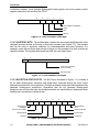


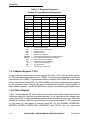
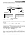


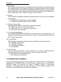
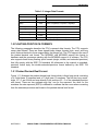


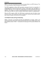
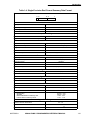


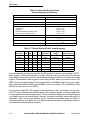


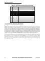


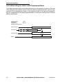
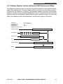


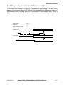
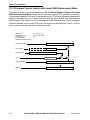


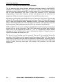
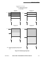


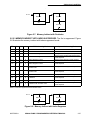


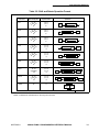


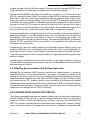


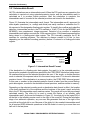

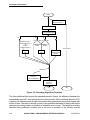


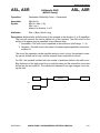

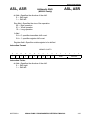
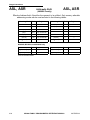


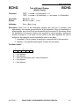


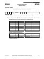
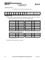
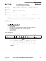
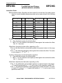


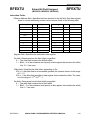

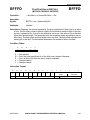
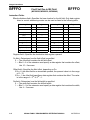
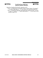


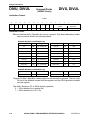

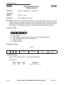
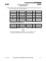


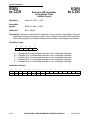


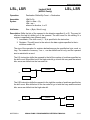


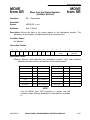


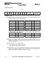


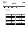


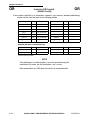
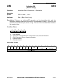


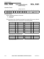
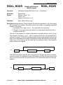


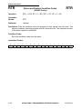

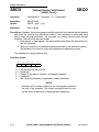


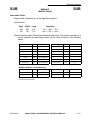


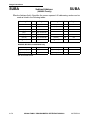

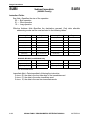


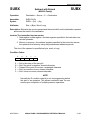


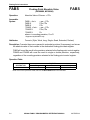


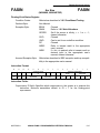

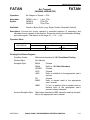

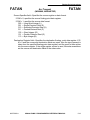

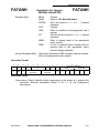


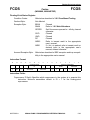


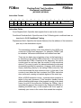


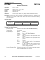


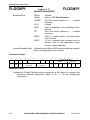
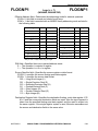

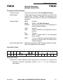
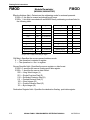
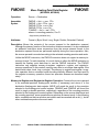

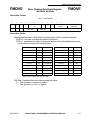

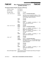
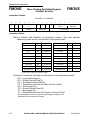

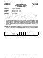


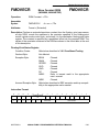


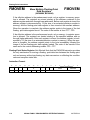


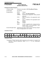


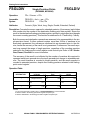
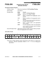


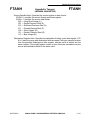


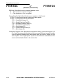


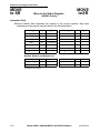

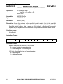


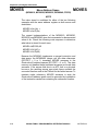

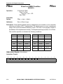


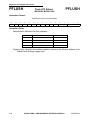


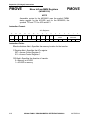
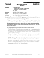
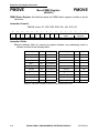

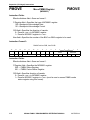


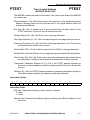

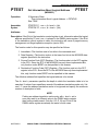
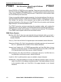

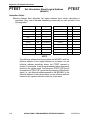

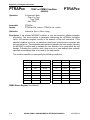

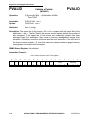

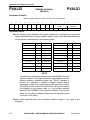


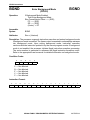

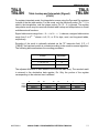


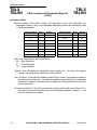


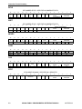
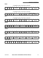
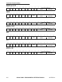
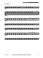


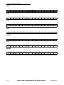

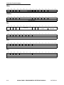


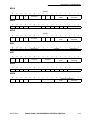

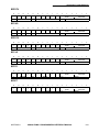

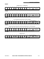


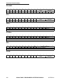

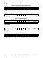
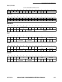


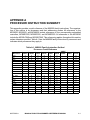
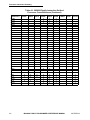


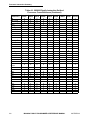


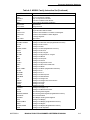


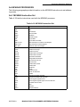

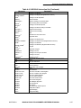
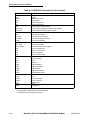
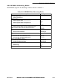
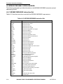


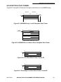


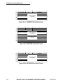


![HiSoft Devpac 3 (text version) [1992] [Manual: PDF]](http://vs1.manualzilla.com/store/data/005668901_1-67cf8256fc448cd2edf58a11a6ec729e-150x150.png)