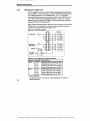
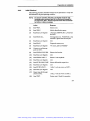
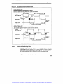
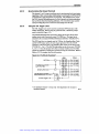
1
Artisan Technology Group is your source for quality
new and certified-used/pre-owned equipment
• FAST SHIPPING AND
DELIVERY
• TENS OF THOUSANDS OF
IN-STOCK ITEMS
• EQUIPMENT DEMOS
• HUNDREDS OF
MANUFACTURERS
SUPPORTED
• LEASING/MONTHLY
RENTALS
• ITAR CERTIFIED
SECURE ASSET SOLUTIONS
SERVICE CENTER REPAIRS
Experienced engineers and technicians on staff
at our full-service, in-house repair center
WE BUY USED EQUIPMENT
Sell your excess, underutilized, and idle used equipment
We also offer credit for buy-backs and trade-ins
www.artisantg.com/WeBuyEquipment
InstraView REMOTE INSPECTION
LOOKING FOR MORE INFORMATION?
Visit us on the web at www.artisantg.com for more
information on price quotations, drivers, technical
specifications, manuals, and documentation
SM
Remotely inspect equipment before purchasing with
our interactive website at www.instraview.com
Contact us: (888) 88-SOURCE | [email protected] | www.artisantg.com
User's Manual
-'"-1
--w
bus
DBS 8750
High-Precision Arbitrary
Waveform Synthesizer
for Precision Signal techno lo^^^
Artisan Technology Group - Quality Instrumentation ... Guaranteed | (888) 88-SOURCE | www.artisantg.com
Proprietary Statement
The information contained in this publication is deriied in part from proprietary and patent data of
the Analogic Corporation. This information has been prepared for the express purpose of
assisting operating and maintenance personnel in the efficient use of the instrument described
herein. Publiiion of this information does not convey any rights to reproduce it or to use it for
any purpose other than in connection with the installation, operation, and maintenance of the
equipment described herein.
P/N 82-51 06
Revision 2
Copyright O Analogic Corporation 1995. All rights reserved.
Printed in U.S.A.
DBS 8701, DBS 8710, and DBS 8750 are trademarks of Analogic Corporation.
Artisan Technology Group - Quality Instrumentation ... Guaranteed | (888) 88-SOURCE | www.artisantg.com
Warranty
Analogic warrants only to the original purchaser that this product, as purchased from Analogic or
an Analogic distributor or dealer, will conform to the written specifications for a period of one year
from the date of purchase. If the product fails to conform to these warranties, Analogic, as its
sole and exclusive liability hereunder, will repair or replace the product and/or its components
within a reasonable periqd of time if the product is returned to a Tektronix service center within
the warranty period. These warranties are made upon the express condition that:
a.
The purchaser promptly notify Tektronix in writing of any non-conformity with the above
warranty including a detailed explanation of the alleged deficiencies.
b.
The product is returned to a Tektronix service center at the buyer's expense after making
suitable arrangements for performance of service.
c.
When the product is returned for repair, a copy of the original bill of sale or invoice is sent
with the product.
d.
Analogic will not be liable for any incidental or consequential damages.
e.
In the opinion of Analogic upon inspection, the product has not been misused, altered, or
damaged due to abnormal handling and/or operation.
f.
Repairs to the product and/or its components have not been made by anyone other than
Analogic or one of its authorized repair agents.
g.
The product has not been modified, altered, or changed in any manner by anyone other than
Analogic or one of its authorized repair agents.
THIS WARRANTY EXCLUDESALL OTHER WARRANTIES, WHETHER EXPRESSED OR
IMPLIED, ORAL OR WRITTEN, INCLUDING WITHOUT LIMITATION WARRANTIES OF
MERCHANTABiUTY AND/OR FITNESS FOR A PARTICULAR PURPOSE.
No term, condition, understanding or agreement purporting to modify the terms of this warranty
shall have any legal effect unless made in writing and signed by an authorized officer of Analogic
and the purchaser.
Iii
Artisan Technology Group - Quality Instrumentation ... Guaranteed | (888) 88-SOURCE | www.artisantg.com
Artisan Technology Group - Quality Instrumentation ... Guaranteed | (888) 88-SOURCE | www.artisantg.com
Contents
1
Introduction
1.1 PRODUCT DESCRIPTION ................................................................
1.1.1 Functional Overview ................................................................
1.1.2 Accessories .............................................................................
1.2 TECHNICAL SUPPORT ....................................................................
Preparation & Installation
2.1 OVERVIEW .......................................................................................
2.2 HARDWARE JUMPERS ....................................................................
2.2.1 Selecting the Base Address ....................................................
2.2.2 Selecting the Address Space ..................................................
2.2.3 Selecting I T L Trigger Lines ....................................................
2.2.4 Deglitching Filter Selection ......................................................
2.3 INSTALLATION .................................................................................
2.3.1 Input/Output Connections ........................................................
2.3.2 Analog Outputs .......................................................................
2.4 START-UP AND VERIFICATION ......................................................
2.4.1 Power-Up Status .....................................................................
2.4.2 Initial Checkout ........................................................................
Operation
3.1 OVERVIEW .......................................................................................
3.2 CONTROLS AND INDICATORS .......................................................
3.3 GENERATING STANDARD WAVEFORMS ......................................
3.3.1 Selecting the Waveshape ........................................................
3.3.2 Selecting the Frequency..........................................................
3.3.3 Selecting the Amplitude ...........................................................
3.3.4 Selecting the DC Offset ...........................................................
3.3.5 Selecting the Drive Mode ........................................................
3.3.6 Selecting Attenuation ..............................................................
3.3.7 Selecting the Filter ..................................................................
Artisan Technology Group - Quality Instrumentation ... Guaranteed | (888) 88-SOURCE | www.artisantg.com
3.3.8 Using Track-and-Hold .............................................................
3.3.8.1 Tracking Mode ...........................................................
3.3.8.2 Track-and-Hold Synchronization ...............................
3.3.8.3 Controlling Track-and-Holdwith
a Front Panel CLOCK ................................................
3.3.9 Using the Deglitching Filter ....................................................
3.3.10Switching the Output Channel State to OnIOff ...........;............
3.3.11 Selecting the GATE Delay .......................................................
3.3.12 Synchronizing the Output Channels ........................................
3.3.13Using the TTL Trigger Lines ....................................................
3.3.14Generating Clean Squarestaircase Waves .............................
3.4 GENERATING ARBITRARY WAVEFORMS .....................................
3.4.1 S0URce:FUNCtion USER Waveforms ...................................
3.4.2 S0URce:FUNCtion MEMory Waveforms ................................
3.5 DSPRJSER MEMORY .......................................................................
3.5.1 Creating Memory Buffers ........................................................
3.5.2 Saving Waveforms ..................................................................
3.5.3 ReadlWrite VXI Memory ..........................................................
3.5.4 Acquiring LOCALbus Data ....................................................
3.5.5 Allocating Memory ...................................................................
3.5.6 Memory Status ........................................................................
3.5.7 Deleting Buffers.......................................................................
3.6 TRIGGERING ....................................................................................
3.6.1 Internal Trigger ........................................................................
3.6.2 External Trigger .......................................................................
3.6.3 Trigger Sequences ..................................................................
3.6.3.1 Programming Guidelines ...........................................
3.6.3.2 Example #1:Complex Wave Burst Internal Trigger ..........................................................
3.6.3.3 Example #2:Sine Wave Burst External Trigger .........................................................
3.6.3.4 Example #3: Free Running Complex Wave ...............
3.7 CLOCK SOURCES ............................................................................
3.8 DIAGNOSTIC TESTS ........................................................................
3.8.1 EPROM Checksum Test .........................................................
3.8.2 SRAM Test ..............................................................................
Artisan Technology Group - Quality Instrumentation ... Guaranteed | (888) 88-SOURCE | www.artisantg.com
3.8.3
3.8.4
3.8.5
3.8.6
4
DAC Output Test .....................................................................
DAC Waveform Memory Test .................................................
Register Test ...........................................................................
Running All Diagnostic Tests ..................................................
DBS 8750 Command Reference
4.1 INTRODUCTION ..............................................................................
4.2 COMMAND SYNTAX ..................... ...............................................
4.2.1 Abbreviated Commands ..........................................................
4.2.2 Command Concatenation........................................................
4.2.3 Command Parameters ............................................................
4.2.4 Optional Keywords and Parameters........................................
4.2.5 Output Channel Selection .......................................................
4.2.6 Query Commands ...................................................................
4.4 DBS8750COMMANDINDEX ..........................................................
..
Appendix A
Specifications
Appendix B
VXI Connections
Appendix C
Error Messages
Appendix D
Revision 0 Hardware
Tables
Hardware Jumper Setup Summary ................................................
Logical Address Setup Examples ..................................................
Address Mode Selections ..............................................................
TTL Trigger Line Output Selections ...............................................
Deglitching Filter Jumper Selections ..............................................
OUT 1 & 2 Default Power-On State ...............................................
Mathematical Mnemonics and Symbols.........................................
Trigger Sequence Control Commands ...........................................
CALC:MATH Command Mnemonics & Symbols ...........................
vli
Artisan Technology Group - Quality Instrumentation ... Guaranteed | (888) 88-SOURCE | www.artisantg.com
Figures
3-10
3-11
3-12
3-13
3-14
3-15
3-16
3-17
3-18
3-19
3-20
3-21
4-1
4-2
6-1
0-2
Waveform Synthesizer Block Diagram...........................................
DBS 8750 Jumper Selection Locations..........................................
TTLTRG Interface ..........................................................................
Output Channel Connectors 1 & 2 .................................................
DBS 8750 Command Set Quick Reference ...................................
DBS 8750 Front Panel ...................................................................
Simplified Output Stage Schematic ...............................................
Output Voltage Characteristics ......................................................
Output vs. Tracking Mode ..............................................................
Synchronizing the Track/Hold ........................................................
Track/Hold Control for Sine Function .............................................
TRIG-GATE Timing .......................................................................
lTLTRG I10 Functions...................................................................
Square Wave Generation with InternalIExternal Clock .................
Complex Waveform By Segments .................................................
1-kHz Sine Wave Output ...............................................................
Log Function Output ......................................................................
Exponential Output Waveform .......................................................
Rectification Using Absolute Function ...........................................
DSPIUser Memory Example ..........................................................
LOCALbus Timing Diagram ...........................................................
Example #1 Output Wave ..............................................................
Example #2 Output Wave ..............................................................
Example #3 Output Wave ..............................................................
Front Panel CLOCK Input Circuit ...................................................
DBS 8750 Command Tree .............................................................
Comcatenating Commands ...........................................................
Connector P I .................................................................................
Connector P2 .................................................................................
Artisan Technology Group - Quality Instrumentation ... Guaranteed | (888) 88-SOURCE | www.artisantg.com
Section I
Introduction
1.1
PRODUCT DESCRIPTION
The DBS 8750 is a 400 kHz, 16-bit precision, VXI Message-Based Arbitrary Waveform Synthesizer. Using its command set, the DBS 8750 can
generate highly-accurate standard and arbitrary waveforms on either of its
two differential or single-ended output channels. Combining the superior
performance of a dual digital-to-analog converter (DAC) with the speed and
processing capability of a digital signal processor (DSP), the DBS 8750
provides precision analog output signals.
Functional Overview
The DBS 8750 (Figure 1-1)generates waveforms using the data placed in
the DAC 1or 2 Waveform Memory (32K words maximum per channel).
The DAC Sampling Rate is controlled by either the 400-kHzInternal
Sampling Rate Clock or an External Sampling Rate Clock received from the
Front Panel CLOCK input or one of the TTL Trigger lines via the VXIbus.
The waveform data can be obtained from any of the following sources:
(1) Standard Waveform Library - Sine, Square, Triangle, Noise and DC
functions.
(2) User-Defined Waveform Function - Complex waveforms calculated by
the DSP according to a prescribed formula and user-specified parameters. Maximum waveform size is 32K points.
(3) DSP/User Memory. The shared DSPIUser memory has 17150 words of
user-accessible readlwrite space for saving waveforms and acquiring
waveform data from the VXI system.
All control functions, complex waveform calculations and digital signal
processing are implemented by the DSP. The DSP serves as an intelligent
DMA controller for transferring digital data between the VXIbus and the
DSP/User Memory. The DSP also acts as a counterltiming sequencer for
cross-synchronization with other VXI instruments.
Artisan Technology Group - Quality Instrumentation ... Guaranteed | (888) 88-SOURCE | www.artisantg.com
DBS 8750 User's Manual
Figure 1-1. Waveform Synthesizer Block Diagram
I
On the front panel, an External Trigger input, an External Clock input and a
Gate output provide synchronization controls. T o cross-synchronize its
operation with another VXI instrument, such as a DBS 8700 Digitizer, the
DBS 8750 uses the VXlbus l T L Trigger lines to provide a Sampling Rate
Clock and/or GATE output, or to receive an External Sampling Rate Clock.
NOTE:
The DAC Waveform Memories are not accessible from the
Wlbus. The shared DSPNser Memory has 17150 words of
user-acccessible readlwrite space for data transfers to/from
VXI memory or from the LOCALbus via connector P2.
After data has been loaded or processed, the DSP writes the final values into
the DAC 1or 2 Waveform Memory. In the write mode the memory is
addressed by the DSP,while in the read mode the memory is addressed by a
set of address counters. In turn, each DAC memory has its own independent
address counter which allows independent waveform generation at each of
the two outputs. While operating from pre-loaded commands and after the
address counter has reached its last address, the channel loops back and
continues to output the same waveform until a new command is entered at
which time generation of a new waveform begins.
Artisan Technology Group - Quality Instrumentation ... Guaranteed | (888) 88-SOURCE | www.artisantg.com
-
Introduction
The analog output section is isolated from the digital section of the card by a
500-volt dc barrier. High-speed pulse transformers couple the data and
control signals across the barrier. As each waveform memory outputs 16-bit
parallel data words, a parallel-to-serial shift register feeds a serial bit stream
over the barrier, while on the floating side, a serial-to-parallel shift register
reverses the process. To maintain proper DAC synchronization, the 16-MHz
master clock as well as the track-and-hold and load control signals are
passed across the barrier using separate transformers.
Under precision timing control, digital data from each DAC memory is
converted to analog signals by a highly-accurate I s b i t dual DAC. Each
DAC converts data at the sampling rate and provides its own stable reference and two distortion-suppressing output deglitcher amplifiers.
Each DAC output is fed into a 6-pole reconstruction low-pass filter which
can be switched into the analog path to eliminate higher frequencies when
harmonically clean signals are required. A programmable attenuator feeds
the filtered signal to the output amplifier. The output amplifier can be
configured for either a single-ended or differential output, with AC or DC
coupling, and with 50 or 600 ohms of output impedance. When finer
attenuation steps are required, sending the appropriate commands to the DSP
produces digitally scaled data within the full 16-bit resolution of the DACs.
A very low noise DC-to-DC converter designed to accommodate the
stringent demands of a highly-accurate 16-bit waveform synthesizer
provides power to the isolated analog section. Powered by +5 volts from
connectors PI and P2, the DC-to-DC converter provides regulated and
filtered +IS, -15 and +5 volts for the entire analog output circuitry.
1.1.2
Accessorles
Q DVX05-3
3-foot cable/connector assembly
DVX05-5
5-foot cable/connector assembly
These assemblies consist of a TWBNC connector attached to either a %foot
or 5-foot length of twisted shielded-pair cable. The other end of the cable
has two cable conductors and a shield available for direct connection to the
user's hardware application.
TECHNICAL SUPPORT
For service, contact your nearest Tektronix Service Center.
For technical support, call 1-800-835-4894 for technical support in the U.S.,
or contact your nearest Tektronix Office outside the US.
Artisan Technology Group - Quality Instrumentation ... Guaranteed | (888) 88-SOURCE | www.artisantg.com
DBS 8750 User's Manual
Artisan Technology Group - Quality Instrumentation ... Guaranteed | (888) 88-SOURCE | www.artisantg.com
Section 2
Preparation & Installation
OVERVIEW
This section provides instructions for setting up hardware jumpers and
installing the instrument in a VXI chassis. After unpacking, carefully
inspect the hardware for any damage that may have occurred during shipment. If necessary, contact the carrier to file a claim. Save the shipping
carton and packing materials if for any reason you need to return the product
for repair or replacement. For technical support or to return this product to
the factory, refer to Section 1.2 for instructions.
CAUTION:
This product contains components which are sensitive t o
electrostatic discharge (ESD). Be s u r e t o follow proper
procedures for handling, storing and transporting ESDsensitive assemblies.
HARD WARE JUMPERS
Before installing this instrument in a chassis, check Table 2-1 which lists
jumper
selections made at the factory before shipment To change any
.
factory selection, refer to Figure 2-1 and the referenced Section.
-
Table 2-1. Hardware Jumper Factor Setup
Factory
S e c t Selection
Function
VXI Logical Address
Address Space
Sampling Rate Clock Output
Deglitching Filter
A24
mmGO
In tine
Factory Setup Only
For hardware revision 1 and up only. See Appendix D for revision 0
hardware jumpers.
2-1
Artisan Technology Group - Quality Instrumentation ... Guaranteed | (888) 88-SOURCE | www.artisantg.com
-.-
DBS 8750 User's Manual
Figure 2-1. DBS 8750 Jumper Selection Locations*
A241A32
Address
Mode
Base
Address
----.
u;;
:Factory j
US9 JP12 $
: Only.
:
2;
JPll
4
j Factory
--
<&Use Only.
i
i
,
Deglitching
Filter Bypass
.
'
F1
SP005
Power
Input
Fuse
JP21 JPP
NOTE:
Jumpers JP9 and J P l l - JP18 are used only at the factory.
They are Installed at the factory In the following arrangement
and should not be altered: JP9 and JP11 are always jumpered
2-3; JP12 and JP13 JP18 are always open.
-
For hardware revision 1 and up only. See Appendix D for revision 0
hardware jumpers.
Artisan Technology Group - Quality Instrumentation ... Guaranteed | (888) 88-SOURCE | www.artisantg.com
Pre~aration& Installation
22.1
Selecting the Base Address
The Base address of a VXI instrument is determined by the following:
Base Address = (Logical Address x 64) + 49152
The Logical Address of this instrument can be set from 0 to 255d using
jumpers JP1 through JP8. However, Logical Address 0 and 1 cannot be
used as these addresses are used by various VXI embedded controllers.
Table 2-2 list some examples.
NOTE:
Do not use Logical Address 0 or 1. These are reserved for
system controllers.
Table 2-2. Logical Adddress Setup Examples
VXlbus Address Lines & Jumper Selections
VAl3 VA12 "A11 VA10 VAO VA8
VA7
VA6
Addresr
'
255
254
252
248
240
224
192
132
2
2.2.2
Selecting the Address Space
The setting of hardware jumper JPlO enables the instrument to operate in
either the A24 or A32 addressing mode. Refer to Table 2-3.
Table 2-3. Address Mode Selections
Artisan Technology Group - Quality Instrumentation ... Guaranteed | (888) 88-SOURCE | www.artisantg.com
DBS 8750 User's Manual
2.2.3
selecting 77L Trigger Lines
The TTL trigger lines can be used for additional triggering and synchronization capabilities. As shown in Figure 2-2, the selected Sampling Rate Clock
can be jumper-selected to drive TTLTRG line O,1,2 or 3. The GATE
output from the front panel can be jumper-selected to drive TTLTRG 4,5,6
or 7. Table 2-4 lists the available jumper selections. Before one of these
signals can drive the bus, the TTLTRG line drivers must first be enabled by
command 0UTPut:'ITLTrg ON IOFF.
Also, an External Sampling Rate Clock input can be received on any unused
TTLTRG line. The input clock is software selected using the command,
S0URce:ROSCillator:SOURcelTLTRG <0-7>.
Figure 2-2. TTLTRG interface'
JP20
VXlbus
Table 2-4. TTL Trigger Une Output Selectionst
J u I ~ DI setting
~ ~
I connection
I
JP19
l to4 I
1 to P
5 to 6
JP20
Sampling Rate Clock onto ITLTRGP
1 7 to 8
1 1 to 2
1 Sampling Rate Clock onto lTLTRG3
1 GATE output pulse onto lTLTRG4
3 to 4
GATE output pulse onto lTLTRG5
GATE output pulse onto lTLTRG6
GATE output pulse onto TTLTRG7
5 to 6
7 to 8
I
Sampling Rate Clock onto lTLTRGO
Sampling Rate Clock onto lTLTRGl
* Factory Selection
f
For hardware revision 1 and up only. See Appendix D for revision 0
hardware jumpers.
Artisan Technology Group - Quality Instrumentation ... Guaranteed | (888) 88-SOURCE | www.artisantg.com
Preparation & Installation
2.2.4
Deglitching Filter Selection*
Each channel of the dual D/A Converter (DAC) is fed to a deglitching filter
network where the filter can be connected in line with the DAC output or
bypassed (Table 2-5). Bypassing the filter provides improved DC performance. For more information, refer to Section 3.3.9
Table 2-5. Deglitching
- Filter Jumper Selections
Selection
In Line
Bypassed
2.3
Channel 1
JP21-2 to JP21-3
JP21-1 to JP21-2
Channel 2
JP22-2 to JP22-3
JP22-1 to JP22-2
Application
Sine, Triangle
Square, Pulse, Step
Functions, DC
INSTALLATION
The 8750 can be installed in any slot except slot 0. Any module used in
synchronous operation with the 8750 via the LOCALbus on connector P2
must be installed in the adjacent slot to the right of the 8750.
2.3.1
Input/Output Control Connections
The front panel controls and indicators are described in detail in Section 3.
However, for installation purposes, the characteristics of the inputloutput
connections are provided here.
CLOCK External clock input (BNC, 50Q) - accepts a 'ITL, negative-going
pulse (120 ns, min.), maximum frequency of 400 kHz.
2.3.2
TRIG
External trigger input (BNC, 50Q) - accepts a TTL, active-low
signal to allow waveform generation.
GATE
Gate output (BNC) - a lTL, active-low output during waveform
generation, synchronized with the Internal Sampling Rate Clock.
Analog Outputs
The analog outputs OUT 1and OUT 2 (Figure 2-2) are provided o n
TWBNC connectors. The outputs are switch selectable for 50 or 600 ohms
output impedance and AC/DC coupling. The output stage is software
selectable for a single-ended or differential configuration.
CAUTION:
The output driver current should not exceed 40 mA, max.
For hardware revision 1 and up only.
Artisan Technology Group - Quality Instrumentation ... Guaranteed | (888) 88-SOURCE | www.artisantg.com
DBS 8750 User's Manual
Figure 2-3.
Output Channel Connectors 1 & 2
Pin...........Signal +
Socket.....Signal -
Shell........Signal Ground
(Isolated)
Output Impedance
Selection Switch
Acme CouNinp
Selection Switch
2.4
START-UP AND VERIFICATION
2.4.1
Power-Up Status
At power-on, a self-test is executed. The Pass/Fail indicator is red during
the test (4.8 seconds) and switches to green when the test passes (see *TST?
command in Section 4). Both output channels assume the default parameters listed in Table 2-6 following the self-test.
Table 2 8 . OUT 1 & 2 Default Power-On State
Function
State
Output Filters
Attenuation
Output Drive
On/Off State
Waveshape
Frequency
Voltage
Offset Voltage
Memory Buffers
Oscillator Source
Trigger Source
Trigger Sequence Count
Tfgger Loop Count
Bypassed
0.00 dB
Differential
OFF
DC
1000.00 Hz
0.00 v
0.00 v
None defined
Internal
Internal
0
0
Artisan Technology Group - Quality Instrumentation ... Guaranteed | (888) 88-SOURCE | www.artisantg.com
Preparation & Installation
2.4.2
Initial Checkout
The following procedure describes tests that can be performed to verify that
the instrument is in good operating condition.
NOTE:
For proper operation, the Data Low Register must be read
following every command sent to this instrument except for
the command, %ST. Normal response is the new llne character (xOA) or a status message.
Action
Response
Send *RST.
System reset.
Send *IDN?
Module identification query.
Read Data Low Register
"Analogic, DBS8750, Rev n, Firmware
Revision"
Send D1AG:ALL.
All diagnostics run. PASS/FAIL is red,
switches to green after all tests pass.
Read Data Low Register
xOA
Send DIAG?
Diagnostic status query.
Read Data Low Register
"No errors, self test PASSED"
Connect an oscilloscope
probe to OUT1.
Send SOUR1:FUNC SIN.
Selects sine function.
Read Data Low Register.
xOA
Send SOUR1:VOLT 5
Selects 5-volt amplitude.
Read Data Low Register.
xOA
Send OUTP1:DRIV DIFF. Selects differential output drive.
Read Data Low Register.
xOA
Send OUTP1:STAT 1.
1-kHz, 5-volt sine wave on OUT 1.
Read Data Low Register.
xOA
Repeat steps (8) through
(16) for OUT2
1-kHz, 5-volt sine wave on OUT 2.
Send *RST.
System reset. Ready for operation.
Artisan Technology Group - Quality Instrumentation ... Guaranteed | (888) 88-SOURCE | www.artisantg.com
DBS 8750 User's Manual
Artisan Technology Group - Quality Instrumentation ... Guaranteed | (888) 88-SOURCE | www.artisantg.com
Section 3
Operation
3.1
OVERVIEW
This section describes how to operate the DBS 8750 using the DBS 8750
Command Set (Figure 3-1). This command set is used to control the
generation of standard and arbitrary waveforms, data transfers to and from
memory, triggering, clock selection and diagnostic tests. See Section 4, the
DBS 8750 Command Reference, for more information.
NOTES: When programming this instrument it is necessary to read the
Data Low Reglster after sending every command except Reset,
*RST. The normal response Is the new llne character (xOA) or
a status message.
The DAC Waveform Memorles are not accessible from the
VXlbus. The shared DSPNser Memory has 17150 words of
user-acccesslble readlwrite space for data transfers toffrom
VXi memory or from the LOCALbus via connector P2.
If this instrument is to be controlled using a software driver,
refer to the Software User's Manual received with the driver for
software installation and operating instructions.
Error messages are generated for operational errors that are
related to command entry, execution, triggering, data entry, or
memory usage. See Appendix C for a list of possible error
messages.
CONTROLS AND INDICATORS
Figure 3-2 describes the control inputs and indicators on the front panel.
After making jumper selections and installing the instrument, all inputs and
outputs are operated by software commands. Note that input coupling and
input impedance are selected using front panel switches rather than using
software commands.
Artisan Technology Group - Quality Instrumentation ... Guaranteed | (888) 88-SOURCE | www.artisantg.com
DBS 8750 User's Manual
lgure 3-1. DBS 8750 Command Set Quick Reference
....-.CALCulate
:MATH <Segment 1> <Segment 2> <Segment 3> ...... <Segment 16>
NAGnostk Subsystem ......DlAGnostic
:ALCulato Subsystem
:EPRom
:SRAM
ANAL*
:DRAM
:REGS
:AlL
...........MEMory
MEMory Subsystem
:WRITe<sp>cVXI Addh<sp><Npts><sp><Buffer Name>
:READcsp><VXI Addrxsp>cNpts>csp><Buffer Name>
:SAV1(2)<sp><Buffer Name>
ACQuiecsp><Npts>csp>cBuffer Name>
:CATalog[:ALL]? I BINary?
:DELete<sp><Buffer Name> I ALL
:FREE[:ALL]? I BINary?
:MALLocate<sp>cBuffer Namexsp>cNpts>
OUTPut Subsystem
............OUTPut(lI(2)
:ATTenuationcsp><O to 90>
:FILTer<sp>ON 1 OFF
:STATe<sp>ON IOFF
:DRIVe<sp>SINGle-ended I DlFFerentii
:TRACkcsp>ON I OFF
:GAT
:DELay<sprc0.00002 to 41.945
:SYNC
lTLTrgcsp>ON I OFF
SOUR-
Subsystem
...........SOURce[l](2)
:FREQuency<sp><l2.5 to 20000>
:VOLTagecsp>c-10 to +lo>
:OFFSet<sp><-10 to +lo>
:FUNCtiicsp>DC I SlNe ( SQUare I TRlangle ( NOISe I USER ) MEMor)
:ROsciilator
:SOURce<sp>lNT I UCT I TTLTrgcO-7>
:AUTO SHON I SHOF
TRlGger Subsystem
...........TFlIGger[l](2)
:SEQuence[l](2)
:STAR
:STOP
:COUNtcsp>cnumeric~
:COUNt<sp><numeric>
:SOURcecsp>EXT I INT
Artisan Technology Group - Quality Instrumentation ... Guaranteed | (888) 88-SOURCE | www.artisantg.com
Operation
Figure 3-2. DBS 8750 Front Panel
External Clock Input (BNC)
Accepts a I T L level, adwe low dock; maximum frequency
of 400kHz and pulse width of 120 ns (rnin.).
ExternalTrigger Input (BNC)
Accepts a 'Tn, active low input signal which allows
waveform generation during the low period.
mm
Gate Enable Output (BNC)
m,
Produces a
active low output signal during waveform
generation, synchronized with the Internal Precision Clock.
Can be programmed for a delay of 20 ps to 41.94seconds.
instrument Reset Pushbutton
Resets the DSP, swlches both outputs off, executes the
power-up self-test diagnostic and leaves the instrument in
the power-up default state.
PassIFall indicator
Indicates diagnostic test results: Pass = Green, Fail = Red.
Channel 1 Output (IWBNC)
Channel 1 analog output. Pin is (+), Socket is (-).
Programmable differential or single-ended output drive.
OUT 1 lmpedance Switch
[glL
Sets channel 1 output impedance to 50 or 600 ohms.
OUT 1 Coupling Switch
Sets channel 1 output coupling to AC or DC.
-n
1
1
Channel 2 Output (TWBNC)
Channel 2 analog output. Pin is (+), Socket is (-).
Programmable differential or single-ended output drive.
OUT 2 lmpedance Switch
Sets channel 2 output impedance to 50 or 600 ohms.
\- OUT 2 coupling switch
Sets channel 2 output coupling to AC or DC.
3.3
GENERATING STANDARD WAVEFORMS
The commands used to generate standard waveforms are found in the
SOURce and OUTput subsystems o f the DBS 8750 Command Tree.
Although the commands that determine waveform characteristics may be
written i n any order, i t is recommended that all characteristics be setup
before changing the state o f the output to ON.
Artisan Technology Group - Quality Instrumentation ... Guaranteed | (888) 88-SOURCE | www.artisantg.com
DBS 8750 User's Manual
.
NOTE: The filter should be ON when generating waveforms. If W Is
OFF and the internal clock is used to generate square or
triangle waves, the acurracy is limited due to spikes introduced from the Track and Hold control circuit (Section 3.3.8).
3.3.1
Selecting the Waveshape
Standard waveshapes are set up by sending the following command:
SOURce[l](2):FUNCtion DC 1 SINe I SQUare I TRIangle I NOISe
DC ..... ...............DC output level
SINe ...................Sine wave
SQUare .............. Square wave
TRIangle ............Triangle wave
NOISe ................Random noise
After all other parameters are set up (frequency, amplitude, DC offset, etc.),
the selected output function appears at the output connector when the output
channel is switched on by sending OUTPut[l](2):STATe ON.
3.3.2
Selecting the Frequency
The output signal frequency is set up by sending the following command
(does not apply to DC and NOISe functions):
where n = 12.5 to 20000 Hz for the Sine function,
12.5 to 30000 Hz for the Square and Triangle functions.
3.3.3
Selecting the Amplitude
The output amplitude is set up by sending the following command:
SOURce[l](2):VOLTage n,
where n = +10.000 to -10.000 volts for a single-ended output drive;
+5.000 to -5.000 volts for a differential output drive.
The numeric value "nurepresents peak voltage. To prevent clipping,
amplitude plus offset should not exceed full scale.
3.3.4
Selecting the DC Offset
The dc output offset is set up by sending the following command:
SOURce[l](2):VOLTage:OFFset n
where n = -10.000 to + 10.000 volts
Artisan Technology Group - Quality Instrumentation ... Guaranteed | (888) 88-SOURCE | www.artisantg.com
Operation
3.3.5
Selecting the Drive Mode
Each channel can be configured for single-ended or differential output drive
mode. Figure 3-3 shows a simplified schematic of the output stage. The
output coupling and impedance switches are located on the front panel. As
you can see, the output drive can be configured for a single-ended or
differential output drive depending upon the state of the relay switches. To
program the output drive, send the following command:
OUTPut[l](2):DRIVe SINGle-ended I DIFFerential
SINGle-ended .... Single-ended output drive
DIFFerential ...... Differential output drive
NOTE:
The Slngle-Ended output drive has a range of 20 (do) volts.
The Differential output drive has a range of 10 (6)
volts.
Maximum output current should not exceed 40 mA.
As shown in Figure 3-4, the actual programmed peak voltage amplitude and
voltage offset value are produced at the output connector under open circuit
conditions only. When a load is connected, the programmed voltage values
are reduced. The amount of reduction depends upon the output impedance
of the DBS 8750 and the input impedance of the load. As you can see,
applying a load to the output creates a voltage divider with the series output
resistance (50 or 600 ohms) of the instrument. The actual voltage level
measured at the output depends upon the ratio of the input and output
impedances.
flgure 3-3. Simplified Output Stage Schematic
Output Signal from
Attenuator Circuits
Front Panel Switches
Coupling
Impedance
Output State
Output ON, SE
Output ON, DlFF
Relay A Relay B
On
Off
On
On
Artisan Technology Group - Quality Instrumentation ... Guaranteed | (888) 88-SOURCE | www.artisantg.com
DBS 8750 User's Manual
Figure 3-4. Output Voltage Characteristics
Output with 509hm Load
Open Circuit Output
t
V
'
3.3.6
Example Set-Up:
Function = Sine Wave
Amplitude = 2 V (peak)
Offset=+l v
Impedance = 50
Selecting Attenuation
The output signal can be attenuated from 0 to 90dB by sending,
OUTPut[l](2):AlTenuation n, where n = 0 to 90
Output attenuation is accomplished by a combination of a switched resistor
network and voltage reduction performed by mathematical calculation. The
resistor network provides attenuation steps of OdB, IOdB, 20dB and 30dB.
Other settings are completed by mathematical calculations which lower the
output voltage an additional amount.
3.3.7
Selecting the Filter
An output reconstruction filter is available for low-distortion sine wave
generation. The filter is connected in line or bypassed by sending the
following command:
OUTPut[l](2):FILTer
O N or 1 ( OFF or 0
ON or 1 ..............to connect the filter
OFF or 0 ............to bypass the filter
Normally, the filter should be switched ON. However, the instrument may
be used
- - . -with the filter switched OFF for certain step functions. Always
-
~
-
--
-~
switch the filter ON to generate low distortion SINe waves. See also Section
3.3.8 for use of Track-and-Hold with SINe waves.
Artisan Technology Group - Quality Instrumentation ... Guaranteed | (888) 88-SOURCE | www.artisantg.com
3.3.8
Using Track-and-Hold
3.3.8.1
Tracking Mode
The Tracking Mode is selected by using the following command:
OUTput[l](2):TRACk ON or 1I OFF or 0
ON or 1 .............. Track Only
OFF or 0 ............Track and Hold
Figure 3-5 shows the affects of the Tracking Modes on the Digital-toAnalog @AC) output signal. When generating sine waves, always switch to
the Track-and-Hold Mode which reduces the code-dependent glitch energy
on the DAC output. For DC levels, switch to the Track Only Mode to
prevent ~ r a c k ~ oswitching
ld
noise on the DAC output. he Track Only
Mode is also useful for reducing square wave settling times. However,
glitch energy at major DAC code transitions will be higher.
-
Figure 3-5.Output vs. Tracking
- Mode
Track & Hold Mode
0UTPut:TRACk OFF
DAC Digital
Input
rackh hi old Switching ~ o i s e
DAc output
,
I
j
! '
I
I
1
I
1
I
I
I
Track Only Mode
0UTPut:TRACk ON
DAC Digital
Input
Track always tnie.
I
I
code-Dependent Flitches
I/
DAC Output
Changing
Code
+v
..
1' I
I
I
I
I
I
I
I
I
I
I
I
I
,,
----------.-----------------
DAC Outwt
~nchanghg
Code
Artisan Technology Group - Quality Instrumentation ... Guaranteed | (888) 88-SOURCE | www.artisantg.com
DBS 8750 User's Manual
3.3.8.2
Track-and-Hold Synchronization
The Track-and-Hold Mode can be synchronized with either the 400-kHz
Internal Sampling Rate Clock or an External Sampling Rate Clock via the
front panel CLOCK input (Figure 3-6). To synchronize the Track-and-Hold,
use the following command:
SOURce:ROSCillator:SOURce:AUTOSHON I SHOF
SHON
...Synchronize Track-and-Hold with Front Panel CLOCK input.
SHOF .... Synchronize Track-and-Hold with Internal Sampling Rate
Clock (Default).
Flgure 3.6. SynchronWng the TracWHold
SHON 1 SHOF
OUTPUT
FILTER
Front Panel CLOCK
Internal Sampling-)O
.
Rate Clock
SHOF
. - - - - - - - 0UTP:TRAC ON
1 OFF
3.3.8.3 Controlling Track-and-Hold with a Front Panel CLOCK
An External Sampling Rate Clock connected to the Front Panel CLOCK
input (not the 'ITLTRG lines) can be used to control the DAC Track-andHold Output Amplifiers (Figure 3-7). This feature is especially useful for
generating low-distortion Sine waves. For this purpose, the CLOCK input
should be a 350 to 400-kHz, negative-going pulse with a pulse width of
1 . 2 ~ *Sons,
s
and less than 100 pS of jitter. Refer to Section 3.7 for infonnation on selecting clock sources.
Figure 3-7 shows the affect of clock synchronization on the Track-and-Hold
control. In the top half of the diagram, Track-and-Hold is synchronized with
the External Sampling Rate Clock from the Front Panel. The bottom half
shows synchronization with the Internal Sampling Rate Clock. This
diagram clearly shows that low-distortion sine waves can be generated while
Track-and-Hold is synchronized with an External Sampling Rate Clock
because there is less jitter on the Track-and-Hold control signal.
Artisan Technology Group - Quality Instrumentation ... Guaranteed | (888) 88-SOURCE | www.artisantg.com
-
--
Operation
Figure 3-7.TrackMold Control for Sine Function
0UTPut:TRACk OFF
S0URce:ROSClllator:SOURce:AUTO SHON
Eliminates jitter in Sampling Rate Clock; yields low distortion.
I
1
CLOCK
350 to 400 kHz
50 n s .
TracWHold
output Level
:
-
Track
:
/
:
DAC HOM Level
;
:
0UTPut:TRACk OFF
S0URce:ROSCillator:SOURce:AUTO SHOF
Jier on both edges of TracWHold; yields harmonic distortion.
1-
CLOCK
xio to m k H z 1
TracMiold
Output Level
I
3.3.9
-
:
1-
DAC HOM Level
*Jitter caused by asynchronicity between internal and external clocks.
Using the Deglitching Filter
By jumper selection, the output signal of each DAC may be passed through
a hdglikhing filter (see section 2.2.4) to reduce the affect of noise and glitch
energy on the output. Bypassing the deglitching filter* provides improved
DC output performance and a reduction in square wave settling time.
*
For hardware revision 1 and up only.
Artisan Technology Group - Quality Instrumentation ... Guaranteed | (888) 88-SOURCE | www.artisantg.com
DBS 8750 User's Manual
3.3.10
Switching the Output Channel State to O m f f
As shown previously in Figure 3-3, each of the two analog output channels
can be connected or disconnected independently with a relay switch. These
relays are switched on/off by sending the following command:
OUTPut[1](2):STATe ON or 1 I OFF or 0
ON or 1
..............Connects the output
OFF or 0
............Disconnects the output
The ON state closes a relay to connect the output amplifier to the front panel
OUT l(2) connector. The OFF state opens the relay and switches the
connector output pin to ground through 50 or 600 ohms. During waveform
calculations and initialization, you may wish to keep the outputs OFF, and
only switch them ON after all other parameters have been specified.
3.3.11
Selecting the GATE Delay
The front panel GATE output produces a 'ITL, active-low output signal,
synchronized with the Sampling Rate Clock, during waveform generation.
The GATE output can be programmed for an output delay of 20 p to
41.945 seconds in 2.5-p increments (Figure 3-8). This output can be used
as an external trigger or start signal for another VXI instrument such as a
DBS 8700 Digitizer. By jumper selection (Section 2.2.3), this output can be
made available on ?TL trigger line 4,5,6, or 7 (Section 3.3.13)*. To
program the GATE delay, send the following command:
0UTput:GAT:DELay n, where n = 0.00002 to 41.945 secs in 2 . 5 - p steps
Figure 3-8. TRIG-GATE Timing
I
I
I
I
I
GATE follows I
TRIG high.
I
I
I
GATE
1
I
I
TRIG
I
I
-
GATE Delay
20~s-41.945SeC.
1
* For hardware revision 1 and up only.
I
See Appendix D for revision 0
hardware jumpers.
Artisan Technology Group - Quality Instrumentation ... Guaranteed | (888) 88-SOURCE | www.artisantg.com
Operation
3.3.12
Synchronizing the Output Channels
The channel 1 and 2 output waveforms can be synchronized with each other,
regardless of their current phase relationship, by sending the 0UTPut:SYNC
command (the [1](2) designation not required). This simultaneously resets
the DAC memory address generator for both channels and starts generating
the waveforms from their starting addresses. The waveforms stay synchronized providing they have a harmonic relationship from the start.
3.3.13
Using the TTL Trigger Lines
The TTL Trigger Lines can be used to synchronize 8750 operation with
another instrument. Before using any particular line, a hardware jumper
must be installed (Figure 3-9).
An External Sampling Rate Clock that is being driven onto the bus from
another source can be received on any TTLTRG line. The input line is
selected by the command SOURce:ROSCillator:SOURce TTLTRGeO-7>.
The 8750 can drive two signals onto the VXIbus: the Sampling Rate Clock
and the GATE output pulse, the same signal generated from the GATE
connector on the front panel. The Sampling Rate Clock can be driven onto
TTLTRG O,1,2 or 3. The GATE output pulse can be driven onto lTLTRG
4, 5,6 or 7. Once the jumpers have been correctly installed, the TTLTRG
signals are enabled by sending the 0UTPut:TTLTrg ON command. Refer to
Section 2.2.3 for jumper selection information.
flaure 3-9. lTLTRG I10 Functions*
-VXlbus
----
JWO
TTLTRG Output Enable
0UTP:TTLTON
Sampling Rate Clock
TLTRG Trigger In
---law
-
--
* For hardware revision 1 and up only. See Appendix D for revision 0
hardware jumpers.
3-11
Artisan Technology Group - Quality Instrumentation ... Guaranteed | (888) 88-SOURCE | www.artisantg.com
DBS 8750 User's Manual
63.14
Generating Clean Square/Stalrcase Waves
When generating standard square waves using the 400-kHz Internal Sampling Rate Clock, clock-related noise is evident on the output wave whenever the data point values stay the same across multiple clock edges (Figure
3-10a). This happens because the internal Track-and-Hold circuit of the
DAC is switched at every rising clock edge.
One solution to this problem is to switch the Track-and-Hold mode to
"Track Only" but this creates a different set of problems. The recommended
technique is to bse an External Sampling Rate Clock and create the square
wave so that each different data point value corresponds with a single rising
clock edge (Figure 3-lob). The secret to this technique is to remember that
the 8750 always calculates waveforms based on a 400 kHz sampling rate. If
you want a square wave to change state on every rising clock edge, you must
select a frequency of 200 kHz. This forces the 8750 to create a data pattern
consisting of exactly two data points. Now, if a 20 kHz external clock is
applied, for example, the output waveform is a 10-kHz square wave (half the
external sampling rate) with clock-related noise spikes appearing only at the
rising edges of the external clock.
This same technique applies to other DC-accurate applications such as for
generating staircase (Figure 3-10c) or pulse waveforms.
Artisan Technology Group - Quality Instrumentation ... Guaranteed | (888) 88-SOURCE | www.artisantg.com
Operation
Flgure 3-10. Square Wave Generation with InternalIExternal Clock
400 kHz Internal Clock
Output Square Wave
Output noise spikes synchronous with Sampling Rate Clock.
a.
External Sampling Rate Clock
Output Square Wave
edges.
Clock edges corresponding with 'data' edges.
b.
External Sampling Rate Clock
output Staircase Wave
llnn-r
L
Staircase Waveform Generation
c.
Artisan Technology Group - Quality Instrumentation ... Guaranteed | (888) 88-SOURCE | www.artisantg.com
DBS 8750 User's Manual
3.4
GENERATING ARBITRARY WAVEFORMS
Arbitrary waveforms can be generated by either of the two commands
SOURce[l](2):FUNCtion USER or SOURce[l](2):FUNCtion MEMory.
3.4.1
S0URce:FUNCtion USER Waveforms
The USER function generates waveforms which have been calculated by the
CALCulate[l](2):MATH command. USERdefined waveforms may consist
of up to 16 user-defined segments, but the total waveform length must be no
more than 32K-words (Refer to Section 3.5 on memory and waveform size).
The format of the CALCulate[l](2):MATH command is as follows:
where <segment n> = FORcsp><duration><sp><voltage>,
a mathematical expression of the waveform segment where
FOR ................... Is a directive which begins the mathematical definition.
<duration> .........Specifies the period of time (in seconds) during which
the voltage function takes place. Do not use commas or
suffixes such as "m" (milli), "p" (micro), "k" (kilo),or
"Mu(Mega) -these are not recognized by the firmware.
<voltage> ........... Specifies the output voltage with respect to time. It can
be expressed as a simple decimal value or a complex
mathematical expression using any of the mnemonics
and symbols described in Table 3-1.
In general, when writing math expressions, use parentheses to group
quantities properly and note that expressions are always evaluated from right
to left. Do not exceed 16 FOR statements or 859 characters per command.
Table 3-1. Mathematical Mnemonics and Symbols
Mnemonic
or Symbol
+
-
Function or
Meaning
Positive value; addition
Negative value; subtraction
Multiply
I
Divide
A
()
Raised to the power
Parentheses
PI
2.7182818
3.1415927
e
SIN
Sine
Mnemonic
or Symbol
COS
TAN
ASlN
ACOS
ATAN
LN
LOG
ABS
t
Function or
Meaning
Cosine
Tangent
Arc sine
Arc cosine
Arc tangent
Natural log (base e)
Common log (base 10)
Absolute value
Time variable (t=O at start)
Artisan Technology Group - Quality Instrumentation ... Guaranteed | (888) 88-SOURCE | www.artisantg.com
Operation
Following a power-on cycle or a system reset, the last USER function
calculated is lost making the USER function undefined.
To generate a USER waveform, first define the waveform using the
CALCulate[l](2):MATH command and then send the command,
SOURce[l](2):FUNCtion USER which transfers the user-defined waveform
into Waveform Memory. To change the USER function, send another
CALCulate[l](2):MATH command to replace the previously calculated
waveform. Example waveforms are shown in Figures 3-11 through 3-15.
These examples were performed with a single-ended output, internal clock,
no filter and no attenuation.
NOTE:
Because of the methods used to calculate waveforms, the
actual output may not appear exactly as Illustrated.
Figure 3 11. Complex Waveform By Segments
I
I CF&C:MATH
.001 -1
FOR .001 .5 FOR .0015 1 FOR .0005 . 5 FOR .001 -.75
FOR
'
1
VOCTS
0.5
FOR . 0 1 5 1
OR ,001 .5
FOR .0005.5
-
-
Figure 3-12. 1-kHz Slne Wave Output
/
CALCulate[l](2):MATH FOR .005 SIN(2*PI*t*1000)
VOLTS
Artisan Technology Group - Quality Instrumentation ... Guaranteed | (888) 88-SOURCE | www.artisantg.com
DBS 8750 User's Manual
Figure 3-13. Log Function Output
CALCulate[l](Z):MATH FOR .005 SIN(4*pi*LOG(t+0.0001))
VOLTS
-
Figure 3-14. Exponential Output Waveform
CALCulate[l](Z):MATH FOR ,003 1*(1--eA(-1000*t))
VOLTS
Figure 3-15. RectificationUsing Absolute Function
CALC:MATH FOR .002 SIN(Z*pi*200O*t) FOR .002 ABS(l*SIN(2*pi*2000*t))
VOLTS
Artisan Technology Group - Quality Instrumentation ... Guaranteed | (888) 88-SOURCE | www.artisantg.com
Operation
3.4.2
S0URce:FUNCtion MEMory Waveforms
A MEMory waveform is defined by the contents of a memory buffer which
was previously created in the 8750 DSP/User Memory. A memory buffer is
created whenever waveform data is transferred to the DSP/User Memory
from VXI memory or an adjacent Digitizer module via the LOCALbus. To
select a MEMory waveform, send
SOURce[l](2):FUNCtion MEMory <Buffer Name>
This transfers the data in <Buffer Name> from DSPJUser Memory into DAC
Waveform Memory from which the DAC generates the waveform.
If you wish to switch between several user-defined output waveforms, it is
best to place them in individual memory buffers and then select the waveforms using the S0URce:FUNCtion MEMory command. This is faster than
the USER function because each time you select USER, the DBS 8750
requires time to re-evaluate the CALC statement before placing the results in
the DAC Waveform Memory. The DSP/User Memory provides useraccessible readtwrite space for 17,150 words (See Section 3.5.).
3.5
DSPNSER MEMORY
The DSP/User Memory has a total of 17,150 words of user space available
for saving a waveform currently residing in DAC Waveform Memory, or for
transferring data from VXI memory or an external source, such as an
adjacent Digitizer module, via the LOCALbus.
NOTE:
3.5.1
The DSP/User Memory is RAM. All data is lost when power is
removed from the DBS 8750. Be sure to save ail important
data to another memory device before switching power off.
After power-on, this memory contains random data. This
memory Is not initialized during the power-on sequence.
Creating Memory Buffers
Memory buffers are created in the DSPIUser Memory whenever any of the
following commands are used: MEMory:SAV1(2), MEMoryREAD,
MEMory:ACQuire, and MEMory:MALLocate.
The creation of each new memory buffer requires 35 words of space for
identification and housekeeping. Therefore, when estimating memory space
requirements, bear in mind that the size of each buffer is determined by the
number of points (words) comprising the waveform plus 35. This means
that if three 1000-point waveforms are saved, the amount of actual memory
space occupied is 3,105 points [(3 x 1000) + (3 x 35) = 31051.
Artisan Technology Group - Quality Instrumentation ... Guaranteed | (888) 88-SOURCE | www.artisantg.com
DBS 8750 User's Manual
A maximum of 20 memory buffers may be created. Any attempt to create
more than that generates an error message. However, the number of buffers
that can be created also depends upon the number of data points (words)
being written into each buffer. The number of data points (Npts) in a
waveform is determined by dividing the Sampling Rate Clock Frequency by
the frequency of the output waveform [Equation 11. For example, using the
400-kHz Internal Sampling Rate Clock, a 400-Hz sine wave consists of
1,000 points [Equation 21. At the same rate, a 20 kHz sinewave consists of
only 20 points, but a 23.5 Hz sinewave consists of 17021 pts which nearly
fills the entire user memory space by itself.
Sampling Rate Clock Frequency
= Npts
Output Function Frequency
400 kHz
= 1000 pts
400 Hz
NOTE:
[Equation 11
[Equation 21
A DC function always generates 100 points and t h e NOlSe
function always generates 8192 points.
The user memory space is written contiguously, starting at the Memory Base
Address, as each buffer is created. That is, the memory is filled with one
buffer after another with no gaps in between. The scenario depicted in
Figure 3-16 demonstrates how this memory might be used. In this diagram,
the numbered arrows indicate the direction of data transfer; the numbers
indicate the sequence in which the commands were performed. First, the
user generated (1) a standard 400-kHz (1000 pts.) sine wave on channel 1
and saved it (2) to a buffer named "SavdWave." The user then transferred
that buffer (3) to the VXI Memory. Next, 1024 data points were read (4)
from the VXI Memory and stored in the buffer named "VxBuffer." After
that, the user acquired 2048 data points (5) from a DAS module via the
LOCALbus and generated that waveform in the DAC 2 channel (6). Finally,
a 2048-word space was allocated (7) in the memory for "NewData."
Saving Waveforms
To save a particular waveform, first select it by the command,
S0URce:FUNCtion DC~SINelSQUarelTRIanglelNOISelUSERlMEMory
This creates the waveform data in the DAC 112 Waveform Memory. The
waveform data can then be saved using the command,
MEMory:SAV1(2) <Buffer Name>
Artisan Technology Group - Quality Instrumentation ... Guaranteed | (888) 88-SOURCE | www.artisantg.com
Operation
Flgure 3-16. DSPNser Memory Example
DBS 8750
--------------
Control
- 17150 pts.
I
I
Free Memory [I 0890 pts.]
II
I
..................
. . ... . . . . . . . . . . . . .. .-...-.-... .... .. .-.. .- 6260 pts.
NewData 12048 + 35 pb.] : :
.................................
I
i
DAC2
Memory
+
OUT 2 DASdata
Output
400-kHz. 5-volt
Sine Wave
Base
Address
I
Waveform
m
9
0
9
VXl bus
4
a S0URcel:FUNCtion S1Ne;VOLTage 5;FREQuency 400
4
@ MEMory:SAVl SavdWave
@
MEMory:WRITe <VXI Address, 1000 SavdWave
@ MEMory:READ <VXI Address> 1024 VxBuffer
@ MEMoryACQuire 2048 DASdata
@ SOURce2:FUNCIion MEMory DASdata
@
MEMory:MALLocate NewData 2048
Artisan Technology Group - Quality Instrumentation ... Guaranteed | (888) 88-SOURCE | www.artisantg.com
DBS 8750 User's Manual
3.5.3
ReaWrite VXI Memory
NOTE:
The MEMoryREAD and MEMory:ACQuire functions automatically allocate the named buffer if it does not already exist.
The DBS 8750 can readlwrite VXI Memory data using the MEMory:READ
and MEMoryWRITe commands (Refer to Figure 3-14.). A READ transfers
data from VXI memory to DSPWser memory. A WRITe transfers data
from the DSP/User Memory to VXI Memory.
For example, to read 1024 points of VXI memory data, starting at VXI
address 200000h, into a DSP/User Memory buffer named "VDATA," send
MEMory:READ 200000 1024 VDATA
To WRITe 1024 points of DSPWser memory buffer "VDATA" into VXI
Memory starting at VXI address 200000h, send
MEMory:WRITe 200000 1024 VDATA
The DBS 8750 is a Bus Master during data transfers.
3.5.4
Acquiring LOCALbus Data
Waveform data can be acquired via the LOCALbus from an external source
such as a DBS 8700 Digitizer. The strobe signals and timing requirements
are shown in Figure 3-17. The 16-bit word is received in two bytes using
two individual strobe signals: LDHI (P2c17) is the high byte strobe signal
(loaded first), and LDLO (P2c18) is the low byte strobe signal.
To acquire 2048 points of waveform data via the LOCALbus and store it in
a buffer named DIGDATA, send
MEMory:ACQuire 2048 DIGDATA
Flgure 3-17. LOCALbus Timing Diagram
1
LOCAmS
Data
LDHi
~,~yte)(lHi;yfe-~l~q~~te
:Jr
-)I +
I
LDLO
30ns (min) #
I
dons (min)
f:
I
&:
I
I
Artisan Technology Group - Quality Instrumentation ... Guaranteed | (888) 88-SOURCE | www.artisantg.com
Operation
NOTE: This command requires that a complete data transfer occurs In
order to terminate successfully. Otherwise, the command will
"hang" waiting tor the transfer to complete.
The data is stored in the specified memory buffer as 16-bit words. The
maximum word rate is 300 kHz. As long as the timing requirements are
met, this port can receive data from any custom device without burdening
the VXIbus. See Appendix A for signal connection pin assignments.
3.5.5
Allocating Memory
The MEM0ry:MALLocate command can be used to allocate a block of
DSP/User memory. This command creates a buffer of a specified point size.
After allocation, any waveform data may be written into this space.
To allocate a block of DSP/User Memory, send
<Buffer Name> ..Name of buffer, 31 characters max., excluding
whitespace, colons, and semicolons.
<Npts> ............... Number of points - A positive decimal integer for the
number of 16-bit words to be written to memory
(maximum is amount of free memory minus 3 5 words
overhead). No default value. Failure to specify causes a
syntax error.
For example, sending MEM0ry:MALLocate NewWave 1000 would create a
buffer named "NewWave" starting at the next free location in DSP/User
Memory and allocate 1000 + 35 points of memory space for this buffer.
In response to this command, the DBS 8750 returns either the A24 base
address offset (in ASCII) of the buffer, or the error message; "-225,Out of
memory; cannot allocate memory for buffer."
When specifying buffer size, keep in mind that the buffer must be loaded
into contiguous memory. Thus, if you have been adding and deleting
buffers, this command may fail, even if the total amount of free memory is
sufficient.
Data may be written to the allocated memory in the A24, D l 6 space, but
since only 16-bit transfers are allowed, only even addresses are valid.
This command can also be used to re-allocate an existing buffer. However,
if a sufficient amount of contiguous memory space is not available, the
command may fail. Note that the DBS 8750 frees the existing buffer
memory before attempting to reallocate the buffer. If resizing fails, the
Artisan Technology Group - Quality Instrumentation ... Guaranteed | (888) 88-SOURCE | www.artisantg.com
DBS 8750 User's Manual
buffer re-allocates memory to the original size and data in the existing buffer
may be corrupted. If failure occurs, the error message "-225, Out of
memory; cannot resize the buffer" is generated.
NOTE:
Buffers which are allocated by this command are not inltiaiized
by the DBS 8750.
The DBS 8750 assumes that the whole allocated buffer area is
used for the waveform.
The DBS 8750 does not provide any bounds checking while
writing to a user buffer. Writing to memory which has not
been allocated, or writing more points than have been ailocated may cause unpredictable results, Including "hanging"
the VXI bus.
3.5.6
Memory Status
A status of the DSP/User Memory can be obtained using the
M E M O ~ ~ : C A Tand
~ ~ MEMory:FREE?
O~?
query commands.
The MEMory:CATalog? command responds with a continuous data string in
the following format:
<filled memory>,<free memory>,<buffer name>,<type>,<size>,
<buffer name>,<type>,<size>,<buffer name>,<type>,<size>... etc.
If there are no existing buffers, the response to MEM:CAT? is 0,17150.
Conversely, the MEM:FREE? response is <free memory>,<filled memory>;
or 17150,O.
If the memory is filled as shown in Figure 3-14, MEM:CAT? responds with
the following which is formatted in a column for the purpose of this presentation. Formatting is left up to the user.
And the MEM:FREE? response is,
Artisan Technology Group - Quality Instrumentation ... Guaranteed | (888) 88-SOURCE | www.artisantg.com
Operation
3.5.7
Deleting Buffers
Buffers can be deleted from DSPJUser Memory all at once or one at a time
by name using the MEMoryDELete command.
To delete the first buffer in the Figure 3-14 example, send
MEM:DEL SavdWave
To delete all buffers, send
MEM:DEL ALL
3.6
TRIGGERING
The DBS 8750 can be triggered internally by the software, or externally via
the front panel TRIG input or one of the 'ITL Trigger lines. Use the
following command for trigger control:
TR1Gger:SOURce INT I EXT I ?TLtrg<O-7>
INT .................... Internal Software Command
EXT ................... Front Panel TRIG Input
?TUrgcO-7>
3.6.1
..... 'ITL Trigger line 0-7
Internal Trigger
To select internal triggering, send TR1Gger:SOURce INT. Since this is the
power-on default setting, in a sense the DBS 8750 is always triggerred.
With the internal trigger mode, waveform generation begins immediately
after it is defined, assuming that the output is switched on.
To use this command effectively,
(1) Send TR1G:SOUR EXT.
(2) Define the waveform.
(3) Send TR1G:SOUR INT to start the waveform.
3.6.2
External Trigger
The TRIG input (via the front panel connector or a TTLTRG line) accepts a
TTL,active low signal to enable waveform generation. An uncertainty of
60ns to 12011s may be introduced due to internal synchronization.
By sending TR1Gger:SOURce EXT, the TRIG input signal can be used to
control waveform generation.
Artisan Technology Group - Quality Instrumentation ... Guaranteed | (888) 88-SOURCE | www.artisantg.com
DBS 8750 User's Manual
3.6.3
Trigger Sequences
A Trigger Sequence is a set of command functions which are executed under
control of the Internal/External Trigger signal and the Trigger Sequence
Commands (Table 3-2). Trigger Sequences allow you combine various
types of standard and/or user-defined wave shapes to generate complex
output waveforms. The defined Trigger Sequence can be generated as a
single burst of a defined number of cycles or it can be generated continuously in a Free Running mode.
The following three examples describe an internally-triggerred complex
wave burst, an externally-triggerred sine wave burst and a free running
complex wave.
NOTE:
In order for Trigger Sequences to run correctly, the DBS 8750
must be equipped with firmware revision 2.0 or higher. To
determine hardwarelsoftware revision levels, refer to the I D N ?
COInmand in Section 4.
Programming Guidelines
When creating Trigger Sequences, bear in mind the following guidelines:
3.6.3.1
(1) Only two trigger sequences are allowed per channel. When sending the
commands, SEQuencel must always precede SEQuence2.
(2) The beginning and end of a sequence must be defined by a
TRIG[1](2):SEQ[1](2):STARt command and a
TRIG[1](2):SEQ[1](2):STOP command, respectively.
(3) Since the defined sequence is created in 32K-word DAC Waveform
Memory, the aggregate number of points generated by the trigger
sequence(s) must be less than or equal to 32K-points.
(4) As a general pratice, always strive to fill waveform memory with as
many waveform cycles as possible (TR1G:SEQ:COUNt <Highest
Possible Value>) and set the repeat count as low as possible
(7'RIG:COUNt d o w e s t Possible Value>). This generates the minimum number of interrupts to the DSP and ensures better performance.
(5) Always send the INITiate command last after the complete sequence
has been defined.
Artisan Technology Group - Quality Instrumentation ... Guaranteed | (888) 88-SOURCE | www.artisantg.com
Operation
(6)
OUTPut commands may be included in a trigger sequence, but are
executed only once following the INITiate command.
(7) When using an External Trigger signal, it must be held low for the
entire duration of the Trigger Sequence output including all repeat
loops.
(8) To generate a waveform in the free running mode, set the repeat count
to zero. I n other words, include the command TR1G:COUN 0.
tmands
Function
Defines the beginning of a Trigger Sequence.
SEQl must always precede SEQ2.
Defines the end of a Trigger Sequence.
Sets the sequence counter which controls the
number of times to repeat the commands of the
sequence. This statement must be sent between
the STARt and STOP commands. This count
determines the number of waveform cycles that
are to be written in waveform memory. This value
should always be as high as possible. However,
maximum COUNt is limited by waveform memory
size. The total number of points generated by the
trigger sequences must be less than or equal to
32K words, the maximum number of points that
each DAC Waveform Memory can hold.
Sets the repeat counter which controls the number
of times to repeat all trigger sequences. Actually,
this specifies the number of times the program
reads through waveform memory.
Arms the Trigger Sequence for execution. If this
command is sent while in the Internal Trigger
Mode, the trigger sequence is executed
immediately. If in the External Trigger Mode, the
sequence is executed when a positive TTL level is
present on the TRIG input.
Stops execution of the Trigger Sequence. Trigger
Sequence information is saved and the instrument
is returned to its previous state.
Artisan Technology Group - Quality Instrumentation ... Guaranteed | (888) 88-SOURCE | www.artisantg.com
DBS 8750 User's Manual
-
Example #I: Complex Wave Burst Internal Trigger
This Trigger Sequence creates three cycles of a 1-kHz square wave followed
by two cycles of a 1-kHztriangle wave and repeats the composite waveform
three times. The Internal Trigger is selected by a reset default setting.
3.6.3.2
*RST .................................................... Reset the instrument.
TRIG1:SEQ1 :STAR ............................
Start of SEQuencel for OUT 1.
SOUR1:FUNC SQU ........................Select square wave.
SOUR1:VOLT 5;FREQ 1000 ........... Select 5-volt amplitude; 1 kHz.
OUTP1:DRIV SING .........................Select single-ended output.
OUTP1:FILT 0FF;STAT ON ........... Select filter off; output ON.
TRIG1:SEQ1:COUN 3 ..................... Set SEQuencel Counter to 3.
TRIG1:SEQ1:STOP ............................. End of SEQuencel .
TRIGl:SEQ2:STARt ............................ Start of SEQuence2 for OUT 1.
SOUR1:FUNC TRI .......................... Select triangle wave.
SOUR1:VOLT 10;FREQ 1000 .........Select 10-volt amplitude; 1 kHz.
TRIG1:SEQ2:COUN 2 ..................... Set SEQuence2 Counter to 2.
TRIG1:SEQl :STOP .............................End of SEQuence2.
TRIG1:COUN 4 ................................... Set Repeat Counter to 4.
INIT1 ....................................................
Arm trigger sequence for OUT1.
NOTE:
Because of the methods used t o calculate waveforms, the
actual output may not appear exactly as illustrated.
Flgure 3-18. Example # I Output Wave
I
I
I
SEQuencel
3 cycles
I
I
SEQuence2
2 cycles
:
I:
--
-
DAC 1
Waveform
I
I
b
460
I
8b0
I
iiw
I
I
1600
Number of Points
2d00
Based on 400 kHz
Internal Clock, and
Internal Trigger
TRIG1:COUN 4 repeats the entire complex wave 4 times, creating a burst of 20 cycles on OUT 1.
I
I
I
I
Artisan Technology Group - Quality Instrumentation ... Guaranteed | (888) 88-SOURCE | www.artisantg.com
Operation
3.6.3.3
-
Example #2: Sine Wave Burst External Trigger
The following generates 10 cycles of a 800-Hz Sine Wave, triggerred
externally. Note that the EXT TRIG input signal is held high for the entire
output burst.
*RST ................................................Reset the instrument.
TRIG1:SEQ1:STARt ........................ Start of SEQuencel for OUT 1.
SOUR1:FUNC SIN ...................... Select sine wave.
Select 5.75-volt amplitude.
SOUR1:VOLT 5.75 ......................
SOUR1:FREQ 1OW ....................Select 1 kHz.
OUTP1:FILT 0N;STAT ON ......... Select filter OFF; output ON.
TRIG1:SEQ1 :COUN 10 ............... Set SEQuencel Counter to 10.
TRIG:SOUR UCT ......................... Select External Trigger from front panel.
TRIG1:SEQ1:STOP .........................End of SEQuencel .
INIT1 ................................................ Initiate trigger sequence.
NOTE:
Because of the methods used t o calculate waveforms, the
actual output may not appear exactly as illustrated.
lgure 3-19. Example #2 Output Wave
I
I
I
I
SEQuencel
10 cydes
I
I
I
I
I
I
I
DAC 1
Waveform
Memory (32K)
Number of Points
A burst of 10 cycles is generated when UCT TRIG is held low.
UCT TRIG
1
Artisan Technology Group - Quality Instrumentation ... Guaranteed | (888) 88-SOURCE | www.artisantg.com
DBS 8750 User's Manual
Example #3: Free Running Complex Wave
3.6.3.4
The following sequence continuously generates 1cycle of a pre-defined
USER function followed by 5 cycles of a 400-Hz,1-volt square wave on
channel 2. Notice that the Free Running Mode i s set by the TRIG2:COUNt
0 command.
*RST ............................................ Reset the instrument.
TRIG2:SEQl :STAR .....................Start of SEQuencel for OUT 2.
SOUR2:FUNC USER .............. Select user-defined function.
OUTP2:FILT 0FF;STAT ON ... Select filter off; output ON.
TRIG2:SEQl:COUN 1 ............. Set SEQuencel Counter to 1.
TRIG2:SEQl:STOP ..................... End of SEQuencel .
TRIG2:SEQP:STAR .....................Start of SEQuence2 for OUT2.
SOUR2:FUNC SQU ................ Select square wave.
SOUR2:VOLT 1;FREQ 400 ..... Select 1-volt amplitude; 400 Hz.
TRIGP:SEQ2:COUN 5 ............. Set SEQuencel Counter to 5.
TRIGP:SEQ2:STOP ..................... End of SEQuence2.
TRIG2:COUN 0 ........................... Select Free Running Mode.
INIT2 ............................................Arm trigger sequence.
Because of the methods used t o calculate waveforms, the
actual output may not appear exactly as illustrated.
NOTE:
Figure 3-20. Example #3 Output Wave
:
SEQuencal
USER
1
I
:
:
I
I
SEQuencel
I
5 cycles
I
I
L-
-
-
1
: DAC 2
- - : WaveLrm
Memory
I
1
(32K)
1
I
I
I
I
I
I
J
I
d
-
I
_
;
I
'
0
560
5400
Number of Points
I
on 400 kHz
InternalClock and
InternalTrigger.
Bas&
This complex wave is continuously generated in the Free Running mode.
-
Artisan Technology Group - Quality Instrumentation ... Guaranteed | (888) 88-SOURCE | www.artisantg.com
Operation
CLOCK SOURCES
The Digital-to-Analog Converter (DAC) is updated with new data by the
Sampling Rate Clock. The clock is selected with the following command:
S0URce:ROSCillator:SOURce INT I EXT ( 'TTLTrgcO-7>
INT ......... 400 kHz Internal Sampling Rate Clock
EXT ........External Sampling Rate Clock; Front Panel CLOCK BNC
(Figure 3-21): Accepts a lTL, active low clock, 120 ns
minimum pulse width, 400 kHz maximum frequency. For
generating Sine waves, the CLOCK input should be a 350 to
#-kHz, negative-going pulse with a pulse width of 1.2us
*Sons. For low-distortion, the clock signal should have less
than 100 ps of jitter. If jitter exceeds 100 pS, the output DAC
noise and distortion are degraded. The CLOCK input can be
used to control Track-and-Hold. See Section 3.3.8.3.
..
'ITLTrgcO-7> External Sampling Rate Clock from TTLTRG 0-7.
NOTE:
To generate low-distortion sine waves, set the Front Panel
CLOCK input frequency t o 350 to 400-kHz. For other functions, there are no External Clock frequency limits.
Do not use an External Sampling Rate Clock for setting up the
output functions. Perform all output setup using the Internal
Sampllng Rate Clock and then swltch to the External Sampling
Rate Clock for the final operation.
Figure 3-21. Front Panel CLOCK Input Circuit
I
1OK
HCT Logic
CLOCK
I
h External Clock In
100 pF
Artisan Technology Group - Quality Instrumentation ... Guaranteed | (888) 88-SOURCE | www.artisantg.com
DBS 8750 User's Manual
3.8
DIAGNOSTIC TESTS
The DIAGnostic Subsystem contains commands that perform specific
diagnostic tests on the DBS 8750. For all diagnostic tests, the front panel
PASSFAIL LED is red while the test is running and switches to green when
the test passes. Use the query command DIAG? to obtain the status following any test.
DIAGnostic
:EPRom ..................... EPROM Checksum Test.
:SRAM ......................Static RAM (SRAM) Test.
:ANALog .................. DAC Output Test.
:DRAM ..................... DAC Waveform Memory Test.
:REGS .......................Register Test.
:ALL .........................All Diagnostic Tests.
3.8.1
EPROM Checksum Test
Sending DIAGnostic:EPRom calculates a checksum and compares it with
the correct checksum stored in the EPROM. The test passes if the calculated
checksum is equal to the stored checksum.
3.8.2
SRAM Test
Sending DIAGnostic:SRAM checks the results of the SRAM diagnostic test
which is initiated by any one of three methods: (1) cycle the power off and
on, (2) press the front panel RESET push-button, or (3) send the *RST
command.
This command returns the contents of a memory diagnostic register. A
return of OxFA051793 means that the SRAM test passed.
3.8.3
DAC Output Test
Sending DL4Gnostic:ANAbg initiates a quick functional check of the
DAC outputs. Various voltages are compared to one another to verify that
both channels are operating. Both outputs are switched OFF by this test.
NOTE:
This test disconnects the outputs and destroys any programmed waveforms on either channel.
Artisan Technology Group - Quality Instrumentation ... Guaranteed | (888) 88-SOURCE | www.artisantg.com
3.8.4
DAC Waveform Memory Test
Sending D1AGnostic:DRAM initiates a routine that stores a series of
patterns throughout the DAC 112 Waveform Memory then reads the stored
patterns to verify proper operation. SRAM is not tested during this routine.
NOTE: This test disconnects the outputs and destroys any programmed waveforms on either channel.
3.8.5
Register Test
Sending DL4Gnostic:REGS initiates a routine that verifies proper operation
of the DAC Control, Offset, and VXI Control registers.
NOTE:
3.8.6
This test disconnects the outputs and destroys any programmed waveforms on either channel.
Running All Diagnostic Tests
Sending D1AGnostic:ALL performs all diagnostic tests in the following
order:
EPROM Checksum Test
DAC Register Test
Offset Register Test
VXI Control Register Test
SRAM Test
DAC Wavfom Memory Test
DAC Output Test
See also the *TST? command in Section 4.
Artisan Technology Group - Quality Instrumentation ... Guaranteed | (888) 88-SOURCE | www.artisantg.com
----
DBS 8750 User's Manual
Artisan Technology Group - Quality Instrumentation ... Guaranteed | (888) 88-SOURCE | www.artisantg.com
Section 4
DBS 8750 Command Reference
4.1
INTRODUCTION
This section describes the DBS 8750 Command Set. A command index is
provided on pages 4-4 and 4-5. The command descriptions are grouped by
subsystems and each command and the subsystem to which it belongs is
referenced in the header of each page. The commands are defined in terms
of function, syntax, parameter selections and related commands.
4.2
COMMAND SYNTAX
The commands are organized in a hierarchical structure called a Command
Tree (Figure 4-1). Associated commands are organized into groups, each
under a common subsystem. The command mnemonics are called keywords. Indentation of the keywords shows the hierarchy within the command tree. A colon (:) is used to separate one command tree level from
another such as in S0URce:ROSCillator:SOURce lTLTrg<O-7>.
NOTE:
When programming this instrument it is necessary to read the
Data Low Register after sending every command except Reset,
*RST. The normal response is the new line character (xOA) or
a status message.
4.2.1
Abbreviated Commands
Most commands use upper and lower case letters. Upper case letters
indicate the abbreviated form of the command. For example, if a keyword is
written as SOURce, then SOUR and SOURCE are acceptable forms. Other
forms will generate an error. Although commands & queries are shown in
the examples as uppercase characters, the DBS 8750 is not case-sensitive.
4.2.2
Command Concatenation
A semi-colon is used to concatenate commands within a common subsystem. Figure 4-2 shows and example using the three separate commands
on the left and writes them in the concatenated format on the right. Concatenated commands are more efficient because they require fewer read-back
commands, and therefore, fewer bus cycles.
Artisan Technology Group - Quality Instrumentation ... Guaranteed | (888) 88-SOURCE | www.artisantg.com
DBS 8750 User's Manual
Figure 4-1. DBS 8750 Command Tree
r
CALCulato Subsystem
.......CALCulate
DIAGnostk Subsystem
:MATH <Segment 1> <Segment 2> <Segment 3> ...... <Segment 16>
......DlAGnostic
:EPRom
:SRAM
:AN:DRAM
:REGS
.
MEMory Subsystem
:ALL
...........MEMory
:WRITe<sp><VXIAddr><sp><Nptss<sp><&rffer Name>
:READ<sp><VXI Addncsp><Npts><sp><BufferName>
:SAW (2)<sp><Buffer Name>
:ACQuire<sp><Npts><sp><Buffer Name>
:CATalog[:ALL]? I BINary?
:DELete<sp><Buffer Name> I ALL
:FREE[:ALl]? I BINary?
:MALLocate<spxBuffer Name><sp><Npts>
OUTPut Subsystem
............ OUTPut[l](2)
AlTenuation<sp><O to 90>
:FILTer<sp>ON I OFF
:STATe<sp>ON I OFF
:DRIVe<sp>SINGle-ended DlFFerential
:TRACk<sp>ON I OFF
:GAT
:DELay<sp><0.00002 to 41.945>
:SYNC
lTLTrg<sp>ON I OFF
I
SOURce Subsystem
........... SOURce[l](2)
:FREQuency<sp><l2.5 to 20000>
:VOLTage<sp><-10 to +lo>
:OFFSetcsp><-10 to +I
0>
:FUNCtion<sp>DC / SlNe I SQUare I TRlangle I NOlSe I USER I
MEMory
:ROSCillator
:SOURce<sp>lNT I EXT I TTLTrg<O-7>
:AUTO SHON I SHOF
TRIGger Subsystem
I
........... TRIGgertll(2)
:SEQuence[l](2)
:STAR
:STOP
:COUNt<sp><numeric>
:COUNt<sp<numerio
:SOURce<sp>UCT I INT
INITiate[1](2)
ABORttll(2)
Artisan Technology Group - Quality Instrumentation ... Guaranteed | (888) 88-SOURCE | www.artisantg.com
DBS 8750 Command Reference
Figure 4-2. Concatenating Commands
Separate Commands
Concatenated Format
<Read Data L o w
<Read Data Low,
S0URce:VOLTage 10
<Read Data L o w
S0URce:FREQuency400
<Read Data Low>
423
NOTE: Concatenated commands require
fewer read-back commands. Therefore,
fewer bus cycles are needed.
Command Parameters
0
- Numeric - Some commands use variable parameters which include a
range of values, such as output attenuation, gate delay, frequency,
amplitude, and offset voltage. Numeric variables can be expressed using
signs, decimal points and scientific notation. Numeric parameter values
must be preceded by a space (<sp>).
Boolean - Boolean parameters are a single binary condition that is either
true or false such a s ON, OFF, 1or 0.
Discrete - Discrete parameters use mnemonics to represent each valid
setting. For example, the command OUTPut[l]:DRIVe <mnemonic>
selects the output drive configuration using the mnemonics "SINGleended" and "DIFFerential."
4.2.4
Optional Keywords and Parameters
Command keywords and parameter values/selections that are shown within
brackets ([ I) are optional. For parameters, the brackets indicate default
values/selections. The brackets are not part of the command and if you don't
specify a value/selection in the command, the default value/selection is used.
Any alternate value is shown in parentheses immediately following the
bracketed value. For example, OUTPut[l](2):STATe ON I OFF.
4.2.5
Output Channel Selection
The "[1](2)" designation following the first keyword of a command is used
to select the output channel. For example, OUTPut2:STATe ON switches
channel 2 ON, whereas 0UTPutl;FILTer ON or 0UTPut:FILTer ON
switches the channel 1 output filter ON.
4.2.6
Query Commands
Unless noted otherwise, parameter settings are queried by adding a question
mark to the command which set the parameter. For example, sending
S0URcel:VOLTage 10 sets the amplitude of channel 1 to 10 volts. Sending
the command SOURcel:VOLTage? reads back the current value.
Artisan Technology Group - Quality Instrumentation ... Guaranteed | (888) 88-SOURCE | www.artisantg.com
DBS 8750 User's Manual
COMMAND INDEX
CALCulate Subsystem
The USER function calculation command.
CALCu1ate:MATH ............................................................................................
DlAGnostic Subsystem
Diagnostic test commands.
DIAGnostic:EPRom .........................................................................................
D1AGnostic:SRAM ...........................................................................................
D1AGnostic:ANALog ........................................................................................
D1AGnostic:DRAM ...........................................................................................
DIAGnosticREGS ...........................................................................................
D1AGnostic:ALL ...............................................................................................
DIAGnostic?.....................................................................................................
MEMory Subsystem
Memory management commands: saving waveforms. VXlbus readbite. LOCALbus data
acquisition. memory status. and memory allocation.
MEMory:WRITe ...............................................................................................
MEMory:READ ................................................................................................
MEMory:SAV ...................................................................................................
MEMoryACQuire .............................................................................................
MEMoty:CATalog? ..........................................................................................
MEMory:DELete ..............................................................................................
MEMory:FREE? ...............................................................................................
MEMory:MALLocate ........................................................................................
OUTPut Subsystem
Commands that control the analog output conditions for channels 1 and 2.
such as attenuation. filtering. output drive. output state. tracking mode. and Gate delay
OUTPutATTenuation ......................................................................................
OUTPut FILTer ................................................................................................
OUTPutSTATe ................................................................................................
0UTPut:DRIVe ................................................................................................
OUTPutTRACk ...............................................................................................
0UTPut:GAT:DELay ........................................................................................
OUTPutSYNC .................................................................................................
OUTPutl-rLTrg ...............................................................................................
Artisan Technology Group - Quality Instrumentation ... Guaranteed | (888) 88-SOURCE | www.artisantg.com
DBS 8750 Command Reference
SOURce Subsystem
Commands used for setting function. frequency. amplitude and offset voltage.
S0URce:FREQuency ......................................................................................
S0URce:VOLTage ..........................................................................................
S0URce:VOLTage:OFFSet ............................................................................
S0URce:FUNCtion DC ....................................................................................
S0URce:FUNCtion SlNe ...............................................................................
S0URce:FUNCtion SQUare ............................................................................
S0URce:FUNCtion TRlangle ..........................................................................
S0URce:FUNCtion NOlSe ..............................................................................
S0URce:FUNCtion USER ...............................................................................
S0URce:FUNCtion MEMory ...........................................................................
S0URce:ROSCillator:SOURce .......................................................................
S0URce:ROSCillator:SOURce:AUTO ............................................................
TRlGger Subsystem
Contains used for controlling trigger sequences.
TR1Gger:SEOuence:STARt .............................................................................
TR1Gger:SEQuence:STOP ..............................................................................
TR1Gger:SEQuence:COUNt ............................................................................
TR1Gger:COUNt ............................................................................................
TR1Gger:SOURce EXT ....................................................................................
TR1Gger:SOURce INT .....................................................................................
INlTiate ............................................................................................................
ABORt ..............................................................................................................
System Commands/Queries
VXI sytem-level commands.
Artisan Technology Group - Quality Instrumentation ... Guaranteed | (888) 88-SOURCE | www.artisantg.com
CALCulate Subsystem
DBS 8750
Description: Calculates a USER output function. USER functions are selected using
the S0URce:FUNC USER command.
Syntax: CALCulate[l](2):MATH<sp>FOR<sp><duration><sp><voltage><sp>
FOR<sp><duration><sp><voltage><sp>FOR<sp~~duration~~sp~~voltage~
[16 FOR statements, maximum]
......
FOR
............... A directive which begins the mathematical definition of a
segment.
<duration>
..... The time period (seconds) during which the voltage
function takes place.
<voltage>
....... Output voltage with respect to time. Expressed as a
simple decimal value or a complex mathematical expression using the mnemonics and symbols in Table 4-1.
Notes: 1. When specifying duration and voltage, DO NOT use commas or suffixes
such as "m" (milli), "p" (micro), "k" (kilo), or "M" (Mega) - these are not
recognized by the firmware.
2. Expressions are always evaluated from right to left and should fit on one
line. If an expression does not fit, perform some precalculations. Use
parentheses to group quantities properly.
3.
CALCulate commands may consist of up to 16 segments and 859
characters, maximum. Each segment is defined by a
"FOR<sp><duration><voltage>"statement.
4.
Total USER function output must be equal to or less than 32K points
which is the maximum capacity of the DAC 1or 2 Waveform Memory.
Examples: 1. To calculate a 1-KHz, 5-volt sine wave on channel 2:
CALC2:MATH FOR 0.001 5*SIN(2*PI*t* 1000)
SOUR2:FUNC USER
2. To calculate a 1-KHz, 5-volt sine wave on channel 1:
CALC1:MATH FOR 0.001 5*SIN(2*PI*t*1000)
SOUR1:FUNC:USER
Related Commands:
S0UR:FUNC USER
Reset Condition: All programmed CALC:MATH functions are erased.
Artisan Technology Group - Quality Instrumentation ... Guaranteed | (888) 88-SOURCE | www.artisantg.com
CALCulate Subsystem
DBS 8750 Command Reference
CALCulate:MATH
Table 4-1. CALC:MATH Command Mnemonics & Symbols
Mnemonlc
or Symbol
+
*
1
A
Function or Meaning
Positive value; addition
Negative value; subtraction
Multiply
Divide
Raised to the tower
Artisan Technology Group - Quality Instrumentation ... Guaranteed | (888) 88-SOURCE | www.artisantg.com
DIAGnostic:EPRom
D1AGnostic:SRAM
DIAGnostic Subsystem
DBS 8750
Description: Calculates an EPROM checksum and compares it with the correct
checksum stored in EPROM. If the numbers match, the test passes and
the green LED is switched on.
Syntax: D1AGnostic:EPRom
Notes: Command has no effect on signal generation.
Example:
D1AG:EPR
Reset Condition: This diagnostic is included in the self-test diagnostics which are
invoked by a reset command.
D1AGnostic:SRAM
Description: Reports the status of the SRAM (DSPIUser Memory) Diagnostic Test
following the last reset or power-on sequence.
This wmmand does not perform a SRAM diagnostic test in which all
system memory is over-written.
Syntax: D1AGnostic:SRAM
Notes: To run the SRAM diagnostic test, do one of three actions:
(a) Cycle the power off and then on again.
@) Press the front panel reset push-button.
(c) Send the *RST (Reset) command.
The SRAM diagnostic test does not test the DAC Waveform Memories.
This wmmand does not effect signal generation.
Example:
D1AG:SRAM
Reset Condition: This diagnostic is included in the self-test diagnostics which are
invoked by a reset command.
Artisan Technology Group - Quality Instrumentation ... Guaranteed | (888) 88-SOURCE | www.artisantg.com
DlAGnostic Subsystem
DBS 8750 Command Reference
DIAGnost1c:ANALog
D1AGnostlc:DRAM
D1AGnostic:ANALog
Description: Provides a quick functional test of the DAC outputs. Various output
voltages are compared to one another in order to verify that both
channels are generating waveforms. The front panel LED is red while
the test is running, and switches to green if the test passes.
Syntax: D1AGnostic:ANALog
Note:
Running DIAGnostic:ANALog disconnects the outputs and destroys any
programmed waveform on both channels.
Example:
D1AG:ANALOG
Reset Condition: This diagnostic is included in the self-test diagnostics which are
invoked by a reset command.
Description: Stores a series of patterns throughout the Waveform Memory and reads
the stored patterns to verify that the DAC RAM is working properly.
SRAM is not tested. The front panel LED is red while the test runs and
switches to green if the test passes.
Syntax: DIAGnostic:DRAM
Note:
Running D1AGnostic:DRAM disconnects the outputs and destroys any
programmed waveform on both channels.
Example:
D1AG:DRAM
Reset Condition: This diagnostic is included in the self-test diagnostics which are
invoked by a reset command.
Artisan Technology Group - Quality Instrumentation ... Guaranteed | (888) 88-SOURCE | www.artisantg.com
MAGnost1c:REGS
DIAGnostlc: ALL
DlAGnostic Subsystem
DBS 8750
Description: Checks for proper operation of the DAC Control, Offset, and VME
Control registers. The front panel LED is red while the tests run, and
switches to green if all 3 tests pass.
Syntax: DIAGnostic:REGS
Note:
Running DIAGnostic:REGS disconnects the outputs and destroys any
programmed waveform on both channels.
Example:
DIAG:REGS
Reset Condition: This diagnostic is included in the self-test diagnostics which are
invoked by a reset command.
Description:
The D1AGnostic:ALL command performs the following, in order:
EPROM Checksum Test, DAC Register Test, Offset Register Test,
VXI Control Register Test, SRAM Status Register verification, DAC
RAM Test, and Analog output Test. The front panel LED is red while
the tests run, and switches to green if all tests pass.
Syntax: DIAGnostic:ALL
Ndes:
1. Running D1AGnostic:ALL disconnects the outputs and destroys any
programmed waveform on both channels.
2. The diagnostic halts upon detecting an error, after which no further
testing is performed. Thus, an EPROM checksum error prevents the
register, memory, and analog tests from running.
Example:
DIAG:ALL
Reset Condition: This command invokes the same self-test diagnostic routine which
is invoked by a reset command.
Artisan Technology Group - Quality Instrumentation ... Guaranteed | (888) 88-SOURCE | www.artisantg.com
DlAGnostic Subsystem
DBS 8750 Command Reference
DIAGnostic?
DIAGnostic?
Description: Generates an ASCII error message.
Syntax: DIAGnostic?
Response:
One of the following messages may be returned:
0, "No Error; Self-test PASSED
-330, "Self-test failed; Static RAM failed self-test"
-330, "Self-test failed; DAC RAM 0 memory error"
-330, "Self-test failed; DAC RAM 1 memory error"
-330, "Self-test failed; DAC control register error"
-330, "Self-test failed; DAC rate register error"
-330, "Self-test failed; DAC 0 address register error"
-330, "Self-test failed; DAC 1address register error"
-330, "Self-test failed; VME offset register error"
-330, "Self-test failed; VME control register error7'
-330, "Self-test failed; EPROM memory error"
-330, "Self-test failed; DAC Analog output error"
Notes: 1. Running DIAGnostic? doesn't affect signal generation.
2. If no errors are detected, the following message is returned:
0,"No Error; Self-test PASSED.
Example:'
DIAG?
Reset Condition: Reflecl the status of the last diagnostic test performed.
Artisan Technology Group - Quality Instrumentation ... Guaranteed | (888) 88-SOURCE | www.artisantg.com
MEMory Subsystem
DBS 8750
MEMory:WRITe
Description:
Initiates a DMA write cycle to transfer a specified number of data
points (words) from a buffer in DSPtUser Memory to VXI memory.
Syntax: MEMory:WRITe<sp><VXI Addr><sp><Npts><sp><Buffer Name>
<VXI Addr,
.........VXI starting memory address
<Npts> .................. number of data points in the buffer
<Buffer Name> .....name of memory buffer (32 characters, max.)
To transfer 1024 words from "VDATA" to VXI memory, starting at VXI
memory address 200000h:
Example:
MEM:WRITe 200000 1024 VDATA
Related Commands:
Reset Condition:
All other MEMory commands.
All buffers in SRAM are deleted.
MEMory:READ
Description:
Initiates a DMA read cycle to transfer a block of data from VXI
memory to a specified DSP/User Memory buffer.
Syntax: MEMory:READ<sp><VXI Addr><sp><Npts><sp><Buffer Name>
<VXI Addr>
........Starting address of the VXI memory block to be read.
<Npts> .................Number of data points (bytes) to be read. <Npts> must
not exceed the amount of free memory (see
MEM:FREE?) minus 35 points for buffer overhead.
<Buffer Name>
Notes:
...Name of memory buffer (32 characters, max.)
1. If the specified buffer does not exist, a new one is created. If the buffer
already exists, the previous waveform data is lost. If enough memory
cannot be allocated for the user buffer, an error message is generated and
the buffer is not created.
2.
If the buffer exists and a subsequent read requires a larger buffer, the
program attempts to re-size the buffer. If this fails, an error message is
generated and enough memory is re-allocated for the original buffer.
However, the data in the original buffer may be corrupted.
3.
All DBS 8750 buffers are BINary. Up to 20 user buffers may be created.
Artisan Technology Group - Quality Instrumentation ... Guaranteed | (888) 88-SOURCE | www.artisantg.com
MEMory Subsystem
DBS 8750 Command Reference
4. The DBS 8750 must allocate contiguous blocks of memory. If you have
been creating and deleting buffers, a MEM:READ may fail even though
the total amount of free memory is sufficient.
Example:
To read 1024 words from VXI memory, starting at address 200000h, and
store them in buffer "VDATA":
MEM:READ 200000 1024 VDATA
Related Commands:
Other MEMory commands, S0UR:FUNC:MEM
Reset Condition: All buffers in SRAM are deleted.
MEMory:SAV
Description: Transfers the waveform data that currently resides in DACWaveform
Memory to a specified buffer in DSPIUser Memory.
Syntax: MEMory:SAV1(2)<sp><BufferName>
Notes: 1. If the specified buffer does not exist, a new one is created. If the buffer
already exists, the previous waveform data is lost. If enough memory
cannot be allocated for the user buffer, an error message is generated and
the buffer is not created.
2.
If the buffer exists and a subsequent read requires a larger buffer, the
program attempts to re-size the buffer. If this fails, an error message is
generated and enough memory is re-allocated for the original buffer.
However, the data in the original buffer may be corrupted.
3. All DBS 8750 buffers are BINary. Up to 20 user buffers may be created.
4.
The DBS 8750 must allocate contiguous blocks of memory. If you have
been creating and deleting buffers, a MEM:READ may fail even though
the total amount of free memory is sufficient.
5. The number of waveform points must not exceed the amount of free
memory (see MEM:FREE?) minus 35 points for buffer overhead.
However, the DBS 8750 must allocate contiguous blocks of memory. If
you have been creating and deleting buffers, a MEM:READ may fail
even though the total amount of free memory is sufficient.
Example:
T o save a waveform in DAC #2 memory to buffer VDATAl
MEM:SAV2 VDATAl
Related commands:
SOUR:FUNC:MEM, other MEMory commands.
Reset Condition: All buffers in SRAM are deleted.
Artisan Technology Group - Quality Instrumentation ... Guaranteed | (888) 88-SOURCE | www.artisantg.com
MEMory Subsystem
DBS 8750
Description: Transfers a block of data from the LOCALbus and stores it in a
specified DSP/User Memory buffer.
Syntax: MEMory:ACQuire<sp><Npts><sp><Buffer
Name>
<Npts> .................... number of data points (bytes) to be stored. <Npts>
must not exceed the amount of free memory (see
MEM:FREE?) minus 35 points for buffer overhead.
<Buffer Name>
......name of DBS 8750 buffer to receive data.
Notes: 1. If the specified buffer does not exist, a new one is created. If the buffer
already exists, the previous waveform data is lost. If enough memory
cannot be allocated for the user buffer, an error message is generated and
the buffer is not created.
2.
If the buffer exists and a subsequent read requires a larger buffer, the
program attempts to re-size the buffer. If this fails, an error message is
generated and enough memory is re-allocated for the original buffer.
However, the data in the original buffer may be corrupted.
3.
All DBS 8750 buffers are BINary. Up to 20 user buffers may be created.
4.
The DBS 8750 must allocate contiguous blocks of memory. If you have
been creating and deleting buffers, a MEM:READ may fail even though
the total amount of free memory is sufficient.
Example:
To save 1024 data words from the LOCALbus in buffer "VDATA":
MEM:ACQ 1024 VDATA
Related Commands:
Other MEMory commands, S0UR:FUNC:MEM.
Reset Condition: All buffers in SRAM are deleted.
MEMory:CATalog
Description: Returns a memory status in the following format:
<filled memory>,<free memory>,<buffer name>,<type>,<size>,
<buffer name>,<type>,<size>cbuffer name>,<type>,csize> ... etc.
Syntax: MEMory:CATalog[:ALL]? or MEMory:CATalog:BINary?
Note:
MEMory:CATalog[:ALL]? returns information about all memory buffers,
including used and available memory and a list of buffers and buffer sizes.
Artisan Technology Group - Quality Instrumentation ... Guaranteed | (888) 88-SOURCE | www.artisantg.com
MEMory Subsystem
DBS 8750 Command Reference
Example:
MEMory:DELete
MEMoryFREE?
With no existing buffers.:
Command: MEM:CAT?
Response: 0,17150
With three 1000-point buffers:
Related Commands:
Reset Condition:
Command: MEMory:CATalog?
Response: 3105,14045
BUFFERl,BIN,lOOO
BUFFER2,BIN,1000
BUFFER3,BIN,1000
Other MEMory commands.
All existing buffers are deleted.
MEMory:DELete
Description:
Removes DSP/USER Memory buffers.
Syntax: MEMory:DELete<sp><mnemonic>
Mnemonic Parameters: ALL ...........................All buffers
<Buffer Name> .........Only named buffer
Example:
To delete buffer VDATA and then all buffers:
MEM:DEL VDATA
MEM:DEL ALL
Related Commands:
Reset Condition:
All MEMory commands.
All buffers are deleted.
MEMory:FREE?
Description:
Returns the amount of available and used DSPIUser Memory in the
following format:
<free memory>,<filIed memory>
Syntax: MEMory:FREE:[ALL]? or MEM:FREE:BINary?
Notes: 1. All DBS 8750 buffers are BINARY.
2.
Example:
MEM:FREE? and MEM:CAT? return the number of free and used words
(16 bits) not bytes.
MEM:FREE: ALL?
Related Commands:
Reset Condition:
Other MEMory commands.
All free memory is available.
Artisan Technology Group - Quality Instrumentation ... Guaranteed | (888) 88-SOURCE | www.artisantg.com
MEMory Subsystem
DBS 8750
MEM0ry:MALLocate
Description: Allocates a block of DSPtUser Memory by creating a buffer of a
specified point size. The command reponse is either the buffer's offset
(in hexidecimal) from the VXI A24 base address, or the error message
"-225, Out of memory; cannot allocate memory for buffer."
Syntax: MEMory:MALLocate<sp><Buffer N a m e x s p x N p t o
<Buffer Name>
......Up to 31 characters, excluding whitespace, colons, and
semicolons.
<Npts> ....................A positive decimal integer representing the number of
data points allocated to the buffer. <Npts> must not
exceed the amount of free memory (see MEM:FREE?)
minus 35 points for buffer overhead.
Notes: 1. The DBS 8750 must allocate contiguous blocks of memory. If you have
been creating and deleting buffers, this command may fail even though
the total amount of free memory is sufficient.
2. This command can be used to re-size an existing named buffer. If a
sufficient amount of contiguous memory space is not available, the
command may fail and generate error message "-225, Out of memory;
cannot resize the buffer".
3.
The 8750 frees existing buffer memory before attempting to reallocate the
buffer. If resizing fails, the buffer re-allocates memory to the original
size, and data in the existing buffer may be corrupted.
4.
Since only 16-bit transfers are allowed, only EVEN addresses are valid.
5.
The DBS 8750 is a bus master during data transfers.
6.
Buffers defined by this command are not initialized by the 8750. The
8750 assumes that the whole allocated buffer area is used for the waveform. Thus, if the buffer is used to generate an output before it has been
completely initialized, the waveform may have unpredictable values.
7.
There is no bounds checking while writing the user buffer. Writing to
unallocated memory, or writing more points than have been allocated
may cause unpredictable results, including "hanging" the VME bus.
Example:
A DBS 8750 using offset 0x480000 allocates 1000 wave points beginning
at VXI A24 address Ox4D6A50.
MEM:MALL NEW-WAVEFORM 1000
Response: Ox00056A50
Artisan Technology Group - Quality Instrumentation ... Guaranteed | (888) 88-SOURCE | www.artisantg.com
OUTPut Subsystem
DBS 8750
OUTPut:ATTenwtion
OUTPutFILTer
Description: Sets output signal attenuation.
Syntax: OUTPut[l](2):AlTenuation <sp><numeric>
(Query: OUTP:A'IT?)
Numeric Parameters: 0 to 90
Note:
Output attenuation is accomplished by a combination of a switched resistor
network and voltage reduction performed by mathematical calculation. The
resistor network provides attenuation steps of OdB, lOdB, 20dB and 30dB.
Other settings are completed by mathematical calculations which lower the
output voltage an additional amount.
Example:
To set -20dB attenuation on channel 2: OUTP2:A?T 20
Related Commands:
None.
Reset Condition: Zero (0) attenuation for both channels.
OUTPut:FILTer
Description: Connects or disconnects the output filter for channel 1or 2.
Syntax: OUTPut[l](2):FILTer<sp><boolean>
(Query: OUTP:FILT?)
Boolean Parameters: ON or 1 .......connects the 6-pole filter
OFF or 0
Note:
.....disconnects the 6-pole filter
Set output filter " O N to generate low distortion SINE waves.
Example:
To set the channel 2 output filter "ON": OUTP2:FILT ON
Related Commands:
OUTPut[l](2):FILT l,OUTPut[l](2):FILT 0.
Reset Condition: Filter OFF.
Artisan Technology Group - Quality Instrumentation ... Guaranteed | (888) 88-SOURCE | www.artisantg.com
OUTPut Subsystem
DBS 8750 Command Reference
OUTPut:STATe
Description:
Switches outputs OUT 1 and OUT 2 on or off.
Syntax: OUTPut[l](2):STATe<sp><boolean>
M e a n Parameters:
(Query: OUTP?)
ON or 1 .......Connects output amplifiers to the output jacks
OFF or 0
.....(power-on state) Disconnects output amplifiers
and switches output to ground through a 50 or
600ohm resistor.
Example:
To set the channel 2 output filter "ON: OUTP2:STAT ON
Related Commands:
Reset Condition:
OUTP ON, OUTP OFF, OUTP 1, OUTP 0.
OUTPut[l](2):STAT OFF.
0UTPut:DRIVe
Description:
Sets the output stage to either a single-ended or differential output
drive.
Syntax: OUTPut[l](2):DRIVe<sp><mnernonic~ (Query: OUTP:DRIV?)
....single-ended drive configuration
DIFFerential ....... differential drive configuration
Mnemonic Parameters: SINGle-ended
Note:
Example:
To set the channel 2 output to a differential drive: OUTP2:DRIV DIFF
Related Commands:
Reset Condition:
None.
OUTPut[l](2):DIFFerential.
Artisan Technology Group - Quality Instrumentation ... Guaranteed | (888) 88-SOURCE | www.artisantg.com
OUTPut Subsystem
DBS 8750
OUTPut: TRACk
Description: Selects Tracking Mode.
Syntax: OUTPut:TRACk<sp><booIean> (Query: OUTP:TRAC?)
Boolean Parameters: ON or 1 .......Track Only
OFF or 0 .....Track-and-Hold
Notes: 1. In the Track-and-Hold mode (0UTPut:TRACk OFF), noise spikes appear
on the output. The output filter can be switched on to reduce the effect.
If the output filter is not used, configure the deglitching filter* to be in
line (jumper selection required).
2. Use the Track Only Mode to generate DC and square waves.
3.
Code-dependent glitch energy is increased in the Track Only Mode.
4.
Using the deglitching filter* increases square wave settling times.
Disconnect the deglitching filter* to reduce settling times.
Example:
To select Track Only Mode: 0UTP:TRACk ON
Related Commands:
None.
Reset Condition: 0UTPut:TRACk OFF.
OUTPut:GAT:.DELay
Description: Sets the amount of time to delay the GATE output following an input
trigger signal.
Syntax: OUTPut:GAT:DELay<sp><numeric>
Numeric Parameters:
Example:
(Query: OUTP:GAT:DELay?)
0.00002 to 41.945 seconds in steps of 2.5 us
To set the output gate delay to 100 usec: 0UTP:GAT:DEL 0.0001
Related Commands:
None.
Reset Condition: Delay is set to zero (0).
For hardware revision 1 and up only.
Artisan Technology Group - Quality Instrumentation ... Guaranteed | (888) 88-SOURCE | www.artisantg.com
OUTPut Subsystem
DBS 8750 Command Reference
Description:
Re-starts waveform generation on outputs 1 and 2 at the same time
regardless of their current phase relationship. The waveforms stay
synchronized only if they have a harmonic relationship from the start.
Syntax: 0UTPut:SYNC
Parameters:
Notes:
None
1. Sine waves and square waves will have a 0 degree phase difference when
0UTP:SYNC is executed.
2. Triangle waves will have a 90 degree phase difference with sine & square
waves.
Example:
To set the outputs to run synchronously: 0UTP:SYNC
Related Commands:
None.
Reset Condition: Outputs are synchronized.
Description:
Enables the TTLTRG lines to drive the selected output onto the bus.
TTLTRG 0-3 can drive the Sampling Rate Clock and 'ITLTRG 4-7 can
drive the GATE*.
Syntax: OUTPut:1TLTrg<sp><boolean>
Boolean Parameters:
ON or 1 .......Enable TTLTRG
OFF or 0 .....Disable TTLTRG
Notes: The TTLTRG line is selected by installing a hardware jumper.
See Section 2.2.3.
Example:
To enable the TTLTRG lines, send OUTP:?TLT ON.
Related Commands:
Reset Condition:
None.
0UTPut:TTLTrg OFF.
* For hardware revision 1 and up only. See Appendix D for revision 0
hardware TTLTRG I10 functions.
Artisan Technology Group - Quality Instrumentation ... Guaranteed | (888) 88-SOURCE | www.artisantg.com
SOURce Subsystem
DBS 8750
S0URce:FREQuency
S0URce:VOLTage
S0URce:FREQuency
Description:
Sets the frequency of standard output waveforms.
Syntax: SOURce[l](2):FREQuency<sp><Numerio
(Query: SOURFREQ?)
Numeric Parameters: 12.5 Hz to 20000 Hz (using internal clock)
Note:
Using an external clock, the low frequency limit for output waves is defined
by the external clock.
Example:
To set frequency to 15.12 kHz for channel 2: SOUR2:FREQ 15120
Related Commands: All OUTPut commands.
Reset Condition: Frequency is set to 1000 Hz for both channels.
S0URce:VOLTage
Description:
Sets voltage amplitude for standard output waveforms.
Syntax: SOURce[l](2):VOLTagecsp><numeric> (Query: SOUR:VOLT?)
Numeric Parameters: -lOV to +10V
Example:
To set the channel 2 output voltage to 9.981 Volts: SOUR2:VOLT 9.981
Related Commands:
Reset Condition:
All OUTPut commands.
Both output channels are set to 0 Volts.
Artisan Technology Group - Quality Instrumentation ... Guaranteed | (888) 88-SOURCE | www.artisantg.com
SOURce Subsystem
DBS 8750 Command Reference
SOURce:VOLTage:OFFSet
Description:
Sets DC offset for standard output waveforms.
Syntax: SOURce[lJ(2):VOLTage:OFFSet~sp>~numeric~
(Query: SOUR:VOLT:OFFS?)
Numeric Parameters: -lOV to t10V
Note:
Output voltage plus offset cannot exceed t 1 0 Volts.
Example:
To set the channel 2 output offset to 1.234 Volts:
SOUR2:VOLT:OFFS 1.234
Related Commands:
Reset Condition:
All OUTPut commands.
Offset is 0 Volts for both channels.
S0URce:FVNCtion DC
Description:
Selects the DC volts output function.
Syntax: SOURce[l](2):FUNCtion<sp>DC
Notes:
(Query: SOUR:FUNC?)
1. The voltage range for a DC waveform is t 1 0 volts (single-ended) or t 5
volts (differential).
2.
Example:
To generate a clean DC volt level, switch the Tracking Mode to Track
Only (OUTPut[l](2):TRACk ON) and switch the output filter ON
(OUTPut[l](2):FILTer ON).
To set the DC function for channel 2:
Related Commands:
Reset Condition:
All OUTPut commands.
Sets DC function to 0 Volts for bath channels.
Artisan Technology Group - Quality Instrumentation ... Guaranteed | (888) 88-SOURCE | www.artisantg.com
S0URce:FUNCtion SlNe
S0URce:FUNCtion SQUare
SOURce Subsystem
DBS 8750
S0URce:FUNCtion SINe
Description: Selects the Sine Wave output function.
Syntax: SOURce[l](2):FUNCtioncsp>SINe
(Query: SOUR:FUNC?)
Notes: 1. Sine wave generation begins only after frequency, amplitude and function
are defined.
2. For low-distortion sine wave generation, the output filter must be "ON".
3. Voltage range = *lo Volts.
Example:
To set a 9.99 KHz, 4.777-volt sine wave for channel 2:
SOUR2:VOLT 4.777
SOUR2:FREQ 9990
SOUR2:FUNC SIN
OUTP2:FILT ON
Related Commands:
All OUTPut commands.
Reset Condition: Sets DC function to 0 Volts for both channels.
S0URce:FUNCtion SQUare
Description: Selects the Square Wave output function.
Syntax: SOURce[l](2):FUNCtion<sp>SQUare
(Query: SOUR:FUNC?)
Notes: 1. When using the Internal Sampling Rate Clock, a *5-mV, 1.5-us spike
appears on the unfiltered output every 2.5 usec. This limits the amplitude
accuracy of the generated square wave. For better performance, use an
External Sampling Rate Clock.
2. Wave generation begins only after frequency, amplitude and function are
defined.
3.
Example:
Voltage range: 210 Volts.
To generate a 9.99 kHz,4.777-voltsquare wave on channel 2.
SOUR2:VOLT 4.777
SOUR2:FREQ 9990
SOUR2:FUNC SQU
Related Commands:
OUTPut commands.
Reset Condition: Sets DC function of both channels to 0 Volts.
Artisan Technology Group - Quality Instrumentation ... Guaranteed | (888) 88-SOURCE | www.artisantg.com
SOURce Subsystem
DBS 8750 Command Reference
Description: Selects the Triangle output function.
Syntax: SOURce[l](2):FUNCtioncsp>TRIangle
(Query: SOUR:FUNC?)
Notes: 1. Wave generation begins only after frequency, amplitude and function are
defined.
3. Voltage range: d 0 Volts.
Example:
To generate a 9.99 kHz, 4.777-volt triangle wave on channel 2:
SOUR2:VOLT 4.777
SOUR2:FREQ 9990
SOUR2:FUNC TRI
Related Commands:
OUTPut commands.
Reset Condition: Sets DC function of both channels to 0 Volts.
S0URce:RJNCtion NOISe
Description: Selects the Noise output function.
Syntax: SOURce[l](2):FUNCtioncsp>NOISe
(Query: SOUR:FUNC?)
Notes: Maximum noise amplitude: *I0 Volts.
Example:
To generate k5.00-volt noise for channel 2:
Related Commands:
OUTPut commands.
Reset Condition: Sets DC function of both channels to 0 Volts.
Artisan Technology Group - Quality Instrumentation ... Guaranteed | (888) 88-SOURCE | www.artisantg.com
S0URce:FUNCtion USER
SOURce Subsystem
S0URce:FUNCtion MEMory
DBS 8750
SOURce:NNCtion USER
Description:
Selects the USER output function. The USER output function is
defined by the CALC:MATH command. If the mathematical expression was already defined and entered using the CALC:MATH command, the actual calculation is executed only after entering the
S0URce:FUNCtion USER command.
Syntax: SOURce[l](2):FUNCtion<sp>USER
(Query: SOUR:FUNC?)
To generate a l-kHz, 2-volt sine wave on channel 1:
Example:
CALC:MATH FOR 0.001 2*SIN(2*PI*t*1000)
S0UR:FUNC USER
S0UR:OUTP:FILT ON
S0UR:OUTP:STAT ON
Related Commands:
Reset Condition:
OUTPut commands, CALC:MATH <expression>.
Erases FUNCtion<spzUSER and CALC:MATH information.
S0URce:FUNCtion MEMory
Description:
Selects the MEMory output function. The MEMory output function is
determined by the selected memory buffer.
Syntax: SOURce[l](2):FUNCtion<sp>MEMory<sp><BufferName>
(Query: SOUR:FUNC?)
Example:
' ATA>:
To generate a waveform on channel 1 using memory buffer &D
S0UR:FUNC MEM VDATA
Related Commands:
Reset Condition:
OUTPut commands, MEMory commands.
Erases FUNCtion:MEMory and all memory buffers.
Artisan Technology Group - Quality Instrumentation ... Guaranteed | (888) 88-SOURCE | www.artisantg.com
SOURce Subsystem
DBS 8750 Command Reference
NOTE: Do not use an External Sampling Rate Clock for setting up the
output functions. Perform all output setup using the Internal
Sampling Rate Clock and then switch to the External Sampling
Rate Clock for the final operation.
S0URce:ROSCillator:SOURce
Description:
Selects the source of the Sampling Rate Clock to control the update rate
for both channels. Channels cannot be clocked separately.
Syntax: SOURce:ROSCillator:SOURcecsp>INT/E~LTrg~O-7>
(Query: SOUR:ROSC:SOUR?)
Mnemonic Parameters: INT ....................... Selects the 400-kHz Internal Sampling
Rate Clock
EXT ...................... Selects the Front Panel CLOCK input
TTLTrg<O-7>....... Selects one of eight TTL Trigger lines
Notes:
1. The Internal Sampling Rate Clock is always 400 kHz. The output filter is
optimized for sine wave generation at this internal rate.
2. In general, there is no low-frequency limit for an external clock. The
external clock should be a TTL-compatible, negative-going pulse, 120 ns
pulse width, 400 kHz maximum frequency.
3.
The Front Panel CLOCK input can also be used to control the DAC
internal Track-and-Hold Output Amplifiers. Use a negative-going clock
pulse, 350 to 400 kHz, 1.2 ps t 50 ns wide. Refer to the
S0URce:ROSCillator:SOUR:AUTOSHON command.
4.
An External Sampling Rate Clock is recommended when accurate square
or staircase waveforms need to be generated. See Section 3.3.14 for
details.
Example:
S0UR:ROSC:SOUR INT ... Selects the Internal Sampling Rate Clock
S0UR:ROSC:SOUR EXT ... Selects the Front Panel CLOCK input
S0UR:ROSC:SOUR l'TLT4 ... Selects TTL Trigger Line #4
Related Commands:
Reset Condition:
SOURce:ROSCillator:SOUR:AUTO
Sends S0URce:ROSCillator:SOURceINT
Artisan Technology Group - Quality Instrumentation ... Guaranteed | (888) 88-SOURCE | www.artisantg.com
SOURce Subsystem
DBS 8750
Description:
Synchronizes the Track-and-Hold to either the Front Panel CLOCK
input or the Internal Sampling Rate Clock.
Syntax: SOURce:ROSCillator:SOURce:AUTOcsp>~mnemonic~
(Query: S0UR:ROSC:SOUR AUTO?)
Mnemonic Parameters: SHON ......... Synchronize Track-and-Hold to Front Panel
CLOCK
SHOF ......... Synchronize Track-and-Hold to the Internal
Sampling Rate Clock
Notes: 1. The CLOCK input requires a negative-going pulse, 1 . 2 *~Sons wide,
350 to 400 kHz.
2. To generate a sine wave signal synchronously using an External Sampling Rate Clock, use S0UR:ROSC:SOUR:AUTO SHON.
Eyample:
To synchronize Track-and-Hold with the Front Panel CLOCK input:
S0UR:ROSC:SOUR:AUTO SHON
Related Commands:
S0URce:ROSC:SOURce EXT
Reset Condition: Sends S0URce:ROSCillator:SOURce:AUTOSHOF.
Artisan Technology Group - Quality Instrumentation ... Guaranteed | (888) 88-SOURCE | www.artisantg.com
TRlGger Subsystem
DBS 8750 Command Reference
NOTE: In order for Trigger Sequences to run correctly, the DBS 8750
must be equipped with firmware revision 2.0 or higher. To
determine hardwarelsoftware revision levels, referto the W N ?
command in Section 4.
TRIGger:SEQuence:STARt
Description: Defines the beginning of a Trigger Sequence*. SEQl must precede
SEQ2.
Syntax: The TRIGger[l](2):SEQuence[l](2):STARt
(Query: None)
Notes: 1. To program each Trigger Sequence, send the following set of commands:
<sequence definition statemento
0
0
0
2.
The designation "[1](2)" following the keyword, TRIGger, is used to
select the channel being programmed.
3.
Two TRIGger sequences are allowed per channel. The designation
"[1](2)" following the keyword, SEQuence, is used to delineate sequence
#I from sequence #2.
4.
Always start a trigger sequence by sending the command "INITiate".
The sequence can be stopped anytime with the "ABORt" command.
Analog output control commands (OUTPut commands) can be included
as part of trigger sequences, but are executed only once, following
INITiate.
5.
Sending an ABORt does not effect the output settings.
Example:
TRIGger1:SEQuencel:STARt
TRIG2:SEQl :STAR
Related Commands:
INITiate, ABORt, SOURce commands.
Reset Condition: Erases all TRIGger SEQuences.
Artisan Technology Group - Quality Instrumentation ... Guaranteed | (888) 88-SOURCE | www.artisantg.com
TRlGger Subsystem
DBS 8750
NOTE:
In order for Trigger Sequences to run correctly, the DBS 8750
must be equipped with firmware revision 2.0 or higher. To
determine hardwarelsoftware revision levels, refer to the qDN?
command in Section 4.
TRIGgerSEQuence:STOP
Description: Defines the end of a Trigger Sequence.
Syntax: TRIGger[l](2):SEQuence[l](2):STOP
(Query: None.)
Notes: 1. To program each Trigger Sequence, send the following set of commands:
<sequence definition statements>
0
0
0
2.
The designation "[1](2)" following the keyword, TRIGger, is used to
select the channel being programmed.
3. Two TRIGger sequences are allowed per channel. The designation
"[1](2)" following the keyword, SEQuence, is used to delineate sequence
#1 from sequence #2.
4.
Example:
Always start a trigger sequence by sending the command "INITiate".
The sequence can be stopped anytime with the "ABORt" command.
TRIGger2:SEQuencel:STOP
TRIGl:SEQ2:STOP
Related Commands:
INITiate, ABORt.
Reset Condition: Erases all TRIGger SEQuences.
Artisan Technology Group - Quality Instrumentation ... Guaranteed | (888) 88-SOURCE | www.artisantg.com
TRIGger:SEQuence:COUNt
NOTE:
TRlGger Subsystem
DBS 8750 Command Reference
In order tor Trigger Sequences to run correctly, the DBS 8750
must be equipped with firmware revision 2.0 or higher. To
determine hardwarelsoftwarerevision levels, refer to the rDN?
command in Section 4.
Description: Specifies how many times to repeat the conditions of the specified
Trigger Sequence. This specifies the number of waveform cycles that
are to be written in Waveform Memory.
Syntax: TRIGger[l](2):SEQuence[l](2):COUNt<sp><numeric~
Numeric Parameter:
Notes:
<numeric> ..........Number of times to repeat the trigger
sequence(s).
1. The "COUNt7' must be a decimal integer.
2.
The designation "[1](2)" following the keyword, TRIGger, is used to
select the channel being programmed.
3. Always start a trigger sequence by sending the command "INITiate". It
can be stopped with the "ABORt" command if TR1G:COUN = 0.
4.
This command must be sent between the STARt and STOP commands.
5. The total number of points generated by the trigger sequence(s) must be
less than or equal to 32K words, the maximum number of points that each
DAC Waveform Memory can hold.
Example:
The following Trigger Sequence continuously generates 6 cycles of a
5.0-kHz sine wave followed by 10 cycles of a 10-kHz sine wave.
Related Commands:
Reset Condition:
INITiate, ABORt
Erases all TR1Gger:COUNt.
Artisan Technology Group - Quality Instrumentation ... Guaranteed | (888) 88-SOURCE | www.artisantg.com
TRlGger Subsystem
DBS 8750
NOTE:
In order for Trigger Sequences to run correctly, the DBS 8750
must be equipped with firmware revision 2.0 or higher. To
determine hardwardsoftwarerevision levels, refer to the *IDN?
command in Section 4.
Description: Specifies how many times to repeat the Trigger Sequence(s) before it
returns to the previously programmed waveform. This determines the
number of times the program loops through Waveform Memory.
Syntax: TRIGger[l](2):COUNtcsp>cnumeric>
Numeric Parameter:
<numeric> ........ Number of times to repeat all trigger
sequences, where 0 = Free Running Mode.
Notes: 1. Always start a trigger sequence by sending the command "INITiate". It
can be stopped with the "ABORt" command if COUN = 0.
2.
The designation "[1](2)" following the keyword, TRIGger, is used to
select the channel being programmed.
3.
If "TR1Gger:COUNT' is '0' or omitted, the trigger sequences are
repeated continuously. If the number of counts does not equal "O", the
trigger sequences will execute the specified number of times after "INIT",
then the channel will return to the waveform being generated before the
"INITiate7' command.
Example:
The following list of commands generates 6 cycles of a 5.0-kHz, 8.5-volt
Sine wave and 10 cycles of a 10-kHz, 5-volt Sine wave. The entire ouput
pattern is repeated15 times and then the output returns to 0 Volts.
Related Commands:
INITiate, ABORt
Reset Condition: Erases all TR1Gger:COUNt.
Artisan Technology Group - Quality Instrumentation ... Guaranteed | (888) 88-SOURCE | www.artisantg.com
TR1Gger:SOURce EXT
1RIGger:SOURce INT
TRlGger Subsystem
DBS 8750 Command Reference
TRIGgerSOURce EXT
Description: Selects the Front Panel TRIG input. The TRIG input signal is synchronized with the internal 16-MHzclock and may be used to initiate
trigger sequence operation.
Syntax: TRIGger[l](2):SOURce<sp>EXT
Example:
To set the external trigger mode: TR1G:SOUR EXT
Related Commands:
None
Reset Condition: Sets trigger mode to internal.
TRIGgecSOUR INT
Description: Selects the internal trigger mode.
Syntax: TRIGger[l](2):SOURce<sp>INT (Query: TRIG:SOUR?)
Nde:
The Internal Trigger mode initiates trigger sequence operation using the
Internal Precision Clock.
Example:
To set the internal trigger mode: TR1G:SOUR:INT
Related Commands:
None.
Reset Condition: Sets trigger mode to internal.
Artisan Technology Group - Quality Instrumentation ... Guaranteed | (888) 88-SOURCE | www.artisantg.com
TRlGger Subsystem
DBS 8750
INlTiate
ABORt
INITiate
Description:
Arms a trigger sequence.
Syntax: INlTiate[l](2)
Notes:
1. INITiate does not affect any other DBS 8750 setting.
2. The designation "[1](2)"following the keyword, INITiate, is used to
select the channel being programmed.
3.
If ABORt stops the TRIGger sequence, the next INITiate uses analog
output control conditions set by the most recent OUTPut commands.
4.
Once INITiate activates the TRIGger SEQuence, subsequent commands
are not accepted (except ABORt and *RST) until a terminating condition
occurs (ABORT received, or TR1G:COUNt expires).
Example:
Initiating a trigger sequence: INIT
Related Commands:
Reset Condition:
TRIGger:SEQuence, ABORt
Erases all pre-programmed TRIGger SEQuences.
ABORt
Description:
ABORt stops execution of the trigger sequence, saves trigger sequence
information, and returns to generating the waveform which was set
before the sequence started. To restart sequence, send INITiate again.
ABORt affects only the Trigger Subsystem.
Syntax: ABORt[l](2)
Notes:
1. After ABORt is executed, the output control conditions (output state,
filter, drive, attenuation, etc.) stay as set by the TRIGger sequence
commands.
2.
The designation "[1](2)" following the keyword, ABORt, is used to select
the channel being programmed.
3. ABORt does not affect any other setting in the DBS 8750.
Example:
Aborting a trigger sequence: ABOR
Related Commands:
Reset Condition:
TRIGger:SEQuence, INITiate
Erases all pre programmed TRIGger SEQuences
Artisan Technology Group - Quality Instrumentation ... Guaranteed | (888) 88-SOURCE | www.artisantg.com
System Commands
DBS 8750 Command Reference
*CLS
Description:
Clear Status - clears all registers in the instrument.
Syntax: *CLS
Related Commands:
None
Reset Condition: No effect.
*ESE
Description:
Event Status Enable - sets the DBS 8750 Event Status Enable register
to a number between 0 and 255. *ESE? returns the previously set
value. The event status register of the DBS 8750 has no operational
meaning for the DBS 8750.
Syntax: *ESE<O-255
Related Commands:
Reset Condition:
Description:
None
The Event Status Enable register is '0'
Event Status Register Query -returns the value of the Event Status
register. This register has no operational meaning to the DBS 8750.
Syntax: *ESR
Reset Condition:
The Event status register is set to 129 (Power on I Operation
Complete).
Related Commands:
Description:
*CLS sets the Event Status register to 0.
Identification Query - returns the manufacturer, model number, and
revision levels of the DBS 8750 in the following format:
Analogic, DBS8750, <Hardware Rev>, <Fimware Rev>
Syntax: *IDN
Related Commands:
None
Artisan Technology Group - Quality Instrumentation ... Guaranteed | (888) 88-SOURCE | www.artisantg.com
System Commands
DBS 87%
Description: Operation Complete - The *OPC command has no effect on the DBS
8750, since the instrument is strictly a sequential system. *OPC?
always returns '1'.
Syntax: *OPC
Related Commands:
*WAI
Reset Condition: Operation complete is '1'.
*RST
Description: Reset - executes the equivalent of a power-on or front panel reset. All
diagnostic tests are executed and the instrument returns to it's quiescent
state.
Syntax: *RST
Related Commands:
Note:
None
Command is ignored during waveform calculation.
Description: Service Request Enable -sets the service request enable register to the
value in the command. *SRE? returns the value previously set. The
service request enable register in the DBS 8750 is of no operational
significance.
Syntax: *SRE<O-255
Related Commands:
None.
Reset Condition: SRE register is '0'.
Description: Status Byte - returns the value of the instrument status byte. The status
byte has no operational meaning to the DBS 8750.
Syntax: *STB?
Related Commands:
None
Reset Condition: The status byte is '0'.
Artisan Technology Group - Quality Instrumentation ... Guaranteed | (888) 88-SOURCE | www.artisantg.com
System Commands
DBS 8750 Command Reference
*TST?
Description:
Self-Test - executes all diagnostic tests, except the SRAM diagnostic,
and returns a single ASCII character indicating self-test results.
Returned Characters and their meaning:
.......................... No Diagnostic Errors
1.......................... SRAM self-test failed.
2 .......................... DAC RAM bank 0 self-test failed.
3 .......................... DAC RAM bank 1self-test failed.
4 .......................... DAC control register self-test failed.
5 ..........................DAC rate register self-test failed.
6 ..........................DAC 1address register self-test failed.
7 .......................... DAC 2 address register self-test failed.
8 .......................... VXI offset register self-test failed.
9 .......................... VXI control register self-test failed.
:(colon) .............. EPROM checksum self-test failed.
;(semi-colon) ..... DAC output self-test failed.
0
Syntax: *TST?
Related Commands:
None
*WAI
Description:
The *WAI command has no operational effect on the DBS 8750.
Syntax: *WAI
Related Commands:
*OPC, *OPC?
Artisan Technology Group - Quality Instrumentation ... Guaranteed | (888) 88-SOURCE | www.artisantg.com
Appendix A
Specifications
Unless otherwise noted all specifbtions apply to an instrument configured with the
factory jumper selections at 25 OC.
Analog Outputs
Number of Channels ...........................2
Output Voltage ....................................t 10V Single-Ended; 5V Differential
(Relative to analog ground.)
Resolution ...........................................16 Bit
Offset (programmable) ........................ +10V to -1 0V (in 1 LSB steps, min.)
Attenuation (programmable) ............... Coarse: 0 dB to -30 dB in -10 dB step
Fine: 4.003%. FSR
1 * 0.5%
Gain (filter bypass) ..............................
Differential Non-Linearity .................... 4.003% of FSR, max.
Output Drive (programmable) ............. Single-Endedor Differential
Output Impedance ..............................50 Ohm or 600 Ohm (switch-selectable)
Output Coupling ..................................DC or AC (switch-selectable)
Maximum'Load Current ...................... 40 mA
Standard Waveform Outputs
Sine Wave Frequency ........................12.5 Hz to 20 kHz
Squareflriangle Wave Frequency ...... 12.5 Hz to 30 kHz
Peak Distortion (PD) ...........................-96 dB @ 1.OkHz; -93 dB @ 2OkHz
[PD represents the ratio between the highest spurious frequency component
below the Nyquist rate and the test signal.]
Total Harmonic Distortion (THD) ........-94 dB @ 1.OkHz; -90 dB @ 20kHz
FHD represents the ratio between the rms sum of all harmonics up to the 20th
harmonic and the rrns value of the test signal.]
Settling Time .......................................
16 us (to 1 LSB after 10V step), output filter
bypassed, deglitching filter in line.
Offset Voltage .....................................
*20 mV, typ.
Filters
Filter Type ...........................................
6-pole Butterworth
Modes of Operation ............................ON or bypass (programmable)
Pass Band Frequency ........................25 kHz (3dB point)
Flatness in Pass Band ........................t0.ldB to 10 kHz; a0.25dB to 20 kHz, m a .
Attenuation in Stop Band .................... -90 dB
~ 16-bil accuracy, max. overshod >2.5V
Settling Time .......................................2 5 0 to
(For a Mvott step function with Filter ON)
Artisan Technology Group - Quality Instrumentation ... Guaranteed | (888) 88-SOURCE | www.artisantg.com
DBS 8750 User's Manual
Required Warm-up Time ....................15 minutes (for ultimate specifications)
Offset T e m p .................................... &3 pV/"C, typ.; t75 pVI0C, ma!.
Gain T e m p ......................................240 ppm FSW "C Max.
Dierentid Non-LinearityTempco ...... iO.3 ppm FSW°C Max
Memory
DAC Waveform Memory .....................32K words/channel (maximum waveform size)
DSPAJser Memory ..............................32K longwords, SRAM (17150 words readlwrite
accessible to user)
Triggering and Synchronization
Front Panel CLOCK Input ...................TTL level, active low, 400 kHz maximum
frequency, minimum pulse width 120 ns
Front Panel TRIG input ....................... TTL level, active low level
Front Panel GATE Output ...................7TL level, active low during waveform generation, programmable delay of 20 ps to 41.94 sec.
TTLTRG Input Sampling Rate Clock TTLTRGO-7, software selected
lTLTRG Output Sampling Clock ........ TTLTRGO-3, jumper selected, software enabled
TTLTRG GATE Output .......................TTLTRG4-7, jumper selected, software enabled
Precision Clock Accuracy ................... 16 MHz t 0.005%
..
DSP Processor
TMS320C30 @ 33 MHz
Front Panel LED indicator
Self-Test PasdFail .............................. Green = Pass; Red = Fail
Power Required
+ 5V Supply .........................................+4.75V (min.), +5.25V (max.)
Power Consumption............................20W, rnax.
Environmental and Mechanical
Rated Performance Temperature ....... 0 OC to 50 "C
Storage Temperature .......................... 25 OC to +75 OC
Relative Humidity ................................ 0 to 85% non-condensingup to +40 "C
Recommended Forced Air Cooling .... 10 cubic feet per minute
'C" size VXI
Dimensions .........................................
VXIbus Compliance
Addressing Capabilities ......................Master: A2441A32; Slave: A16/A24
Data Transfer Capabilities ..................Master: D16; Slave: D l 6
Intempt Levels ...................................1to 7, programmable
VXI Configuration Registers ...............ID Register, Device Type Register,
ControUStatus Register, and Offset Register
Communication Registers................... Protocol Register, Response Register,
and Data Low Register
Artisan Technology Group - Quality Instrumentation ... Guaranteed | (888) 88-SOURCE | www.artisantg.com
Appendix B
VXlbus Connections
Figure 8-2. Connector P2
Flgure 5 1 . Connector P1
MB1
M82
VDB3
VDB4
V085
VD86
VDB7
GND
VSYSCLK
GND
MSLl
msu
VWRITEL
GND
VDTACKL
GND
VASL
GND
VlACKL
VlACKlNL
VIACKOUT
VAM4
VA7
VP6
VA5
VA4
V&
VM
VA1
NOT USED
+ 5VD
VBCLRL
VACFAlL
VBGOINL
VBGOOUn
VBGl INL
VBGlOUn
VBG21NL
VBG20Cm
VBG31NL
VBG30UTL
VBROL
VBRl L
VBR2L
VBR3L
VAMO
VAMl
VAM2
VAM3
GND
NOT USED
NOT USED
GND
VIRQL7
VIRQLG
VIRQL5
VIRQL4
VIRQU
VIRQL2
VIRQLI
NOT USED
+ SVD
C
B
MW8
+ 5VD
VDBS
VDBlO
VDBl 1
VDB12
VDB13
VDB14
VDB15
GND
VSYSFAlL
VBERRL
vsyswn
VLWORDL
vAM5
vAz3
vm
VA21
vm
VA19
VA18
VA17
VA16
VA15
2
3
4
5
6
7
8
9
10
11
12
13
14
15
16
17
18
19
20
21
P
a
VA14
VA13
VA12
VAl 1
VAl0
vA9
VAB
NOT USED
+ 5VD
NOTUSED
NOTUSED
GND
NOTUSED
NOTUSED
NOTUSED
NOTUSED
NOTUSED
GND
NOTUSED
NOTUSED
NOTUSED
NOTUSED
NOTUSED
GND
NOTUSED
NOTUSED
NOTUSED
NOTUSED
NOTUSED
GND
TnTRGO
mfRG2
25
26
27
aB
29
30
31
32
NOTUSED
lTLTRG4
lTLTRG6
GND
NOTUSED
MODlD
GND
NOTUSED
GND
NOT USED
NOT USED
NOT USED
NOT USED
NOT USED
NOT USED
NOT USED
NOT USED
NOT USED
GND
+ 5VD
NOT USED
NOT USED
NOT USED
NOT USED
NOT USED
NOT USED
NOT USED
NOT USED
GND
NOT USED
NOT USED
NOT USED
NOT USED
NOT USED
NOT USED
NOT USED
NOT USED
GND
+ 5VD
C
NOT USED
NOT USED
GND
NOT USED
LBUSCO
LBUSCl
GND
LBUSC2
LBUSC3
GND
LBUSC4
wSC5
NOT USED
LBUSCs
LBUSC7
GND
LDHl
IDLO
NOT USED
NOT USED
NOT USED
GND
lTLTRGl
mTRG3
GND
TTLTRGS
lTLTRG7
GND
NOT USED
GND
NOT USED
NOT USED
Artisan Technology Group - Quality Instrumentation ... Guaranteed | (888) 88-SOURCE | www.artisantg.com
DBS 8750 User's Manual
Artisan Technology Group - Quality Instrumentation ... Guaranteed | (888) 88-SOURCE | www.artisantg.com
Appendix C
Error Messages
OPERATIONAL ERROR MESSAGES
0,
"No error*
-1 00, "Command error; command not implemented'
-1 00, 'Command error; missing right parentheses'
-1 00, "Command error; missing left parentheses"
-1 00, 'Command error; expecting waveform directive FOR'
-1 00, "Command error; incomplete waveform specification"
-1 00, "Command error; duration field must evaluate to a constant"
-1 02, 'Syntax error"
-200,
"Execution error; DMA controller is already in use"
-200,
-200,
-200,
"Execution error; no buffers defined"
"Execution error; buffer not found"
'Execution error; user buffer too small for requested transfer size"
-210.
-21 0,
-210,
-21 0,
'Trigger error; trigger system is currently active"
"Trigger error; invalid trigger sequence definition"
'Trigger error; no more trigger sequences available'
"Trigger error; no user function defined"
-21 0, "Trigger error; trigger sequence too long"
-21 0, "Trigger error; no trigger sequences defined"
-21 0, 'Trigger error; user functions are invalid in trigger sequencesu
-222, "Data out of range"
-225,
-225,
-225,
"Out of memory; cannot allocate memory for buffer"
"Out of memory; cannot resize the buffer"
"Out of memory; not enough waveform memory for requested signal"
-255, 'Directory Full"
-31 0, "System error; VME BUSERR - DMA Transfer Abortedn
Artisan Technology Group - Quality Instrumentation ... Guaranteed | (888) 88-SOURCE | www.artisantg.com
DBS 8750 User's Manual
DIAGNOSTIC TEST ERROR MESSAGES
After a diagnostic failure or at any time, the diagnostic message status can
be obtained by sending the query command, DIAGnostic?
0,
"No error; Self-test PASSED"
-330, 'Self-test failed; Static RAM failed self-test'
-330,
'Self-test failed; DAC RAM 0 memory error"
-330, 'Self-test failed; DAC RAM 1 memory error"
-330, 'Self-test failed; DAC control register error"
-330, 'Self-test failed; DAC rate register error"
-330, 'Self-test failed; DAC 0 address register error"
-330, 'Self-test failed; DAC 1 address register error"
330,'SeH-test failed; VME offset register erroru
-330, 'Self-test failed; VME control register error"
-330, 'Self-test failed; EPROM memory error"
-330,
'Self-test failed; DAC analog output error"
Artisan Technology Group - Quality Instrumentation ... Guaranteed | (888) 88-SOURCE | www.artisantg.com
Appendix D
Revision 0 Hardware
NOTE:
Bold outline In jumper tables indicates factory settings.
A I Selection
FEW
FUY)
Artisan Technology Group - Quality Instrumentation ... Guaranteed | (888) 88-SOURCE | www.artisantg.com
DBS 8750 User's Manual
Selecting 7TL Trigger Lines
The TTL trigger lines can be used for additional triggering and synchronization capabilities. The selected Sampling Rate Clock can be jumper-selected
to drive one of the eight 'ITLTRG lines. Before the selected clock signal
can drive the bus, the TTLTRG line drivers must first be enabled by
command 0UTPut:'ITLTrg ON I OFF.
Also, an External Sampling Rate Clock input can be received on any unused
'ITLTRG line. The input clock is software selected using the command,
S0URce:ROSCillator:SOURce TTLTRG <0-7>.
TTLTRG Interface - Revision 0 Hardware
Rate Clock
Select
Artisan Technology Group - Quality Instrumentation ... Guaranteed | (888) 88-SOURCE | www.artisantg.com
Artisan Technology Group is your source for quality
new and certified-used/pre-owned equipment
• FAST SHIPPING AND
DELIVERY
• TENS OF THOUSANDS OF
IN-STOCK ITEMS
• EQUIPMENT DEMOS
• HUNDREDS OF
MANUFACTURERS
SUPPORTED
• LEASING/MONTHLY
RENTALS
• ITAR CERTIFIED
SECURE ASSET SOLUTIONS
SERVICE CENTER REPAIRS
Experienced engineers and technicians on staff
at our full-service, in-house repair center
WE BUY USED EQUIPMENT
Sell your excess, underutilized, and idle used equipment
We also offer credit for buy-backs and trade-ins
www.artisantg.com/WeBuyEquipment
InstraView REMOTE INSPECTION
LOOKING FOR MORE INFORMATION?
Visit us on the web at www.artisantg.com for more
information on price quotations, drivers, technical
specifications, manuals, and documentation
SM
Remotely inspect equipment before purchasing with
our interactive website at www.instraview.com
Contact us: (888) 88-SOURCE | [email protected] | www.artisantg.com