1
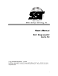
User’s Manual
Boot Strap Loader
Demo Kit
© 2001 Silicon Storage Technology, Inc. 414-01 7/01
The SST logo and SuperFlash are registered trademarks of Silicon Storage Technology, Inc. FlashFlex, In-Application
Programming, IAP and SoftLock are trademarks of Silicon Storage Technology, Inc. These specifications are subject to
change without notice.
1
User Manual for the FlashFlex Boot-Strap Loader Demo Kit
(P/N: SST89CK77BSL)
Introduction ………………………………………………………………………….…. 4
Getting Started …………………………………………………………………………
Unpacking the Demo Kit ………………………………………………………
System Requirements …………………………………………………………..
Windows 95/98/Me ………………………………..……………………
4
5
5
5
Connecting the System ………………………………………………………………... 5
Hardware Description ………………………………………………………………….
Jumpers ………………………………………………………………………...
MCU …………………………………………………………………………...
Clock …………………………………………………………………………..
Power ………………………………………………………………………….
Reset …………………………………………………………………………..
RS-232 ………………………………………………………………………...
LEDs …………………………………………………………………………..
External Flash Memory Chip ………………………………………………….
6
6
7
7
7
7
7
7
7
Installing the Software ………………………………………………………………… 8
Windows 95/98/Me ……………………………………….………….………… 8
How to Use the Software ………………………………………………………….…… 8
Set up Demo System ………………………………………………………….... 9
Configure COM Port & Baud Rate …………………………………………….. 10
Select Chip Type in External Memory Mode ………………………………….. 10
Erase All MCU Flash Memory ……………………………………………….. 11
Download the BSL Code into Block 1 Flash Memory ……………………….. 12
Activate Memory Re-mapping in External Memory Mode ……………….….. 12
Switch to Internal Memory Mode ………………………………………….…. 13
Download/Execute a Demo Program in Internal Memory Mode .….…….…... 14
Re-detect Chip Type …………………………………………………………… 15
Read Flash Memory ……………………………………………………………. 15
Compare Flash Memory with Hex/Binary File …………………………….….. 16
Save (Upload) Flash Memory into Disk File …………………………………... 16
Demo Software ………………………………………………………………………..
Twoball ………………………………………………………………………..
Binctr .………………………………………………………………………..
Pendb .………………………………………………………………………..
17
17
17
18
2
MCU Firmware ………………………………………………………………………… 19
External Memory Mode ………………………………………………………... 19
Internal Memory Mode …………………………………………………….…... 19
A. START Routine ……………………………………………………………. 20
B. INIT Routine ………………………………………………………………. 20
C. LOOP Routine ……………………………………………………………... 20
D. Pseudo IAP Routines …………………………………………………….… 20
E. Pseudo IAP Subroutines ………………………………………………….... 20
F. RESETVAL Routine …………………………………………………….… 21
G. Resources Used by Firmware ……………………………………………… 21
BSL Windows Software ……………………………………………………………….. 21
Self-detection of Serial Link ………………………………………………….... 21
Start/Stop/Re-start w/o Touching Any Hardware ……………………………… 21
Figures
Fig. 1 BSL Demo Board External Interfaces …………………………………… 5
Fig. 2 BSL Demo Board Components ………………………………………….. 6
Fig. 3 Jumper Setting of BSL Demo Board for External Memory Mode ………. 9
Fig. 4 Jumper Setting of BSL Demo Board for Internal Memory Mode …….... 13
Fig. 5 SST BSL v1.1E & Usage of Memory Remap in 89C5x Chip ………….. 22
Fig. 6 Firmware Routines of BSL v1.1E ………………………………………. 23
Fig. 7 Memory Map of Ext. Mem. Mode in SST39SF010 MPF Chip ………… 24
Fig. 8 Memory Map of Int. Mem. Mode in SST89C5x MCU Chip …………… 25
Appendix
A. File Name Convention …………………………………………………….. 26
B. List of Source Code ……………………………………………………….. 27
C. Pseudo Command Sequences ……………………………………………… 28
3
Introduction
The User Manual for the FlashFlex Boot-Strap Loader (BSL) Demo Kit provides the
user with the detailed information to quickly learn and use the kit. The manual, written
for the user of Windows 95/98/Me, walks the user through getting started, system
connections, hardware/MCU firmware description, installing the software, how to use the
software, a description of the demo software, and a step-by-step procedure for a quick
demo.
The MCU firmware/Windows software mentioned in this manual are BSL v1.1E. This
Kit contains a SST89C58 MCU, and all software code references are for that chip. For
future upgrades to this document, visit the MCU page on the SST website, which is
www.SuperFlash.com.
Getting Started
Unpacking the Demo Kit
The demo kit consists of the following items:
1. Hardware
• BSL Demo Board
• 6-ft. DB-9 RS-232 Cable
• AC Adapter
2. Floppy Disk – v1.1E(Windows 95/98/Me), with the following contents:
• Three demo programs (.a51 and .hex) - reside in folder “DemoProgram”:
- binctr.a51/.hex
- twoball.a51/.hex
- pendb.a51/.hex
The demo programs (.hex) are to be downloaded from the PC.
• External Memory Mode BSL v1.1E program – resides in folder
“ExtMemMode”:
- f51eble3.a51/.hex
The hexadecimal code (.hex) needs a programmer to reprogram it into the
external flash memory chip U3 (SST39SF010 MPF) located on the demo
board.
• Internal Memory Mode BSL v1.1E program – resides in folder
“IntMemMode”:
- f51mble3.a51/.bin/.hex
If the binary code (.bin) is downloaded, it is sent to block 1 flash memory,
or if the hexadecimal code (.hex) is downloaded, it is sent to block 0 flash
memory. The program code is configured for 11.0592 MHz, 38.4 Kbps
Baud operation with an 89C58 device.
4
• Windows 95/98/Me executable code (BSL v1.1E) – reside in root
directory:
- SSTFlashFlex51.exe
The PC executable code (.exe) is designed for Windows 95/98/Me.
Two MFC library files, Mfc42.dll and msvcrt.dll, are associated with PC
executable code and can be downloaded from SST website:
www.SuperFlash.com.
• Documentation
- Bsl_kit_UserManual.pdf
- Bsl_schematic.pdf
The bsl_schematic.pdf provides the circuit diagram of the BSL Demo
Board.
3. CD-ROM – µVision 2, a KEIL Development Tools for 8051, 251, USB, and
166 MCU families. For more information, please check KEIL website:
www.keil.com.
System Requirements
Windows 95/98/Me
The minimum hardware and software requirements are:
• Processor: Pentium or above
• RAM: 32 MByte
• Hard Disk Free Space: 2 MByte
• Operating System: Windows 95/98/Me
Connecting the System
RS
232
RS-232 Cable
COM1-4
Demo
Board
PC
Power
Conn.
SST BSL 1.0
AC
Adapter
414 ILL F01.1
Figure 1. BSL Demo Board External Interfaces
5
Figure 1 shows the connections required to run the BSL Demo Board. The kit AC
Adapter, with a standard 0.2178 in.(5.5 mm) OD and 0.098 in.(2.5 mm) ID barrel
connector, provides the DC power to run the board. The connector is inserted into the
board power connector as shown. The specifications for the AC adapter are:
AC Input:
120 VAC, 60 Hz, 6 Watts
DC Output:
9 V, 300 mA
The 6 ft. DB-9 RS-232 serial cable (male/female) is next installed between the demo
board and the COM1/COM2/COM3/COM4 port of the interfacing PC. The hardware
connections are now complete, and the system is ready for software operation, which is
discussed below.
Hardware Description
In Figure 2 is shown the major components of the BSL Demo Board. Now the different
board functions are briefly explained. The detailed circuit schematic is presented in the
document file Bsl_schematic.pdf.
JP2 JP3 JP1
3
2
1
Y1
U1
Jumpers
LEDs U2
D8
U6 RS-232
Conn.
U3
U4
Power
Conn.
U5
D1
RESET
U7
LED
S1
D11
SST BSL 1.0
414 ILL F02.0
Figure 2. BSL Demo Board Components
Jumpers
The following table lists the default and alternative settings of the individual jumpers:
Jumper Settings:
Jumper
Default Setting
Alternate Setting
JP1*
Don’t care
Don’t care
JP2
(2+3): EA# = 1
(1+2): EA# = 0
Internal Flash Active
External Flash Active
JP3
(closed) LEDs D1-D8 are
(open) LEDs D1-D8 are not
connected to Port 1
connected to Port 1
*JP1: CLOSED (P1.0 = 0), OPEN (P1.0 = 1).
6
MCU
There are two MCU sockets on the board: a PLCC socket (for U4) and a PDIP ZIF
socket (for U1). The board connections between sockets are in parallel, so that a MCU in
either socket can be used for a BSL demonstration.
Clock
On the demo board, a fixed clock frequency of 11.0592 MHz is derived by attaching
crystal Y1 to the internal oscillator of the MCU. Internal components of the MCU,
associated with the baud rate, are selectively programmed during system initialization
according to precalculated values dictated by the operating frequency. For that reason,
the crystal is soldered onto the board to insure that a reliable serial data communication is
maintained.
Power
+5V board power is derived from an on-board regulator circuit, centered upon the
LM7805C or equivalent voltage regulator chip (U7). The kit AC adapter transforms its
120VAC input into a +9V DC output, which is fed into the Power Connector on the
board and provides the input to the regulator circuit.
Reset
A hardware reset is accomplished using a dedicated reset chip (U5), either a DS1706L or
a MAX813LCP. When the Reset button (S1) is pressed, the RST output signal from U6
goes to a logic High to reset the MCU. The user needs to hold down the Reset button
while changing any jumper setting.
RS-232
Serial communication between the PC and the Receive (P3.0 RxD) and Transmit (P3.1
TxD) pins of the MCU utilizes an RS-232 Interface chip (the MAX232ACP chip in U6)
to perform the signal level shifting required for RS-232.
LEDs
Jumper JP3 enables or disables power to the eight (8) LEDs, which are tied to the Port 1
pins. The LEDs can be operated singly or together to provide user visibility of software
operation.
External Flash Memory Chip
The program in the External Flash Memory Chip (U3) allows the IAP commands
executing from the external memory device to program block 0 and 1 of the MCU (U1 or
7
U4) internal flash memory. This function allows the PC executable code to download the
BSL code into block 1 of the MCU internal flash memory. Jumper settings for the IAP
commands operation are: JP2 = (1+2) and JP1 can be either open or closed.
Note: If a SST89C54/58 MCU chip is in Level 4 Security Lock, then IAP operation
is inhibited.
Installing the Software
Windows 95/98/Me
To install the executable software on the PC, insert the kit’s floppy disk (labeled as
v1.1E) into the floppy drive of the PC. Next perform the following steps:
1) Create a new folder, e.g. SSTBSL_v11E, and copy the following file(s) into it:
SSTFlashFlex51.EXE
MFC42.DLL*
MSVCRT.DLL*
*Copy this file when Windows’ Operating System error message asks for
it. See Step 1-7 in next section for a description of the error message.
2) Copy the following folders from v1.1E floppy disk into the new folder:
ExtMemMode
IntMemMode
DemoProgram
How to Use the Windows Software
The MCU is an SST89C54/58 Rev.C1 or later and "unlocked". The following twelve
steps walk the user through the software.
1. Set up the demo system in External Memory Mode.
2. Configure the COM port and baud rate in host PC.
3. Select the chip type and the External Memory Mode.
4. Erase all MCU flash memory.
5. Download the BSL code into block 1 flash memory.
6. Activate memory re-mapping.
7. Switch to Internal Memory Mode.
8. Download/Execute the demo program in Internal Memory Mode.
9. Re-detect the chip type.
10. Read the flash memory.
11. Compare the flash memory with a hex/binary file.
12. Save (Upload) the flash memory into a disk file.
8
Step 1. Set up the Demo System in External Memory Mode.
SST BSL DEMO BOARD
JUMPER SETTING FOR
EXTERNAL MEMORY MODE
(EXECUTE IAP CMD)
JP2
JP3
JP1
3
2
1
ON: LED
DON'T CARE
2-3: EA#=1
1-2: EA#=0
Figure 3. Jumper Setting of BSL Demo Board for External Memory Mode
Make the above jumper settings for External Memory Mode operation.
1-1. Check that the SST89C58 (PDIP) chip is inserted correctly in the ZIF socket (U1) –
the notch of chip lines up with the latch handle of socket.
1-2. Insure the SST39SF010 MPF (PLCC) chip is firmly inserted into the PLCC socket
(U3).
1-3. Connect the serial cable between the Demo board and the COM port of user PC.
1-4. Connect the barrel connector to the board and plug the AC adapter into an AC power
source. The red power indicator on the Demo Board should be ON.
1-5. Load program files from Floppy Disk into user PC. Refer to the above section of
“Installing the Software”.
1-6. Click on the executable file SSTFlashFlex51.EXE to run the BSL v1.1E program
and display the Entry Menu.
1-7. If Window’s Operating System displays the following error message, the user needs
to copy two Microsoft Library files MFC42.DLL and MSVCRT.DLL, from the
SST website into the same folder as the executable file and restart the BSL
executable program.
The following Entry Menu will appear:
9
Step 2. Configure the COM port and the Baud rate.
2-1. Click on the RS232 menu and select the desired COM port and baud rate:
Above the main menu option, there is a message to remind the user that the selected
baud rate must match the baud rate pre-programmed in MCU firmware.
2-2. The RS-232 configuration is saved into a text file, SstBslComDft.txt, at the root
directory of C drive. This saved configuration becomes the default settings for later use.
Step 3. Select the Chip-type and the External Memory Mode.
3-1. Click on the ChipType then select “ChipType(v1.1E) – External MemMode
(EA#=0)” from the drop-down sub-menu. Select “Chip Type” and “External Memory
Mode”. Then click on OK to exit menu.
10
The following menu for External Memory Mode will appear:
Step 4. Erase the Entire Flash Memory in External Memory Mode
4-1. Click on Chip Erase function and click on Yes when Windows asks: “Do you
really want to proceed?”
4-2. Click on OK to exit Chip Erase when the message “Chip erase completed!”
appears.
4-3. Next reset the Demo board.
4-4. Follow the procedures of Step 3 above and select “Chip Type” and “External
Memory Mode” again after resetting the board.
11
Step 5. Download the BSL Code into Block 1 Flash in External Memory Mode
5-1. Click on Download, then select the appropriate File Name and Starting Sector. The
BSL binary code, F51MBLE3.BIN which is stored in the folder of IntMemMode, needs
to be downloaded into block 1 at address F000h. The user needs to scroll down the list
box of Starting Addresses and click on “Sector 000 Addr=F000”. Click on OK.
5-2. Click on Yes when the program warns the user and asks whether to proceed with the
download.
Step 6. Activate Memory Remapping in External Memory Mode
6-1. Click on Memory Remap, then select the Remap 1 KByte option and click OK.
6-2. Click Yes to redirect address range 0000h-03FFh to F000h-F3FFh when Windows
asks: “Do you really want to proceed?”
6-3. Click OK to exit menu when the message “Memory Remap Completed” appears.
To activate the 2 KB(Prog-RB1) re-mapping, the user needs to erase entire chip first, then
follows above steps 3, 5 and 6 to click on “Remap 2 Kbyte(PROG-RB1)”.
12
Step 7. Switch to Internal Memory Mode
SST BSL DEMO BOARD
JUMPER SETTING FOR
INTERNAL MEMORY MODE
(EXECUTE IAP CMD)
JP2
JP3
JP1
3
2
1
ON: LED
DON'T CARE
2-3: EA#=1
1-2: EA#=0
Figure 4. Jumper Setting of BSL Demo Board for Internal Memory Mode
7-1. Click on yellow CLR radio button to erase the chip information.
7-2. Hold down the Reset button then change the jumper settings as shown in the above
figure to enter Internal Memory Mode.
7-3. Click on “Auto DetectChip” then select “Detect Chip Type (v1.1E) - Internal
Memory Mode (EA#=1)”. Click on OK then wait for two seconds to allow the program
to automatically detect the board. Reset the board only if the detection failed the two
seconds window. The time slot for the whole detection is six seconds.
7-4. The chip-type and firmware version were pre-programmed into block 1 flash
memory.
The following menu for Internal Memory Mode will appear:
13
Step 8. Download/Execute the Demo or User Program in Internal Memory Mode
8-1. Click on Dnload/Run UserCode, enter the Start Address (Sector 000 Addr=0000)
and File Name, e.g. Binctr.hex. Click OK to download code.
8-2. Prior to downloading, the sectors in block 0 matched the code size are to be erased.
Click on Yes to accept and to continue the code downloading.
8-4. Each demo program will light the LEDs in a unique pattern.
8-5. The Run UserCode command resets all SFRs in MCU chip to their default values
and then executes user code at address 0000h in block 0.
8-6. In six to eight seconds, a warning message shown to warn the user about the lost of
serial link to the MCU chip and the chip information is erased.
14
Step 9. Re-detect the Chip.
To continue further IAP operations after the execution of RunCode command, the user
needs to re-detect the Chip-type by repeating “Step 7-3”.
Step 10. Read Demo/User Code from Block 0 Flash in Internal Memory Mode
Click on Read, select the Start Address and Range (no. of sectors). Then click OK.
The Demo program Binctr.bin occupies two sectors, sector 000 and sector 006. User can
click on sector number and the content of selected sector is shown in lower half of
window.
15
Step 11. Compare Hex/Binary file with the flash
11-1. Click on File menu then the Compare option. The dialog window of IAP Status
shows the result of file comparision.
11-2. If comparing with a different demo software, e.g. Pendb.hex, an unmatching result
will be indicated instead.
Step 12. Save Data into a File (Upload) from Block 0 in Internal Memory Mode
12-1. To save data into a binary/text file, the user needs to click on File menu then the
Save option.
12-2. Enter a filename, choose the type of file (binary or text file), select the starting
address and number of sectors (in Range list box) then click OK. Click OK when the
message “Save data has completed” appears.
16
Demo Software
Three demo software programs have been supplied with the BSL Demo Kit, and the
intent here is provide the user with some understanding of their basic functionality. Any
one of them can be downloaded from the PC to the Demo Board, and executed there. For
a visible presence on the demo board, each of the demo routines manipulates the board
LEDs in some manner. The source (.A51) and download (.HEX) files for each of the
three software routines are included on the kit floppy disk.
The file names are:
1) TWOBALL.A51/.HEX
2) BINCTR.A51/HEX
3) PENDB.A51/HEX
TWOBALL
The “twoball” routine corresponds to a two-ball bouncing ball sequence, that is, the two
most significant LEDs will light up and proceed to shift right one LED bit position at a
specific time interval. When the lighted pair reaches the two least significant bit
positions, then they will begin to shift left in the same manner. The right-left sequence
will be continuous, and is illustrated in the following diagram:
TWOBALL DEMO:
PORT 1 BITs PL0
LED DISPLAYS D1
PL1
D2
PL2
D3
PL3
D4
LIGHT ON
PL4
D5
PL5
D6
PL6
D7
PL7
D8
414 ILL F03.0
BINCTR
The “binctr” routine shows a binary counting sequence on the LEDs, which are changing
at a specific time interval. Some of the counting states are illustrated in the following
diagram:
17
BINCTR DEMO:
PORT 1 BITs PL0
LED DISPLAYS D1
PL1
D2
PL2
D3
PL3
D4
PL4
D5
PL5
D6
PL6
D7
LIGHT ON
PL7
D8
414 ILL F04.0
PENDB
The “pendb” software routine causes the LEDs to behave similar to a pendulum. Like the
previous routines discussed, the LEDs are changing at a specific time interval visible to
the user. The LED pattern is shown in the following diagram:
PENDB DEMO:
PORT 1 BITs PL0
LED DISPLAYS D1
PL1
D2
PL2
D3
PL3
D4
PL4
D5
LIGHT ON
PL5
D6
PL6
D7
PL7
D8
414 ILL F05.0
18
MCU Firmware
The flowchart in Figure 5 provides an operational overview of the SST BSL v1.1E. This
BSL version applies only to the SST89C5x family of microcontrollers(MCU). As shown,
there are two operating modes in this version: Internal Memory Mode and External
Memory Mode. If the internal flash memory of the MCU doesn’t contain BSL code, then
the External Memory Mode must be used to program the internal flash memory.
Executing code from external flash memory, the BSL code or User code or a combination
of BSL and User code can be programmed into MCU flash memory blocks 0 and 1.
Once the BSL code is resident in block 1 and memory re-mapping(1KB/2KB/4KB) has
been activated, the Internal Memory Mode can be used.
Appendix A describes the file naming convention for the firmware. Appendix B lists the
hex file to be used to download into a SST39SF010 MPF chip and the hex/binary files to
be used to download into a SST89C5X MCU chip. For the 89C5X chip, the hex file
needs to be downloaded into address 0000h of block 0 and the binary file needs to be
downloaded into address F000h of block 1 respectively. Appendix C provides the list of
pseudo-command sequences (sent from the host PC to the MCU chip) after the serial link
is established.
External Memory Mode
For the External Memory Mode, the BSL-executed code is resident in an external
memory device (an external EEPROM, such as a SST39SF010 MPF chip). IAP
commands are executed from the external EEPROM to program blocks 0 and 1 of the
internal flash memory of the MCU. Figure 7 shows the memory map associated with this
mode.
Internal Memory Mode
Entry into the Internal Memory Mode is possible only if the following MCU
requirements are met: (1) BSL code must be resident in the MCU Block 1 flash memory,
(2) the MCU must not be hard locked, and (3) the MCU must default to a 1K re-map on
reset. Once the chip requirements are met, the BSL firmware can be entered by any one
of the following ways:
(a) Power cycle the system, which provides a power-on reset.
(b) With power on the system, push the reset button (hardware reset).
(c) Watchdog (WDT) timeout in user application code.
(d) Issue a branch instruction from within user code, for example:
MOV SFCF, #80h ; make block 1 flash visible
LJMP 0F000h
; enter BSL code
Executing IAP commands from block 1 flash, the user can program application code into
block 0 flash memory. The flowchart in Figure 6 provides an outline of firmware
routines. The BSL routines and the memory maps associated with this mode are shown
in Figure 8. A brief description of firmware features and routines are listed below.
19
A. START Routine
The START routine checks the memory re-mapping and the Watchdog Timer(WDT).
Because the memory re-mapping is activated after a successful system reset, the interrupt
vector addresses in block 1 are used rather than in block 0. This routine decides where to
branch next in the code, and the selection is based on the detection of WDT Reset Flag
(WDTC.2):
WDTC.2 = 1: WDT timeout detected, the BSL code turns off the WDT if the chip
is re-mapped into 1 or 2 KB range or the BSL code turns on the WDT if the chip is remapped into 4 KB range. Then the BSL code jumps to RESETVAL routine to restore
power-on values into SFRs, and next jumps to 0000h of block 0 to execute the user coldstart routine.
WDTC.2 = 0: continue INIT routine and issue IAP commands as required.
B. INIT Routine
The INIT routine initializes the Special Function Registers(SFRs) and the stack
pointer(SP), uses MCU Timer2 for baud rate generation of the serial port, and sets the
WDT timeout for 50 ms(typical).
C. LOOP Routine
The LOOP routine sends a Query byte(F7h) to host PC and then waits for a pseudo-IAP
command sent from the PC before the WDT timeout.
D. Pseudo IAP Routines
The pseudo IAP routines include the handshaking, report chip ID and firmware ID, runuser-code and NOP.
In handshaking routine, the host PC sends two bytes – 05h and 55h – to MCU to establish
the serial link before WDT timeout in 50 ms(typical) occurrs. Once the serial link is
established, the MCU sends a status byte to PC, which contains the security bits(SB1/2/3)
and re-map bits(RB0/1), changes the WDT timeout to 2000 ms(typical) and then waits in
the BSL-LOOP routine for further pseudo IAP commands.
The run-user-code routine (command bytes: 62h and 62h) breaks the serial link and
jumps to the resetval routine.
If the command byte is 60h, the MCU sends the chip and firmware IDs to PC. Therefore,
the user needs to program the chip and firmware IDs in this routine.
E. Pseudo IAP Subroutines
The Inbyte and Outbyte subroutines use the polling rather than the interrupt algorithm to
handle the data receiving and transmission of the serial port.
The subroutines of handling four IAP operations are sector-erase, program-byte, burstbyte and verify-byte. Each IAP operation requires four bytes - command byte, highaddress byte, low-address byte and a counter-byte. Each operation needs to poll SFST.2
bit to check the completion of IAP operation.
20
F. RESETVAL Routine
This routine is called before executing user cold-start routine at 0000h of block 0. It
restores reset values into SFRs, sets the STRG string to “DONE”, sets the visibility bit
(SFCF.7) to a logical “high”, turns on the WDT if REMAP=4 KB or turns off the WDT if
REMAP=1 or 2 KB, disables the memory re-map, and then jumps to 0000h.
G. Resouces Used by BSL code
The BSL code needs to use registers A, B, DPTR, SFCF, and R0 – R6 in register bank 0
and the WDT. The internal RAM from 08h to 0Bh is used to store the string STRG. The
stack requires the internal RAM from 0Ch to 0Fh after the serial link is established and
the BSL is waiting to execute the IAP command.
If the BSL routines are called from user code, the user is required to save the contents of
above resources before branching to BSL routines and then restoring original values upon
returning from BSL routines. Additionally, the BSL writes a string “USER” into 08h0Bh of internal RAM to prevent the Watchdog Timer Reset Flag (WDTS) from being
cleared before returning to user code.
If the BSL is entered after a power-on-reset, the BSL writes a string “POWR” into 08h0Bh of internal RAM to allow the Watchdog Timer Reset Flag (WDTS) to be cleared
before returning to user code.
BSL Windows Software
Self-detection of Serial Link
The PC can detect whether the serial link is alive or not in a few seconds, namely two to
six seconds. After either a disconnection of serial link or an interrupt of dc power, the
software issues a warning message and erases the chip information on the screen.
Start/Stop/Re-start w/o Touching Any Hardware
If the chip is 4 KB re-mapped, BSL turns on the WDT before returning to user code. This
arrangement promises the MCU to run the user code for 2 seconds typically if BSL
routine is blocked by an interruption of serial link. Then the MCU issues a query
command to the PC and the PC can automatically re-establish the serial link after the
cause of interruption is fixed.
After returning from BSL routines to the user code, the user needs to constantly refresh
the WDT in user code to prevent the WDT expiration during normal operation of user
code.
21
START
BSL v1.1E
in Host PC
Yes
Is
BSL On-Chip
?
No or Don't Know
External Memory Mode
Is
On-Chip BSL
Baudrate setting
correct
?
(BSL v1.1E in SST39SF010)
No
Tools for Downloading
BSL v1.1E into SST89C5x
1. SST BSL Demo Kit
2. Phytec Evaluation Kit
3. Universal Programmer
Yes
Chip-Erase
Internal Memory Mode
(BSL v1.1E in SST89C5x)
Turn off both memory
re-mapping and
security-lock features
Executable IAP Functions
Download Code
Type
1. Compare Hex/Binary file with
flash contents in block 0,1
2. Download User code to block 0
3. Erase sectors in block 0
4. Read flash contents in block 0, 1
5. Save flash contents in block 0,1
into a disk file
BSL Code
Only
Download BSL
code to block 1
BSL+User
Code
Download user
code with
embedded BSL
code to blocks 0, 1
Advise user to
RESET chip to turn
on memory remapping feature
automatically
User Code
Only
Download user
code to blocks 0, 1
Activate Memory
Re-mapping
The amount of memory
re-mapped depends on
BSL code in block 1:
1 KB, 2 KB or 4 KB
FIG.5 SST Boot-Strap Loader v1.1E and Usage of Memory Re-mapping
in SST89C5x MCU
22
START
BSL v1.1E in
SST89C5x
Is
WDT Timeout
(WDTC.2=1)
?
No
START Routine
Is
Chip Re-mapped
?
No
Set STRG to "RMAP"
Yes
Is
STRG="POWR"
?
Yes
No
Is
STRG=
"USER"
?
No
Set STRG to "POWR"
Yes
INIT Routine
1. Set UART to 38.4 Kbps
Baudrate
2.Set WDT to timeout in 50
ms
3. Set SP to 0Bh
Clear WDTC.2
Yes
RESETVAL Routine
Is
No
STRG=
"RMAP"
?
Yes
Set WDT to timeout in
10 ms
Clear
WDTC.2
LOOP Routine
Is
Re-mapped
to 4KB
?
Yes
No
Turn on WDT
Software Trap
Send Query CMD
(F7h) to Host PC
No
Set STRG
to "USER"
1. Restore reset values to
SFRs
2. Set STRG to "DONE"
3. Set VIS=1 & REMAP=0
KB
4.Jump to 0000h to execute
Usercode
Recv'd CMD
from Host PC
?
Yes
Refresh WDT
No
Handshaking
1.CMD: 05h,55h
2.Send Status
byte to host PC:
SB3/2/1, RB1/0
3.Set WDT=
2000 ms
Request
Device ID &
MCU
Firmware
version
CMD: 60h
NOP CMD
1. CMD: 61h
2. Refresh
WDT
Valid CMD
?
Yes
Call Resetval
routine to run
user code
CMD:
62h,62h
(IAP CMD Subroutines)
Burst Pgm
CMD:
06h,XXh,YYh
,ZZh
Sector Erase
CMD:
0Bh,XXh,YYh
,ZZh
Verify Byte
CMD:
0Ch,XXh,YYh
,ZZh
Byte Pgm
CMD:
0Eh,XXh,YYh
,ZZh
LOOP Routine
FIG.6 MCU Firmware Routines of SST Boot-Strap Loader v1.1E
23
39SF010
(128K x 8)
00000h
VECTOR TABLE
Assign BSL_START routine to
00040h
DESIGN NOTES FOR USING 39SF010 AS
EXTERNAL ROM
0003Fh
00040h
A. BSL-START ROUTINE
Initialize SFRs & set up serial port
B. BSL-LOOP ROUTINE
Wait for pseudo IAP cmd sent by
host PC.
C. PSEUDO IAP ROUTINES
Hand-shake (05h)
D. PSEUDO IAP SUBROUTINES
1. Out-byte: transmit a byte thru
serial port
2. In-byte: receive a byte from
serial port
3. Chip-erase: erase entire chip
4. Block-erase: erase block 0/1
5. Sector-erase: erase a sector
6. Program-byte (write)
7 Burst-program (burst write)
8. Verify-byte (read)
9. Security-lock
10. Remap
11. Done?: poll SFST.2 to check
the completion of flash operation
1. Connect WE# pin to VDD to disable
Wrtie_enable.
2. Connect CE# pin to GND to enable
Chip_enable.
3. Connect OE# pin to PSEN# of SST 89x5x
chip.
4. Connect A16 to GND if user plans to map
the lower half of chip (from 00000h to 0FFFFh)
as external ROM. Otherwise, connect A16 to
VDD to map upper half of chip (from 10000h to
1FFFFh) as external ROM.
001FFh
00200h
Area not been used are available
for future expansion
1FFFFh
FIG. 7 Memory Map of External Memory Mode (BSL v1.1E)
in SST39SF010 MPF
24
BLOCK 0(C54 CHIP, 16 KB FLASH)
(128 bytes/sector)
BLOCK 1(C54/C58, 4 KB FLASH)
(64 bytes/sector)
SECTOR #
0
0000h
DESIGN NOTES
1. Download user code
from sector#0 to the
end.
2. User code available
range : 0000 - 3FFFh
or 16 KB.
3FFFh
127
BLOCK 0(C58 CHIP, 32 KB FLASH)
(128 bytes/sector)
SECTOR #
0
0000h
DESIGN NOTES
1. Download user code
from sector#0 to the
end.
2. User code available
range : 0000 - 7FFFh
or 32 KB.
7FFFh
255
F000h
SECTOR #
0
VECTOR TABLE
1. Assign BSL-START routine to F040h.
2. Continue BSL if REMAP=1/2/4 KB or stay in
F03Fh a software trap if REMAP=0KB
1
F040h
A. START ROUTINE
Check WDTC.2 (WDT reset flag):
WDTC.2=1: WDT timeout detected,
1. turn off WDT if REMAP=1 or 2 KB,
2. turn on WDT if REMAP=4KB.
3. Jump to RESETVAL routine & then start
user cold-boot routine at address 0000h.
WDTC.2=0: Continue INIT routine.
B. INIT ROUTINE
1. Initialize SFRs.
2. Set up serial port, baudrate=38.4 Kbps.
3. Set SP=0Bh.
C. LOOP ROUTINE
Send a Query cmd(F7h) to host PC & wait for
pseudo IAP cmd from host PC.
D. PSEUDO IAP ROUTINES
1. Hand-shake (05h & 55h).
2. Report Chip-ID & FW-ID (60h) User needs
to set up Chip-ID & FW-ID in this routine.
3. Run-usercode (62h & 62h) - jump to
RESTVAL ROUTINE.
4. NOP cmd: refresh WDT.
E. PSEUDO IAP SUBROUTINES
1. Out-byte/In-byte: transmit/receive a byte
thru serial port.
2. Sector-erase: erase a sector.
3. Program-byte (write).
4. Burst-program (burst write).
5. Verify-byte (read).
6. Done?: poll SFST.2 to check the completion
of flash operation.
F. RESETVAL ROUTINE
1. Restore reset values to SFRs.
2. Set STRG to "DONE".
3. Set VIS=1 & REMAP=0KB.
4. Jump to 0000h to run usercode.
G. RESOURCES USED BY FIRMWARE
1. Registers R0-R6 in register bank 0.
2. Rgisters A, B, DPTR, SFCF
3. Internal RAM 08h-0Bh used by STRG string
4. Internal RAM 0Ch-0Fh used by stack.
F3FFh 5. Watchdog Timer (WDT).
15
F400h
16
Area not been used by BSL are
available for user or for future BSL expansion
FFFFh
63
FIG. 8 Memory Map of Internal Memory Mode (BSL v1.1E)
in SST89C5x MCU
25
APPENDIX A. File Name Convention
The BSL file name convention has been adopted to accommodate improved software
versions, additional chip types and frequencies, memory mode and custom boot-strap
loaders for the FlashFlex MCU family. The file name format is:
File Name:
F51xBLyz.ext
where x =
P for MS-DOS, PC-resident code
M for MCU-resident code in Internal Memory
Mode
C for Custom MCU-resident code
y=
BSL/EasyIAP Version Number for x = P
A = Version 1.0
B = Version 1.1/ 2.0
C = Version 1.2
y=
Chip Type and Frequency for x = M
E = C58 11.0592 MHz
F = C58 12 MHz
G = C54 11.0592 MHz
H = C54 12 MHz
(etc.)
y=
Customer ID for x = C
A = Infronex C58 7.3728 MHz
B = (next customer)
Revision No.
0 = Original Release
1 = First Revision
(etc.)
z=
26
APPENDIX B. List of Source Code
The BSL source code now consists of two parts: for the Window 95/98/Me-resident
software, an executable file (SSTFlashFlex51.EXE) is supplied, and for the MCUresident code, the source files (.A51), an Intel hex file (.HEX) and a binary file (.BIN) are
furnished. The table below lists the files that can be downloaded from the SST website.
Both 11.0592 MHz and 12.0 MHz versions use MCU Timer 2 for baud rate generation
for the serial port.
Table B1. BSL Files for Both Internal and External Memory Modes
Chip Type
Ext. Crystal
Baud Rate
PC Files
MCU Files
Frequency
89C58
11.0592
38.4K/19.2K/9.6 SSTFlashFlex51.
F51MBLE3.A51
MCU
MHz
K/4.8K/2.4K
EXE
F51MBLE3.HEX*
(Internal
F51MBLE3.BIN*
Memory
12.0 MHz 38.4K/19.2K/9.6 SSTFlashFlex51.
F51MBLF3.A51
Mode)
K/4.8K/2.4K
EXE
F51MBLF3.HEX*
F51MBLF3.BIN*
89C54
11.0592
38.4K/19.2K/9.6 SSTFlashFlex51.
F51MBLG3.A51
MCU
MHz
K/4.8K/2.4K
EXE
F51MBLG3.HEX*
(Internal
F51MBLG3.BIN*
Memory
12.0 MHz 38.4K/19.2K/9.6 SSTFlashFlex51.
F51MBLH3.A51
Mode)
K/4.8K/2.4K
EXE
F51MBLH3.HEX*
F51MBLH3.BIN*
39SF010
11.0592
38.4K/19.2K/9.6 SSTFlashFlex51.
F51EBLE3.A51
MPF
MHz
K/4.8K/2.4K
EXE
F51EBLE3.HEX*
(External
Mem Mode)
* Binary file should be downloaded into block 1 and starts at address F000h. Hence, Hex file should be
downloaded into block 0 at address 0000h.
27
APPENDIX C. PSEUDO COMMAND SEQUENCES
The following table lists the pseudo-command sequences sent from the host PC to the
SST89C5x MCU. The code in MCU chip decodes the pseudo-command sequence and
executes IAP command accordingly.
Table C1. Pseudo IAP Command Sequence (all values are in Hex format)
HOST PC ßà
89C5x(INT)/
39SF010(EXT)
Chip-Erase
Memory
Mode
Pseudo CMD
Sequence
(Host PC)
EXT
01 00 00 01
Memory-Remap
Prog-RB0
Prog-RB1
Security-Lock
Prog-SB1
Prog-SB2
Prog-SB3
Handshaking
Handshaking
Burst-Program
EXT
EXT
EXT
EXT
EXT
EXT
EXT
EXT
INT
INT/EXT
02
02
02
04
04
04
04
05
05
06
Sector-Erase
INT/EXT
OB XX YY ZZ
0B
Byte-Verify
INT/EXT
0C XX YY ZZ
0C
Block-Erase
Byte-Program
INT/EXT
INT/EXT
0D XX 00 01
0E XX YY ZZ
0D
0E
Device code &
FW version
Run-UserCode
Query Byte
INT
60
None
INT
INT
62 62
F7
None
None
XX
00
01
XX
00
01
02
55
XX YY ZZ
IAP
CMD
(MCU)
01
08
09
0F
03
05
None
None
06
Description of Pseudo CMD
Sequence
Erase flash contents, re-map &
security-lock bits
XX=00/01, set RB0/RB1
MCU execute IAP CMD: 08
MCU execute IAP CMD: 09
XX=00/01/02, set SB1/SB2/SB3
MCU execute IAP CMD: 0F
MCU execute IAP CMD: 03
MCU execute IAP CMD: 05
One-byte CMD
Two-byte CMD
XX/YY/ZZ: Addr-Hi/Addr-Lo/No. of
bytes in a ROW(half of a sector)
XX/YY/ZZ: Addr-Hi/Addr-Lo/SectorCount
XX/YY/ZZ: Addr-Hi/Addr-Lo/No. of
Sector Bytes
XX=00/F0: BLK 0/BLK 1
XX/YY/ZZ: Addr-Hi/Addr-Lo/No. of
Sector Bytes
User needs to pre-program Device
code & FW version in v1.1E code
Run user code
MCU is ready to receive CMD
28