1
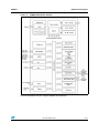
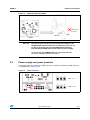
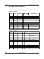
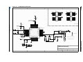
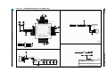
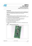
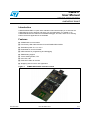
UM0817
User Manual
STM8S-DISCOVERY
evaluation board
Introduction
STM8S-DISCOVERY is a quick start evaluation board which helps you to discover the
STM8 features, and to develop and share your own application. It is based on an
STM8S105C6T6 and includes an embedded debugger, ST-LINK, and a touch sensing
button. Numerous applications are available.
Features
■
STM8S105C microcontroller
■
Powered by USB cable between PC and STM8S-DISCOVERY
■
Selectable power of 5 V or 3.3 V
■
Embedded ST-Link for STM8S
■
USB interface for programming and debugging
■
SWIM debug support
■
Touch Sensing button, TS1
■
User LED, LD1
■
Extension header for all I/Os
■
Wrapping area for users own application
Figure 1.
October 2009
STM8S-DISCOVERY evaluation board
Doc ID 16361 Rev 1
1/17
www.st.com
Contents
UM0817
Contents
1
Quick start . . . . . . . . . . . . . . . . . . . . . . . . . . . . . . . . . . . . . . . . . . . . . . . . . 3
2
Hardware and layout . . . . . . . . . . . . . . . . . . . . . . . . . . . . . . . . . . . . . . . . . 4
2.1
STM8S105C6 microcontroller . . . . . . . . . . . . . . . . . . . . . . . . . . . . . . . . . . 6
2.2
ST-Link . . . . . . . . . . . . . . . . . . . . . . . . . . . . . . . . . . . . . . . . . . . . . . . . . . . . 8
2.2.1
Using the ST-Link . . . . . . . . . . . . . . . . . . . . . . . . . . . . . . . . . . . . . . . . . . . 8
2.2.2
Using the ST-Link on other applications . . . . . . . . . . . . . . . . . . . . . . . . . . 8
2.3
Power supply and power selection . . . . . . . . . . . . . . . . . . . . . . . . . . . . . . . 9
2.4
Single touch sensing . . . . . . . . . . . . . . . . . . . . . . . . . . . . . . . . . . . . . . . . 10
3
Daughter board connection . . . . . . . . . . . . . . . . . . . . . . . . . . . . . . . . . . 11
4
Electrical schematics . . . . . . . . . . . . . . . . . . . . . . . . . . . . . . . . . . . . . . . 13
5
Revision history . . . . . . . . . . . . . . . . . . . . . . . . . . . . . . . . . . . . . . . . . . . 16
2/17
Doc ID 16361 Rev 1
UM0817
1
Quick start
Quick start
It is very simple to get started using the STM8S-DISCOVERY evaluation board, just follow
these four steps:
1.
Connect the STM8S-DISCOVERY board to a PC with a USB cable.
2.
Press the TS1 button, Observe LED LD1 blinking.
3.
Press the TS1 button to change blinking speed.
4.
Connect to www.st.com/stm8s-discovery and follow the tutorial.
The STM8S-DISCOVERY evaluation board helps you to develop and share your own
application. You can discover more of the STM8S features by downloading and executing
the proposed programs in the project list.
Doc ID 16361 Rev 1
3/17
Hardware and layout
2
UM0817
Hardware and layout
The STM8S-DISCOVERY evaluation board is designed around the STM8S105C6
microcontroller in an LQFP48 package. It has two distinct sections that may be separated,
the STM8S105C6 module and the ST-Link module.
Figure 2 illustrates the connections between the STM8S105C6 and its peripherals (STLINK, touch-sensing button, LED and connectors).
Figure 3 helps you to locate these features on the STM8S-DISCOVERY board, as well as
the potential point of separation (for more details refer to Section 2.2.2: Using the ST-Link on
other applications).
Figure 2.
4/17
Hardware block diagram
Doc ID 16361 Rev 1
UM0817
Hardware and layout
Figure 3.
Top layout
USB connector
ST-LINK module
ST-Link JTAG
USB data transfer LED
ST-LINK core
SWIM connector
Possible separation point
LED (LD1)
Power supply jumper
External Osc. (16 MHz)
STM8S105C6 module
STM8S105C6
Touch sensing button (TS1)
Wrapping area
SO16 footprint
Doc ID 16361 Rev 1
5/17
Hardware and layout
2.1
UM0817
STM8S105C6 microcontroller
Figure 4.
STM8S105C6 package
The STM8S105C6 8-bit microcontroller offers:
32 Kbytes of Flash program memory, and
1 Kbyte true data EEPROM.
This device provides the following benefits:
●
●
●
●
●
6/17
Reduced system cost
–
Integrated true data EEPROM for up to 300 K write/erase cycles
–
High system integration level; internal clock oscillators, brown-out reset, watchdog.
Performance and robustness
–
16 MHz CPU clock frequency
–
Up to 38 I/Os on a 48-pin package including 16 high sink outputs
–
Robust I/O immune against current injection
–
Independent watchdogs with separate clock source
–
Flexible clock control, 4 master clocks (HSI, LSI, HSE and external HSE)
–
Clock security system
–
A family of products for applications with 2.95 V to 5.5 V operating supply
Short development cycles
–
Applications scalability across common family product architecture with
compatible pinout, memory map and modular peripherals.
–
Full documentation and a wide choice of development tools
–
Standard S/W library for firmware development quick start
–
Numerous application notes and firmware examples available
Product longevity
–
Advanced core and peripherals made in state-of-the-art technology
–
Low power modes (wait, active-halt, halt)
–
Auto wake-up timer for active halt
–
Permanently active, low consumption
Other features
–
Nested interrupt controller with 32 interrupts
–
Up to 37 external interrupts on 6 vectors
–
2 x 16-bit general purpose timers; with 2+3 CAPCOM channels (IC, OC or PWM)
–
Advanced control timer: 16-bit, 4 CAPCOM channels, 3 complementary outputs,
dead- time insertion and flexible synchronization
–
8-bit basic timer with 8-bit prescaler
–
UART with clock output for synchronous operation, Smartcard, IrDA, LIN
–
SPI interface up to 8 Mbit/s
–
I2C interface up to 400 Kbit/s
–
Analog-to-digital converter 10-bit, ±1 LSB ADC with up to 10 multiplexed channels
Doc ID 16361 Rev 1
UM0817
Hardware and layout
Figure 5.
STM8S105C6 block diagram
For more information see the complete STM8S documentation.
Doc ID 16361 Rev 1
7/17
Hardware and layout
2.2
UM0817
ST-Link
The ST-Link provides a USB interface for programming and debugging using a single wire
interface module (SWIM). The ST-Link module of the STM8S-DISCOVERY evaluation board
also supplies 5 V and 3.3 V to the STM8S105C6 module.
2.2.1
Using the ST-Link
Figure 6.
Typical configuration
Hardware requirements:
- USB cable type A to B
- Computer with Windows 2000, XP or Vista OS
Software requirement:
Programming tool chain supporting ST-Link SWIM
Note:
The driver for ST-Link is installed automatically when the USB is connected.
For more information about ST-Link debugging and programming features refer to the
software and debug documentation.
For information about the SWIM protocol, refer to UM0470.
2.2.2
Using the ST-Link on other applications
You can connect your ST-Link to other applications in 2 ways.
●
By removing the solder bridges: This way uses the ST-Link without breaking the PCB:
Unsolder the two solder bridges SB1 and SB2 under the SWIM connector. See
Figure 7. You can re-solder the two bridges at a later date thus keeping the STM8SDISCOVERY usable.
●
By removing it from your board: This way constitutes a good alternative to programming
the STM8 devices in other applications. See Figure 8.
Figure 7.
ST-Link alternative
Remove SB1 and SB2 solder bridges
8/17
Doc ID 16361 Rev 1
UM0817
Hardware and layout
Figure 8.
Separated ST-Link module
STM8S105C6
eval board
STLink
SWIM
Warning:
By removing this module you will lose power supply on the
STM8S105C6 evaluation board. In consequence, you will not
be able to program and use the STM8S105C6 evaluation
board without a SWIM cable and an external power supply.
To reconnect your STM8S105C6 use connector CNn see
Section 3: Daughter board connection.
2.3
Power supply and power selection
The power supply is provided by a USB connector. Jumper JP1 selects the VDD value (5 V
or regulated 3.3 V) see Figure 9.
Figure 9.
Power selection
VDD = 5 V
VDD = 3.3 V
Doc ID 16361 Rev 1
9/17
Hardware and layout
2.4
UM0817
Single touch sensing
A touch sensing button TS1 is available on the STM8S-DISCOVERY evaluation board (see
Figure 10).
Figure 10. Touch sensing schematic
To disable the touch sensing interface and to use PC1, PC2 and PC3 as standard I/O, you
need to unsolder the 2-1 connection and solder 2-3 connection on SB4 and SB3, you also
need to unsolder the R2 resistor.
RC acquisition principle
The RC acquisition method detects a human touch on key touch sensor (TS1) by measuring
the small variation of the touch electrode capacitance (C2). Electrode capacitance C2 is
periodically charged and discharged through a fixed resistor (R2).
The capacitance value depends on the following parameters: electrode area (A), relative
dielectric constant of the insulator (eR), the relative permittivity of air (e0) and the distance
between the two electrodes.
For more information about touch sensing please refer to AN2927.
10/17
Doc ID 16361 Rev 1
UM0817
Daughter board connection
Four 12-pin male headers CN1, CN2, CN3 and CN4 are connected to the STM8S105C6
microcontroller. See the following tables for pin assignments.
CN1 pinout
Pin number Pin number
(Cn1)
(chip)
Pin name
Type
Table 1.
Main function
Alternate function
1
1
NRST
IO
Reset
2
2
OSCIN/PA1
IO
Port A1
3
3
OSCOUT/PA2 IO
Port A2
4
4
Vssio_1
S
I/O ground
5
5
Vss
S
Digital ground
6
6
VCAP
S
1.8V regulator capacitor
7
7
Vdd
S
Digital power supply
8
8
Vddio_1
S
I/O power supply
9
9
PA3
IO
Port A3
10
10
PA4
IO
Port A4
11
11
PA5
IO
Port A5
12
12
PA6
IO
Port A6
Table 2.
CN2 pinout
Pin number Pin number
(Cn2)
(chip)
Pin name
Type
3
Daughter board connection
Main function
Alternate function
1
25
PE5
IO
Port E5
SPI master / slave
2
26
PC1/TS1
IO
Port C1
Timer 1 - channel 1 / UART2
synchronous clock
3
27
PC2/TS1_load IO
Port C2
Timer 1 - channel2
4
28
PC3
IO
Port C3
Timer 1 - channel 3
5
29
PC4
IO
Port C4
Timer 1 - channel 4
6
30
PC5
IO
Port C5
SPI clock
7
31
Vssio_2
S
I/O ground
8
32
Vddio_2
S
I/O power supply
9
33
PC6
IO
Port C6
SPI master out / slave in
10
34
PC7
IO
Port C7
SPI master in / slave out
11
35
PG0
IO
Port G0
12
36
PG1
IO
Port G1
Doc ID 16361 Rev 1
11/17
Daughter board connection
CN3 pinout
Pin name
Main function
Alternate function
1
13
Vdda
S
Analog power supply
2
14
Vssa
S
Analog ground
3
15
PB7
IO
Port B7
Analog input 7
4
16
PB6
IO
Port B6
Analog input 6
5
17
PB5
IO
Port B5
Analog input 5
6
18
PB4
IO
Port B4
Analog input 4
7
19
PB3
IO
Port B3
Analog input 3
8
20
PB2
IO
Port B2
Analog input 2
9
21
PB1
IO
Port B1
Analog input 1
10
22
PB0
IO
Port B0
Analog input 0
11
23
PE7
IO
Port E7
Analog input 8
12
24
PE6
IO
Port E6
Analog input 9(2)
Type
Pin number Pin number
(Cn3)
(chip)
Type
Table 3.
UM0817
Main function
*
Table 4.
CN4 pinout
Pin number Pin number
(Cn4)
(chip)
12/17
Pin name
Alternate function
1
37
PE3
IO
Port E3
Timer 1 – break Input
2
38
PE2
IO
Port E2
I2C data
3
39
PE1
IO
Port E1
I2C clock
4
40
PE0
IO
Port E0
Configurable clock output
5
41
PD0/LED
IO
Port D0
Timer 3 - channel 2
6
42
PD1/SWIM
IO
Port D1
SWIM data interface
7
43
PD2
IO
Port D2
Timer 3 - channel 1
8
44
PD3
IO
Port D3
Timer 2 - channel 2
9
45
PD4
IO
Port D4
Timer 2 - channel 1
10
46
PD5
IO
Port D5
UART2 data transmit
11
47
PD6
IO
Port D6
UART2 data receive
12
48
PD7
IO
Port D7
Top level interrupt
Doc ID 16361 Rev 1
Electrical schematics
UM0817
4
Figure 11. STM8S-DISCOVERY
U_ST_LINK
ST_LINK.SCHDOC
Doc ID 16361 Rev 1
RESET#
ST_LINK_SWIM
U_MCU
MCU.SchDoc
SB1
SB2
RESET#
ST_LINK_SWIM
Title:
13/17
STM8S-Discovery
Number:MB867
Rev: A.1(PCB.SCH)
Date: 5/6/2009
Sheet 1
of
3
Electrical schematics
STMicroelectronics
1
2
3
4
CN1
NRST
PA2
VDD
PA3
PA5
1
VDDA
PB7
PB5
PB3
PB1
PE7
LD1
Green
2
ST_LINK_SWIM
CN2
PA1
1
2
3
4
5
6
7
8
9 10
11 12
PE5
PC2
PC4
VCAP
VDD
PA4
PA6
R1
510
1
2
3
4
5
6
7
8
9 10
11 12
EX_PC1
EX_PC3
PC5
1
2
3
4
5
6
7
8
9 10
11 12
PC6
PG0
Header 6X2H Left
CN3
VDD
UM0817
Figure 12. STM8S-DISCOVERY MCU
PC7
PG1
VDD
Header 6X2H Right
CN4
PE3
PE1
PD0
PD2
PD4
PD6
PB6
PB4
PB2
PB0
PE6
PE2
PE0
PD1
PD3
PD5
PD7
1
2
3
4
5
6
7
8
9 10
11 12
Header 6X2H Down
Header 6X2H Top
PD7
PD6
PD5
PD4
PD3
PD2
PD1
PD0
PE0
PE1
PE2
PE3
C1
10nF
Extension connector
RESET#
1
2
3
4
5
6
7
8
9
10
11
12
VCAP
C4
60
C5
PA3
PA4
PA5
PA6
PG1
PG0
PC7
PC6
C2
SB3
solder bridge
C6
1uF
PB7
PB6
PB5
PB4
PB3
PB2
PB1
PB0
PE7
PE6
C7
100nF
R4
1M
SB4
solder bridge
R6
10K
SB5
<----ESD resistor close to MCU pad
1
1
VDDA
BEAD
10K
<----Active shield
EX_PC1 3
L1
R2
1nF
VDD
PC5
PC4
PC3
PC2
PC1
PE5
13
14
15
16
17
18
19
20
21
22
23
24
VDD
VDD
36
35
34
33
32
31
30
29
28
27
26
25
Vdda
Vssa
PB7
PB6
PB5
PB4
PB3
PB2
PB1
PB0
PE7
PE6
680nF
PG1
PG0
PC7
PC6
Vddio_2
Vssio_2
PC5
PC4
PC3
PC2
PC1
PE5
3
R5
20pF
NRST
OSCIN/PA1
OSCOUT/PA2
Vssio_1
Vss
VCAP
Vdd
Vddio_1
PA3
PA4
PA5
PA6
2
NRST
PA1
PA2
C3
20pF
U1
STM8S105C6T6
2
X1
16MHz
PD7
PD6
PD5
PD4
PD3
PD2
PD1
PD0
PE0
PE1
PE2
PE3
Doc ID 16361 Rev 1
R7
10K[N/A]
48
47
46
45
44
43
42
41
40
39
38
37
VDD
<----Touch Sensing diameter 8mm
EX_PC3
+3V3
U5V
1
JP1 VDD
2
3
C8
100nF
C9
100nF
C10
100nF
STMicroelectronics
Title:
STM8S-Discovery MCU
14/17
Number:MB867
1
2
3
Rev: A.1(PCB.SCH)
Date: 8/24/2009
4
Sheet 2
of
3
Electrical schematics
TS1
TS_PAD
3
UM0817
Figure 13. STM8S-DISCOVERY
ST-Link (SWIM only) 2
1
4
R15
SWIM_IN
SWIM
SWIM_IN
SWIM_RST
SWIM_RST_IN
STM_JRST
STM_JTDO
STM_JTDI
STM_JTCK
100K
VDD
U2
STM32F103C8T6
48
47
46
45
44
43
42
41
40
39
38
37
+3V3
X2
2
+3V3
8MHz
+3V3
VDD_3
VSS_3
PB9
PB8
BOOT0
PB7
PB6
PB5
JNRST
JTDO
JTDI
JTCK
1
C16
20pF
1
2
3
SWIM_PULLUP_CTL
4
5
OSC_IN
OSC_OUT 6
STM_RST 7
8
C11
9
100nF+3V3 AIN_1 10
M25_CS 11
U2_TX 12
R16
100K
R12
680
R8
SWIM_IN
SWIM_RST_IN R9
+3V3
VDD_2
VSS_2
JTMS
PA12
PA11
PA10
PA9
PA8
S2_MOSI
S2_MISO
S2_CK
PB12
36
35
34
33
32
31
30
29
28
27
26
25
220
220
SWIM
SWIM_RST
R13
R14
47
47
ST_LINK_SWIM
RESET#
STM_JTMS
USB_DP
USB_DM
U1_RX
U1_TX
ST_LINK_LED
VDD
CN7
1
2
3
4
Header 4
T_JTMS
T_JTCK
CN5
8
6
4
STM_JRST
STM_JTDI
STM_JTCK
7
5 STM_JTMS
3 STM_JTDO
1
SWIM_IN
SWIM
U2_RX
U2_CK
T_JTCK
T_JTDO
T_JTDI
T_NRST
T_JRST
13
14
15
16
17
18
19
20
21
22
23
24
Doc ID 16361 Rev 1
VBAT
PC13
PC14
PC15
OSC_IN
OSC_OUT
/RST
VSSA
VDDA
PA0
PA1
U2_TX
U2_RX
U2_CK
S1_CK
S1_MISO
S1_MOSI
PB0
PB1
PB2/BOOT1
PB10
PB11
VSS_1
VDD_1
C15
20pF
SWIM
+3V3
+3V3
JTAG
MCU
+3V3
R17
ST_LINK_LED
510
1
2
3
4
0
0
R21
R22
22 USB_DM
22 USB_DP
U5V
U4
LD1117-3V3
3
C18
4.7uF
USB-typeB connector
Vin
Vout
1
VCC
DD+
GND
SHELL
SHELL
VDD
U5V
CN6
RED
R19
R20
4K7
4K7
AIN_1
LED
+3V3
2
C19
4.7uF
C12
104P
C13
104P
C17
104P
STMicroelectronics
C14
104P
Title:
15/17
STM8S-Discovery ST_LINK (SWIM only)
USB
Number:MB867
1
2
3
Rev: A.1(PCB.SCH)
Date: 6/25/2009
4
Sh
Electrical schematics
R18
1K5
LD2
Revision history
5
UM0817
Revision history
Table 5.
Document revision history
Date
05-Oct-2009
16/17
Revision
1
Changes
Initial release.
Doc ID 16361 Rev 1
UM0817
Please Read Carefully:
Information in this document is provided solely in connection with ST products. STMicroelectronics NV and its subsidiaries (“ST”) reserve the
right to make changes, corrections, modifications or improvements, to this document, and the products and services described herein at any
time, without notice.
All ST products are sold pursuant to ST’s terms and conditions of sale.
Purchasers are solely responsible for the choice, selection and use of the ST products and services described herein, and ST assumes no
liability whatsoever relating to the choice, selection or use of the ST products and services described herein.
No license, express or implied, by estoppel or otherwise, to any intellectual property rights is granted under this document. If any part of this
document refers to any third party products or services it shall not be deemed a license grant by ST for the use of such third party products
or services, or any intellectual property contained therein or considered as a warranty covering the use in any manner whatsoever of such
third party products or services or any intellectual property contained therein.
UNLESS OTHERWISE SET FORTH IN ST’S TERMS AND CONDITIONS OF SALE ST DISCLAIMS ANY EXPRESS OR IMPLIED
WARRANTY WITH RESPECT TO THE USE AND/OR SALE OF ST PRODUCTS INCLUDING WITHOUT LIMITATION IMPLIED
WARRANTIES OF MERCHANTABILITY, FITNESS FOR A PARTICULAR PURPOSE (AND THEIR EQUIVALENTS UNDER THE LAWS
OF ANY JURISDICTION), OR INFRINGEMENT OF ANY PATENT, COPYRIGHT OR OTHER INTELLECTUAL PROPERTY RIGHT.
UNLESS EXPRESSLY APPROVED IN WRITING BY AN AUTHORIZED ST REPRESENTATIVE, ST PRODUCTS ARE NOT
RECOMMENDED, AUTHORIZED OR WARRANTED FOR USE IN MILITARY, AIR CRAFT, SPACE, LIFE SAVING, OR LIFE SUSTAINING
APPLICATIONS, NOR IN PRODUCTS OR SYSTEMS WHERE FAILURE OR MALFUNCTION MAY RESULT IN PERSONAL INJURY,
DEATH, OR SEVERE PROPERTY OR ENVIRONMENTAL DAMAGE. ST PRODUCTS WHICH ARE NOT SPECIFIED AS "AUTOMOTIVE
GRADE" MAY ONLY BE USED IN AUTOMOTIVE APPLICATIONS AT USER’S OWN RISK.
Resale of ST products with provisions different from the statements and/or technical features set forth in this document shall immediately void
any warranty granted by ST for the ST product or service described herein and shall not create or extend in any manner whatsoever, any
liability of ST.
ST and the ST logo are trademarks or registered trademarks of ST in various countries.
Information in this document supersedes and replaces all information previously supplied.
The ST logo is a registered trademark of STMicroelectronics. All other names are the property of their respective owners.
© 2009 STMicroelectronics - All rights reserved
STMicroelectronics group of companies
Australia - Belgium - Brazil - Canada - China - Czech Republic - Finland - France - Germany - Hong Kong - India - Israel - Italy - Japan Malaysia - Malta - Morocco - Philippines - Singapore - Spain - Sweden - Switzerland - United Kingdom - United States of America
www.st.com
Doc ID 16361 Rev 1
17/17