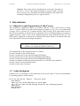
1
lektronik
abor
Laboratory on Digital and Mixed-Signal
Electronic Circuit Design
Getting Started with
DE2, DA2 and DS2 Boards
Prof. Dr. Martin J. W. Schubert
Electronics Laboratory
Regensburg University of Applied Sciences
Regensburg
M. Schubert
Getting Started with DE2 and DA2 Boards
Regensburg Univ. of Appl. Sciences
Abstract. The reader will be introduced into some basic functions of
the Altera / Terasic DE2 board and learns to operate simple A/D and
D/A converters on a self-made DA2 board designed by the author and
assembled at Regensburg Univ. of Appl. Sciences.
1 Introduction
1.1 Objectives and Organization of this Course
This document is intended to make you familiar with the Terasic's DE2 board [1] using
Altera's Cyclone II FPGA [2]. More documentation is found e.g. at [3]-[6]. It is assumed that
you have Altera’s Quartus II 8.1 software and the "DE2 System" CD or some other access to
the DE2 user manual [3] and the board’s schematics [4]. At OTH Regensburg, University of
Applied Sciences, such a copy can be obtained from the school internal network [5]. The
DE2-baord is employed to operate the self-made DA2 board, which is concerned with some
basic A/D and D/A conversion design techniques.
All material afforded and supporting jobs performed by
students were funded by student’s tuition fees.
The organization of this communication is as follows:
Section 2 introduces the DE2 hardware,
Section 3 teaches how to get started with the DE2 Board
Section 4 teaches how to get started with Daughter Board DA2
Section 5 teaches how to get started with Grandchild Board DS2
Section 6 assembles all that parts mentioned before to a ΔΣ ADC and a ΔΣ DAC.
Section 7 draws relevant conclusion and
Section 8 offers some references
1.2 Acknowledgment
I thank Terasic Technologies [1] for admission to use screen copies of Terasic documentation
for teaching purposes in this lectures.
At 19.09.2014 08:49, Terasic - Dong Liu wrote:
Dear Martin,
Thank you for using DE2 board to teach VHDL.
Yes, you can open all DE2 design resources for teaching purpose.
Thank you!
Best Regards,
Doreen liu
-2-
M. Schubert
Getting Started with DE2 and DA2 Boards
Regensburg Univ. of Appl. Sciences
2 Basic Understanding of the DE2 Board
This chapter can be done without the hardware. Have the Altera documentation available.
2.1 Document DE2_Introduction_box.pdf
Search for the string "Cyclone". Under point DE2 Board Features: Which FPGA is
employed?
............................................................
Under point Specifications → FPGA. What is the accurate name of the FPGA on the board?
............................................................
2.2 Document DE2_UserManual.pdf
Get an orientation: Look at the Contents and Read the headlines of the five chapters. See fig
2.1 of the User Manual (as copied below from [3]):
->>> ERROR: JP1=GPIO_0 and JP2=GPIO_1 are exchanged in Fig. 2.1 above!
Check the board on the image above: Where is the power-on switch, 9V DC Power in, USB
Blaster Port, Run/Prog switch, LCD display module, the 7-segment displays, the 18 red and 9
green LEDs, the 18 toggle switches and 4 push buttons, the Cyclone II FPGA and the
expansion headers JP1 and JP2, corresponding to GPIO_0 and GPIO_1, respectively? (On
the DE2-70 Board we have the GPIO_x names only.)
-3-
M. Schubert
Getting Started with DE2 and DA2 Boards
Regensburg Univ. of Appl. Sciences
2.2.1 Questions Related to the FPGA
How many phase-locked loops (PLLs) does the FPGA have?
............
How many multipliers with how many bits in / out does the FPGA have?
You’ll find the I/O bit widths in document → ..\Datasheets\Cyclone_II\cyc2_cii5v1_01.pdf on
the DE2-CD. You’ll find it in the internet or at OTHR in file CD_DE2_for_Quartus7.2.zip at
K:\SB\Hardware\Altera\DE2_Board_Altera-Cyclone2-EPC2C35\CD_DE2_for_Quartus7.2.
............................................................
The FPGA is connected with a Ball-Grid-Array (BGA). How many pins does it have? ....
Organized in how many row and columns? .................................
(You may find the answer later in the Quartus II software with Assignments → Pins after
correct settings of Assignments → Device...)
2.2.2 Questions Related to the LEDs and Switches
See chapter "Using the LEDs and Switches" in the User Manual and check signal names with
the definitions in file DE2_pin_assignments.csv on the DE2-CD [5].
What are the names of the signals connected to the 18 toggle switches ?
...........
What are the names of the signals connected to the 4 push buttons switches ? ...........
What are the names of the signals connected to the 18 red LEDs ?
...........
What are the names of the signals connected to the green LEDs ?
...........
Which level (High/Low) will turn a red LED on?
...........
Which level (High/Low) will turn a green LED on?
...........
2.2.3 Questions Related to the 7-Segment Displays
See chapter "Using the 7-Segment Displays" in the User Manual.
What are the names of the signals connected to the 7-segment displays ?
...............................................................
Which level (High/Low) will turn a LED of the 7-segment display on?
..........
7-seg.-LEDs with undriven input signals are ..... → Undriven signals are at state ......
-4-
M. Schubert
Getting Started with DE2 and DA2 Boards
2.2.4 Questions Related to the Expansion Headers
Cutout of DE2_schematics.pdf [4],
p.9. From left to right: Wire name,
chip-pin-name, intended purpose.
-5-
Regensburg Univ. of Appl. Sciences
M. Schubert
Getting Started with DE2 and DA2 Boards
Regensburg Univ. of Appl. Sciences
Fig. 4.10 from DE2 User Manual [3] shows an extraction of the schematic diagram. (For
complete schematics see file DE2_schematics.pdf [4].) The schematics is drawn in unreadable
parts. Complete the figure below to deliver a connectedly schematics for the circuitry from
the FPGA to Pins 1 and 3 of both, JP1 (=GPIO_0) and JP2 (=GPIO_1). Label all elements:
resistors incl. values, diodes, pins at the expansion headers and the FPGA, supply voltages,
wire names and their VHDL signal names as defined in the DE2_pin_assignments.csv file.
JP1 / GPIO_0
1
TopView–WireBond
Altera-Cyclone2, P2C35F672C6
JP2 / GPIO_1
1
Figure 2.2.4: protection circuitry between chip and GPIO expansion header pin.
-6-
M. Schubert
Getting Started with DE2 and DA2 Boards
Regensburg Univ. of Appl. Sciences
3 Getting started with the DE2 Board
3.1 Observe the Board
Check the DE2 board in your hands: Where is the power-on switch, 9V DC Power in, USB
Blaster Port, Run/Prog switch, LCD display module, the 7-segment displays, the 18 red and 9
green LEDs, the 18 toggle switches and 4 push buttons, the Cyclone II FPGA and the
expansion headers JP1 and JP2?
What is the labeling mistake in figure 2.1? Would be right? ......................
Find on the DE2 board all devices that you draw in the figure above (except the wires).
............................................................
3.2 VHDL Test File
Listing 3.2: VHDL test file
-- For Board: Altera DE2 with FPGA Cyclone II EP2C35F672C6
LIBRARY ieee; USE ieee.std_logic_1164.ALL,ieee.std_logic_signed.ALL;
ENTITY de2_test IS
PORT(CLOCK_50,CLOCK_27:IN std_logic;
key:IN std_logic_vector(3 DOWNTO 0); -- low when pressed
sw:IN std_logic_vector(17 DOWNTO 0); -- low when pulled down
ledg:BUFFER std_logic_vector(8 DOWNTO 0); -- high active
ledr:BUFFER std_logic_vector(17 DOWNTO 0); -- high active
hex0,hex1,hex2,hex3,hex4,hex5,hex6,hex7:OUT std_logic_vector(0 TO 6);
gpio_0:BUFFER std_logic_vector(35 DOWNTO 0);
gpio_1:INOUT std_logic_vector(35 DOWNTO 0)
);
END ENTITY de2_test;
ARCHITECTURE rtl_de2_test OF de2_test IS
TYPE t_7seg IS ARRAY(0 TO 15) OF std_logic_vector(0 TO 6);
CONSTANT c7seg:t_7seg:=("1111110", "0110000", "1101101", "1111001",
"0110011", "1011011", "1011111", "1110000", "1111111", "1110011",
"1110111", "0011111", "1001110", "0111101", "1001111", "1000111");
BEGIN
gpio_1(17 DOWNTO 0) <= sw;
ledr(17 DOWNTO 0) <= sw(17 DOWNTO 0);
ledg( 7 DOWNTO 4) <= key(3 DOWNTO 0);
ledg( 3 DOWNTO 0) <= key(3 DOWNTO 0);
ledg(8) <= sw(0);
p_check_hex:PROCESS(sw(0))
BEGIN
IF sw(0)='0' THEN
hex0<=c7seg(0); hex1<=c7seg(1); hex2<=c7seg(2); hex3<=c7seg(3);
hex4<=c7seg(4); hex5<=c7seg(5); hex6<=c7seg(6); hex7<=c7seg(7);
ELSE
hex0<=c7seg(8); hex1<=c7seg(9); hex2<=c7seg(10); hex3<=c7seg(11);
hex4<=c7seg(12); hex5<=c7seg(13); hex6<=c7seg(14); hex7<=c7seg(15);
END IF;
END PROCESS p_check_hex;
END ARCHITECTURE rtl_de2_test;
CONFIGURATION con_de2_test OF de2_test IS
FOR rtl_de2_test
END FOR;
END CONFIGURATION con_de2_test;
save: de2_test.vhd → de2_test_sol0.vhd
-7-
M. Schubert
Getting Started with DE2 and DA2 Boards
Regensburg Univ. of Appl. Sciences
3.3 Installing and Starting the Software
(Who needs much more detailed explanations than given in this subchapter is referred to file
tut_quartus_intro_vhdl.pdf (30 pages) within DE2-CD\DE2_tutorials\.)
First of all we need some preconditions:
Create a directory on your Windows operating system, let’s call it de2_test. (You may take
an other name.)
Create an ASCII file containing the VHDL code shown in listing 3.2, name it de2_test.vhd
and deposit in your directory de2_test.
Copy file DE2_pin_assignments.csv from DE2-CD\DE2_lab_exercises\ into your
directory de2_test.
Directory de2_test should now contain 2 files: de2_test.vhd and DE2_pin_assignments.csv.
Install Quartus II on your computer. Within Regensburg University of Applied Sciences
(HS.R) your can start Quartus II 8.1 from Windows Start menu:
Start → Programme → Fachbereiche → Elektrotechnik → Altera → Quartus II 8.1.
Select menu point Create a New Project (New PROJECT Wizard) → Next →
Directory: “…\de2_test”
Name of the Project: de2_test
Top-level entity: de2_test → Finish
Quartus II: Project → Add/Remove Files in Project → Add All (adds de2_test.vhd) → ok
Quartus II: Assignments → Device → Family: Cyclone II, Device EP2C35F672C6 → ok
Quartus II: Assignments → Import Assignments → … → DE2_pin_assignments.csv -> ok
Quartus II: Processing → Start Compilation (exists also as short-cut button in the top bar)
After some time you should see: "Full Compilation was successful (390 warnings"). Look
what the synthesizer made of your VHDL code:
Quartus II: Tools -> Netlist -> RTL Viewer
-8-
M. Schubert
Getting Started with DE2 and DA2 Boards
Regensburg Univ. of Appl. Sciences
3.4 Installing and Operating the Hardware
(Who needs much more detailed explanations than given in this subchapter is referred to file
tut_initialDE2.pdf (6 pages) within DE2-CD\DE2_tutorials\.)
Connect the power cable and switch the board ON. LCD module, 7-segment displays and all
diodes should have some activity now due to a start-up procedure.
Set the Run/Prog-Switch on Run, connect the USB-Blaster Port of the Board to an USB slot
of your computer. The New Hardware Wizard appears.
To install the USB-Blaster for a stand-alone computer follow the instructions of
tut_initialDE2.pdf. (You have to install the usb_blaster by leading the system to path
<Quartus_insatallation_directory>\quartus\drivers\usb-blaster.)
On the HSR network the USB-Blaster is pre-installed. After connection of the DE2 board
select Software automatisch installieren → USB-Blaster → Fertigstellen.
Quartus II: Tools → Programmer →Hardware Setup → USB-Blaster [USB-0].
Within the Programmer you should now see the file de2_test.sof in a line with checkbox
Program / Configure activated. The switch left to the 7-segment displays is set to RUN.
Quartus II Programmer: Start.
Blue LED LOAD on the DE2 board should turn on for a while and then the blue LED GOOD.
Congratulations! You got it! Your board is ready to be tested now!
There are many files in the de2_test directory. Save those with extensions *.vhd, *.qpf and
*.qsf. After compilation the file with extension *.sof is the binary file to program the FPGA.
In case of interest recover the rest of the files:
After deleting anything in this directory except de2_test.vhd, de2_test.qpf and de2_test.qsf
double-click left mouse button on de2_test.qpf. Quartus II comes up. Select Tools →
Compile and Programmer to regenerate the deleted files.
-9-
M. Schubert
Getting Started with DE2 and DA2 Boards
Regensburg Univ. of Appl. Sciences
3.5 Testing Soft- and Hardware
After downloading file de2_test.sof into the FPGA we begin to check its functionality and
understand the VHDL code lines defining it. The statements
ledr(17 DOWNTO 0) <= sw(17 DOWNTO 0);
ledg( 7 DOWNTO 4) <= key(3 DOWNTO 0);
ledg( 3 DOWNTO 0) <= key(3 DOWNTO 0);
allow to switch all red LEDs an and off using the toggle switches SW0…SW17 below the
respective LEDs LEDR0…LEDR17. Try it! Does it work?
Pushbuttons KEY0…KEY3 should allow to switch off the green LEDs LEDG0…LEDG3.
When pushing KEY# (# = 0…3), then signal key(#) goes to state
...............
Not only LEDs are driven by the switches, also 18 pins of the expansion header JP2
(=GPIO_1) by line
gpio_1(17 DOWNTO 0) <= sw;
Which expansion header pin is driven by toggle switch SW0?
.....................
The 7-segment displays should show their index if SW0='0' or index+8 if SW0='1'. This is
caused by the code lines
IF sw(0)='0' THEN
hex0<=c7seg(0); hex1<=c7seg(1); hex2<=c7seg(2); hex3<=c7seg(3);
hex4<=c7seg(4); hex5<=c7seg(5); hex6<=c7seg(6); hex7<=c7seg(7);
ELSE
hex0<=c7seg(8); hex1<=c7seg(9); hex2<=c7seg(10); hex3<=c7seg(11);
hex4<=c7seg(12); hex5<=c7seg(13); hex6<=c7seg(14); hex7<=c7seg(15);
END IF;
But something is wrong with the hex-displays! What? Repair it using operator NOT for bitvectors! (e.g. not_vector <= NOT vector;)
save: de2_test.vhd → de2_test_sol1.vhd
- 10 -
M. Schubert
Getting Started with DE2 and DA2 Boards
Regensburg Univ. of Appl. Sciences
4 Getting Started with Daughter Board DA2
4.1 The DA2 Daughter-Board Hardware
DAC1
DAC1out
R
2R
R
2R
A4
A1
A6
R
2R
R
2R
R
2R
2R
DAC1out_b
DAC1out_b
A7 A8
A2
C1=1 nF
R
2R
MAX4234
A5
R
2R
VCC5
n1
OA1
R=10K
= DE2 / JPx-pin(10:4,2), x=1,2
DAC1(7:0) = gpio(9:3,1)
2R
A3
line_out (green)
A9
TRS out Right
A10
TRS out Left
2 x 100F
aluminum
electrolyt
DAC2
n2
A15
A16
A17
A14
VCC5
MAX4234
Rx
Rx
Rx
Rx
Rx
DAC2out_b
A11 A12
A18
VCC5
Rx
Rx
DAC2out_b
OA2
A13
Rx
C2=10 nF
B5
B6
20K
20K
Diff_ref_b
Diff_in_P
Rx=8K
OA5
4
20K
R48
B3
gnd
MAX4232 OA6
DAC3
B1
MAX4232
B2
B7 B8
Diff_in_M
Rx=8K
DiffOut
20K
20K
Rx
Rx
DAC3out
Rx
A23
Rx
A25
Rx
VCC5
A24
n3
MAX4234
A22
DAC3out_b
DAC3out_b
OA3
A21
A19 A20
Rx
Rx
A26
A27
100nF
line_in (blue)
TRS_in_Left
A34
TRS connector
A32
A29
TRS_in_Left_C
1F
A36 A35 A37
gnd VCC5
20K
R1
n4
A40
n7
A30
VCC5
2K
n5
OA4
A39
R9
MAX4234
20K
4.7F
Fig. 4.1-1: Schematics of the DA2 daughter board
- 11 -
R19
n6
LT1712 VCC33
CP7
VCC33
2K
C3
C5
100nF
C7
C9
LT1712 VCC33
VCC33
A33 A31
C1
C2
C11
C13
C15
C16
2K
CP0
100nF
ADC(7:0) = gpio(35:28)
A31
A38
TRS_in_Right
CP_in_P
A28
= DE2 / JPx-pin(40:33), x=1,2
C3=10 nF
= DE2 / JPx-pin(32,31:28:23), x=1,2
DAC3(7:0) = gpio(27:20)
Rx
VCC5
Diff_ref
VCC5
CPerf# (#=0...7)
= DE2 / JPx-pin(22,20,18:13), x=1,2
DAC2(7:0) = gpio(19,17,15:10)
DAC2out
TRS connector
M. Schubert
Getting Started with DE2 and DA2 Boards
Connector
0
1
2
3
4
5
6
7
2
1
4
3
6
C
8
7
9
12
11
14
13
16
15
Connector
0
DAC1out
1
1 nF
2
5
10
Regensburg Univ. of Appl. Sciences
3
4
TRS out Right
5
6
7
CP ref (7 : 0)
10 nF
CP out (7:0)
DAC2out
DAC3out_b
Connector
GND
1
2
3
4
5
6
7
8
9
10
11
12
13
14
15
Connector
Diff Out
8
7
Diff in P
6
5
Diff Ref
4
3
Diff In M
2
1
10 nF
DAC3out
100nF
n6
16
1
2
3
4
5
6
A
n1
7
8
DAC1out_b
9
10
TRS out Left
11
12
DAC2out_b
13
14
15
16
17
18
19
20
21
22
23
24
25
26
27
28
29
31
30
32
CP in P
33
34
TRS_in_Left
n2
DAC3out_b
n3
35
36
TRS_in_Left_C
n4
37
38
TRS_in_Right
n5
39
40
n7
B
Pins 1, 3, 19, 21 of GPIO-Header:
Diff Ref b
1
19
3
21
Fig. 4.1-2: Connectors of the DA2 daughter board
Fig. 4.1-1 shows the DA2 daughter board schematics.
Fig. 4.1-2 illustrates the DA2 board from the Santa-Cruz connector point of view.
Fig. 4.1-3(a) is related to the user header of the DE2 board and maps the GPIO labels
to the Santa-Cruz connector pins.
Fig. 4.1-3(b) is related to the user header of the DE2-70 board and maps the GPIO
labels to the Santa-Cruz connector pins.
This tutorial is made for the DE2 board, but the user-header pins are assigned such, that
compatibility to the DE2-70 board is supported. Therefore pins 1, 3, 19, 21 of the user header
remain unused. They are made available on the DE2 daughter board. DE2-board users can
employ them arbitrarily. DE2-70-board users can observe the PLL behavior with these pins.
- 12 -
M. Schubert
Getting Started with DE2 and DA2 Boards
(a) User header of DE2 board
Regensburg Univ. of Appl. Sciences
(a) User header of DE2-70 board
Fig. 4.1-3: User header configurations of DE2 and DE2-70 boards, copied from the
respective user manuals.
- 13 -
M. Schubert
Getting Started with DE2 and DA2 Boards
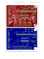
Fig. 4.1-4: DA2 board schematics (by Markus Buchhart, 2010)
- 14 -
Regensburg Univ. of Appl. Sciences
M. Schubert
Getting Started with DE2 and DA2 Boards
Regensburg Univ. of Appl. Sciences
Fig. 4.1-5: DA2 board (top) top and (bottom) bottom layer layout (by M. Buchhart, 2010)
- 15 -
M. Schubert
Getting Started with DE2 and DA2 Boards
Regensburg Univ. of Appl. Sciences
4.2 Digital-to-Analog Converters (DACs)
4.2.1 Flash-DAC Theory
(b)
(a)
0
1
2
3
4
5
6
7
8
U0
G0
U1
G1
U2
G2
U3
G3
U4
G4
U5
G5
U6
G6
U7
G7
(c)
Gsum
DAC#out
Usrc
DAC#out,
#=2,3
Figure 4.2.1: (a) A 9-level thermometric code, (b) Flash DAC and (c) its equivalent model
7
1
In the figure above we have Z out
Gsum G j
and
U src
j 0
7
Gj
GsumU j .
j 0
DAC2 and DAC3 in Fig. 4.1-1 deliver 9-level output from 8-bit thermometric code to pins
labeled DAC2out and DAC3out, respectively. What is their output resistance for ideal voltage
sources and 8K-resistors?
...........................................
Compute UDAC#out9 = f(L,VCC) with L input voltages being at VCC and the others at GND=0V?
Rj=8K for j=0...8. Label the 9 voltage levels in the figure below for VCC=VCC33=3.3V.
Figure 4.2.2:
Minimum DAC output step:
DA =
3.3 V
.......................
L=9 level DAC output voltage formula:
UDAC#out =
.....................
with #=2,3. Amplification:
ADA =
0
0
........................
- 16 -
1
2
3
4
5
6
7
8
L
M. Schubert
Getting Started with DE2 and DA2 Boards
Regensburg Univ. of Appl. Sciences
These 8-bit/9-level DAC with thermometric code seems to be not very efficient as 8 bits
could be translated into 256 levels. However, combined with oversampling techniques such as
dynamic element matching (DEM) and delta-sigma (ΔΣ) modulation this kind of DAC can
represent an arbitrary number of levels with incredible accuracy.
4.2.2 R2R-DAC Theory
Uout
R
Fig. 4.2.2:
R2R DAC
R
R
R
R
R
R
2R
2R
2R
2R
2R
2R
2R
2R
2R
'0'
a0
a1
a2
a3
a4
a5
a6
a7
The R2R ladder DAC with output DAC1out delivers an output voltage of
7
U DAC1out U j 2 j 8
j 0
with Uj being VCC33=3.3V or GND=0V as can be seen e.g. from script A/D/A Converters [7]
or Schaltungstechnik [8]. The output impedance of the R2R-DAC in Fig. 4.1-1 is R.
For measurement & test applications the inaccuracy of the most significant bit (MSB) must be
less than or equal to the half of the least significant bit (LSB). For 1% resistors this would be
6 bits, corresponding to an impact of 2-6=1/641.56%. In other situations, e.g. processing
acoustic signals, this holds true for the most significant used bit. Quiet passages of music may
use only some LSBs.
4.2.3 Connecting the DA2 Daughter Board
Remove all jumpers from grandchild board DS2 attached below daughterboard DA2.
Connect the DA2 daughter board to the JP2 = GPIO_1 expansion header of the DE2 board.
Thus it will be controlled by signals gpio_1(35…0).
Within your Windows operating system do the following:
Copy directory de2_test generated within the previous chapter and rename it to de2_dac.
Delete all files within directory de2_dac with exception of de2_test.vhd.
Rename the last version of de2_test.vhd to de2_dac.vhd.
Open de2_dac.vhd and rename all strings "de2_test" to "de2_dac".
Restart Quartus II and create within directory de2_dac a new project named de2_dac.
(FPGA is still Cyclone II – EP2C35F672C6, and do not forget to import pin-assignments
from file DE2_pin_assignments.csv.)
Compile de2_dac.vhd and download de2_dac.sof to your DE2 board.
At this point the board should do exactly the same as it did for project de2_test in the
previous chapter. Does it?
save: de2_dac.vhd → de2_adc_dac_sol0.vhd
- 17 -
M. Schubert
Getting Started with DE2 and DA2 Boards
Regensburg Univ. of Appl. Sciences
4.2.4 Driving the DACs
Copy all 36 signals of gpio_1 to gpio_0 for monitoring reasons (, as we cannot directly
measure the pins of gpio_1 covered by the 40-pin-connector). To do so include the following
code line somewhere in the concurrent code:
-- copy gpio_1 to gpio_0 for monitoring reasons
gpio_0 <= gpio_1;
Include the code lines below somewhere in the concurrent code of the architecture:
SIGNAL dac1dout256,dac2dout9,dac3dout9:std_logic_vector(7
...
-- set drivers to the 3 DACs
dac1dout256 <= sw(7 DOWNTO 0); -- input to 256-level DAC
dac2dout9
<= sw(7 DOWNTO 0); -- input to
9-level DAC
dac3dout9
<= sw(7 DOWNTO 0); -- input to
9-level DAC
DOWNTO 0);
1
2
3
We avoid to use pins 1, 3, 19, 21 of the user headers for reasons of compatibility with the
DE2-70 board’s user header, because the DE2-70 assigns these pins to a PLL as shown in Fig.
4.1-3(b). Consequently, working with the top-level entity de2_test we avoid using signals
gpio_x(.......) , gpio_x(.......) , gpio_x(.......) , gpio_x(.......)
Attach daughter-board DA2 to the 40-pin connector JP2 (=GPIO_1) of the DE2-board.
Modify other drivers to signal gpio_1(...) such, that:
signal dac1dout256 controls the output voltage of the analog signal DAC1out on DA2 board,
signal dac2dout9 controls the output voltage of the analog signal DAC2out on DA2 board,
signal dac3dout9 controls the output voltage of the analog signal DAC3out on DA2 board.
To do so replace line
gpio_1(17 DOWNTO 0) <= sw;
by the following statements, compile the new code and download into the FPGA:
-- drive DAC1:
gpio_1( 9 DOWNTO
gpio_1( 1)
3) <= dac1dout256(....................);
<= dac1dout256(....................);
-- drive DAC2:
gpio_1(19)
<= dac2dout9(....................);
gpio_1(17)
<= dac2dout9(....................);
gpio_1(15 DOWNTO 10) <= dac2dout9(....................);
-- drive DAC3:
gpio_1(....................) <= dac3dout9;
save: de2_adc_dac.vhd → de2_adc_dac_sol1.vhd
- 18 -
M. Schubert
Getting Started with DE2 and DA2 Boards
Regensburg Univ. of Appl. Sciences
4.2.5 Testing DAC1
sw(7:0)
Fig. 4.2.5: Test setup for DAC1.
A1
Zout1
A3
A6
DAC1out
Usrc1
multimeter
4.2.5.1 Measuring the Equivalent Inner Source Voltage Usrc1
Connect a voltmeter to output of DAC1, which is drawn as source voltage and output
impedance in Fig. 4.2.5. As the voltmeter has a high input impedance, we measure DAC1’s
equivalent source voltage Usrc1. Use switches sw0 ... sw7 for the following questions:
VDD theoretically: 3.3V, (available e.g. at pin 29 of GPIO 1,2) , measured ...........
Usrc1 for DAC1 varies in ......... steps from a minimum voltage of ..........V
to a theoretical max. voltage of ..........................
, measured .........
The resolution is theoretically: ..........................
, measured .........
Look into the data sheet of the max423x operational amplifier:
Common mode input voltage range:
..................................,
Typical output voltage swing at RL=200:
...................................,
Input bias current:
..................................,
Input offset voltage:
typical:
............. max: ................
On DA2 board: Set jumper A3-A4. Does buffer OA1 drive DAC1out_b? ................
Input offset voltage of amplifier OA1 (measure e.g. between pins A1–A7)? .............
4.2.5.2 Measuring the Equivalent Output Impedance Zout1
Expected output impedance from Fig. 4.1-1:
Zout1,ideal = ...................
Method A:
Set any voltage Usrc1>0V (e.g. VDD/2=1.65V), measure it:
Usrc1 = .........
Switch from voltmeter to ampere-meter and measure the output current: Iout1 = ..........
The output impedance is Zout1 = Usrc1 / Iout1 = ................
Method B:
Set voltage Usrc1=0V and measure with an Ohm-meter versus ground: Zout1 = .............
- 19 -
M. Schubert
Getting Started with DE2 and DA2 Boards
4.2.6 Testing DAC2
Regensburg Univ. of Appl. Sciences
OA2 o.k.? ... , Offset voltage: ............
sw(7:0)
Fig. 4.2.6: Test setup for DAC2.
A14
Zout2
A15
A17
DAC2out
Usrc2
multimeter
4.2.6.1 Measuring the Equivalent Inner Source Voltage Usrc2
Use switches sw0 ... sw7 for the following questions:
Usrc2 for DAC2 varies in ......... steps from a minimum voltage of ..........V
to a theoretical max. voltage of
.......................... , measured ..........
The resolution is theoretically:
.......................... , measured ..........
4.2.6.2 Measuring the Equivalent Output Impedance Zout2
Expected output impedance from Fig. 4.1-1:
Zout2,ideal = ...................
Method A:
Set any voltage Usrc1>0V (e.g. VDD/2=1.65V), measure it:
Usrc2 = ..........
Switch from voltmeter to ampere-meter and measure the output current: Iout2 = ...........
The output impedance is Zout2 = Usrc2 / Iout2 = ..............
Method B:
Set voltage Usrc2=0V and measure with an Ohm-meter versus ground: Zout2 = .............
4.2.7 Testing DAC3
OA3 o.k.? .... , Offset voltage: ............
4.2.7.1 Measuring the Equivalent Inner Source Voltage Usrc3
Remove DS2 grandchild board under this DA2 board or remove jumper E1-E3 on it (→ see
Fig. 5.1.1). Use switches sw0 ... sw7 for the following questions:
Usrc3 for DAC3 varies in ......... steps from a minimum voltage of ..........V
to a theoretical max. voltage of
.......................... , measured ..........
The resolution is theoretically:
.......................... , measured ..........
4.2.7.2 Measuring the Equivalent Output Impedance Zout3
Expected output impedance from Fig. 4.1-1:
Zout3,ideal = ...................
The measured output impedance is Zout3 = ....................
- 20 -
M. Schubert
Getting Started with DE2 and DA2 Boards
Regensburg Univ. of Appl. Sciences
4.3 Analog-to-Digital Converter (ADC)
Within your Windows operating system do the following:
Copy directory de2_dac generated within the previous chapter and rename it to
de2_adc_flash.
Delete all files within directory de2_adc_flash with exception of de2_dac.vhd.
Rename de2_dac.vhd to de2_adc_flash.vhd.
Open de2_adc_flash.vhd and rename all strings "de2_dac" to "de2_adc_flash".
Restart Quartus II and create within directory de2_adc_flash a new project de2_adc_flash.
Compile de2_adc_flash.vhd and download de2_adc_flash.sof to your DE2 board.
At this point the board should do exactly the same as it did for project de2_dac in the
previous chapter. Does it?
save: de2_adc_flash.vhd → de2_adc_flash_sol0.vhd
4.3.1 Trimming the Flash-ADC
The 8 threshold voltages are labeled on the board with CPref0,...,CPref7 (test points C2, C4,
... C16). Compute the 8 thresholds in Fig. 4.3.1(b) and turn the 8 potis to the computed values.
CPref0 gets the lowest threshold, increasing with index Cpref7 gets the highest threshold.
The positive 8 comparators inputs the are connected and labeled CP_in_P having several test
points. Ideally, the Flash-ADC would have an infinite impedance and zero input current.
However, most comparators have input bias currents.
Look into the LT1712 data sheet. What is its typical input bias current?
...........
What is the typical input bias current of the total Flash-ADC? ...................
- 21 -
M. Schubert
Fig. 4.3.1(a):
Basic principle of a
flash ADC. The m:n
decoder logic can be
realized as simple
summation of the
comparator’s output
bits.
Getting Started with DE2 and DA2 Boards
UADCin
Regensburg Univ. of Appl. Sciences
Uref
R
2
L-1
VT,L-1
R
2
VT,2
DADCout,M-1
DADCout,1
DADCout,0
L:M
3
VT,3
Logic Decoder
R
R
1
VT,1
R
2
Write the formula VT,i=f(i=0...7,VCC) for the 8 required threshold voltages of the comparators
delivering the 8-bit decision into Fig. 4.3.1. Write the VT,i to the right side of the figure.
Figure 4.3.1(b):
Remember: L=9 level DAC
output voltage formula:
UDACout
VT,x
3.3
2.8875
UDAC#out = i·DA, i=0...L-1
Find: L=9 level DAC input
threshold formula using
Uref=VCC=3.3V, i=0...L-1.
VT,i = ...............
with AD = ...........
Amplification:
AAD = ...............
2.475
2.0625
1.65
1.2375
0.825
0.4125
0
0
1
- 22 -
2
3
UADCin /
7
8
L
M. Schubert
Getting Started with DE2 and DA2 Boards
Regensburg Univ. of Appl. Sciences
4.3.2 Using DAC3out as Voltage Source
DAC3out9
sw(7:0)
CP_in_P
A27
Zout3
A22 A23 A25
A28
Flash
ADC
A31
Usrc3
A32
=VDD/2
C2
C4
C6
...
C16
8
adc_in(7:0)
1
(9-Level)
A31
Figure 4.3.2: Using DAC3out as Voltage Source
Set U(DAC3out) to VDD/2, using for example sw(7…0)="00001111", and measure the
voltage at test point A25. Write U(DAC3out) in box "unconnected" in Tab. 4.3.2.
Connect U(DAC3out) to the Flash-ADC’s input CP_in_P (that must not have other
connections) by shorting pins A25 and A27. Write U(DAC3out) in box
"DAC3out=CP_in_P " of table 4.3.2.
Table 4.3.2: Impact of comparator’s input bias currents on output impedance of DAC3.
DAC3out:
U(DAC3out):
unconnected
DAC3out=CP_in_P
Difference
How do you explain the voltage jump when pins A25 and A27 shorted?
.........................................................................
.........................................................................
Read the comparator’s outputs to the FPGA.
Declare SIGNAL adc_din:std_logic_vector(7 DownTo 0)
and include the statement
adc_din <= gpio_1(....................);
Monitor the ADC’s output using the green LEDs by modifying (other drivers must be
removed!) their driver to
ledg(7 DOWNTO 0) <= adc_din;
-- output to the green diodes
save: de2_adc_flash.vhd → de2_adc_flash_sol1.vhd
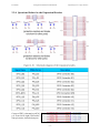
Table 4.3 lists the actual assignments of switches, LEDs and gpio signals.
Measure the voltage DAC3out and observe the green diodes. What correlation do you observe
between the number of switches sw(7...0) driving logical HIGH state and the number of green
LEDs turned on?
.........................................................................
- 23 -
M. Schubert
Getting Started with DE2 and DA2 Boards
Regensburg Univ. of Appl. Sciences
Table 4.3: Usage of the gpio_#(i) headers, (#=0,1), the ADC’s input and the switches sw(j).
gpio-index i
35 : 28
27 : 20
19
18
17
16
15 : 10
9 : 3
2
1
0
mode
IN
OUT
OUT
OUT
OUT
OUT
OUT
-
Usage of signal gpio_1(i)
adc_din(7:0)
dac3dout9(7:0)
dac2dout9(7)
always unused
dac2dout9(6)
always unused
dac2dout9(5:0)
dac1dout256(7:1)
always unused
dac1dout256(0)
always unused
Other signal
usage of other signal
adc_din(7:0) driving ledg(7:0)
sw(17:0)
driving ledr(17:0)
sw( 7:0)
driving DACs(7:0)
4.3.3 Using the PC’s Sound Card as Signal Source
A38
TRS_in_Right
CP_in_P
A27
line_in (blue)
A28
TRS_in_Left_C
n4
TRS_in_Left
A34
TRS connector
A35 A37
VCC5
1F
A40
n7
A32
n6
A33
C2
C4
C6
...
C16
8
adc_in(7:0)
1
(9-Level)
A31
OA4
gnd VCC5
20K
R1
A31
2K
n5
A36
Flash
ADC
A39
R9
MAX4234
R19
20K
4.7F
(a) Top: Circuit assembled
on DA2 board.
(b) Right: PC screen shot:
Settings of Timo Esser’s
Test Tone Generator [9],
[10] driving the PC
soundcard: 1000Hz
sinusoidal, Amplitude:
-21dBFS.
Figure 4.3.3: Using the sound
card as signal source.
Of course, you can use
other signal sources also!
Goal of this subchapter is to assemble the circuit in Fig. 4.3.3(a), quantize a sinusoidal test
tone with the Flash-ADC and get the upper two curves of Fig. 4.3.4(b) on the oscilloscope.
- 24 -
M. Schubert
Getting Started with DE2 and DA2 Boards
Regensburg Univ. of Appl. Sciences
A. Program DE2 board with VHDL Source Code:
To output the information of the 9-level Flash-DAC immediately via DAC2 and DAC3,
replace the code lines
dac2dout9 <= sw(7 DOWNTO 0); -- input to 9-level DAC 2
dac3dout9 <= sw(7 DOWNTO 0); -- input to 9-level DAC 3
with
dac2dout9
dac3dout9
<= adc_din
<= adc_din
save: de2_adc_flash.vhd → de2_adc_flash_sol2.vhd
into the actual VHDL code, compile with Quartus II and download it into the Cyclone II
FPGA on the DE2 board.
Connect CH2 of your oscilloscope with DAC3out (e.g. test point A25). This curves
corresponds to the blue staircase line in Fig. 4.3.4(b).
B. Circuit Assembly acc. To Fig. 4.3.3(a) on the DA2 daughter board:
Hint: TRS = Tipp-Ring-Sleeve connectors are the ones typically used for speakers.
1.
2.
3.
4.
5.
6.
7.
8.
Remove jumper A25–A27 to disconnect DAC3out from CP_in_P.
Use -meter (between test points A33-A39) to adjust R19 to 1 K.
Shorten (jumper) test points A31-A33 to drive CP_in_P with OpAmp OA4 through R19.
Shorten (jumper) test points A35-A37 to drive OpAmp OA4’s IN+ with the soundcard.
Use poti R1 to set CP_in_P to a DC bias voltage of VDD/2=1,65V.
Drive a sinusoidal signal of ca. 250 mVpp to TRS_in_left. (For Test Tone Generation see C.)
Connect your oscilloscope’s CH1 to CP_in_P (A27) and CH4 to TRS_in_Left_C (A36).
Use poti R9 to adjust the amplification of OA4 to a factor 10 or 20dB. (See D.)
C. Test Tone Generation:
Prefer available Hardware to generate a test tone. If not available you can use your sound
card. Software is free available in the internet, e.g. Test Tone Generator [9].
(a) After a quick installation you will see the window shown in Fig. 4.3.3(b).
(b) Set the tone duration to 9999s, a sinusoidal 1000Hz tone and some –21dBFS to get a
peak-to-peak output amplitude of ca 250 mVpp. Click the ON button.
(c) Connect your PC’s soundcard output (green) with the DA2 boards TRS line_in jack.
D. With the Oscilloscope:
I. Oscilloscope: CH1 has 500mV/dev and CH4 has 50mV/dev.
II. According to point B.7 above CH1 has to show the 10 x amplified signal of CH4.
III. Use poti R9 to adjust the curves at CH1 and CH4 to the same amplitude.
IV. U(CP_in_P) shown at oscillator channel CH1 corresponds to the yellow sinusoidal curve
of the screen-shot in Fig. 4.3.4(b).
V. You should now have the sinusoidal (yellow) and staircase (blue) curves shown in Fig.
4.3.4(b) on your oscilloscope. You may slightly adapt the amplitude of the Test Tone
Generator to make the 9-level staircase curve as "nice" as shown in the Figure.
If the sinusoidal tone works well, drive on DA2 board DAC3out and additionally DAC2out
via the buffer amplifier AO2 to DAC2out_b and connect this to TRS out Left. Plug a speaker
to the DA2 board’s TRS line_out jack. Do you hear the test tone? .........
Disconnect the Test Tone Generator and play some music. Sound quality? .........
8 levels correspond to 3 bits. Our 9 levels correspond to ld(9) = ln(9)/ln(2) = ......... bits.
- 25 -
M. Schubert
Getting Started with DE2 and DA2 Boards
Regensburg Univ. of Appl. Sciences
4.3.4 Measuring the Quantization Noise
Osci
CH 1
Diff_in_P
20K
VCC5
20K
Diff_ref_b
CP_in_P
A27
A28 ...
OA5
B5
B6
Osci
CH 2
4
VCC5
20K
R48
Diff_ref
B3
VCC5
MAX4232 OA6
gnd
MAX4232
B7 B8
DAC3out_b
A19
A20
DiffOut
20K
Diff_in_M
B1
B2
Osci
CH 3
20K
(a) Top: Circuit assembled on DA2
board.
(b) Right: Oscilloscope screen shot:
(i) yellow + sinus.: CP_in_P,
(ii) blue in 9 levels: DAC3out,
(iii) green, bottom: Difference
=quantization noise: U(B7,B3).
Figure 4.3.4: Measuring quantization noise
Goal of this subchapter is to make the difference (= quantization noise) between sinusoidal
input and staircase output curve visible as shown in the bottom (green) curve of Fig. 4.3.4(b).
We should already have the sinusoidal (yellow) and staircase (blue) curves of Fig. 4.3.4(b) on
the scope. The last unit untested so far on the DA2 board is the differential amplifier, which is
well known in the literature as so-called instrumentation amplifier. It translates a differential
input voltage into an output voltage measured versus a user-defined reference :
Uq = U(DiffOut) - U(Diff_ref_b) = U(Diff_in_P) – U(Diff_in_M)
If available use the math menu of your oscil. to generate x-y. Otherwise do it with hardware:
Adjust poti R48 such that U(Diff_ref_b)=VDD/2=1.65V.
Connect CP_in_P to Diff_in_P and DAC3out_b to Diff_in_M.
Display U(DiffOut) on the oscilloscope as shown with the bottom (green) curve in
Fig. 4.3.4(b).
Note: To get the 1.65V DC biasing voltage out of the quantization noise measurement you have to either use
the AC feed-in mode on the scope (see figure) or to measure between points DiffOut and Diff_ref_b.
Assuming a triangular quantization noise voltage Uq(t) its effective (=rms) value computes to
/ 12 with =VDD / 8 in this case. Compute Uq,rms mathematically and measure it:
Mathematically: ..............................
- 26 -
Measured ..........
M. Schubert
Getting Started with DE2 and DA2 Boards
Regensburg Univ. of Appl. Sciences
5 Getting Started with Grandchild Board DS2
5.1 The DS2 Grandchild-Board Hardware
(a) DS2-Board Schematics: analog system or modulator, configurable of 1st and 2nd order
OA2
to DA2, A31
max4234
UB
1st
order
OA
s2
1
s3
E1
E9
s1 IN2
VCC
R2
OUT2
159pF
s
4
E11
IN1
UB
E8
OA
max4234
Rd
Rb
OA
11
s3
A25, from DA2
OUT2
10
4
6
7
8
9
JP2
11
5
JP3
IN1
7
8
3
9
JP2
JP2
10
Uin
2
1
s2
6
JP3
gnd
s5 s6
5
4
configured to digital mode and
2nd order modulator
JP1
3
Vcc
s1
2
1
s4
7
8
9
OUT2
s3
JP1
JP3
UB
6
3
(d) Connector E
analog mode and
1st order system
A25, from DA2
5
4
E6
max4234
(c) Connector E
2
JP1
3
E5
Ra
external
connctions
1
E4
100K
(b) Connector E
s2
E3
OUT1
159pF
4
100K
s5, s6
JP1
Uout
71K
UB
gnd
to DA2, A31
R1
C1
Rb1
JP3
100K
E10
Rb2
100K
100K Rc
E7
100K
JP2
E2
Ufb,in
Uin
2nd
order
C2
to DA2, A31
100K
A25, from DA2
A33, from DA2
max4234
UB
10
11
Fig. 5.1.1: (1) DS2-Board Schematics, cutoff frequency is fg=10KHz.
The DS2 grandchild board is plugged under the DS2 daughter board in the plug-line near the
DA2 board. The upper plug-line is intended for disconnected parking the DS2 board.
- 27 -
M. Schubert
Getting Started with DE2 and DA2 Boards
Fig 5.1.2: Eagle schematics
Fig 5.1.3: Eagle Layout: (a) Top view,
(b) Bottom view
- 28 -
Regensburg Univ. of Appl. Sciences
M. Schubert
Getting Started with DE2 and DA2 Boards
Regensburg Univ. of Appl. Sciences
5.2 Testing the DS2 Analog Board in a Stand-Alone Mode
We now want to operate the DS2 board as stand-alone 1st or 2nd order analog system with
lowpass characteristics.
The DS2 board gets its input signal from pin A33 which is wired to E10 of the DS2 board.
This connection is sketches as green wire W1 in Fig. 5.3. Wires W2 and W3 remain
disconnected in this subsection.
Connect pins E3-E4 with a jumper, but do not connect them to E1 and E2 to avoid driving
into the DA2 board. (→ The green wire W1 in Fig. 5.3 is connected, but wires W2 and W3 are
removed!) A 1st order system is obtained by connecting E10-E9, and a 2nd order system is
obtained by connecting E10-E11.
Sketch in Fg. 5.1.1(c) the settings of the jumpers to obtain a 1st order analog system.
Realize these settings with jumpers on the DS2 board.
We want to feed a 2Vpp sinusoidal Signal into the DS2 board’s Uin. To do so, we feed
200mVpp into the DA2-board’s Pin A34 or TRS connector, bridge A35-A37 and adjust
poti R9 such, that OA4 delivers an amplification of 10. → Measure 2Vpp at A33.
Cutoff frequency of this analog lowpass is 10KHz. Measure the output signal at pin E5 or
E6 for fin = 1KHz, 10KHz and 100KHz. What amplifications do you observe?
1st order: 1KHz: A = ..... dB,
10kHz: A = ..... dB,
100kHz: A = ..... dB,
Modify a single Jumper such, that we have a 2nd order analog system. Feed Uin as
detailed above and measure amplifications at pin E5 or E6:
2nd order: 1KHz: A = ..... dB, 10kHz: A = ..... dB, 100kHz: A = ..... dB,
- 29 -
M. Schubert
Getting Started with DE2 and DA2 Boards
Regensburg Univ. of Appl. Sciences
5.3 Testing the DS2 Board with Connections Via the DA2 Board
Fig. 5.3: Schematics and jumper situation
Remove jumper E3-E4. Replace it by jumper A25-A27 on the DA2 board. (In this mode
output amplifier OA1 of the DS2 board simply overrides the 1KΩ-output impedance of DAC3,
as we cannot disconnect DAC3.)
Sketch in Fg. 5.1.1(d) how to obtain an analog 2nd order system with Uout and Ufb,in of the
DS2 board connected with jumper A25-A27 on DA2 board.
Realize these jumper settings:
To connect the wire W2 to Uout of DS2 board set jumper E1-E3 on the DS2 board.
To connect the wire W3 to Ufb,in of DS2 board set jumper E2-E4 on the DS2 board.
To connect the DS2 board’s Uout with its Ufb,in set jumper A25-A27 on the DA2 board.
Experimental verification: We should get the same results as in the subchapter before:
Feed a 300mVpp-Signal into the DS2 board’s Uin (via TRS or Pin A34), bridge A35-A37
and adjust poti R9 such, that OA4 delivers an amplification of 10 obtaining 3Vpp at A33.
Close the systems output via a jumper A25-A27. Sketch this situation in Fig. 5.2.
Cutoff frequency is 10KHz. Measure the output signal at pin A31 for fin = 1KHz, 10KHz
and 100KHz. What amplifications do you observe?
1st order: 1KHz: A = ..... dB,
10kHz: A = ..... dB,
100kHz: A = ..... dB,
2nd order: 1KHz: A = ..... dB, 10kHz: A = ..... dB, 100kHz: A = ..... dB.
- 30 -
M. Schubert
Getting Started with DE2 and DA2 Boards
Regensburg Univ. of Appl. Sciences
6 ΔΣ A/D- and D/A-Conversion (ADAC)
6.1 ADAC System Overview
Ananog-to-Digital Converter (ADC)
Uin
Q fS0
Modulator
9 level,
green
yellow
Demodulator
DigSig
Upsampling
DAC1
blue
fS2
DigSig
8
using sinc filters
fS2
18
Uout1
(digital lowpass)
fS0 = fS1 = 10 fS2
8
8
fS1
digital
modulator
9 level
Uout2
DAC2
fS1
9 level
red
lowpass
R
C
Uout2,C
white
Fig 6.1: The complete system: A ΔΣ-ADC feed two DACs: DAC1 and DAC2.
The complete system under consideration is illustrated in Fig. 6.1 and 6.2. Input Uin (yellow)
is fed to a ΔΣ ADC consisting of modulator and demodulator. It delivers signal DigSig, which
is translated directly to Uout1 (blue) by the 256-level R2R-DAC named DAC1, and indirectly
to Uout2 (red) by the 9-level DAC named DAC2, and after smoothing to Uout2,C (white).
6.2 Simulation Using ModelSim
Fig 6.2: Complete system simulated with ModelSim.
- 31 -
M. Schubert
Getting Started with DE2 and DA2 Boards
Regensburg Univ. of Appl. Sciences
For the following simulation and synthesis load and unzip file ADAC_StudentVersion.zip
[11]. Within the ADAC project folder got to directory
adac_StudentVersion/ModelSim/testbenches/tb_de2_adac/
where you find the files
tb_de2_adac.vhd
wave.do
work.do
work_demo.do
%
%
%
%
VHDL testbench
defines the graphical output of ModelSim
compiles all files for the students
demo result with precompiled binary files
Start the ModelSim simulator, use Files → Change Directory to navigate into directory
tb_de2_adac. After executing Files → Quit here you can navigate more easily to this
directory using Files → recent directories. Within directory tb_de2_adac type the command
> do work_demo.do
into the transfer window. The do-command will process the commands within file
work_demo.do which uses the graphics command file wave.do and the predefined binary files
in library adac_bin_demo, found together with testbenches in the directory tree. You
should get the graphics result shown in Fig. 6.2.
The DS2 board contains the analog ΔΣ integrator.
Questions:
ΔΣ converters are said to be accurate but slow, slow because of the big modulator’s delay.
This statement is both true and wrong. Argue with Fig. 6.2!
..............................................................
..............................................................
..............................................................
For students learning digital filter construction:
To get the system compiled without any logic within the digital filters type the command
> do work.do
You will now find a newly created library adac_bin, found next to library adac_bin_demo.
The compiler should process all files correctly, but due to some empty architectures the
output curves will be zero until you have created the correct architectures for the digital sincand low-pass filters in directory adac_StudentVersion/VHDL/architectures.
- 32 -
M. Schubert
Getting Started with DE2 and DA2 Boards
Regensburg Univ. of Appl. Sciences
6.3 Building the ΔΣ A/D and D/A Converters
6.3.1 Goals of ΔΣ Modulation
A delta-sigma (ΔΣ) system consists of a modulator / demodulator combination.
Modulator: The modulator translates signal resolution to speed (expressed as oversampling).
In this example we will use a 9-lvevel quantizer, corresponding to an effective number of bits
ENOB = ld(9) =3,17, so that 2ENOB=9. The logarithm dualis can be computed as
ld(x)=ln(x)/ln(2).
Demodulator: The demodulating lowpass re-translates speed to resolution. For DC
applications simple averaging was enough. If we want to average busy signals a lowpass
delivers constant amplification for all baseband frequencies.
D/A Converter: The most important modulator type particularly for ΔΣ DACs is the 1-bit
resolution type (i.e. 2 levels only). This is because loads can be driven with theoretically
100% energy efficiency this way, as few power is lost in the switches: Either there is no
current through or no voltage across them. So we can drive a headphone with a fast ΔΣ
modulated bitstream with near 100% energy efficiency, or drive a high-power speaker while
output transistors do not become hot. The demodulating lowpasses in these examples are the
physical masses of the speakers.
A/D Converter: A further important goal of oversampling ADCs is the avoidance of analog
anti-aliasing filters. The unavoidable filtering power is shifted into the digital domain, as it is
performed by the demodulating lowpass. When we have oversampling to avoid anti-aliasing
filtering, then we can also exploit the additional power of ΔΣ modulation.
- 33 -
M. Schubert
Getting Started with DE2 and DA2 Boards
Regensburg Univ. of Appl. Sciences
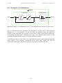
6.3.2 Principles of ΔΣ Modulation
System
Modulator
O
Demodulator
L
Q
Input
Output
integrator
quantizer
lowpass,
order > O
Fig 6.3.2: Principle of ΔΣ Modulation: An Oth order integrator and a quantizer within a loop
Fig. 6.3.2 illustrates the basic principle of ΔΣ modulation: A loop of an Oth order integrator
followed by a L - level quantizer. On the one hand, the quantizer makes the signal less
accurate, on the other hand, the accuracy is preserved as average of the faster clocked loop.
Consequently, demodulation is forming the average of the quantized data stream Q. This
averaging within baseband frequencies is performed by the lowpass.
As illustrated in Fig. 6.3.2 the "delta" (Δ) is the difference between input signal and quantized
output signal Q. The integrator, symbolized by the Greek letter "sigma" (Σ), sums all
deviations between input signal and Q while the loop seeks to minimize this sum.
- 34 -
M. Schubert
Getting Started with DE2 and DA2 Boards
Regensburg Univ. of Appl. Sciences
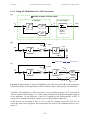
6.3.3 Using ΔΣ Modulation for D/A Conversion
(a)
Digital-to-Ananlog Converter (DAC)
Digital Modulator
Din
n
O
L
Demodulator
Q
integrator
L-level
DAC
quantizer
analog
lowpass,
order > O
(b)
8
fS2
Digital Modulator
(upsampling and digitalto-digital modulation within Altera FPGA)
Uout
UQ
lowpass
DQ
DAC2
(9 level)
fS1
Uout2
9 level
red
Uout2,C
R
C
white
=10fS2
Fig 6.3.3: (a) Using ΔΣ Modulation for D/A Conversion. (b) Realization in this lab.
Fig 6.3.3 illustrates the principle of using an ΔΣ modulator for D/A conversion. We have a
completely digital modulator with digital input Din and digital output DQ. The quantizer can
be realized by simply omitting some of the lower significant bits, in the extreme situation DQ
is one bit only. To compensate for the loss of lower significant bits we have an increased
clock output speed fS1 = K1·fS2. The DAC is required to translate the output signal from digital
to analog domain.
In this lab we have K1 = 10 (consequently fS1 = 10·fS2).
In this lab DAC2 of the DA2 board is fed with an 8-bit / 9-level thermometric code. Its
possible states are "00000000" , "00000001", "00000011", "00000111", "00001111",
"00011111", "00111111", "01111111", "11111111". The output levels are shown as red
curves in Figs. 6.2 and 6.4.
In this lab the Digital-to-digital (D/D) modulator has a 1st order integrator. Consequently, the
demodulator would require at least 2nd order lowpass to exploit possible signal-to-noise ratio
(SNR). Here we yielded optically acceptable results with a simulated 1st order RC lowpass,
shown as white curve in Fig. 6.2.
- 35 -
M. Schubert
Getting Started with DE2 and DA2 Boards
Regensburg Univ. of Appl. Sciences
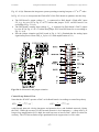
6.3.4 Using ΔΣ Modulation for A/D Conversion
(a)
Analog-to-Digital Converter (ADC)
Modulator
Uin
O
Demodulator
Q
L - level
ADC
n
Dout
digital
lowpass,
order > O
L - level
DAC
(b)
m
1st order
JP2
Uin
s1
E11
IN2
Uout
E9
OUT2 2nd
IN1
E3
E5
E10
E1
s2
OUT1
s3
Ufb,in
E6
E4
E2
DS2 board
(c)
JP2
Uin
s1
E11
IN2
OUT2 2nd
1st order
Uout
E9
E5
E10
IN1
DA2 board
E3
E1
s2
OUT1
Flash
ADC
Q
9 Level
s3
Ufb,in
DAC3
E6
E4
E2
Fig 6.3.4-1: (a) Principle of using ΔΣ Modulation for A/D Conversion. (b) Analog integrator
loop of DS2 board. (c) Incorporation of ADC and DAC makes analog loop to ΔΣ modulator.
To build a ΔΣ modulator for A/D conversion we use an analog integrator of Oth order and an
ADC as quantizer that translates Uout of the analog integrator to the quantized digital output Q
of the modulator. As the difference Δ has to be computed in the analog domain, a DAC is
required to re-translate the digital output Q to the analog feedback signal Ufb,in.
In this lab we use according to Figs. 6.3.4-1 (a) and (b) a jumper on pins E9, E10, E11 to
switch the order of the integrator and consequently the order of the modulator between O=1
and O=2.
- 36 -
M. Schubert
Getting Started with DE2 and DA2 Boards
Regensburg Univ. of Appl. Sciences
Fig. 6.3.4-1(b) illustrates the integrator system operating as analog lowpass of 1st or 2nd order.
In Fig. 6.3.4-1(c) we incorporate the Flash-ADC of the DA2 board as quantizer into the loop.
The DS2-board’s output voltage Uout is connected to DA2-baord’s Flash-ADC input
CP_in_p by wire W2 in Fig. 6.3.4-2. Confirm that jumper E1-E3 on DS2 board is set
according to Fig. 5.1.1(d).
The DS2-board’s analog input voltage Ufb,in is connected to DA2-baord’s DAC3 output
by wire W3 in Fig. 6.3.4-2. Confirm that jumper E2-E4 on DS2 board is set according to
Fig. 5.1.1(d).
Plot the jumper situation on DA2 board in Fig. 6.3.4-2. (Remind that the analog input
signal must proceed from TRS_in_Left to A33 with amplification of 10.)
Fig 6.3.4-2: Schematics and jumper situation
Control-Loop Point of View
Note that the ΔΣ ADC operates a DAC as feedback branch. According to control loop theory
STF
A
kA|
|
k 1 ,
1 kA
NTF
1
kA|
|
0
1 kA
with forward network A being integrator and quantizer here, and feedback network k being
the DAC. While the accuracy of the forward network is less important (→ cheap ADC!) as
long as loop amplification |kA| is high, the total loop acts as inverse DAC, which is critical for
accuracy. The NTF shows that average quantization noise suppression is of Oth order.
- 37 -
M. Schubert
Getting Started with DE2 and DA2 Boards
Regensburg Univ. of Appl. Sciences
6.4 Hardware Test Using Quartus II 8.1
Remove jumper A25-A27 so that there is only a jumper A35-A37 on the DE2 board while the
ΔΣ modulator on the DS2 board is connected by the respective jumpers. Start Quartus II 8.1
and use File → Open Project → to open project file
adac_StudentVersion/QuartusII81/tb_de2_adac/de2_adac.qpf
Alternatively you can double-click left on this file. Make sure that the DE2 board is ON, the
switch left to the 7-segment displays is set to RUN, the USB bus is connected to your computer
and the hardware driver of the Programmer is USB-Blaster.
Then select: Tool → Programmer → Add File... → de2_adac_demo.sof
Make sure that only flag Program/Configure is set and click Start. Now you should obtain
the results illustrated below.
Fig 6.4: Oscillogram: Uin (yellow) and Q=Ufb,in (green) of DS2 board, Uout1 (blue), Uout2 (red).
Feed a sinusoidal 1KHz signal with amplitude of 200mVpp to TRS_in_Left (pin A34) of
DA2 board and measure the 10 x amplified 2Vpp signal at pin A33. If necessary trim DA2board’s poti R1 such, that the wave is sinusoidal at pin A33. Then change the from a
sinusoidal to a rectangular signal to obtain the oscillogram shown above in Fig. 6.4.
The curves seen in the oscillogram in Fig. 6.4 are:
CH1: Top yellow smooth curve: Uin to DS2 board, measured at pin DA2_A33 = DS2_s1,
the rectangular curve got oscillations from DA2-board OpAmp OA4.
CH2: Top green 9-level curve = ΔΣ modulator’s output Q from flash-ADC, measured as
output of DAC3 (pin DA2_A25) = input Ufb,in of DS2 board.
- 38 -
M. Schubert
Getting Started with DE2 and DA2 Boards
Regensburg Univ. of Appl. Sciences
CH3: Blue: Output of R2R-DAC named DAC1 (pin DA2_A1), 256-level, being the
visualization of ΔΣ -ADC output DigSig. The time delay of 65 cycles of sampling clock
fS2 is due to the ΔΣ -demodulator (=lowpass).
CH4: Lower red 9-level curve: Output Uout2 of ΔΣ DAC named DAC2 (pin DA2_A17).
Input was the ADC’s output DigSig (blue). The time delay compared to CH3 is due to the
interpolation sinc4 filter.
Use of Switches sw(17 DOWNTO 0):
Switches sw(2:0) set the sampling frequency of the system according to
fs0=fs1=10fs2=10sw(2:0). A good setting is sw(2:0) = 1012 = 510. Then fS0=fS1=105Hz=
100KHz and fS2=10KHz allowing to display sound up to fS2/2 = 5KHz. Lower clock rates
are problematic because sound is limited to ½·fS2=500Hz; for higher sampling rates the
analog boards have problems to follow, because then fS0=fS1 ≥ 1MHz.
Switches sw(17:16) set the number of levels of the Flash-ADC according to
L = 2sw(17:16)+1. Consequently, sw(17:16)="11" → L=9, "10" → L=5, "01" → L=3,
"00" → L=2. While the Flash-ADC always delivers 9 levels, they are reduced by logic. In
Figs. 6.2 and 6.4 we have L=9 levels.
Switches sw(15:12) are meaningless here.
Questions:
Observe Fig. 6.4. Is the modulator again fast (green following yellow curve)? ...yes...
Observe Uout1 (DAC1out, blue). Ho swallowed the rectangular edges of Uin (yellow)?
..............................................................
Observe from Fig. 6.4 if the modulator is operated at 1st or 2nd order. To do so keep in mind,
that a 1st order modulator will never do jumps over 2 Δ’s with out significant changes jumps
on the input signal.
..............................................................
..............................................................
..............................................................
Students with the job of digital filter construction can now begin to fill the digital filters in
directory adac_StudentVersion/VHDL/architectures with logic until they obtain the
same results. More detailed information about the total system is given in [12].
- 39 -
M. Schubert
Getting Started with DE2 and DA2 Boards
Regensburg Univ. of Appl. Sciences
7 Conclusions
The reader learns how to start the Terasic / Altera DE2 board and to program its Altera
Cyclone II FPGA with VHDL using the Quartus II software. Some basic functions like
reading out switches and controlling LEDs are introduced before learning how to read from
and write to the board’s general-purpose input/output (GPIO) expansion headers.
The GPIO expansion headers are the used to connect the school’s DA2 daughter board and
control its circuit blocks, namely three DACs, a 9-level flash-ADC and an instrumentation
amplifier.
The DA2 daughter board connects the DS2 grandchild board containing the analog part of a
ΔΣ A/D Converter.
At the end all the components mentioned above are simulated using ModelSim and then
realized in hardware using Quartus II 8.1 software, the Terasic/Altera DE2 board and the selfmade daughter boards DA2 and DS2.
8 References
[1]
[2]
[3]
[4]
[5]
[6]
[7]
[8]
Available: http://www.terasic.com
Available: http://www.altera.com
Available: http://www.4shared-china.com/web/preview/pdf/WDmiLTCx, Sep. 2014
http://users.ece.gatech.edu/~hamblen/DE2/DE2_Schematic.pdf
Available at HSR: K:\SB\Hardware\Altera\DE2\DE2-CD\
Available: http://www.altera.com/literature
https://hps.hs-regensburg.de/~scm39115/homepage/education/courses/ada/ada.htm
https://hps.hs-regensburg.de/~scm39115/homepage/education/courses/sc/sc.htm,
User="student", Password="studaccept".
[9] HSR: k:\Sb\Software\Measurement&Test\TestToneGenerator (license for private use!)
[10] Timo Esser, Test Tone generator, available: http://kostenlose.rbytes.net/test-tone-generator_download/
[11] Available: https://hps.hs-regensburg.de/scm39115/homepage/education/courses/red/red.htm,
User="student", Password="studaccept".
[12] ADAC Project Reference Manual [11] → ADAC_Project_Reference_Manual.pdf.
- 40 -