1
B&K 4370 Accelerometer
and Charge Amplier Manual
L. Vicci
Microelectronic Systems Laboratory
Department of Computer Science
University of North Carolina at Chapel Hill
21Jan003
Summary
The Bruel&Kjr 4370 is a single axis piezoelectric accelerometer
sensitive along its Z axis down to nearly 10g], and conventionally useful over a range of 0.1Hz] up to about 1/3 of its mechanical resonance
frequency of 15{21kHz], depending on its mounted conguration. The
charge available on its output is proportional to acceleration sensed by
the device (including gravity). To be useful, this charge must be integrated by a charge amplier to provide a voltage proportional to acceleration. The overall low frequency performance depends on the limiting
noise oor and frequency response of the charge amplier
A charge amplier was designed specically for extending the useful
low end of the frequency range of the 4370 to 0.01Hz], and to provide
anti-alias ltering for adequately suppressing frequencies at the mechanical resonance of the accelerometer. This lter is a fth order Cauer
lter with zeros in the stop band to cancel the mechanical resonance.
It provides a at frequency response to its upper 3dB] cuto frequency
at 6.8kHz] and guarantees at least 20dB] anti-alias suppression of all
acceleration stimuli above 11kHz].
This report comprises a user manual for the accelerometer and
charge amplier kit, a theory of operation section, and an appendix
containing the design drawings. Casual users need not delve further
than the user manual, although the theory of operation provides more
detailed technical insights which will be useful to the more serious user.
The design drawings along with the theory of operation are intended
to be suciently detailed for anyone skilled in the art to adapt and
construct the charge amplier design for other accelerometers.
TR03-002
UNC Chapel Hill, Department of Computer Science
page 1
L. Vicci
B&K 4370 Accelerometer and Charge Amplier Manual
21Jan003
1 User Manual
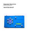
The accelerometer and charge amplier (Charge Amp) are provided as a complete
kit, and should always be kept together. The special coaxial cable provided to connect the
accelerometer to the charge amplier is a calibrated component with microdot connectors
which will not mate with any of the standard connector families. To encourage keeping
the kit together, a convenient carrying case is provided. A usage synopsis is posted on the
inside of the case.
Use of the kit is straightforward. All
that's necessary is to power the Charge Amp,
mount the accelerometer on the device under
test (DUT), connect them together and to
a data acquiring instrument such as a DAQ
card or oscilloscope, and set the gain and low
frequency cuto switches.
To power the Charge Amp, a 9-volt battery should be snapped into the front panel
receptacle. To prevent damage from battery
leakage, the Charge Amp should never
be stored with the 9-volt battery in- Figure 1: Kit consists of an accelerometer,
stalled. The external battery access feature a cable, a charge amplier (shown with batis intended to make it convenient to observe tery installed), and a carrying case.
this rule. Also please note the polarity of the
snap connectors and do not attempt to install the battery backwards.
The accelerometer should be mounted to the device under test (DUT) using either
a 10-32 fastener or double backed adhesive tape. Under no circumstances should
the fastener be forcibly threaded into the accelerometer. Slightly over two complete turns is the maximum thread depth in the 4370. The manufacturer's recommended
mounting techniques for threaded fasteners and alternatives are excerpted from B&K02]
and shown here as Figures 2a and 2b.
The charge amplier should be set for the desired gain and low frequency cuto. Be
aware that the lower frequency ranges may take a long time to settle: over a minute for
the 0.01Hz] range. Settling can be hastened somewhat by briey switching to a higher
frequency range and back, but it will still take some time. Even when completely settled,
there is a residual DC error voltage of a few millivolts. If very high accuracy is desired,
this should be measured and subtracted from subsequent data.
The output voltage range of the Charge Amp is nominally 2:5V]. Depending on
battery voltage, the output will clip at 2:9V] or less. If the Charge Amp is overloaded
to clipping, its DC oset will be upset and must be allowed to re-settle before meaningful
measurements can be made. The remedy for this is either to use a less sensitive gain range
so that overload does not occur, or to use a low cuto range that settles acceptably quickly
after an overload.
The noise oor of the Charge Amp is on the order of 100Vrms ] on all ranges. On
the most sensitive range, this corresponds to an acceleration noise oor of approximately
100g]. As of this writing, these measurements are very approximate, and need to be
TR03-002
UNC Chapel Hill, Department of Computer Science
page 2
L. Vicci
B&K 4370 Accelerometer and Charge Amplier Manual
21Jan003
Figure 2a: Mounting techniques excerpted from B&K02]
quantied more carefully if the kit is to be used at sensitivities where this is an issue.
The upper cuto frequency, or 3dB] rollo point of the Charge Amp's passband is
nominally 6.8kHz]. In the stopband, a special rejection band is provided to suppress the
resonance peak of the accelerometer over the range of 15{21kHz] in which it can occur.
This provides at least 20dB] anti-alias ltering for all mechanical excitation above 11kHz],
TR03-002
UNC Chapel Hill, Department of Computer Science
page 3
L. Vicci
B&K 4370 Accelerometer and Charge Amplier Manual
21Jan003
Figure 2b: Alternative techniques excerpted from B&K02]
irrespective of the accelerometer resonance. Refer to page 13 of the design drawings for
detailed response curves, as simulated by SPICE.
The output of the charge amplier will drive any single-ended instrument input
impedance of 50] through a conventional BNC cable. It should be relatively insensitive to ground loops between the accelerometer and the driven instrument. However care
should be taken to prevent the Charge Amp box from electrically contacting anything,
as ground loops between the accelerometer and the Charge Amp itself can cause noise
problems. The Charge Amp is furnished with rubber feet to help provide the necessary
electrical isolation.
TR03-002
UNC Chapel Hill, Department of Computer Science
page 4
L. Vicci
B&K 4370 Accelerometer and Charge Amplier Manual
21Jan003
2 Charge Amp Theory of Operation
The Charge Amp is logically composed of ve functional blocks and a power management block. Referring to Figure 3, these are the charge integrating preamplier preamp,
two stages of anti-alias lter cauer1 and cauer2, an integrating feedback circuit dcfb, an
output driver diout, and power management pwrgnd. Also shown is an electrical model
tdcr of the accelerometer in which the acceleration stimulus is represented by voltage Va.
R0m
out
R5
7
R4
6
R6n
R3
5
4
C2
R2m
3
U2a
R1m
2
in
Notes:
1. R6 and C0 are gang
switchable for three
gain ranges.
2. R1, R2, and R0 are
gang switchable for
four low cutoff points.
U1b
dcfb
0
R6
2
R1
qout
ain
0
-
C5
U1a
Cs
+
C0n
sum
in
Cp
U3b
Va
C1
-
C5
C3
1
-
R4
in
out
U4b
C1
3
preamp
R1
U4a
R2
in
1
R3
C4
4
R2
+
+
U3a
R3
C4
4
0
2
R4
in
out
C2
R6
tdcr
C3
1
-
out
U2b
out
R4
R2
+
com
2
C4
3
cauer1
cauer2
R1
R1
0
0
R3
diffout
0
Vp
0
TITLE
U5
U1
U2
U3
C0
B1
Vn
pwrgnd
U4
MSL
DRAWN BY
DATE
Leandra Vicci
30 Dec, 2002
B&K 4370 Charge amplifier
DESCRIPTION
Charge amplifier, 10[mHz] to 10[kHz]
with SPICE nodes and subckts shown
SIZE
A
DWG NO
SCALE
1: 1.5
REV
4.0
SHEET
1 OF 15
Figure 3: Charge Amp schematic showing SPICE subcircuits
2.1 pwrgnd
The Charge Amp uses a single 9-volt battery, and needs to have a local ground reference, preferably midway between the positive and negative power rails. This is generated
by U5, a TLE2426 Virtual Ground Generator. This local virtual ground is connected to
the instrument's case and through the connecting cable to the body of the 4370. It is
therefore important not to allow a ground loop to be established between the 4370 and the
Charge Amp. The Charge Amp has insulating rubber feet to isolate it from its supporting
surface.
TR03-002
UNC Chapel Hill, Department of Computer Science
page 5
L. Vicci
B&K 4370 Accelerometer and Charge Amplier Manual
21Jan003
2.2 diout
Ground loop noise between the Charge Amp and the instrument it drives is however
suppressed. U2b is embedded in a dierential amplier conguration which isolates the
local ground from the output common. This prevents a ground loop from occurring between
the Charge Amp and the driven instrument. The amount of ground noise suppression
depends on the CMRR of the dierential conguration of diout which should approach
40dB].
2.3 tdcr
The resonance of the 4370 is not explicitly modeled here, but the acceleration stimulus,
including gravity, is represented by Va. Changes in Va cause a charge transfer through the
transcapacitance element Cs. Parallel capacitance Cp comprises the parasitic capacitance
of the 4370 and its connecting cable. The transcapacitance gain was chosen to match the
manufacturer's sensitivity data so that Va = 1V] represents an acceleration of 1m/s2].
Note that this is strictly a simulation model.
2.4 preamp
This is the integrating amplier which transduces charge to voltage. The transelastance gain is the reciprocal of capacitance C0. The preamp also provides one real pole
to the fth-order anti-alias lter. The frequency of this pole is established by R1 and the
parallel combination of Cs and Cp. Gain ranges are implemented with switch selectable
capacitances of 1, 10, and 100nF] for C0. Operation at very low frequency requires an
amplier with a low noise oor as well as very low bias current. U1 is a TLC2202C dual
low-noise precision op amp
p implemented in TI's LinCMOS technology, with 1pA] typical
bias current and 30nV/ Hz] at 10Hz] (in the 1/f noise regime). TI97a]
2.5 cauer1 and cauer2
Each of these circuits provides two complex poles and two complex zeros to the antialias lter. These poles along with one real preamp pole implement a fth order low
pass Butterworth function. The four complex zeros provide the desired signal suppression
over the frequency range of 15.5kHz] through 21.4kHz] to cancel out the 4370 resonance.
Refer to pages 13{15 of the design drawings for a quantitative comparison. 15.5kHz] is
the resonance of the 4370 mounted on a very large DUT mass, while 21.4kHz] is the
resonance of the unmounted device. The circuits themselves are nullor realizations of
generalized impedance converter (GIC) derived biquadratic functions Chen95].
2.6 dcfb
This circuit sets the low frequency cuto of the Charge Amp. In combination with
the accelerometer transfer function and the preamp transelastance, it implements a critically damped second order high pass lter function (that is, second order Butterworth).
This function has two DC zeros and a pair of complex conjugate poles which set the cuto frequency.. This provides a 40dB/decade] rollo below the switch selectable cuto
frequencies of 10, 1, 0.1, and 0.01Hz] (see page 13 of the design drawings).
TR03-002
UNC Chapel Hill, Department of Computer Science
page 6
L. Vicci
B&K 4370 Accelerometer and Charge Amplier Manual
21Jan003
The dcfb circuit itself synthesizes the equivalent of a parallel RL circuit which is
connected across C0 in the preamp. Accounting for the combined DC gain A of the Cauer
lter sections we have,
0 R1 R3
R = RAR
R 2
4
1 R3 C2
L = R0 RAR
:
4
The equivalent feedback impedance of the preamp circuit is then,
Z0 = (1=Z 1+ sC ) = C1 s2 + s(! s=Q ) + !2 where
RL
0
0
0
s0 0
0 R1 R3 C 0
Q0 = p R = RAR
2 R C and
L=C0
2 4 2
r
AR4
1 =
!0 = pLC
R0R1R3C0C2 :
0
The lter poles come from the denominator of Z0 , with the cuto frequency determined
by !0 and the damping factor by Q0. These parameters are highly underconstrained in
that the number of determining component values (degrees of freedom) is large. Component values were chosen to implement the desired low cuto for the various ranges while
providing the desired Butterworth function for each range.
References
B&K02] \Product Data { Piezoelectric DeltaShear Accelerometers Uni-Gain, DeltaTron and Special Types," http://www.bksv.com/pdf/Bp0196.pdf,
Bruel&Kjr, October 24, 2002.
Chen95] Wai-Kan Chen, Ed., \The Circuits and Filters Handbook," CRC Press, 1995,
ISBN 0-8493-8341-2, pp 2392{2400.
TI97a] Texas Instruments Data Book, "Ampliers, Comparators, and Special Functions," Texas Instruments, 1997, SLYD011A, vol A, pp 3-767.
TI97b] Texas Instruments Data Book, "Ampliers, Comparators, and Special Functions," Texas Instruments, 1997, SLYD012A, vol B, pp 6-287 .
APPENDIX A { Design drawings
The following are the design drawings of the as-built Charge Amp.
TR03-002
UNC Chapel Hill, Department of Computer Science
page 7
B1
Va
ain
Cs
Cp
qout
tdcr
0
C0
0
in
U5
R1
0
U1a
C0n
R0m
0
U1
preamp
sum
out
Vn
Vp
in
R6n
out
7
R5
4
U2
+
3
1
2
U2a
R4
pwrgnd
U3b
C4
R4
C1
C5
R6
6
out
U4
C1
U4b
+
-
C4
3
1
-
+
2
U3
DATE
Leandra Vicci
30 Dec, 2002
DRAWN BY
A
SIZE
2
1
R3
diffout
C4
R4
U2b
com
out
B&K 4370 Charge amplifier
0
in
R2
C2
Notes:
1. R6 and C0 are gang
switchable for three
gain ranges.
2. R1, R2, and R0 are
gang switchable for
four low cutoff points.
R1
SCALE
DWG NO
1: 1.5
REV
4.0
SHEET
1 OF 15
Charge amplifier, 10[mHz] to 10[kHz]
with SPICE nodes and subckts shown
DESCRIPTION
TITLE
in
out
cauer2
R2
C3
R3
U4a
R1m
MSL
0
4
R4
2
R2m
U1b
3
R6
C5
C2
0
in
4
R1
cauer1
R2
C3
R3
U3a
dcfb
R3
R1
-
+
5
B1
D51
C50
Sw2c
U5
R1
R10a
R10b
R10c
R10d
R16a
R16b
U1a
U1
4
8
1
Sw2a
preamp
C51
3
2
C0a
C0b
C0c
7
1
R26
U2
C53
5
pwrgnd
4
8
C21
+
U3b
6
U2a
R14
C24
R24
C25
R15
C52
Sw2b
Sw1c
U3
4
8
1
dcfb
U4
4
8
7
C31
5
6
cauer2
C33
R33
U4a
Sw1a
R32
-
+
R31
DATE
Leandra Vicci
30 Dec, 2002
DRAWN BY
+
U4b
C34
2
3
5
6
Sw1b
MSL
U1b
R34
C35
R36
7
R12c
R12d
R12a
C12 R12b
C54
cauer1
C23
R23
U3a
R22
-
+
R21
2
3
3
2
R13
A
SIZE
7
diffout
C44
R44
U2b
R43
5
6
R42
C42
B&K 4370 Charge amplifier
R41
SCALE
DWG NO
1: 1.5
REV
4.0
SHEET
2 OF 15
Charge amplifier, 10[mHz] to 10[kHz]
Schematic Diagram
DESCRIPTION
TITLE
1
R11d
R11c
R11b
R11a
Resistors
R1 13.3K
R10a 1G
R10b 100M
R10c 10M
R10d 1M
R11a 6.2M
R11b 620K
R11c 62K
R11d 6.2K
R12a 6.2M
R12b 620K
R12c 62K
R12d 6.2K
R13 100K
R14 100K
R15 100K
R16a 1K
R16b 10K
R21 10K
R22 15K
R23 10K
R24 10K
R26 16.9K
R31 7.5K
R32 24.9K
R33 10K
R34 10K
R36 10K
R41 10.7K
R42 10K
R43 10.7K
R44 10K
DATE
Leandra Vicci
30 Dec, 2002
DRAWN BY
MSL
Capacitors
C0a 1.0nF
C0b 10nF
C0c 100nF
C12 5mF
C23 10pF
C24 10pF
C21 999.1pF
C25 987.4pF
C33 10pF
C34 10pF
C31 3.325nF
C35 330.3pF
C42 220pF
C44 220pF
C50 100uF
C51 0.1mF
C52 0.1mF
C53 0.1mF
C54 0.1mF
B&K 4370 Charge amplifier
A
SIZE
SCALE
DWG NO
1: 1.5
REV
4.0
SHEET
3 OF 15
Charge amplifier, 10[mHz] to 10[KHz]
Component list
DESCRIPTION
TITLE
ICs & Diodes
D51 1N4148
U1 TLC2202C
U2 TLE2142C
U3 TLE2142C
U4 TLE2142C
U5 TLE2426
11
R10a
16
15
10
20
-
U5
12
19
13
18
+
C50
R15
R16a
R16b
R10b
22
out
B+
C0a
D51
C0c
B-
R10c
14
C52
21
C0b
C42
R14
17
R10d
R13
1
U1
5
4
3
2
9
8
7
6
gnd
R1
R12a
R12b
R12c
R12d
R11a
R11b
R11c
R11d
R42
R41
R44
U2
C44
R43
C51
com
in
C12
C24
R21
R26
R23
U3
R24
R36
R33
U4
R31
DATE
Leandra Vicci
30 Dec, 2002
DRAWN BY
MSL
C23
C33
C34
R34
R32
R22
C35
C54
C25
C53
C31
A
SIZE
SCALE
DWG NO
1.8: 1
REV
4.0
SHEET
Charge amplifier, 10[mHz] to 10[kHz]
Board layout
4 OF 15
B&K 4370 Charge amplifier
DESCRIPTION
TITLE
C21
+
C12
C12
-
DATE
Leandra Vicci
30 Dec, 2002
DRAWN BY
MSL
B&K 4370 Charge amplifier
A
SIZE
SCALE
DWG NO
1: 1
REV
4.0
SHEET
5 OF 15
Charge amplifier, 10[mHz] to 10[kHz]
Mechanical relationships
DESCRIPTION
TITLE
C12
1.533
Note 2
4.233
0.358
1.000
1.108
Note 1
0.753
1.125
1.150
0.525
3.025
2.953
2.400
DATE
Leandra Vicci
30 Dec, 2002
DRAWN BY
MSL
B&K 4370 Charge amplifier
A
SIZE
SCALE
DWG NO
1: 1.2
REV
4.0
SHEET
6 OF 15
Charge amplifier, 10[mHz] to 10[kHz]
Box mechanicals
DESCRIPTION
TITLE
Notes:
1. Index from faces at the bottom of the box.
2. Index from face at the top of the box.
3. Box: Hammond Mfg. 1590CBK
2.715
2.980
4.375
0.567
1.067
1.202
1.368
1.415
1.103
2.868
3.202
2.603
2.290
#30 drill,
2 places
DATE
30 Dec, 2002
Leandra Vicci
MSL
DRAWN BY
1/8" drill,
2 places
3/8" drill,
2 places
cut with
3/16" end mill
B&K 4370 Charge amplifier
A
SIZE
SCALE
DWG NO
1: 1.2
REV
4.0
SHEET
7 OF 15
Charge amplifier, 10[mHz] to 10[kHz]
Box lid mechanicals
DESCRIPTION
TITLE
0.125
0.625
0.500
0.750
0.125
0.250
0.500
0.750
0.875
1.025
1.188
1.375
0.750
0.313
0.525
1.500
#36 drill
2.000
1.000
cut with
3/16" end mill
#36 drill, then tap
6-32 NC, 4 places
3/8 end mill,
2 places
#41 drill,
2 places
DATE
Leandra Vicci
30 Dec, 2002
DRAWN BY
MSL
B&K 4370 Charge amplifier
A
SIZE
SCALE
DWG NO
2: 1
REV
4.0
SHEET
8 OF 15
Charge amplifier, 10[mHz] to 10[kHz]
Battery holder mechanicals
DESCRIPTION
TITLE
Material: Rigid, non-brittle, machinable
insulator such as nylon or polypropylene.
1
OFF
1.0
10
LOW CUTOFF [Hz]
0.01
0.1
DATE
Leandra Vicci
30 Dec, 2002
DRAWN BY
MSL
CHARGE AMPLIFIER FOR B&K4370
RANGE [mV/m/s2]
100
10
B&K 4370 Charge amplifier
A
SIZE
SCALE
DWG NO
1: 1
REV
4.0
SHEET
9 OF 15
Charge amplifier, 10[mHz] to 10[kHz]
Front panel label
DESCRIPTION
TITLE
• Store with battery installed.
• Insert fastener more than 2
turns into accelerometer.
DO NOT
PLEASE DO
• Store all parts of kit together.
• Install 9-volt battery.
• Mount accelerometer and
connect to charge amplifier.
• Connect BNC connector to a
scope or other instrument.
• Upper cutoff frequency is
6.8[kHz].
INSTRUCTION SUMMARY
DATE
Leandra Vicci
30 Dec, 2002
DRAWN BY
MSL
B&K 4370 Charge amplifier
A
SIZE
SCALE
DWG NO
1: 1
REV
4.0
SHEET
10 OF 15
Charge amplifier, 10[mHz] to 10[kHz]
Carrying case and warning labels
DESCRIPTION
TITLE
Microelectronic Systems Laboratory, Department of Computer Science, UNCCH
B&K4370 ACCELEROMETER
AND CHARGE AMPLIFIER KIT
+
1.038 (1.025)
-
0.125
DATE
31 Dec, 2002
Leandra Vicci
MSL
DRAWN BY
Largest diagonal 1.175
Largest ht 0.668
largest wd 1.038
1.813 (1.70)
B&K 4370 Charge amplifier
A
SIZE
SCALE
DWG NO
2: 1
REV
4.0
SHEET
11 OF 15
Charge amplifier, 10[mHz] to 10[kHz]
9-volt battery
DESCRIPTION
TITLE
0.668 (0.65)
DATE
Leandra Vicci
16 Jan, 2003
DRAWN BY
MSL
B&K 4370 Charge amplifier
A
SIZE
SCALE
DWG NO
1: 1
REV
4.0
SHEET
12 OF 15
Charge amplifier, 10[mHz] to 10[kHz]
Circuit photos, top and bottom
DESCRIPTION
TITLE
Note: C42 and C44 were added
after these photos were taken.
Gain [db(V/m/s 2)]
1
[mHz]
-180
-160
-140
-120
-100
-80
-60
-40
-20
10
[mHz]
f
10
[m
Hz
]
lo
=
10
0
f
0
[m
Hz
]
lo
=
100
[mHz]
1
[H
f
=
lo
f
1
[Hz]
10
100
[Hz]
[Hz]
Frequency
DATE
Leandra Vicci
17 Jan, 2003
DRAWN BY
A
SIZE
100
[kHz]
1
[MHz]
B&K 4370 Charge amplifier
SCALE
DWG NO
1: 1
REV
4.0
SHEET
13 OF 15
Charge amplifier, 10[mHz] to 10[kHz]
SPICE simulations of as designed circuit
DESCRIPTION
TITLE
10
[kHz]
MSL
1
[kHz]
SPICE simulation of Charge Amplifier response curves for G 1k = 100 [mV/m/s 2]
z]
lo
=
10
[
H
z]
Gain [db(V/m/s 2)]
1
mHz
-140
-130
-120
-110
-100
-90
-80
-70
-60
-50
-40
-30
-20
-10
10
mHz
100
mHz
1
Hz
10
100
Hz
Hz
Frequency
G1k = 1 [mV/m/s^2]
G1k = 10 [mV/m/s^2]
G1k = 100 [mV/m/s^2]
DATE
A
SIZE
100
kHz
1
MHz
B&K 4370 Charge amplifier
SCALE
DWG NO
1: 1
REV
4.0
SHEET
14 OF 15
Charge amplifier, 10[mHz] to 10[kHz]
SPICE simulations of as designed circuit
DESCRIPTION
TITLE
10
kHz
Leandra Vicci
17 Jan, 2003
DRAWN BY
MSL
1
kHz
SPICE simulation of Charge Amplifier response curves for F lo = 10 [mHz]
Calibration Chart for
Accelerom..., Type 4370
--
j
Serial no .... BZ.l R.Q.Q....... .
A......_
Typical Temperatura Seneltivity Error
in dB rei. the Reference Values
Individual deviation max. ± 1 dB
'-ltMty at ......S.Q.... Hut ... .:1.~...... °C
Cllllle c.ecltance
~f
.....•....
..1./.0.......................
pF
c..... leneivitv••
......... }t,/Ua ....
pC/ms-2.or ...........<-t.l,k .... pC/g"
V. . . . leMitivity••
............~.2. ...
mV/ms-2,or .......... R.f,.fi..... mV/g
~...._(including cablel
.............
U.'-8. ....... pF
Maximum Tranaveraa Sanaitivity at 30Hz ... .'!I,D... %
Weltht ...............5.'-f,.O....... grams
Unc~Mnped natural frequency ........... 2.1, ........... kHz
For mountacl Reaonant Frequency and for Frequency
Reapoi'IH relative to Reference Sensitivity.... attachacl individual Frequency R81P0fl88 Curve
=center
an acceleration dir
into the body of the
of the c:qn_nector for
from lhe mounting surface
terom«er.
Realatence minimum
20000Mn~ room temperature.
Polerity is poeitive
Date
.2:-.J.a.~.-u ... Signa._.
::r;; ................ .
.........
• 1 g • 8,B07 ms-'-2
•• This calibration is traceable to the National Bureau
of Standards Washington D.C.
IIC 01!10
+ 40
-d•'o1----s~o--~1+oo~~150~---2oo~--~250~--~3oo~•c
-,
W
32
122
Phy8ical:
302
312
482
572°F
79o39l
!:~
Material: Stainless Steel
IIi'I
Mounting Thread: 10-32 UNF-2B
Electrical Connector: Coaxial
10-32 UNF-2A thread
Environmental:
Humidity: Seaied
Max. Temperature: 250"C or 4B2°F
Max. Continuous Sinuaoidal Ace. (peakl:
20000ms-2or 2000g
Max. Shock Acceleration: 50000 ms-2 or 5000 g
Typical Magnetic Sensitivity (50 Hzl: f.2 m$-2/T or
0,012 g/kgauss
Typical Temperature Transient Sensitivity:
(Low. Lim. Freq.: 3 Hzl O.OB ms-2;oc or O.OOB g/°C
Typical Baee Strain Sensitivity:
0.003 ms-2/pstrafn or 0,0003 g/pstrain
For further information see B & K "Piezoelectric Accelerometer and Preamplifier" Handbook.
Potentiometer:
pate:
212
D A 8
Zero Level:
C Lin.
{
dB
+ 30
·--
+ 20
+10
I
j
:
0
-10
\
)0
500
n. Fr~.: _ _ _ _ Hz
1 kHz
2
5
Writing. Speed: _ _ _ _ mm/~c.
10
20
50
100
'Paper Speed: _ _ _ _ mm/sec.
I
-