1
UM1714
User manual
Evaluation board for STM32 F0 series
with STM32F072VB MCU
Introduction
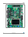
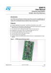
The STM32072B-EVAL evaluation board is designed as complete demonstration and
development platform for STMicroelectronics ARM cortex-M0 core-based STM32F072VBT6
microcontroller with two I2C, two SPI, four USART, one CAN, 12bit ADC, 12bit DAC, two GP
comparators, internal 16KB SRAM and 128KB Flash, USB FS, Touch sensing, CEC, SWD
debugging support.
The full range of hardware features on the board is designed for the evaluation of all the
peripherals (for example the motor control connector, USB full-speed, RS232, RS485,
Audio DAC, microphone ADC, Touch sensing buttons, TFT LCD, CAN, IrDA, IR LED, IR
receiver, LDR, MicroSD card, CEC on two HDMI connectors, Smart card slot, RF E2PROM
and the temperature sensor) and for the development of user-specific applications.
Extension headers are used to easily connect a daughter board or wrapping board for the
user-specific applications.
The ST-LINK/V2 is integrated on the board as embedded in-circuit debugger and
programmer for the STM32 MCU.
January 2014
DocID025744 Rev 1
1/63
www.st.com
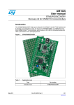
UM1714
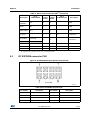
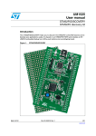
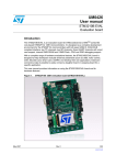
Figure 1. STM32072B-EVAL evaluation board picture (1)
1. Picture not contractual
2/63
DocID025744 Rev 1
UM1714
Contents
Contents
1
2
3
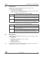
Overview . . . . . . . . . . . . . . . . . . . . . . . . . . . . . . . . . . . . . . . . . . . . . . . . . . 7
1.1
Features . . . . . . . . . . . . . . . . . . . . . . . . . . . . . . . . . . . . . . . . . . . . . . . . . . . 7
1.2
Demonstration software . . . . . . . . . . . . . . . . . . . . . . . . . . . . . . . . . . . . . . . 7
1.3
Order code . . . . . . . . . . . . . . . . . . . . . . . . . . . . . . . . . . . . . . . . . . . . . . . . . 7
1.4
Delivery recommendations . . . . . . . . . . . . . . . . . . . . . . . . . . . . . . . . . . . . . 8
Hardware layout and configuration . . . . . . . . . . . . . . . . . . . . . . . . . . . . . 9
2.1
Development and debug support . . . . . . . . . . . . . . . . . . . . . . . . . . . . . . . .11
2.2
Power supply . . . . . . . . . . . . . . . . . . . . . . . . . . . . . . . . . . . . . . . . . . . . . . 12
2.3
Clock source . . . . . . . . . . . . . . . . . . . . . . . . . . . . . . . . . . . . . . . . . . . . . . . 15
2.4
Reset source . . . . . . . . . . . . . . . . . . . . . . . . . . . . . . . . . . . . . . . . . . . . . . 15
2.5
Boot option . . . . . . . . . . . . . . . . . . . . . . . . . . . . . . . . . . . . . . . . . . . . . . . . 16
2.6
Audio . . . . . . . . . . . . . . . . . . . . . . . . . . . . . . . . . . . . . . . . . . . . . . . . . . . . 16
2.7
RS232, RS485 and IrDA . . . . . . . . . . . . . . . . . . . . . . . . . . . . . . . . . . . . . 17
2.8
Touch sensing buttons . . . . . . . . . . . . . . . . . . . . . . . . . . . . . . . . . . . . . . . 19
2.9
MicroSD card . . . . . . . . . . . . . . . . . . . . . . . . . . . . . . . . . . . . . . . . . . . . . . 20
2.10
Analog input . . . . . . . . . . . . . . . . . . . . . . . . . . . . . . . . . . . . . . . . . . . . . . . 20
2.11
LDR (Light Dependent Resistor) . . . . . . . . . . . . . . . . . . . . . . . . . . . . . . . 20
2.12
Temperature sensor . . . . . . . . . . . . . . . . . . . . . . . . . . . . . . . . . . . . . . . . . 21
2.13
USB . . . . . . . . . . . . . . . . . . . . . . . . . . . . . . . . . . . . . . . . . . . . . . . . . . . . . 21
2.14
Smart card . . . . . . . . . . . . . . . . . . . . . . . . . . . . . . . . . . . . . . . . . . . . . . . . 21
2.15
CAN . . . . . . . . . . . . . . . . . . . . . . . . . . . . . . . . . . . . . . . . . . . . . . . . . . . . . 22
2.16
RF E2PROM . . . . . . . . . . . . . . . . . . . . . . . . . . . . . . . . . . . . . . . . . . . . . . 23
2.17
HDMI CEC . . . . . . . . . . . . . . . . . . . . . . . . . . . . . . . . . . . . . . . . . . . . . . . . 23
2.18
IR LED and IR receiver . . . . . . . . . . . . . . . . . . . . . . . . . . . . . . . . . . . . . . 23
2.19
Motor control . . . . . . . . . . . . . . . . . . . . . . . . . . . . . . . . . . . . . . . . . . . . . . 23
2.20
Display and input devices . . . . . . . . . . . . . . . . . . . . . . . . . . . . . . . . . . . . . 24
Connectors . . . . . . . . . . . . . . . . . . . . . . . . . . . . . . . . . . . . . . . . . . . . . . . 26
3.1
Motor control connector CN1 . . . . . . . . . . . . . . . . . . . . . . . . . . . . . . . . . . 26
3.2
RF E2PROM connector CN2 . . . . . . . . . . . . . . . . . . . . . . . . . . . . . . . . . . 27
DocID025744 Rev 1
3/63
4
Contents
4
UM1714
3.3
HDMI sink connector CN3 . . . . . . . . . . . . . . . . . . . . . . . . . . . . . . . . . . . . 28
3.4
User USB type B connector CN4 . . . . . . . . . . . . . . . . . . . . . . . . . . . . . . . 29
3.5
HDMI source connector CN5 . . . . . . . . . . . . . . . . . . . . . . . . . . . . . . . . . . 29
0.1
CAN D-type and 9-pin male connector CN6 . . . . . . . . . . . . . . . . . . . . . . . 30
3.6
Daughter board extension connector CN7 and CN8 . . . . . . . . . . . . . . . . 30
3.7
MicroSD connector CN9 . . . . . . . . . . . . . . . . . . . . . . . . . . . . . . . . . . . . . . 34
3.8
RS232 and RS485 connector CN10 . . . . . . . . . . . . . . . . . . . . . . . . . . . . 35
3.9
High-density SWD connector CN11
3.10
Standard SWD connector CN12 . . . . . . . . . . . . . . . . . . . . . . . . . . . . . . . . 37
3.11
ST-LINK/V2 USB type B connector CN13 . . . . . . . . . . . . . . . . . . . . . . . . 38
3.12
Audio jack CN14 . . . . . . . . . . . . . . . . . . . . . . . . . . . . . . . . . . . . . . . . . . . . 38
3.13
TFT LCD connector CN15 . . . . . . . . . . . . . . . . . . . . . . . . . . . . . . . . . . . . 38
3.14
ST-LINK/V2 programming connector CN16 . . . . . . . . . . . . . . . . . . . . . . . 38
3.15
Power connector CN17 . . . . . . . . . . . . . . . . . . . . . . . . . . . . . . . . . . . . . . 39
3.16
Analog input connector CN18 . . . . . . . . . . . . . . . . . . . . . . . . . . . . . . . . . 39
3.17
Smart card connector CN19 . . . . . . . . . . . . . . . . . . . . . . . . . . . . . . . . . . 40
. . . . . . . . . . . . . . . . . . . . . . . . . . . . 36
Schematics . . . . . . . . . . . . . . . . . . . . . . . . . . . . . . . . . . . . . . . . . . . . . . . 41
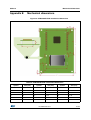
Appendix A STM32072B-EVAL IO assignment . . . . . . . . . . . . . . . . . . . . . . . . . . 57
Appendix B Mechanical dimensions. . . . . . . . . . . . . . . . . . . . . . . . . . . . . . . . . . . 61
Revision history . . . . . . . . . . . . . . . . . . . . . . . . . . . . . . . . . . . . . . . . . . . . . . . . . . . . 62
4/63
DocID025744 Rev 1
UM1714
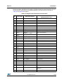
List of tables
List of tables
Table 1.
Table 2.
Table 3.
Table 4.
Table 5.
Table 6.
Table 7.
Table 8.
Table 9.
Table 10.
Table 11.
Table 12.
Table 13.
Table 14.
Table 15.
Table 16.
Table 17.
Table 18.
Table 19.
Table 20.
Table 21.
Table 22.
Table 23.
Table 24.
Table 25.
Table 26.
Table 27.
Table 28.
Table 29.
Table 30.
Table 31.
Table 32.
Table 33.
Table 34.
Table 35.
Table 36.
Third-party support of ST-LINK/V2 . . . . . . . . . . . . . . . . . . . . . . . . . . . . . . . . . . . . . . . . . . . 11
Power source related jumpers . . . . . . . . . . . . . . . . . . . . . . . . . . . . . . . . . . . . . . . . . . . . . . 12
Power-mode related Jumpers. . . . . . . . . . . . . . . . . . . . . . . . . . . . . . . . . . . . . . . . . . . . . . . 13
Low-voltage limitation . . . . . . . . . . . . . . . . . . . . . . . . . . . . . . . . . . . . . . . . . . . . . . . . . . . . . 14
32 kHz crystal X1 related solder bridges . . . . . . . . . . . . . . . . . . . . . . . . . . . . . . . . . . . . . . 15
8 MHz crystal X2 related solder bridges . . . . . . . . . . . . . . . . . . . . . . . . . . . . . . . . . . . . . . . 15
Boot-related switch . . . . . . . . . . . . . . . . . . . . . . . . . . . . . . . . . . . . . . . . . . . . . . . . . . . . . . . 16
Boot0-related jumpers . . . . . . . . . . . . . . . . . . . . . . . . . . . . . . . . . . . . . . . . . . . . . . . . . . . . 16
Audio-related jumpers. . . . . . . . . . . . . . . . . . . . . . . . . . . . . . . . . . . . . . . . . . . . . . . . . . . . . 16
RS232 and IrDA related jumpers . . . . . . . . . . . . . . . . . . . . . . . . . . . . . . . . . . . . . . . . . . . . 18
RS485 related solder bridges . . . . . . . . . . . . . . . . . . . . . . . . . . . . . . . . . . . . . . . . . . . . . . . 19
Touch sensing buttons related solder bridges . . . . . . . . . . . . . . . . . . . . . . . . . . . . . . . . . . 19
LDR related jumpers . . . . . . . . . . . . . . . . . . . . . . . . . . . . . . . . . . . . . . . . . . . . . . . . . . . . . . 21
Temperature sensor related solder bridge . . . . . . . . . . . . . . . . . . . . . . . . . . . . . . . . . . . . . 21
Connection between ST8024L and STM32F072VBT6. . . . . . . . . . . . . . . . . . . . . . . . . . . . 22
CAN related jumpers . . . . . . . . . . . . . . . . . . . . . . . . . . . . . . . . . . . . . . . . . . . . . . . . . . . . . 22
Motor control related jumpers . . . . . . . . . . . . . . . . . . . . . . . . . . . . . . . . . . . . . . . . . . . . . . . 24
LCD modules . . . . . . . . . . . . . . . . . . . . . . . . . . . . . . . . . . . . . . . . . . . . . . . . . . . . . . . . . . . 24
Motor control connector CN1 . . . . . . . . . . . . . . . . . . . . . . . . . . . . . . . . . . . . . . . . . . . . . . . 26
RF E2PROM connector CN2 . . . . . . . . . . . . . . . . . . . . . . . . . . . . . . . . . . . . . . . . . . . . . . . 27
HDMI Sink connectors CN3 . . . . . . . . . . . . . . . . . . . . . . . . . . . . . . . . . . . . . . . . . . . . . . . . 28
USB type B connector CN4 . . . . . . . . . . . . . . . . . . . . . . . . . . . . . . . . . . . . . . . . . . . . . . . . 29
HDMI Source connectors CN5 . . . . . . . . . . . . . . . . . . . . . . . . . . . . . . . . . . . . . . . . . . . . . . 30
CAN D-type and 9-pin male connector CN6 . . . . . . . . . . . . . . . . . . . . . . . . . . . . . . . . . . . . 30
Daughter board extension connector CN7 . . . . . . . . . . . . . . . . . . . . . . . . . . . . . . . . . . . . . 31
Daughter board extension connector CN8 . . . . . . . . . . . . . . . . . . . . . . . . . . . . . . . . . . . . . 32
MicroSD connector CN9 . . . . . . . . . . . . . . . . . . . . . . . . . . . . . . . . . . . . . . . . . . . . . . . . . . . 34
RS232 and RS485 connector CN10 . . . . . . . . . . . . . . . . . . . . . . . . . . . . . . . . . . . . . . . . . . 35
High-density SWD debugging connector CN11 . . . . . . . . . . . . . . . . . . . . . . . . . . . . . . . . . 36
Standard SWD debugging connector CN12 . . . . . . . . . . . . . . . . . . . . . . . . . . . . . . . . . . . . 37
USB type B connector CN13 . . . . . . . . . . . . . . . . . . . . . . . . . . . . . . . . . . . . . . . . . . . . . . . 38
Analog input-output connector CN18 . . . . . . . . . . . . . . . . . . . . . . . . . . . . . . . . . . . . . . . . . 39
Smart card connector CN19 . . . . . . . . . . . . . . . . . . . . . . . . . . . . . . . . . . . . . . . . . . . . . . . . 40
STM32072B-EVAL IO assignment . . . . . . . . . . . . . . . . . . . . . . . . . . . . . . . . . . . . . . . . . . . 57
STM32072B-EVAL mechanical dimensions . . . . . . . . . . . . . . . . . . . . . . . . . . . . . . . . . . . . 61
Document revision history . . . . . . . . . . . . . . . . . . . . . . . . . . . . . . . . . . . . . . . . . . . . . . . . . 62
DocID025744 Rev 1
5/63
5
List of figures
UM1714
List of figures
Figure 1.
Figure 2.
Figure 3.
Figure 4.
Figure 5.
Figure 6.
Figure 7.
Figure 8.
Figure 9.
Figure 10.
Figure 11.
Figure 12.
Figure 13.
Figure 14.
Figure 15.
Figure 16.
Figure 17.
Figure 18.
Figure 19.
Figure 20.
Figure 21.
Figure 22.
Figure 23.
Figure 24.
Figure 25.
Figure 26.
Figure 27.
Figure 28.
Figure 29.
Figure 30.
Figure 31.
Figure 32.
Figure 33.
Figure 34.
6/63
STM32072B-EVAL evaluation board picture (1) . . . . . . . . . . . . . . . . . . . . . . . . . . . . . . . . . . 2
Hardware block diagram . . . . . . . . . . . . . . . . . . . . . . . . . . . . . . . . . . . . . . . . . . . . . . . . . . . . 9
STM32072B-EVAL evaluation board layout . . . . . . . . . . . . . . . . . . . . . . . . . . . . . . . . . . . . 10
The LDR on STM32072B-EVAL . . . . . . . . . . . . . . . . . . . . . . . . . . . . . . . . . . . . . . . . . . . . 20
Motor control connector CN1 . . . . . . . . . . . . . . . . . . . . . . . . . . . . . . . . . . . . . . . . . . . . . . . 26
RF EEPROM daughter board connector CN2 . . . . . . . . . . . . . . . . . . . . . . . . . . . . . . . . . . 27
HDMI Sink connectors CN3 . . . . . . . . . . . . . . . . . . . . . . . . . . . . . . . . . . . . . . . . . . . . . . . . 28
USB type B connector CN4 . . . . . . . . . . . . . . . . . . . . . . . . . . . . . . . . . . . . . . . . . . . . . . . . 29
HDMI source connectors CN5 . . . . . . . . . . . . . . . . . . . . . . . . . . . . . . . . . . . . . . . . . . . . . . 29
CAN D-type and 9-pin male connector CN6 . . . . . . . . . . . . . . . . . . . . . . . . . . . . . . . . . . . 30
MicroSD connector CN9 . . . . . . . . . . . . . . . . . . . . . . . . . . . . . . . . . . . . . . . . . . . . . . . . . . . 34
RS232 and RS485 connector CN10 . . . . . . . . . . . . . . . . . . . . . . . . . . . . . . . . . . . . . . . . . . 35
High-density SWD debugging connector CN11 . . . . . . . . . . . . . . . . . . . . . . . . . . . . . . . . . 36
Standard SWD debugging connector CN12 . . . . . . . . . . . . . . . . . . . . . . . . . . . . . . . . . . . . 37
USB type B connector CN13 . . . . . . . . . . . . . . . . . . . . . . . . . . . . . . . . . . . . . . . . . . . . . . . 38
Power supply connector CN17 . . . . . . . . . . . . . . . . . . . . . . . . . . . . . . . . . . . . . . . . . . . . . 39
Analog input-output connector CN18 . . . . . . . . . . . . . . . . . . . . . . . . . . . . . . . . . . . . . . . . . 39
Smart card connector CN19 . . . . . . . . . . . . . . . . . . . . . . . . . . . . . . . . . . . . . . . . . . . . . . . . 40
STM32072B-EVAL schematic 1 . . . . . . . . . . . . . . . . . . . . . . . . . . . . . . . . . . . . . . . . . . . . . 42
STM32072B-EVAL MCU schematic 2 . . . . . . . . . . . . . . . . . . . . . . . . . . . . . . . . . . . . . . . . 43
STM32072B-EVAL schematic 3 . . . . . . . . . . . . . . . . . . . . . . . . . . . . . . . . . . . . . . . . . . . . . 44
STM32072B-EVAL schematic 4 . . . . . . . . . . . . . . . . . . . . . . . . . . . . . . . . . . . . . . . . . . . . . 45
STM32072B-EVAL schematic 5 . . . . . . . . . . . . . . . . . . . . . . . . . . . . . . . . . . . . . . . . . . . . . 46
STM32072B-EVAL schematic 6 . . . . . . . . . . . . . . . . . . . . . . . . . . . . . . . . . . . . . . . . . . . . . 47
STM32072B-EVAL schematic 7 . . . . . . . . . . . . . . . . . . . . . . . . . . . . . . . . . . . . . . . . . . . . . 48
STM32072B-EVAL schematic 8 . . . . . . . . . . . . . . . . . . . . . . . . . . . . . . . . . . . . . . . . . . . . . 49
STM32072B-EVAL schematic 9 . . . . . . . . . . . . . . . . . . . . . . . . . . . . . . . . . . . . . . . . . . . . . 50
STM32072B-EVAL schematic 10 . . . . . . . . . . . . . . . . . . . . . . . . . . . . . . . . . . . . . . . . . . . . 51
STM32072B-EVAL schematic 11 . . . . . . . . . . . . . . . . . . . . . . . . . . . . . . . . . . . . . . . . . . . . 52
STM32072B-EVAL schematic 12 . . . . . . . . . . . . . . . . . . . . . . . . . . . . . . . . . . . . . . . . . . . . 53
STM32072B-EVAL schematic 13 . . . . . . . . . . . . . . . . . . . . . . . . . . . . . . . . . . . . . . . . . . . . 54
STM32072B-EVAL schematic 14 . . . . . . . . . . . . . . . . . . . . . . . . . . . . . . . . . . . . . . . . . . . . 55
TFT LCD daughter board MB895 . . . . . . . . . . . . . . . . . . . . . . . . . . . . . . . . . . . . . . . . . . . . 56
STM32072B-EVAL mechanical dimensions . . . . . . . . . . . . . . . . . . . . . . . . . . . . . . . . . . . . 61
DocID025744 Rev 1
UM1714
Overview
1
Overview
1.1
Features
1.2
•
Four 5 V power supply options: power jack, ST-LINK/V2 USB connector, user USB
connector or daughter board
•
Stereo audio jack which supports a headset with microphone connected to DAC and
ADC of STM32F072VBT6.
•
2 G Byte (or more) SPI interface MicroSD card
•
I2C compatible serial interface temperature sensor
•
RF E2PROM
•
RS232 and RS485 communication
•
IrDA transceiver
•
IR LED and IR receiver
•
SWD debug support, ST-LINK/V2 embedded
•
240x320 TFT color LCD connected to SPI interface of STM32F072VBT6
•
Joystick with 4-direction control and selector
•
Reset and tamper buttons
•
Four color user LEDs and two LEDs as MCU low power alarm
•
Extension connector for daughter board or wrapping board
•
MCU voltage choice fixed 3.3 V or adjustable from 1.65 V to 3.6 V
•
USB full-speed connector
•
Touch sensing buttons
•
RTC with backup battery
•
CAN2.0A/B compliant connector
•
Light Dependent Resistor (LDR)
•
Potentiometer
•
Two HDMI connectors with DDC and CEC
•
Smart Card slot
•
Motor control connector
Demonstration software
The demonstration software is preloaded in the board Flash memory for easy demonstration
of the device peripherals in stand-alone mode. For more information and to download the
latest version available, please refer to the STM32072B-EVAL demonstration software
available on www.st.com.
1.3
Order code
To order the STM32F072VBT6 evaluation board, use the order code STM32072B-EVAL.
DocID025744 Rev 1
7/63
62
Overview
1.4
UM1714
Delivery recommendations
Before using the board for the first time, please verify that nothing was damaged during
shipment and that no components are unplugged or lost.
When extracting the board from its plastic container, please check that no component
remains in the bag.
The main components to verify are the following:
1.
The 8 MHz crystal (X2) which may have been removed from its socket by a shock.
2.
The MicroSD card which may have been ejected from the CN9 connector (right side of
the board).
3.
The dual-interface EEPROM board (ANT7-M24LR-A) which may have been unplugged
from the CN2 connector (top left corner of the board).
For all information concerning the version of the MCU used on the board, its specification
and possible related limitations, please visit the company web site to download the relevant
data sheet and errata sheet.
8/63
DocID025744 Rev 1
UM1714
Hardware layout and configuration
2
Hardware layout and configuration
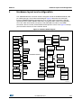
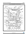
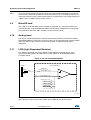
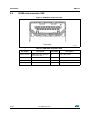
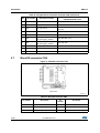
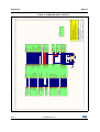
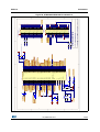
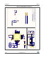
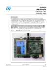
The STM32072B-EVAL evaluation board is designed around the STM32F072VBT6 (100pin LQFP package). The hardware block diagram Figure 2 illustrates the connection
between STM32F072VBT6 and peripherals such as motor control connector, USB fullspeed connector, RS232, RS485, Audio DAC, microphone ADC, Touch sensing buttons,
TFT LCD, CAN, IrDA, IR LED, IR receiver, LDR, MicroSD card, CEC on two HDMI
connectors, Smart card slot, RF E2PROM and Temperature sensor. The Figure 3 will help
you locate these features on the evaluation board.
Figure 2. Hardware block diagram
0RWRUFRQWURO
FRQQHFWRU
56
WUDQVFHLYHU
86$57
-R\VWLFN
9ROWDJH
WUDQVODWRU
*3,2
/('V
,U'$ WUDQVFHLYHU
7DPSHU
NH\EXWWRQ
3KRWR5
&RPSDUDWRU
86%
FRQQHFWRU
86%)6
&$1GULYHU
FRQQHFWRU
&$1
,5/('
,5UHFHLYHU
,57,0
3:0
3RWHQWLRPHWHU
(PEHGGHG
67/,1.9
6:'
FRQQHFWRU
670)9%7
63,
7HPSHUDWXUH
VHQVRU
,&
0LFUR6'
FDUG
$XGLR
DPSOLILHU ,&
+'0,
6RXUFH
5)((3520
FRQQHFWRU
9ROWDJH
WUDQVODWRU
'RW0DWUL[
/&'
&RPSDUDWRU
&(&
86%7\SH%
FRQQHFWRU
6:'
'$&
+'0,
VLQN
56
WUDQVFHLYHU
5656
&RQQHFWRU
+HDGVHW-DFN
$'&
76
FRQWUROOHU
86$57
0LFURSKRQH
DPSOLILHU
7RXFKVHQVLQJ
EXWWRQV
6PDUWFDUG
9WR9
DGMXVWDEOH
UHJXODWRU
7ZR9
UHJXODWRUV
([WHQVLRQ
FRQQHFWRUIRU
*3,2V
.47
DocID025744 Rev 1
9/63
62
Hardware layout and configuration
UM1714
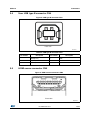
Figure 3. STM32072B-EVAL evaluation board layout
&1
5)((3520
GDXJKWHUERDUG
FRQQH
FWRU
7676
7RXFK%XWWRQV
&1
0RWRUFRQWURO
FRQQHFWRU
5
/'5
&1&1
([WHQVLRQ
KHDGHU
&1
+'0,
6LQN
&1
86%)6
&1
+'0,
6RXUFH
8
670)9%7
&1
&$1
&1
0LFUR6'FDUG
&1
86$57
56
56
&1
6:'FRQQHFWRU
&1
6:'FRQQHFWRU
8
,U'$
/'
,5/('
&1
67/,1.9
86%
&1
$XGLRMDFN
/'
67/,1.9
&20/('
'
,5UHFHLYHU
&1
3RZHU-DFN
FRORUV
/('V /RZYROWDJH
DODUP/('V
59 % 9''DGMXVWPHQW 5HVHWEXWWRQ
10/63
DocID025744 Rev 1
% WDPSHU
EXWWRQ
%
MR\VWLFN
59 SRWHQWLRPHWHU
.47
UM1714
2.1
Hardware layout and configuration
Development and debug support
The version 2 of the ST-LINK called ST-LINK/V2 is embedded on the board. This tool is
used for program loading and debugging of the STM32F072VBT6 on board using the SWD
interface. The third-party debug tools are also supported by SWD with connectors CN11 and
CN12.
A specific driver needs to be installed on your PC for the communication with the embedded
ST-LINK/V2.The install shield called ST-LINK_V2_USBdriver.exe is available on the
company website. To download and install this driver, please refer to the software and
development tools page for STM32F0 family available on www.st.com.
The third-party tool chains, Atollic TrueSTUDIO, KEIL ARM-MDK, IAR EWARM and the
Tasking VX-Toolset support ST-LINK/V2 according to Table 1.
Table 1. Third-party support of ST-LINK/V2
Third party
Toolchain
Version
Atollic
TrueSTUDIO
2.1
IAR
EWARM
6.20
Keil
MDK-ARM
4.20
TaskingVX-Toolset
ARM Cortex-M
4.0.1
The embedded ST-LINK/V2 is connected to the PC via a standard USB cable connected to
connector CN13.The bicolor LED LD9 (COM) indicates the status of the communication as
follows:
Note:
•
Slow blinking Red/Off: at power on before USB init
•
Fast blinking Red/Off: after the first correct communication between the PC and STLINK/V2 (enumeration)
•
Red Led On: when initialization between PC and ST-LINK/V2 is successfully complete
•
Green Led On: after successful target communication initialization
•
Blinking Red/Green: during communication with target
•
Red On: communication finished and OK
•
Orange On: communication failure
It is possible to power the board via CN13 (embedded ST/LINK/V2 USB connector) even if
an external tool is connected to CN11 (high-density SWD connector) or CN12 (SWD
connector).
DocID025744 Rev 1
11/63
62
Hardware layout and configuration
2.2
UM1714
Power supply
The STM32072B-EVAL evaluation board is power supplied by 5V DC supply and protected
by PolyZen in case of wrong power plug-in event. It is possible to configure the evaluation
board to use any of the four following sources for the power supply:
•
5V DC power adapter connected to CN17, the Power Jack on the board (Power Supply
Unit (PSU) on silk screen of JP19). The external power supply is not provided with the
board.
•
5V DC power with 500 mA limitation from CN13, the USB type B connector of STLINK/V2 (USB 5 V power source (STlk) on silk screen of JP19).
•
5V DC power with 500 mA limitation from CN4, the USB type B connector (USB 5 V
power source (U5V) on silk screen of JP19).
•
5V DC power from CN8, the extension connector for daughter board (daughter board
power source (D5V) on silk screen of JP19).
The power source is selected by setting the related jumpers JP19, JP11 and JP14 as
described in Table 2.
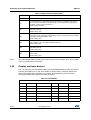
Table 2. Power source related jumpers
Jumper
Description
JP19 is used to select one of the four possible power supply resources.
For power supply jack(CN17) to the STM32072B-EVAL only, JP19 is set as shown
below
8967ON'9368
For power supply from the daughter board connectors(CN8) to STM32072BEVAL only, JP19 is set as shown below:
8967ON'9368
For power supply from USB (CN13) of ST-LINK/V2 to STM32072B-EVAL only, JP19
is set as shown below (default setting):
JP19
8967ON'9368
For power supply from USB (CN4) to STM32072B-EVAL only, JP19 is set as shown
below:
8967ON'9368
For power supply from power supply jack(CN17) to both STM32072B-EVAL and
daughter board connected on CN7 and CN8, JP19 is set as shown below (the
daughter board must not have its own power supply connected)
8967ON'9368
12/63
DocID025744 Rev 1
UM1714
Hardware layout and configuration
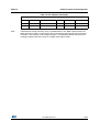
Table 2. Power source related jumpers (continued)
Jumper
Description
The Vbat pin of STM32F072VBT6 is connected to VDD when JP11 is set as shown
below (default setting):
JP11
ϭϮϯ
The Vbat pin of STM32F072VBT6 is connected to 3V battery when JP11 is set as
shown below:
ϭϮϯ
The VDDIO2 pin of STM32F072VBT6 is connected to 3.3V when JP14 is set as
shown below (default setting):
ϭϮϯ
JP14
The VDDIO2 pin of STM32F072VBT6 is connected to VDD_ADJ when JP14 is set
as shown below:
ϭϮϯ
Three power modes in total are supported on the board, and can be configured by setting
the related jumpers JP8, JP9, JP12, JP13 and JP16 as described in Table 3 and the
following notes.
•
Mode1: The VDD and VDDA was connected together & powered by fixed 3.3V.
•
Mode2: The VDD and VDDA was connected together & powered by adjustable voltage
from 1.65V to 3.6V.
•
Mode3: The VDD is powered by adjustable voltage from 1.65V to 3.6V while VDDA is
powered by fixed 3.3V.
Table 3. Power-mode related Jumpers
Power mode configuration
Power mode
JP13
JP8
VDD_MCU Idd measurement
(on JP12)
ϭϮϯ
ϭϮϯ
OK
ϭϮϯ
ϭϮϯ
NOT allowed
Mode1
DocID025744 Rev 1
13/63
62
Hardware layout and configuration
UM1714
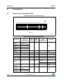
Table 3. Power-mode related Jumpers
Power mode configuration
Power mode
JP13
Note:
JP8
VDD_MCU Idd measurement
(on JP12)
Mode2
ϭϮϯ
ϭϮϯ
OK
Mode3
ϭϮϯ
ϭϮϯ
NOT allowed
VDD_MCU Idd measurement can be done by the current Ammeter which is mounted on
JP12 when it is open. VDDIO2 Idd measurement can be done by the current Ammeter
which is mounted on JP16 when it is open.
JP9 must be open (to disconnect VDDA from all analog power VDD_ANA which is
connected to analog circuits on the board) for MCU Idd measurement.
LD5 is lit when VDD<2V and in this case MCU is not functional. LD6 is lit when VDDA<2.4V
and in this case analogue parts in STM32F072VBT6 are not functional.
The LED LD7 is lit when the STM32072B-EVAL evaluation board is powered by the 5V.
Table 4 shows the low-voltage limitations that might apply depending on the characteristics
of some peripheral components. The components may work incorrectly when the power
level is lower than the limitation.
Table 4. Low-voltage limitation
Peripheral
Component
IO name
Low-voltage
limitation
Audio amplifier
U17
Audio input
2.2V(VDDA)
Microphone amplifier
U15
Audio output
2.7V(VDDA)
USB
CN4
USB
3V(VDDIO2)
CAN
CN6
CAN
3V(VDDIO2)
Smart Card
CN19
USART1
2.7V(VDDIO2)
Caution:
JP12 and JP16 must not be opened; otherwise STM32F072VBT6 will be damaged due to
the lack of power supply on its power pins.
Caution:
There is a risk of explosion if the battery is replaced with the wrong type of battery. Dispose
of used batteries according to the instructions.
14/63
DocID025744 Rev 1
UM1714
2.3
Hardware layout and configuration
Clock source
Two clock sources are available on STM32072B-EVAL evaluation board for
STM32F072VBT6 and RTC embedded.
•
X1, 32 kHz crystal for embedded RTC
•
X2, 8 MHz crystal with socket for STM32F072VBT6 microcontroller, it can be removed
from the socket when an internal RC clock is used.
Table 5. 32 kHz crystal X1 related solder bridges
Jumper
Description
PC14 is connected to 32 kHz crystal when SB14 is open. (Default setting)
SB14
PC14 is connected to the extension connector CN7 when SB14 is closed. In this
case R71 must be removed to avoid any disturbance due to the 32 kHz quartz.
PC15 is connected to the 32 kHz crystal when SB15 is open. (Default setting)
SB15
PC15 is connected to the extension connector CN7 when SB15 is closed. In this
case R72 must be removed to avoid any disturbance due to the 32 kHz quartz
Table 6. 8 MHz crystal X2 related solder bridges
Jumper
Description
PF0 is connected to the 8 MHz crystal when SB16 is open. (Default setting)
SB16
PF0 is connected to the extension connector CN8 when SB16 is closed. In this case
C31 and X2 must be removed.
PF1 is connected to the 8 MHz crystal when SB17 is open. (Default setting)
SB17
2.4
PF1 is connected to the extension connector CN8 when SB17 is closed. In such
case R73 must be removed to avoid any disturbance due to the 8 MHz quartz.
Reset source
The reset signal of STM32072B-EVAL evaluation board is low active and the reset sources
include the following:
Note:
•
Reset button B1
•
Debugging tools from SWD connector CN11 and CN12
•
Daughter board from CN8
•
Embedded ST-LINK/V2
•
RS232 connector CN10 for ISP.
The jumper JP15 is to be closed for RESET handled by pin8 of RS232 connector CN10
(CTS signal), please look in Section 2.7 for details.
DocID025744 Rev 1
15/63
62
Hardware layout and configuration
2.5
UM1714
Boot option
The STM32072B-EVAL evaluation board is able to boot from the following:
•
Embedded user Flash
•
System memory with boot loader for ISP
•
Embedded SRAM for debugging
The boot option is configured by setting the switch SW1 (BOOT0) and one option bit in
Small Information block (SIF). The BOOT0 can be configured also via RS232 connector
CN10.
Table 7. Boot-related switch
Switch
configuration
Bit12 in user
option bytes
0 <-> 1
X
STM32072B-EVAL boot from User Flash when SW1 and
bit12 in user option bytes set as shown on the left. (Default
setting)
0
STM32072B-EVAL boot from Embedded SRAM when SW1
and bit12 in user option bytes set as shown on the left.
1
STM32072B-EVAL boot from System Memory when SW1
and bit12 in user option bytes set as shown on the left.
SW1
0 <-> 1
SW1
0 <-> 1
SW1
Boot from
Table 8. Boot0-related jumpers
Jumper
JP5
2.6
Description
The Bootloader_BOOT0 is managed by pin 6 of connector CN10 (RS232 DSR
signal) when JP5 is closed. This configuration is used for boot loader application
only.
Default Setting: Not fitted
Audio
The STM32072B-EVAL evaluation board supports stereo audio playback and microphone
recording by an external headset connected on the audio jack CN14. Audio play is
connected to DAC output of STM32F072VBT6 through an audio amplifier and the
microphone on headset is connected to ADC input of STM32F072VBT6 through a
microphone amplifier. The audio amplifier can be enabled or disabled by setting JP20.
Mono/stereo playback is selected by setting JP18. Refer to Table 9 for detail.
Table 9. Audio-related jumpers
Jumper
Description
Speaker amplifier U17 is enabled when JP20 is closed (Default setting)
JP20
Speaker amplifier U17 is disabled when JP20 is open
16/63
DocID025744 Rev 1
UM1714
Hardware layout and configuration
Table 9. Audio-related jumpers (continued)
Jumper
Description
Mono playback is enabled when JP18 is set as shown below (default setting):
ϭϮϯ
.47
JP18
Stereo playback is enabled when JP18 is set as shown below:
ϭϮϯ
.47
The audio amplifier operates correctly when VDDA>2.2V and the microphone amplifier
operates correctly when VDDA>2.7V.
2.7
RS232, RS485 and IrDA
The communication of RS232 (with hardware flow control CTS and RTS) and RS485 is
supported on D-type 9-pin connector CN10. An IrDA transceiver (U14) is connected to
USART2 of the STM32F072VBT6. The signals Bootloader_RESET (shared with CTS
signal) and Bootloader_BOOT0 (shared with DSR signal) are added on RS232 connector
CN10 for ISP support.
The RS232 connector CN10 may be connected to either IOs of PD5 (USART2_TX) and
PD6 (USART2_RX) or IOs of PA14 (TX) and PA15 (RX) on STM32F072VBT6 MCU thanks
to the configuration jumpers JP7 and JP10. The bootloader is available only when RS232
connector is connected to PA14 and PA15. Please refer to Table 10 for details.
DocID025744 Rev 1
17/63
62
Hardware layout and configuration
UM1714
Table 10. RS232 and IrDA related jumpers
Jumper
Description
RS232_RX is connected to RS232 transceiver and RS232 communication is
enabled when JP17 is set as shown below (default setting):
56
56
,U'$ RS485_RX is connected to RS485 transceiver and RS485 communication is
enabled when JP17 is set as shown below:
56
56
,U'$ JP17
IrDA_RX is connected to IrDA transceiver and IrDA communication is enabled when
JP17 is set as shown below:
56
56
,U'$ PD5 is connected as TX signal when JP10 is set as shown to below (default setting):
ϭϮϯ
Note: bootloader is not supported with such configuration
JP10
PA14 is connected as TX signal when JP10 is set as shown below (JP2 must be
open in this case):
ϭϮϯ
Note: bootloader is supported with such configuration
PD6 is connected as RX signal when JP7 is set as shown below (default setting):
ϭϮϯ
Note: bootloader is not supported with such configuration
JP7
PA15 is connected as RX signal with bootloader being supported when JP7 is set
as shown below:
ϭϮϯ
Note: bootloader is supported with such configuration
JP2
18/63
SWCLK is connected to PA14 when JP2 is fitted.
Default setting: Fitted
DocID025744 Rev 1
UM1714
Hardware layout and configuration
The RS485 communication is supported by RS485 transceiver ST3485EBDR which is
connected to pin4 and pin9 of D-type 9-pins connectors CN10 (shared with USART2).
Table 11. RS485 related solder bridges
Jumper
2.8
Description
SB20,SB22
The external fail safe biasing are enabled when solder bridges SB20 and SB22 was
closed
Default setting: Not fitted
SB23
The bus termination is enabled when solder bridge SB23 is closed.
Default setting: Not fitted
SB21
The AC termination is disabled when solder bridge SB21 is closed for high baud rate
communication.
Default setting: Not fitted
Touch sensing buttons
Two touch sensing buttons are supported on STM32072B-EVAL evaluation board. These
are connected to three capacitive sensing channels (PD[12:14]) in group 8 with active shield
being connected to two capacitive sensing channels (PE4 and PE5) in group 7.
Table 12. Touch sensing buttons related solder bridges
Solder Bridge
Description
PD13 is used as Touch sensing button TS2 when SB12 is open. (Default setting)
SB12
PD13 is connected to the extension connector CN8 when SB12 is closed so touch
sensing button TS2 is not usable. If necessary R39 can be removed to avoid any
noise.
PD12 is used as Touch sensing button TS1 when SB13 is open (Default setting)
SB13
SB11
PD12 is connected to the extension connector CN8 when SB12 is closed so touch
sensing button TS1 is not usable. If necessary R40 can be removed to avoid any
noise.
PD14 is disconnect from the extension connector CN8 when SB11 is open (default
setting). In such case this IO is used as charge transfer pin connected to C17 for the
touch sensing application. (Default setting)
PD14 is connected to extension connector CN8 when SB11 is closed. In such case
C17 must be removed to avoid disturbance due to the capacitor
SB19
PE4 is disconnect from extension connector CN7 when SB19 is open (default
setting). In such case this IO is used as active shield for Touch sensing buttons TS1
& ST2.
PE4 is connected to the extension connector CN7 when SB19 is closed. In such
case R66 must be removed to avoid disturbance due to the shield
SB18
PE5 is disconnect from the extension connector CN7 when SB18 is open (default
setting). In such case this IO is used to manage the Shield capacitor C28 for the
touch sensing application.
PE5 is connected to the extension connector CN7 when SB19 is closed. In this case
R67 must be removed to avoid any disturbance due to the capacitor
DocID025744 Rev 1
19/63
62
Hardware layout and configuration
UM1714
Note:
the touch sensing buttons are fully functional only when STM32072B-EVAL is powered in
power mode 1 (both VDD & VDDA is connected to fixed 3.3 V). It is potentially necessary to
adjust the capacitor value of C28 and the firmware to adapt them to the voltage range from
1.65 V to 3.6 V of VDD in power modes 2 and 3.
2.9
MicroSD card
The 2 GB (or more) MicroSD card is available on the board. It is connected to SPI1 port
(shared with color LCD) of STM32F072VBT6. The MicroSD card detection is managed by
the standard IO port PB15 and it should be set with internal pull-up.
2.10
Analog input
The two-pin header CN18 and the 10K ohm potentiometer RV3 are connected to PC0 of
STM32F072VBT6 as analog input. A low pass filter can be implemented by replacing R206
and C113 with the right values of resistor and capacitor as requested by end user
application.
2.11
LDR (Light Dependent Resistor)
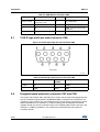
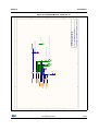
The VDDA is divided by the resistor bridge of LDR VT9ON1 and 8.2K resistor, and
connected to PA1 (COM1_IN+/ADC IN1) as shown below on the STM32072B-EVAL
evaluation board.
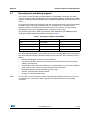
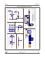
Figure 4. The LDR on STM32072B-EVAL
*3FRPSDUDWRU
9''$
.
$'&,1
* 3&2 03B ,1
3$ /'5
1&
* 3&2 03B ,1
* 1'
%DQG JDS 9
ó%DQG JD S
ò%DQG JD S
ô%DQG JD S
'$&2 87
.47
It is possible to compare LDR output with 1/4 band gap, 1/2 band gap, 3/4 band gap, band
gap and DAC1 OUT, and to connect LDR output to ADC IN1 for AD conversion.
20/63
DocID025744 Rev 1
UM1714
Hardware layout and configuration
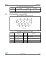
PA1 is also shared with the motor control bus voltage signal and its input source can be
selected by setting JP6 in Table 13.
Table 13. LDR related jumpers
Jumper
Description
PA1 is used as LDR input when JP6 is set as shown below (default setting):
ϭϮϯ
JP6
PA1 is used as motor control Bus Voltage signal when JP6 is set as shown below:
2.12
ϭϮϯ
Temperature sensor
A temperature sensor STLM75M2F is connected to I2C1 bus of STM32F072VBT6, and
shares the same I2C1 bus with RF E2PROM and DDC on HDMI_Source connector CN5.
The I2C address of the temperature sensor is 0b100100x, where x can be 0 or 1 depending
on the setting of SB6.
Table 14. Temperature sensor related solder bridge
Solder Bridge
Description
I2C address A0 is 0 when SB6 is open. (Default setting)
SB6
I2C address A0 is 1 when SB6 is closed.
Note:
the temperature result measured from STLM75M2F can be a little higher than the ambient
temperature due to the power dissipation of the components on the board.
2.13
USB
STM32072B-EVAL evaluation board supports USB2.0 compliant full speed communication
via a USB type B connector (CN4). The evaluation board can be powered by this USB
connection at 5 V DC with 500 mA current limitation.
USB operates correctly when VDDIO2>3V.
2.14
Smart card
STMicroelectronics smart card interface circuit ST8024L is used on STM32072B-EVAL
evaluation board for asynchronous 1.8 V, 3 V and 5 V smart cards. It performs all the supply
protection and control functions based on the connections with STM32F072VBT6 listed in
Table 15.
DocID025744 Rev 1
21/63
62
Hardware layout and configuration
UM1714
Table 15. Connection between ST8024L and STM32F072VBT6
Signals of
ST8024L
Description
Connect to
STM32F072VBT6
5V/3V
Smart card power supply selection pin
PC11
I/OUC
MCU data I/O line
PA9
XTAL1
Crystal or external clock input
PA8
OFF
Detect presence of a card, Interrupt to MCU
PC12
RSTIN
Card Reset Input from MCU
PA10
CMDVCC
Start activation sequence input (Active Low)
PD2
1.8V
1.8 V VCC operation selection. Logic high selects 1.8 V
operation and overrides any setting on the 5V/3V pin.
PC10
The smart card operates correctly when VDDIO2>2.7V.
2.15
CAN
STM32072B-EVAL evaluation board supports one channel of CAN2.0A/B complaint CAN
bus communication based on 3.3V CAN transceiver. The High-speed mode, standby mode
and slope control mode are available and can be selected by setting JP4.
Table 16. CAN related jumpers
Jumper
Description
CAN transceiver is working in standby mode when JP4 is set as shown below:
JP4
ϭϮϯ
CAN transceiver is working in high-speed mode when JP4 is set as shown below:
(default setting)
ϭϮϯ
CAN transceiver is working in slope control mode when JP4 is open.
JP3
CAN terminal resistor is enabled when JP3 is fitted.
Default setting: Not fitted
CAN operates correctly when VDDIO2>3V.
22/63
DocID025744 Rev 1
UM1714
2.16
Hardware layout and configuration
RF E2PROM
An RF E2PROM module ANT7-M24LR-A is mounted on connector CN2 and connected to
I2C1 bus of STM32F072VBT6, this bus shares the same I2C1 bus with the temperature
sensor U1 and DDC on HDMI_Source connector CN5.
2.17
HDMI CEC
Two HDMI connectors CN3 and CN5 are available on STM32072B-EVAL board.
•
•
The connector CN3 is HDMI sink connector with the following:
–
DDC connected to I2C2 of STM32F072VBT6
–
HPD controlled by IO PD15 through transistor T1
–
CEC connected to PB8 through transistor T2.
The connector CN5 is HDMI source connector with the following:
–
DDC connected to I2C1 of STM32F072VBT6 and shared with the temperature
sensor and RF E2PROM
–
HPD controlled by IO PE0
–
CEC connected to PB8 through the transistor T2
–
HDMI 5 V powered by power switch U3
The signals TDMS D+[0..2], TDMS_CLK+, TDMS D-[0..2], TDMS_CLK- on these two HDMI
connectors are connected together.
The CEC injector mode can be enabled by some PCB reworks for debugging purpose only:
•
Remove resistors R29, R31, R33, R42, R44, R48 and R51.
•
Close solder bridges SB7, SB8, SB9 and SB10.
Note:
the I/O PD15 must be set in open-drain output mode by firmware when working as an HPD
signal control on the HDMI sink connector CN3.
2.18
IR LED and IR receiver
The IR receiver TSOP34836 is connected to PC6 of STM32F072VBT6 and a current
around 100 mA on IR LED is driven by PB9 through the transistors T3 and T4 on the board.
Note:
the IR LED may be driven by PB9 directly with 20 mA current when SB24 is closed and
R138 is removed.
2.19
Motor control
STM32072B-EVAL evaluation board supports both asynchronous and synchronous threephase brushless motor control via a 34-pins connector CN1 that provides all the required
control and feedback signals to and from the motor power-driving board. The available
signals on this connector include emergency stop, motor speed, three phase motor
currents, bus voltage, heat sink temperature coming from the motor driving board and six
channels of PWM control signal going to the motor driving circuit.
DocID025744 Rev 1
23/63
62
Hardware layout and configuration
UM1714
Table 17. Motor control related jumpers
Jumper
Description
JP6
The description of JP6 is in Section 2.11: LDR (Light Dependent Resistor)
JP1
JP1 should be kept on open when the encoder signal is from pin31 of the motor
control connector CN1 while it should be kept on close when the analog signal is
from pin31 of CN1 for the special motor.
Default setting: Not fitted
SB1
The pin1 of motor connector CN1 is connected to PA1 as MC_EmergencySTOP3
when SB1 is closed.
Default setting: open
SB2
The special motor current sampling operation is enabled when SB2 is closed (PC8
connected to PF3). The IO pins PC8 and PF3 are disconnected and can be used by
the daughter board when SB2 is open.
Default setting: open
SB3
The pin14 of motor connector CN1 is connected to PC3 as MC_BusVoltage2 when
SB3 is closed. In such case R10 should be removed.
Default setting: open
SB4
The pin1 of motor connector CN1 is connected to PA3 as MC_EmergencySTOP2
when SB4 is closed.
Default setting: open
SB5
The pin17 of motor connector CN1 is connected to PA3 as MC_CurrentB2 when
SB5 is closed.
Default setting: open
Note:
the solder bridges SB4 and SB5 must not be closed at the same time. Also, SB1 and R10
must not be fitted at the same time.
2.20
Display and input devices
The 2.4” color TFT LCD connected to SPI1 port of STM32F072VBT6 and the four general
purpose color LEDs (LD 1,2,3,4) are available as display device. Two push buttons (B1
Reset, B2 tamper) and one joystick are available. The selection key of the joystick is
connected to PA0 which supports the wake-up feature.
Table 18. LCD modules
2.4” TFT LCD connector CN15
Pin
24/63
Description
Pin connection
Pin
Description
Pin connection
1
CS
PE6
9
VDD
3.3V
2
SCL
PB3
10
VCI
3.3V
3
SDI
PE15
11
GND
GND
4
RS
-
12
GND
GND
5
WR
-
13
BL_VDD
5V
6
RD
-
14
BL_Control
5V
DocID025744 Rev 1
UM1714
Hardware layout and configuration
Table 18. LCD modules (continued)
2.4” TFT LCD connector CN15
Pin
Note:
Description
Pin connection
Pin
Description
Pin connection
7
SDO
PE14
15
BL_GND
GND
8
RESET
RESET#
16
BL_GND
GND
A bidirectional voltage translator (U13) is implemented on SPI_MOSI signal between the
MCU and LCD in order to support the 3-wire serial interface required by several TFT-LCD
controllers. The direction of the voltage translator is controlled by IO PB2 (the IO PE15 is
working as MOSI when PB2 is high or as MISO when PB2 is LOW).
DocID025744 Rev 1
25/63
62
Connectors
UM1714
3
Connectors
3.1
Motor control connector CN1
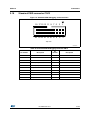
Figure 5. Motor control connector CN1
5PQWJFX
.47
Table 19. Motor control connector CN1(1)
Description
Pin of
STM32F072VB
Emergency
STOP
PB12 (R20
mounted by default)
Emergency
STOP2
PA3 (to close SB4)
Emergency
STOP3
PA1 (to close SB1)
PWM-UH
Pin
number
of CN1
Pin
number
of CN1
Pin of
STM32F072VB
Description
1
2
GND
PE9
3
4
GND
PWM-UL
PE8
5
6
GND
PWM-VH
PE11
7
8
GND
PWM-VL
PE10
9
10
GND
PWM-WH
PE13
11
12
GND
PWM-WL
PE12
13
14
PA1 (R10 mounted
by default)
BUS VOLTAGE
PC3 (to close SB3) BUS VOLTAGE2
26/63
PHASE A
CURRENT
PA2
PHASE B
CURRENT
PC5 (R14 mounted
by default)
PHASE B
CURRENT2
PA3 (to close SB5)
15
16
GND
17
18
GND
DocID025744 Rev 1
UM1714
Connectors
Table 19. Motor control connector CN1(1) (continued)
Description
Pin of
STM32F072VB
Pin
number
of CN1
Pin
number
of CN1
Pin of
STM32F072VB
Description
PHASE C
CURRENT
PC4
19
20
GND
NTC BYPASS
RELAY
PE7
21
22
GND
DISSIPATIVE
BRAKE PWM
PB11
23
24
GND
25
26
27
28
3.3V power
+5V power
PFC SYNC2
PC8 (Always be
connected)
Heatsink
temperature
PC2
PFC SYNC1
PF3 (to close SB2)
PFC PWM
PC9
29
30
GND
Encoder A
PA6
31
32
GND
Encoder B
PA7
33
34
PB0
Encoder Index
1. The signals in the grey table cells are not connected by default.
3.2
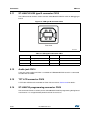
RF E2PROM connector CN2
Figure 6. RF EEPROM daughter board connector CN2
)URQWYLHZ
.47
Table 20. RF E2PROM connector CN2
Pin number
Description
Pin number
Description
1
I2C1_SDA (PB7)
5
+5V
2
NC
6
NC
3
I2C1_SCL (PB6)
7
GND
4
EX_RESET(PD7)
8
NC
DocID025744 Rev 1
27/63
62
Connectors
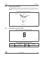
3.3
UM1714
HDMI sink connector CN3
Figure 7. HDMI Sink connectors CN3
'SPOUWJFX
.47
Table 21. HDMI Sink connectors CN3
Pin number
28/63
Description
Pin number
Description
1,3,4,6,7,9,10,12
TMDS differential signal pair
connected to CN5
16
I2C2_SDA (PB14)
13
CEC (PB8)
2,5,8,11,17
GND
14
NC
18
HDMI_5V_Sink
15
I2C2_SCL (PB13)
19
HPD (PD15 through transistor)
DocID025744 Rev 1
UM1714
3.4
Connectors
User USB type B connector CN4
Figure 8. USB type B connector CN4
'SPOUWJFX
.47
Table 22. USB type B connector CN4
Pin number
3.5
Description
Pin number
Description
1
VBUS(power)
4
GND
2
DM(PA11)
5,6
Shield
3
DP(PA12)
HDMI source connector CN5
Figure 9. HDMI source connectors CN5
)URQWYLHZ
069
DocID025744 Rev 1
29/63
62
Connectors
UM1714
Table 23. HDMI Source connectors CN5
Pin number
0.1
Description
Pin number
Description
1,3,4,6,7,9,10,12
TMDS differential signal pair
connected to CN3
16
I2C1_SDA (PB7)
13
CEC (PB8)
2,5,8,11,17
GND
14
NC
18
HDMI_5V_Source from power
switch U3
15
I2C1_SCL (PB6)
19
HPD (PE0)
CAN D-type and 9-pin male connector CN6
Figure 10. CAN D-type and 9-pin male connector CN6
'SPOUWJFX
.47
Table 24. CAN D-type and 9-pin male connector CN6
3.6
Pin number
Description
Pin
number
Description
1,4,8,9
NC
7
CANH
2
CANL
3,5,6
GND
Daughter board extension connector CN7 and CN8
Two 52-pin male headers CN7 and CN8 can be used to connect with the daughter board or
with the standard wrapping board to STM32072B-EVAL evaluation board. All GPI/Os are
available on the connector. The space between these two connectors and position of power,
GND and RESET pin are defined as a standard, allowing the development of common
daughter boards for several evaluation boards. The standard width between CN7 pin1 and
CN8 pin1 is 2700mils (68.58mm). The standard was implemented on the majority of
evaluation boards.
30/63
DocID025744 Rev 1
UM1714
Connectors
Each pin on CN7 and CN8 can be used by a daughter board after disconnecting it from the
corresponding function block on STM32072B-EVAL evaluation board. Please look at
Table 25 and Table 26 for details.
Table 25. Daughter board extension connector CN7
Pin
Description
Alternative function
How to disconnect with function block on
STM32072B-EVAL board
1
GND
-
-
3
PC7
-
-
5
PC9
MC_PFCpwm
Disconnect MC power board from CN1
7
PA9
SmartCard_IO
Remove R152
9
PA10
SmartCard_RST
Remove R155
11
PC14
OSC32_IN
Remove R71, Close SB14
13
PA12
USB_DP
Remove R34
15
PC15
OSC32_OUT
Remove R72, Close SB15
17
PA14
SWCLK /
USART2_TX_BOOT
Keep JP2, JP10 open
19
GND
-
-
21
PC11
SmartCard_3/5V
Remove R184
23
PD0
CAN_RX
Remove R47
25
PD2
SmartCard_CMDVCC
Remove R156
27
PD4
USART2_RTS/RS485_DIR
Remove R65
29
PD6
USART2_RX
Keep JP7 open
31
PD7
EX_RESET
Remove R28
33
PB4
-
-
35
PB6
I2C1_SCL
Remove R5,R7,R41,R42
37
PB8
HDMI_CEC
Remove R27
39
GND
-
-
41
PE1
-
-
43
PE3
JOY_RIGHT
Remove R202
45
PF9
JOY_UP
Remove R200
47
PF10
JOY_DOWN
Remove R197
49
PC1
Audio_IN
Remove R129
51
PE5
SHIELD_CT
Remove R67, Close SB18
2
PD15
HDMI_HPD_SINK
Remove R23
4
PC6
IR_IN
Remove R175
6
PC8
MC_PFCsync2
Disconnect MC power board from CN1, Keep
SB2 open
8
PA8
SmartCard_CK
Remove R153
DocID025744 Rev 1
31/63
62
Connectors
UM1714
Table 25. Daughter board extension connector CN7 (continued)
Pin
Description
Alternative function
How to disconnect with function block on
STM32072B-EVAL board
10
GND
-
-
12
PA11
USB_DM
Remove R35
14
PA13
SWDAT
Remove R76
16
PF6
-
-
18
PA15
USART2_RX_BOOT
Keep JP7 open
20
PC10
SmartCard_1.8V
Remove R159
22
PC12
SmartCard_OFF
Remove R154
24
PD1
CAN_TX
Remove R54
26
PD3
USART2_CTS
Remove R87
28
PD5
USART2_TX
Remove R69
30
GND
-
-
32
PB3
SPI1_SCK
Remove R95
34
PB5
TempSensor_INT
Remove R4
36
PB7
I2C1_SDA
Remove R2,R6,R44,R45
38
PB9
IR_OUT
Remove R135
40
PE0
HDMI_HPD_Source
Remove R49
42
PE2
JOY_LEFT
Remove R199
44
PE6
LCD_CS
Remove R113
46
PC0
Potentiometer
Remove R204
48
+3V3
-
-
50
GND
-
-
52
PE4
SHIELD
Remove R66, Close SB19
Table 26. Daughter board extension connector CN8
Pin
32/63
Description
Alternative Function
How to disconnect with function block on
STM32072B-EVAL board
1
GND
-
-
3
PD14
TS_CT
Remove C17, Close SB11
5
PD13
TS2
Remove R39, Close SB12
7
PD12
TS1
Remove R40, Close SB13
9
PC13
TAMPER_KEY
Remove R194
11
RESET#
-
-
13
PB13
I2C2_SCL
Remove R30
15
PB11
MC_Dissipativebrake
Disconnect MC power board from CN1
DocID025744 Rev 1
UM1714
Connectors
Table 26. Daughter board extension connector CN8 (continued)
Pin
Description
Alternative Function
How to disconnect with function block on
STM32072B-EVAL board
17
PE15
SPI1_MOSI
Remove R104
19
D5V
-
-
21
PE12
MC_WL
Disconnect MC power board from CN1
23
PF0
OSC_IN
Remove X2,C31, Close SB16
25
PE11
MC_VH
Disconnect MC power board from CN1
27
PE10
MC_VL
Disconnect MC power board from CN1
29
PE8
MC_UL
Disconnect MC power board from CN1
31
PB2
SPI1_MOSI_DIR
Remove R102
33
PB0
MC_Enindex
Disconnect MC power board from CN1
35
PC5
MC_Current B
Remove R14
37
PA7
MC_Encoder B
Disconnect MC power board from CN1
39
GND
-
-
41
PA4
Audio_OUT_LEFT
Keep JP18 open
43
VDD_IO2
-
-
45
PA2
MC_Current A
Remove R16
47
PA0
JOY_SEL
Remove R198
49
PF2
MicroSD_CS
Remove R74
51
PC2
MC_headsinkTemp
Remove R11
2
PD11
LED4
Remove R176
4
PD10
LED3
Remove R177
6
PD9
LED2
Remove R178
8
PD8
LED1
Remove R179
10
GND
-
-
12
PB15
SDcard_detect
Remove R56
14
PB14
I2C2_SDA
Remove R32
16
PB12
MC_EmergencySTOP
Remove R20
18
PB10
USB_VBUS_detection
Remove R50,R53
20
PE14
SPI1_MISO
Remove R58
22
PE13
MC_WH
Disconnect MC power board from CN1
24
VDD
-
-
26
PF1
OSC_OUT
Remove R73, Close SB17
28
PE9
MC_UH
Disconnect MC power board from CN1
30
GND
-
-
32
PE7
MC_ NTC
Disconnect MC power board from CN1
DocID025744 Rev 1
33/63
62
Connectors
UM1714
Table 26. Daughter board extension connector CN8 (continued)
Pin
3.7
Description
How to disconnect with function block on
STM32072B-EVAL board
Alternative Function
34
PB1
-
-
36
PC4
MC_Current C
Remove R13
38
PA6
MC_Encoder A
Keep JP1 open, Disconnect MC power board
from CN1
40
PA5
Aduio_OUT_RIGHT
Keep JP18 open
42
NC
-
-
44
PA3
MC_Current B2/
MC_Emergency_STOP2
Keep SB4,SB5 open
46
PA1
LDR_IN/MC_BusVoltage /
MC_Emergency_STOP3
Keep JP6 open
48
PF3
MC_PFCsync1
Keep SB2 open
50
GND
-
-
52
PC3
MC_BusVoltage2
Keep SB3 open
MicroSD connector CN9
Figure 11. MicroSD connector CN9
'SPOUWJFX
.47
Table 27. MicroSD connector CN9
Pin number
34/63
Pin
number
Description
Description
1
NC
5
MicroSDcard_CLK (PB3)
2
MicroSDcard_CS (PF2)
6
Vss/GND
3
MicroSDcard_DIN(PE15)
7
MicroSDcard_DOUT(PE14)
DocID025744 Rev 1
UM1714
Connectors
Table 27. MicroSD connector CN9 (continued)
Pin number
4
3.8
Pin
number
Description
+3V3
Description
8
NC
10
MicroSDcard_detect (PB15)
RS232 and RS485 connector CN10
Figure 12. RS232 and RS485 connector CN10
'SPOUWJFX
.47
Table 28. RS232 and RS485 connector CN10
Pin number
Pin
number
Description
Description
1
NC
6
Bootloader_BOOT0
2
RS232_RX
(PD6 or PA15)
7
RS232_RTS(PD4)
3
RS232_TX
(PD5 or PA14)
8
RS232_CTS(PD3)/Bootloader_RESET
4
RS485_A
9
RS485_B
5
GND
DocID025744 Rev 1
35/63
62
Connectors
3.9
UM1714
High-density SWD connector CN11
Figure 13. High-density SWD debugging connector CN11
5PQWJFX
.47
Table 29. High-density SWD debugging connector CN11
Pin number
36/63
Pin
number
Description
Description
1
VDDIO2
2
SWDAT(PA13)
3
GND
4
SWCLK(PA14)
5
GND
6
NC
7
KEY
8
NC
9
GND
10
RESET#
DocID025744 Rev 1
UM1714
3.10
Connectors
Standard SWD connector CN12
Figure 14. Standard SWD debugging connector CN12
5PQWJFX
.47
Table 30. Standard SWD debugging connector CN12
Pin number
Pin
number
Description
Description
1
VDDIO2
2
VDDIO2
3
NC
4
GND
5
NC
6
GND
7
SWDAT(PA13)
8
GND
9
SWCLK(PA14)
10
GND
11
10K pull-down
12
GND
13
NC
14
GND
15
RESET#
16
GND
17
10K pull-down
18
GND
19
10K pull-down
20
GND
DocID025744 Rev 1
37/63
62
Connectors
3.11
UM1714
ST-LINK/V2 USB type B connector CN13
The USB connector CN13 is used to connect embedded ST-LINK/V2 to PC for debugging of
board.
Figure 15. USB type B connector CN13
)URQWYLHZ
069
Table 31. USB type B connector CN13
Pin number
3.12
Description
Pin number
Description
1
VBUS(power)
4
GND
2
DM
5,6
Shield
3
DP
Audio jack CN14
A 3.5 mm stereo audio jack CN14 is available on STM32072B-EVAL board. It is connected
to audio DAC and ADC.
3.13
TFT LCD connector CN15
A TFT color LCD board is mounted on CN15. Please refer to Section 2.20 for details.
3.14
ST-LINK/V2 programming connector CN16
The connector CN16 is used only for the embedded ST-LINK/V2 programming during board
manufacture. It is not populated by default and not for end users.
38/63
DocID025744 Rev 1
UM1714
3.15
Connectors
Power connector CN17
The STM32072B-EVAL evaluation board can be powered from a DC 5V power supply via
the external power supply jack (CN17) shown in Figure 16. The central pin of CN17 must be
positive.
Figure 16. Power supply connector CN17
'&9 *1' )URQWYLHZ
.47
3.16
Analog input connector CN18
Figure 17. Analog input-output connector CN18
ϭ
Ϯ
Eϭϴ
5PQWJFX
.47
Table 32. Analog input-output connector CN18
Pin number
1
Pin
number
Description
Analog input-output PC0
DocID025744 Rev 1
2
Description
GND
39/63
62
Connectors
3.17
UM1714
Smart card connector CN19
Figure 18. Smart card connector CN19
5PQWJFX
.47
Table 33. Smart card connector CN19
Pin number
40/63
Description
Pin
number
Description
1
VCC
5
GND
2
RST
6
NC
3
CLK
7
I/O
4
NC
8
NC
17
Detection pin of card presence
18
Detection pin of card presence
DocID025744 Rev 1
UM1714
4
Schematics
Schematics
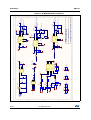
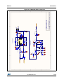
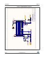
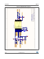
The schematics of STM32072B-EVAL are shown in the Figure 19 to Figure 32.
The schematic of the TFT LCD daughter board is shown in Figure 33.
DocID025744 Rev 1
41/63
62
42/63
DocID025744 Rev 1
D
C
B
A
1
1
Audio_OUT_L
Audio_OUT_R
Audio_IN
2
SHIELD
SHIELD_CT
TS1
TS2
TS_CT
DB_PD12
DB_PD13
DB_PD14
DB_PE4
DB_PE5
USB_DP
USB_DM
Potentiometer
LDR_OUT
Tamper_key
JOY_SEL
JOY_UP
JOY_DOWN
JOY_LEFT
JOY_RIGHT
LED1
LED2
LED3
LED4
U_Touch Sensing
Touch Sensing.SchDoc
U_Peripherals
Peripherals.SchDoc
I2C1_SCL_5V
I2C1_SDA_5V
TempSensor_INT
EX_RESET
U_TemSensor_RF_EEPROM
TemSensor_RF_EEPROM.SCHDOC
HDMI_HPD_Source_5V
I2C1_SCL_5V
I2C1_SDA_5V
HDMI_HPD_SINK
I2C2_SCL_5V
I2C2_SDA_5V
HDMI_CEC_3V3
U_HDMI_CEC
HDMI_CEC.SchDoc
CAN_RX
CAN_TX
IR_OUT
IR_IN
SmartCard_IO
SmartCard_CLK
SmartCard_RST
SmartCard_OFF
SmartCard_3/5V
SmartCard_CMDVCC
SmartCard_1V8
U_CAN_SmartCard_IR
CAN_SmartCard_IR.SchDoc
U_Audio
Audio.SchDoc
2
3
3
SHIELD
SHIELD_CT
TS1
TS2
TS_CT
DB_PD12
DB_PD13
DB_PD14
DB_PE4
DB_PE5
USB_DP
USB_DM
Potentiometer
LDR_OUT
Tamper_key
JOY_SEL
JOY_UP
JOY_DOWN
JOY_LEFT
JOY_RIGHT
LED1
LED2
LED3
LED4
TempSensor_INT
EX_RESET_OD
HDMI_HPD_Source
I2C1_SCL
I2C1_SDA
HDMI_HPD_SINK_OD
I2C2_SCL
I2C2_SDA
HDMI_CEC_OD
CAN_RX
CAN_TX
IR_OUT
IR_IN
SmartCard_IO
SmartCard_CLK
SmartCard_RST
SmartCard_OFF
SmartCard_3/5V
SmartCard_CMDVCC
SmartCard_1V8
Audio_OUT_L
Audio_OUT_R
Audio_IN
U_MCU
MCU.SchDoc
4
VDD_IO2
100K
R146
USART2_RX
USART2_RX_BOOT
USART2_TX
USART2_TX_BOOT
USART2_RTS
USART2_CTS
Bootloader_BOOT0
Bootloader_RESET
SWCLK
SWDAT
SPI1_SCK
SPI1_MOSI
SPI1_MOSI_DIR
SPI1_MISO
MicroSD_CS_OD
LCD_CS_OD
SDcard_detect
RESET#
MC_CurrentB2
MC_PFCsync1
MC_PFCsync2
MC_UL
MC_UH
MC_VL
MC_VH
MC_WL
MC_WH
MC_NTC
MC_DissipativeBrake
MC_PFCpwm
MC_EmergencySTOP
MC_CurrentA
MC_CurrentB
MC_CurrentC
MC_EnA
MC_EnB
MC_EnIndex
MC_HeatsinkTemperature
MC_BusVoltage2
MC_BusVoltage
4
VDD_IO2
U16
VccB VccA
B1
A1
B2
A2
DIR GND
1
2
3
4
C78
100nF
+3V3
5
SN74LVC2T45DCUT
8
7
6
5
C80
100nF
1Mhz clock
24Mhz clock
5
6
USART2_RX_3V3
USART2_RX_BOOT_3V3
USART2_TX
USART2_TX_BOOT_3V3
USART2_RTS
USART2_CTS_3V3
Bootloader_BOOT0_3V3
Bootloader_RESET_3V3
U_RS232_RS485_IrDA
RS232_RS485_IrDA.SchDoc
TCK/SWCLK
TMS/SWDIO
RESET#
T_SWDIO_IN
U_ST_LINK_V2
ST_LINK_V2.SCHDOC
SWCLK
SWDAT
RESET#
U_SWD
SWD.SchDoc
SPI1_SCK
SPI1_MOSI
SPI1_MOSI_DIR
SPI1_MISO_3V3
MicroSD_CS_3V3
LCD_CS_3V3
SDcard_detect
RESET#
U_LCD_MicroSD
LCD_MicroSD.SchDoc
MC_PFCsync1
MC_PFCsync2
MC_UL
MC_UH
MC_VL
MC_VH
MC_WL
MC_WH
MC_NTC
MC_DissipativeBrake
MC_PFCpwm
MC_EmergencySTOP
MC_CurrentA
MC_CurrentB
MC_CurrentC
MC_EnA
MC_EnB
MC_EnIndex
MC_HeatsinkTemperature
MC_BusVoltage2
MC_BusVoltage
MC_EmergencySTOP3
MC_CurrentB2
MC_EmergencySTOP2
U_MotorCtrl
MotorCtrl.SchDoc
6
8
7
Rev: B.1[PCB.SCH]
STM32072B-EVAL
Number:MB1070
Title:
Date: 10/9/2013
STMicroelectronics
8
Sheet
1 of
14
Note1:The signals which was marked in red should be routed firstly with shield during
PCB layout.
Note2: Text in italic placed on a wire doesn’ t correspond to net name. It just helps to
identify rapidly MCU IO related to this wire.
Note3:VDDIO2 is connected to Pin43 of CN8 from Version A.1 to B.1
Note4:TP13 is added to ground from Version A.1 to B.1
Note5:Pressure sensor circuits are removed from Version A.1 to B.1
Note6:ESD protection component D10 on CAN was added from Version A.1 to B.1
Note7:PF4 & PF5 signals are removed on CN8 from Version A.1 to B.1
Note8:Value of R66 was changed to 1K ohm from Version A.1 to B.1
Note9:Remove D5 & D6 by default from Version A.1 to B.1
U_Power
Power.SchDoc
7
D
C
B
A
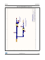
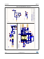
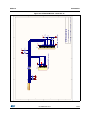
Schematics
UM1714
Figure 19. STM32072B-EVAL schematic 1
D
C
B
LDR_OUT
3
2
MC_DissipativeBrake
MC_EmergencySTOP
I2C2_SCL
I2C2_SDA
SDcard_detect
TempSensor_INT
I2C1_SCL
I2C1_SDA
HDMI_CEC_OD
IR_OUT
PB3 R207
MC_EnIndex
R73
0
4
1
100nF
C114
3
B1
TD-0341 [RESET/Black]
1
2
RESET#
20pF
C32
VDD
10
11
14
94
PF9
PF10
RESET#
BOOT0
JP15
PE15
PE14
PE13
PE12
PE11
PE10
PE9
PE8
PE7
PE6
PE5
PE4
PE3
PE2
PE1
PE0
PD15
PD14
PD13
PD12
PD11
PD10
PD9
PD8
PD7
PD6
PD5
PD4
PD3
PD2
PD1
PD0
46
45
44
43
42
41
40
39
38
5
4
3
2
1
98
97
62
61
60
59
58
57
56
55
88
87
86
85
84
83
82
81
9
8
7
80
79
78
66
65
64
63
34
33
18
17
16
15
2
Bootloader_RESET
Bootloader_BOOT0
STM32F072VBT6
BOOT0
NRST
PF9
PF10
PF6
PF0-OSC_IN
PF1-OSC_OUT
PF2
PF3
PB0
PB1
PB2
PB3
PB4
PB5
PB6
PB7
PB8
PB9
PB10
PB11
PB12
PB13
PB14
PB15
BAT60JFILM
D4
2
PA0 PC15-OSC32_OUT
PA1
PC14-OSC32_IN
PA2
PC13
PA3
PC12
PA4
PC11
PA5
PC10
PA6
PC9
PA7
PC8
PA8
PC7
PA9
PC6
PA10
PC5
PA11
PC4
PA12
PC3
PA13
PC2
PA14
PC1
PA15
PC0
U4A
BAT60JFILM
D2
73
PF6
JP5
12
13
19
22
PB4
PB5
PB6
PB7
PB8
PB9
PB10
PB11
PB12
PB13
PB14
PB15
35
36
37
89
90
91
92
93
95
96
47
48
51
52
53
54
PB0
PB1
PB2
PF0
PF1
PF2
PF3
0
23
24
25
26
29
30
31
32
67
68
69
70
71
72
76
77
PA0
PA1
PA2
PA3
PA4
PA5
PA6
PA7
PA8
PA9
PA10
PA11
PA12
PA13
PA14
PA15
SW1
09.03290.01
R59
10K
JOY_UP
JOY_DOWN
X2
ESA8.00000F20D25F(with socket)
C31
20pF
MicroSD_CS_OD
MC_PFCsync1
R50
82K
R53
47K
JOY_SEL
MC_CurrentA
MC_CurrentB2
Audio_OUT_L
Audio_OUT_R
MC_EnA
MC_EnB
SmartCard_CLK
SmartCard_IO
SmartCard_RST
USB_DM
USB_DP
SWDAT
USART2_RX_BOOT
SPI1_MOSI_DIR
SPI1_SCK
U5V
USART2_TX_BOOT
JP2
SWCLK
MC_BusVoltage
2
A
JP6
1
1
DocID025744 Rev 1
3
PE14
PE13
PE12
PE11
PE10
PE9
PE8
PE7
PE6
PE5
PE4
PE3
PE2
PE1
PE0
PD15
PD14
PD13
PD12
PD11
PD10
PD9
PD8
PD7
PD6
PD5
PD4
PD3
PD2
PD1
PD0
PC15
PC14
PC13
PC12
PC11
PC10
PC9
PC8
PC7
PC6
PC5
PC4
PC3
PC2
PC1
PC0
0
0
PE15
HDMI_HPD_Source
SPI1_MISO
MC_WH
MC_WL
MC_VH
MC_VL
MC_UH
MC_UL
MC_NTC
LCD_CS_OD
SHIELD_CT
SHIELD
JOY_RIGHT
JOY_LEFT
0
C29
20pF
3
20pF
3
PF1
PF0
SB15
SB14
PA2
PA0
PF2
PC2
PA4
PE11
PE10
PE8
PB2
PB0
PC5
PA7
D5V
PE12
R37
R38
PB13
PB11
PE15
PE1
PE3
PF9
PF10
PC1
PC11
PD0
PD2
PD4
PD6
PD7
PB4
PB6
PB8
PA14
PA12
PC7
PC9
PA9
PA10
820
820
Rev: B.1(PCB.SCH)
STM32072B-EVAL MCU
Number:MB1070
Title:
Right
2
4
6
8
10
12
14
16
18
20
22
24
26
28
30
32
34
36
38
40
42
44
46
48
50
52
2213S-52G
1
3
5
7
9
11
13
15
17
19
21
23
25
27
29
31
33
35
37
39
41
43
45
47
49
51
CN8
4
Left
2
4
6
8
10
12
14
16
18
20
22
24
26
28
30
32
34
36
38
40
42
44
46
48
50
52
2213S-52G
1
3
5
7
9
11
13
15
17
19
21
23
25
27
29
31
33
35
37
39
41
43
45
47
49
51
Extension connector
CN7
4
Date: 10/9/2013
STMicroelectronics
SB17
SB16
VDD_IO2
DB_PD14
DB_PD13
DB_PD12
DB_PE5
Open by default
PC13
RESET#
PC15
PC14
X1
Q13MC3061000300(EPSON 12.5pF)
SPI1_MOSI
HDMI_HPD_SINK_OD
TS_CT
TS2
TS1
LED4
LED3
LED2
LED1
EX_RESET_OD
USART2_RX
USART2_TX
USART2_RTS
USART2_CTS
SmartCard_CMDVCC
CAN_TX
CAN_RX
R208
C30
4
1
IR_IN
MC_CurrentB
MC_CurrentC
MC_BusVoltage2
MC_HeatsinkTemperature
Audio_IN
Potentiometer
Tamper_key
SmartCard_OFF
SmartCard_3/5V
SmartCard_1V8
MC_PFCpwm
MC_PFCsync2
R71
R72
3
2
1
Sheet
PC3
PA3
PA1
PF3
PE7
PB1
PC4
PA6
PA5
PE9
PB15
PB14
PB12
PB10
PE14
PE13
PD11
PD10
PD9
PD8
+3V3
PB3
PB5
PB7
PB9
PE0
PE2
PE6
PC0
PA11
PA13
PF6
PA15
PC10
PC12
PD1
PD3
PD5
PD15
PC6
PC8
PA8
2 of
VDD
DB_PE4
14
D
C
B
A
UM1714
Schematics
Figure 20. STM32072B-EVAL MCU schematic 2
43/63
62
D
C
B
A
1
+3V3
U5V
U5V_ST_LINK
D5V
E5V
4
C22
100nF
1
3
1
2
C23
100nF
7
5
3
1
VDD
Header 4X2
8
6
4
2
JP19
3
1
JP8
2
C18
100nF
C19
4.7uF
C16
1uF
C15
100nF
TP1
VDDA VDDA
CV
SG CG1
CG2
CG3
SV
1K
6
21
75
100
50
28
2
4
5
6
3
VSSA
VSS
VSS
VSS
VSS
TP12
Ground
20
74
99
49
27
TP13
Ground
C89
220uF
E5V
2
C27
1uF
VDDA
JP11
C24
10nF
STM32F072VBT6
BT1 CR1220 holder
3
2
1
VDD
VBAT
VDDA
VDDIO2
VDD1
VDD2
VDD3
U4B
LD7
red
1
BNX002-01
R96
2
1
VDD_MCU
TP7
5V
C104
100nF
VDD_MCU2
VDD_MCU2
BEAD
JP9
L1
BAT60JFILM
D3
JP16
JP12
+5V
Z1
SMAJ5.0A-TR
TP4
VDD_IO2
VDD_IO2
TP2
VDD
JP14
JP13
2
3
VDD_ANA
2
VDD_MCU
+3V3
VDD_MCU
+3V3_IO2
VDD
VDD_ADJ
DC-10B
1
2
3
L2
+3V3_PG
VDD_PG
R99
0
R106
C55
[N/A]
+5V
0
C57
[N/A]
+5V
C46
4.7uF
+5V
3
1
6
3
EN
VI
C49
4.7uF
1
6
VO
PG
3
5
4
5
4
ADJ
VO
PG
5
4
3
11.8K[1%]
R86
C45
R88
Rev: B.1(PCB.SCH)
C38
10uF[ESR<0.2ohm]
4
Date: 10/9/2013
C51
100nF
TP5
+3V3_IO2
+3V3_IO2
Sheet
3 of
C50
10uF[ESR<0.2ohm]
14
Power Supply 3.3V
Vout=1.22*(1+R1/R2)
C48
10uF[ESR<0.2ohm]
[N/A]
STM32072B-EVAL Power
Number:MB1070
Title:
VDD_ADJ
+3V3
Power Supply 3.3V
Vout=1.22*(1+R1/R2)
Power Supply VDD_ADJ [1.65V to 3.5V]
considering potentiometer error tolerance
Vout=1.22*(1+R1/R2)
20.5K[1%]
C47
100nF
RV2
23386P-503H[5%]
[N/A]
C43
4
TP3
+3V3
C37
100nF
TP6
VDD_ADJ
[N/A]
R84
22.1K[1%]
11.8K[1%]
R79
C41
+5V
20.5K[1%]
+3V3_PG
[N/A]
R80
VDD_PG
R100
[N/A]
+5V
ADJ
VO
PG
3
R82
STMicroelectronics
EN
VI
U10
ST1L05BPUR
R81
11.8K[1%]
ADJ
EN
VI
U7
ST1L05BPUR
U9
ST1L05BPUR
C44
4.7uF
1
6
GND
U21
ZEN056V130A24LS
2
GND
2
GND
7
GND
2
CN17
3
1
1
3
7
GND
2
DocID025744 Rev 1
GND
44/63
7
1
D
C
B
A
Schematics
UM1714
Figure 21. STM32072B-EVAL schematic 3
DocID025744 Rev 1
D
C
B
1
Audio_OUT_R
Audio_OUT_L
PA5
PA4
JP18
1
2
3
100
R121
10uF
C72
100nF
C67
C70
4.7uF
15K
R125
100K
R122
100K
R119
JP20
C63
2.2uF
R115
18K
2
C65
4.7uF
R116
680
R165
20K
330nF
C94
Shutdown VOUT1
VIN1
VOUT2
VIN2
VCC
Bypass
GND
4K7
4K7
1.5nF
R162
TS488IQT
C79
1uF
C88
6
3
7
4
U17
1.5nF
R147
C82
2
4
100nF
3
C69
180pF
R117 82K
C64
U15
TS461CLT
1
VDD_ANA
2
8
1
5
9
VDD_ANA>2.2V
VDD_ANA>2.7V
RV1
[N/A]
R128
10K
R144
20K
330nF
C75
TP10
MIC+
C91
[N/A]
C74
[N/A]
VDD_ANA
C68
47pF
R126
2K2
R131
1K
VDD_ANA
0
R161
0
R143
Default setting: close
VDD_ANA
2
1
3
5
2
A
1
R120
0
C86
1uF
VDD_ANA
R142
1K
3
C71
[N/A]
4
2
R129
0
510
R160
1K
Audio_IN
Rev: B.1(PCB.SCH)
STM32072B-EVAL Audio
Number:MB1070
Title:
4
4
Date: 10/9/2013
STMicroelectronics
PC1
PJ3028B-3
3 CN14
6
Microphone
Left
Right
R130
TP11
MIC_OUT
220uF
C90
C85
100nF
220uF
C77
3
Sheet
4 of
14
D
C
B
A
UM1714
Schematics
Figure 22. STM32072B-EVAL schematic 4
45/63
62
DocID025744 Rev 1
D
C
B
A
HDMI_HPD_SINK
2
1
Open drain pin!
I2C2_SCL_5V
I2C2_SDA_5V
HDMI_CEC_3V3
PB13
PB14
PB8
R30
R32
R27
CN3
Sink
47151-0051
0
0
0
R33
1K
T1
9012
HDMI_5V_Sink
FT pin & Open Drain mode needed
PD15
R23
1K
1K
R26
1
3
21
20
1
2
3
4
5
6
7
8
9
10
11
12
13
14
15
16
17
18
19
2
+5V
HDMI_5V_Sink
R31 R29
47K 47K
22
23
2
2
D
27K
+5V
+3V3
TMDS_Clock-
TMDS_Data0TMDS_Clock+
TMDS_Data1TMDS_Data0+
TMDS_Data2TMDS_Data1+
TMDS_Data2+
T2
2N7002
R24
S
SB9
SB10
SB7
SB8
2
5
4
3
1
R51
1M
STMPS2141STR@54
GND FAULT
IN
OUT
EN
U3
3
3
R41
R45
R48
C21 0
4.7uF
1
2
3
4
5
6
7
8
9
10
11
12
13
14
15
16
17
18
19
0
0
R49
PE0
PB6
PB7
I2C1_SCL_5V
I2C1_SDA_5V
HDMI_HPD_Source_5V
Rev: B.1(PCB.SCH)
4
4
Date: 10/9/2013
STM32072B-EVAL HDMI_CEC
Number:MB1070
Title:
STMicroelectronics
R44 R42
1K8 1K8
+5V
0
47151-0051
CN5
Source
HDMI_5V_Source
21
20
22
23
46/63
3
1
1
Sheet
5 of
14
D
C
B
A
Schematics
UM1714
Figure 23. STM32072B-EVAL schematic 5
G
DocID025744 Rev 1
D
C
B
A
SPI1_SCK
SPI1_MOSI_DIR
VDD
SPI1_MOSI
1
PB3
R102
PB2
0
R94
100K
VDD
+3V3
8
7
6
5
SN74LVC2T45DCUTVDD
+3V3
8
7
6
5
SN74LVC2T45DCUT
C53
VDD U11
1
100nF
VCCA VCCB
R95
0
2
A1
B1
3
A2
B2
4
GND
DIR
10K
R107
PE15
R104
C58
VDD U13
1
100nF
VCCA VCCB
2
A1
B1
3
0
A2
B2
4
GND
DIR
C52
100nF
C59
100nF
2
SPI1_SCK_3V3
SPI1_MOSI_3V3
2
PF2
RESET#
+5V
+3V3
LCD_CS_3V3
R169
R182
S
10K
R62
D
R123
4K7
3
BEAD
BEAD
L4
L3
3
+3V3
R112
10K
+3V3
0
3
R68
10K
+3V3
0
TR1
BSN20
0
[N/A]
1
G
VDD
R113
R74
SPI1_MOSI_3V3
R58
0
SPI1_SCK_3V3
PE6
PE14
Open drain pin!
Open drain pin!
MicroSD_CS_3V3
SPI1_MISO_3V3
2
1
270
C95
100nF
R127
+3V3
SW1
SW2
9
10
11
12
13
14
15
16
1
2
3
4
5
6
7
8
10
9
0
SPI LCD
TFT LCD
VDD
VCI
GND
GND
BL_VDD
BL_Control
BL_GND
BL_GND
CS
SCL
SDI
RS
WR
RD
SDO
RESET
Rev: B.1(PCB.SCH)
4
Date: 10/9/2013
Sheet
R56
CN15
2.4" LCD connector (MB895C)
SPI MICRO SD
STM32072B-EVAL LCD & Micro SD card
Number:MB1070
Title:
PB15
PJS008-2000 (SMS064FF or SMS128FF)
RVS
DO
Vss
SCLK
Vdd
DI
CS
RVS
CN9
STMicroelectronics
C96
10uF
R63
270
+3V3
8
7
6
5
4
3
2
1
SDcard_detect
Input pin with pull-up
4
6 of
14
D
C
B
A
UM1714
Schematics
Figure 24. STM32072B-EVAL schematic 6
47/63
62
48/63
DocID025744 Rev 1
D
C
B
A
MC_CurrentB2
MC_CurrentB
PA1
PA3
PB12
1
0
R14 0
MC_PFCsync1
MC_PFCsync2
PC4
PA2
PF3
PC8
0
R21
SB2 Open by default
R13 0
C6
[N/A]
R15 0
C7
[N/A]
R16 0
C8
[N/A]
SB1 Open by default
C10
1nF
R19
3.3K
+3V3
SB4 Open by default
R20
SB5
Open by default
MC_CurrentC
PA3
PC5
MC_CurrentA
MC_EmergencySTOP3
MC_EmergencySTOP2
MC_EmergencySTOP
1
C4
[N/A]
2
MC_PFCpwm
MC_EnA
MC_EnB
MC_NTC
MC_DissipativeBrake
MC_UH
MC_UL
MC_VH
MC_VL
MC_WH
MC_WL
2
PC9
PA6
PA7
+5V
PE7
PB11
PE9
PE8
PE11
PE10
PE13
PE12
C12
10nF
JP1
MC_connector
EMERGENCY STOP
MC-UH
MC_UL
MC_VH
MC_VL
MC_WH
MC_WL
CURRENT A
CURRENT B
CURRENT C
NTC BYPASS RELAY
DISSIPATIVE BRAKE
+5V POWER
PFC SYNC
PFC PWM
Encoder A
Encoder B
CN1
C3
[N/A]
C1
[N/A]
Default setting: Open
1
3
5
7
9
11
13
15
17
19
21
23
25
27
29
31
33
Motor control connector
3
GND
GND
GND
GND
GND
GND
BUS VOLTAGE
GND
GND
GND
GND
GND
Heatsink Temperature
3.3V Power
GND
GND
Encoder Index
3
+3V3
0
R17
0
R12
R11
PB0
C2
[N/A]
PC2
Rev: B.1(PCB.SCH)
PA1
4
MC_BusVoltage2
MC_BusVoltage
Sheet
7 of
MC_HeatsinkTemperature
Date: 10/9/2013
STM32072B-EVAL Motor control
Number:MB1070
Title:
0
PC3
Open by default
R10
MC_EnIndex
R18
100K SB3
0
C5
100nF
C9
100nF
STMicroelectronics
2
4
6
8
10
12
14
16
18
20
22
24
26
28
30
32
34
4
14
D
C
B
A
Schematics
UM1714
Figure 25. STM32072B-EVAL schematic 7
D
C
B
PA1
1
R205 47
PA0
PF10
PE2
PE3
PF9
0
0
0
0
0
8K2
R1
VT9ON1
0
VDD
R203 0
R8
R198
R197
R199
R202
R200
Close to MCU on PCB
C113
[N/A]
R206 0
R9
0
R204
Input pins with pull-down
JOY_SEL
JOY_DOWN
JOY_LEFT
JOY_RIGHT
JOY_UP
LDR_OUT
PC0
100nF
C108
Potentiometer
100nF
C107
RV3
10K
100
R201
VDD_ANA
2
C112
100nF
2
3
1
4
6
2
5
2
MT-008A
DWON
LEFT
RIGHT
UP
Selection
COMMON
B3
Photo resistor
Potentiometer
VDD_ANA
1
3
A
CN18
100nF
C109
LD4
Blue
1
LD3
Red
1
Joystick
GND
GND
680
R190
680
R191
680
R192
510
R193
7
8
PC13 R194
0
2
2
LD2
Orange
1
2
LD1
Green
1
2
Tamper_key
+3V3
2
0
0
0
R178
R177
R176
VCC
DD+
GND
SHELL
SHELL
CN4
LED4
LED3
LED2
LED1
1
2
3
4
6
5
R36
C14 1M
4.7nF
U5V
3
LEDs
3
R174
0
1.54K[1%]
R187
1K[1%]
R173
1
2
3
R171
0
R186
2.67K[1%]
6
6
5
4
+3V3
VDD_ANA<2.4V
R35
R34
C13
100nF
TS3702IPT
Rev: B.1(PCB.SCH)
4
Date: 10/9/2013
STM32072B-EVAL Peripherals
Number:MB1070
Title:
0
0
7
+3V3
1
2
LD5
Red
LD6
Orange
Sheet
PA11
PA12
8 of
USB
USB_DM
USB_DP
14
Low Voltage LED
R188
510
+3V3
MCU not functional
R189
510
1
VDD<2V
4
Analogue not functional
STMicroelectronics
USBLC6-2P6
I/O1
I/O1
GND Vbus
I/O2
I/O2
D1
2
U20A
3
TS3702IPT
VDD
R172
VDD_ANA U20B
1K[1%]
5
+3V3
+3V3
Optional only to increase ESD immunity level
U5V
Tamper Button
C106
100nF
PD11
PD10
PD9
PD8
VDD_IO2>3V
100
R196
B2
Tamper
R195
4K7
VDD
0
R179
USB-typeB connector
1
8
4
two pin header for external analog input
100nF
100nF
C111
DocID025744 Rev 1
C110
3
4
1
2
1
D
C
B
A
UM1714
Schematics
Figure 26. STM32072B-EVAL schematic 8
49/63
62
50/63
DocID025744 Rev 1
D
C
B
A
USART2_TX
USART2_RTS
1
PD5
PD4
3
1
2
JP7
R64
100K
0
0
PA14
R69
R65
0
VDD
5
3
1
C34
100nF
100nF
C36
23
21
20
19
18
17
16
15
14
13
12
28
24
1
2
R70
100K
SN74LVC2T45DCUTVDD
+3V3
8
7
6
5
nSHDN
R1IN
R2IN
R3IN
R4IN
R5IN
T1OUT
T2OUT
T3OUT
VCC
GND
V+
V-
2
22
4
5
6
7
8
9
10
11
26
25
27
3
1
3
JP10
2
+3V3
C35
100nF
C33
100nF
+3V3
2
USART2_RTS_3V3
RS485_DIR
C26
100nF
ST3241EBPR
nEN
R1OUTB
R2OUTB
R1OUT
R2OUT
R3OUT
R4OUT
R5OUT
T1IN
T2IN
T3IN
C1+
C1C2+
C2-
U6
C25
VDD U5
100nF
1
VCCA VCCB
2
A1
B1
3
A2
B2
4
GND
DIR
Header 3X2
6
4
2
JP17
USART2_TX_3V3
PD3 R87
PA15
USART2_TX_BOOT_3V3
USART2_RX_BOOT_3V3
PD6
USART2_CTS_3V3
Bootloader_RESET_3V3
USART2_RX_3V3
USART2_RTS_3V3
Bootloader_BOOT0_3V3
1
USART2_TX_3V3
C40
100nF
DSR
RXD
RTS
TXD
CTS
C56
4.7uF
+3V3
1
6
2
7
3
8
4
9
5
3
C62
100nF
R110
47
R101
C61
100nF
0
R109
R93
10K
1
2
3
4
Vcc
B
A
GND
1
2
6
7
8
3
4
5
SB21
IrDA
TFDU6300
Anode (VCC2)
Cathode
VCC1
Vlogic
GND
TxD
RxD
SD
U14
120
R98
Rev: B.1(PCB.SCH)
4
Date: 10/9/2013
STM32072B-EVAL RS232 RS485 & IrDA
Number:MB1070
Title:
4
+3V3
R97 22K
8
7
6
R105 22K
5
100nF
C54
ST3485EBDR
RO
RE
DE
DI
U12
STMicroelectronics
C60
4.7uF
5.1
USART2_RTS_3V3
RS485_DIR
connector for USART2 & RS485
CN10
DB9-male USART2
3
SB22
9 of
SB23
Sheet
SB20
14
D
C
B
A
Schematics
UM1714
Figure 27. STM32072B-EVAL schematic 9
DocID025744 Rev 1
D
C
B
A
1
1
I2C1_SDA_5V
I2C1_SCL_5V
TempSensor_INT
PB7
PB6
PB5
SDA
SCL
R4
2
R2
R7
0
2
0
0
+5V
R3
10K
VDD
R6
R5
0
0
2
4
6
8
SSM-104-L-DH
1
3
5
7
CN2
0
PD7
+5V
8
7
6
5
SB6
Open drain pin!
EX_RESET
Address:100100(A0)
4
Rev: B.1(PCB.SCH)
4
Date: 10/9/2013
Sheet 10
STM32072B-EVAL TemSendor & RF EEPROM
Number:MB1070
Title:
STMicroelectronics
RF E2P Address:1010(E2)00
3
+5V
Temperature sensor
C11
100nF
R25
10K
RF E2P & Extension Connector
R28
STLM75M2F
SDA VDD
SCL
A0
OS/INT A1
GND
A2
U1
R22
10K
+5V
1
2
3
4
3
of
14
D
C
B
A
UM1714
Schematics
Figure 28. STM32072B-EVAL schematic 10
51/63
62
DocID025744 Rev 1
D
C
B
A
+5V
C101
100nF
1
R47
PD0
C105
47uF
R54
PD1
Smart Card
CAN_RX
CAN_TX
C103
C102
R183
4K7
VDD_IO2
0
0
1
2
3
4
100nF 5
6
7
100nF 8
9
10
11
12
13
14
100nF
+3V3
C20
RS
CANH
CANL
Vref
SN65HVD230
D
GND
VCC
R
U2
5
6
7
8
CN19
C816
GND VCC
NC
RST
I/O
CLK
NC
NC
100nF
ST8024LACDR
C81
CLKDIV1 AUX2UC
CLKDIV2 AUX1UC
5V/3V
I/OUC
PGND
XTAL2
C1+
XTAL1
Vddp
OFF
C1GND
Vup
Vdd
PRES
RSTIN
PRES
CMDVCC
I/O PORADJ/1.8V
AUX2
Vcc
AUX1
RST
CGND
CLK
U19
VDD_IO2>2.7V
1
2
3
4
10K
R52
18
17
1
2
3
4
2
28
27
26
25
24
23
22
21
20
19
18
17
16
15
1
8
7
6
5
100K
2
VDD_IO2
R153
R154
R152
R184
R150 R151
10K 10K
VDD_IO2
3
R185
+3V3
R155
R156
R159
0
0
0
R158
10K[N/A]
R157
10K[N/A]
VDD_IO2
0
0
0
0
SmartCard_IO
SmartCard_3/5V
R57
0
1
6
2
7
3
8
4
9
5
CN6
DB9-male CAN connector
PA10
SmartCard_RST
PD2
SmartCard_CMDVCC
PC10
SmartCard_1V8
VDD_IO2
C76
47uF
PA8
SmartCard_CLK
PC12
SmartCard_OFF
PA9
PC11
+3V3
R55
[N/A]
C83
100nF
2
TP8
AUX2
TP9
AUX1
D10
ESDCAN24-2BLY
Optional
R46
120
JP3
0
Default setting: 1<->2
Default setting: Open
JP4
R43
1
VDD_IO2>3V
3
CAN
3
3
IR
PB9
PC6
T3
9013
R124
10K
R175
0
D9
TSOP34836
3
2
1
2
10K
0
R118
1K
R136
R135
VDD
100
R134
2
4
100
C93
4.7uF
R167
T4
9013
Rev: B.1(PCB.SCH)
4
Date: 10/9/2013
+3V3
Sheet 11
+3V3
0
SB24
LD8
SFH409-2
R137
22
R138
STM32072B-EVAL CAN & Smart card & IR
Number:MB1070
Title:
STMicroelectronics
IR_IN
IR_Receiver
IR_OUT
IR_LED
3
1
2
3
1
1
52/63
2
1
of
14
D
C
B
A
Schematics
UM1714
Figure 29. STM32072B-EVAL schematic 11
DocID025744 Rev 1
D
C
B
1
SWDAT
SWCLK
RESET#
PA13
PA14
D6 D7
[N/A]
D5
[N/A]
[N/A]
A
1
22
22
22
VDD_IO2
KEY
2
High Density SWD connector
10
9
8
7
6
5
4
3
2
1
CN11
FTSH-105-01-L-DV
R76
R77
R103
2
VDD_IO2
1
2
3
4
5
6
7
8
9
10
11
12
13
14
15
16
17
18
19
20
10K
10K
R108
R111
R92
10K
R89
[N/A]
VDD_IO2
3
Rev: B.1(PCB.SCH)
STM32072B-EVAL SWD
Number:MB1070
Title:
4
4
Date: 10/9/2013
STMicroelectronics
Standard SWD connector
CN12
SWD
R78
R75
[N/A] [N/A]
VDD_IO2
3
Sheet 12
of
14
D
C
B
A
UM1714
Schematics
Figure 30. STM32072B-EVAL schematic 12
53/63
62
DocID025744 Rev 1
D
C
B
A
1
2
100K
R180
8MHz
X3
1
2
3
4
6
5
USB-typeB connector
VCC
DD+
GND
SHELL
SHELL
CN13
U5V_ST_LINK
2
4
+3V3
1
2
3
SWIM_PU_CTRL 4
5
OSC_IN
OSC_OUT 6
STM_RST 7
8
C100
9
+3V3
100nF
AIN_1 10
11
12
+3V3
C84
100nF
R168 R166
[N/A]10K
C92
100nF
VBAT
PC13
PC14
PC15
OSC_IN
OSC_OUT
/RST
VSSA
VDDA
PA0
PA1
U2_TX
+3V3
1M
1
C66 4.7nF
R114
1
2
3
USBLC6-2P6
I/O1
I/O1
GND Vbus
I/O2
I/O2
D8
6
5
4
Optional only to increase ESD immunity level
[N/A]
JTAG
1
3
5
CN16
C98
20pF
C87
100nF
STM_JTMS_SWDIO
STM_JTCK_SWCLK
+3V3
C99
20pF
C97
100nF
100K
R164
100K
R163
1K5
R139
2
10 USB_DM
10 USB_DP
R141
36K
R140
10K
2
USB
T5
9013
+3V3
MCU
T_JTMS
T_JTCK
T_SWDIO_IN
MCO
STM_JTMS_SWDIO
USB_DP
USB_DM
T_SWO
LED_STLINK
+3V3
U5V_ST_LINK
+3V3
36
35
34
33
32
31
30
29
28
27
26
25
U18
STM32F103C8T6
VDD_2
VSS_2
JTMS
PA12
PA11
PA10
PA9
PA8
S2_MOSI
S2_MISO
S2_CK
PB12
U5V_ST_LINK
C73
100nF
R132
R133
T_JTCK
T_JTDO
T_JTDI
T_NRST
T_JRST
+3V3
STM_JTCK_SWCLK
48
47
46
45
44
43
42
41
40
39
38
37
VDD_3
VSS_3
PB9
PB8
BOOT0
PB7
PB6
PB5
JNRST
JTDO
JTDI
JTCK
U2_RX
U2_CK
S1_CK
S1_MISO
S1_MOSI
PB0
PB1
PB2/BOOT1
PB10
PB11
VSS_1
VDD_1
13
14
15
16
17
18
19
20
21
22
23
24
LED_STLINK
Red
3
T_JTMS
T_NRST
T_JTCK
T_SWDIO_IN
3
R145
100
R149
0
4K7
TMS/SWDIO
RESET#
TCK/SWCLK
Rev: B.1(PCB.SCH)
4
Date: 10/9/2013
STM32072B-EVAL ST-LINK/V2 (SWD only)
Number:MB1070
Title:
R181
4K7
4
R170
T_SWDIO_IN
VDD_IO2
STMicroelectronics
LD9
HSMF-A201-A00J1
Yellow
R148
100
+3V3
2
1
2
3
3
4
54/63
1
1
Sheet 13
AIN_1
of
SWD
14
D
C
B
A
Schematics
UM1714
Figure 31. STM32072B-EVAL schematic 13
1
2
C28
220nF
R67
0
1K
R66
TS2
TS_PAD
R40
10K
TS1
TS_PAD
R39
10K
3
STMicroelectronics
<----Touch Sensing diameter 10mm min on active shield diameter 12mm min
<----ESD resistor close to MCU pad
<----Active shield
Sheet 14
of
14
B
A
DocID025744 Rev 1
Rev: B.1(PCB.SCH)
4
Date: 10/9/2013
STM32072B-EVAL Touch Sensing
Number:MB1070
Title:
D
PE4
PE5
SB13
TS_CT
C17
22nF(COG)GRM3195C1H223JA01L
PD14
4
D
SB18
SHIELD
SHIELD_CT
SB19
PD13
PD12
SB12
SB11
3
C
DB_PE5
DB_PE4
TS2
TS1
DB_PD12
DB_PD13
DB_PD14
2
C
B
A
1
UM1714
Schematics
Figure 32. STM32072B-EVAL schematic 14
55/63
62
Schematics
UM1714
Figure 33. TFT LCD daughter board MB895
56/63
DocID025744 Rev 1
UM1714
STM32072B-EVAL IO assignment
Appendix A
STM32072B-EVAL IO assignment
Table 34. STM32072B-EVAL IO assignment
Pin No.
Pin name
STM32072B-EVAL general IO
assignment
STM32072B-EVAL motor
control IO assignment
1
PE2
JOY_LEFT
2
PE3
JOY_RIGHT
3
PE4
SHIELD
4
PE5
SHIELD_CT
5
PE6
LCD_CS
6
VBAT
VBAT
7
PC13
TAMPER_KEY
8
PC14OSC32_IN
OSC32_IN
9
PC15OSC32_OUT
OSC32_OUT
10
PF9
JOY_UP
11
PF10
JOY_DOWN
12
PF0-OSC_IN
OSC_IN
13
PF1OSC_OUT
OSC_OUT
14
NRST
NRST
15
PC0
Potentiometer
16
PC1
Audio_IN
17
PC2
MC_headsinkTemp
18
PC3
MC_BusVoltage2
19
PF2
20
VSSA
21
VDDA
22
PF3
23
PA0
JOY_SEL
24
PA1
LDR_OUT
25
PA2
MC_Current A
26
PA3
MC_Current B2/
Emergency_STOP2
27
VSS_3
MicroSD_CS
MC_PFCsync1
DocID025744 Rev 1
MC_BusVoltage /
Emergency_STOP3
57/63
62
STM32072B-EVAL IO assignment
UM1714
Table 34. STM32072B-EVAL IO assignment (continued)
Pin No.
58/63
Pin name
STM32072B-EVAL general IO
assignment
STM32072B-EVAL motor
control IO assignment
28
VDD_3
29
PA4
Audio_OUT_LEFT
30
PA5
Aduio_OUT_RIGHT
31
PA6
MC_Encoder A
32
PA7
MC_Encoder B
33
PC4
MC_Current C
34
PC5
MC_Current B
35
PB0
MC_Encoder index
36
PB1
37
PB2
38
PE7
MC_NTC
39
PE8
MC_UL
40
PE9
MC_UH
41
PE10
MC_VL
42
PE11
MC_VH
43
PE12
MC_WL
44
PE13
MC_WH
45
PE14
SPI1_MISO
46
PE15
SPI1_MOSI
47
PB10
USB_VBUS_detection
48
PB11
49
VSS_2
50
VDD_2
51
PB12
52
PB13
I2C2_SCL
53
PB14
I2C2_SDA
54
PB15
SDcard_detect
55
PD8
LED1
56
PD9
LED2
57
PD10
LED3
58
PD11
LED4
59
PD12
TS1
SPI1_MOSI_DIR
MC_DissipativeBrake
MC_EmergencySTOP
DocID025744 Rev 1
UM1714
STM32072B-EVAL IO assignment
Table 34. STM32072B-EVAL IO assignment (continued)
Pin No.
Pin name
STM32072B-EVAL general IO
assignment
STM32072B-EVAL motor
control IO assignment
60
PD13
TS2
61
PD14
TS_CT
62
PD15
HDMI_HPD_Sink
63
PC6
IR_IN
64
PC7
65
PC8
MC_PFCsync2
66
PC9
MC_PFCpwm
67
PA8
SmartCard_CLK
68
PA9
SmartCard_IO
69
PA10
SmartCard_RST
70
PA11
USB_DM
71
PA12
USB_DP
72
PA13
SWDAT
73
PF6
74
VSS
75
VDDIO2
76
PA14
SWCLK / USART2_TX_BOOT
77
PA15
USART2_RX_BOOT
78
PC10
SmartCard_1V8
79
PC11
SmartCard_3/5V
80
PC12
SmartCard_OFF
81
PD0
CAN_RX
82
PD1
CAN_TX
83
PD2
SmartCard_CMDVCC
84
PD3
USART2_CTS
85
PD4
USART2_RTS / RS485_DIR
86
PD5
USART2_TX
87
PD6
USART2_RX
88
PD7
EX_RESET
89
PB3
SPI1_SCK
90
PB4
91
PB5
TempSensor_INT
DocID025744 Rev 1
59/63
62
STM32072B-EVAL IO assignment
UM1714
Table 34. STM32072B-EVAL IO assignment (continued)
Pin No.
60/63
Pin name
STM32072B-EVAL general IO
assignment
92
PB6
I2C1_SCL
93
PB7
I2C1_SDA
94
BOOT0
BOOT0
95
PB8
HDMI_CEC
96
PB9
IR_OUT
97
PE0
HDMI_HPD_Source
98
PE1
99
VSS_1
100
VDD_1
DocID025744 Rev 1
STM32072B-EVAL motor
control IO assignment
UM1714
Mechanical dimensions
Appendix B
Mechanical dimensions
Figure 34. STM32072B-EVAL mechanical dimensions
Table 35. STM32072B-EVAL mechanical dimensions
Symbol
Size (mm)
Symbol
Size (mm)
Symbol
Size (mm)
A
68.58
e
77.44
P1
26.67
a1
2.54
H
11
P2
111.76
a2
2.54
Lx
5.715
Q1
24.12
B
36
Ly
5.715
Q2
17.70
D
3.5
Mx
19.08
X
114.3
d
3.2
My
23.81
Y
172.72
DocID025744 Rev 1
61/63
62
Revision history
UM1714
Revision history
Table 36. Document revision history
62/63
Date
Revision
13-Jan-2014
1
Changes
Initial release.
DocID025744 Rev 1
UM1714
Please Read Carefully:
Information in this document is provided solely in connection with ST products. STMicroelectronics NV and its subsidiaries (“ST”) reserve the
right to make changes, corrections, modifications or improvements, to this document, and the products and services described herein at any
time, without notice.
All ST products are sold pursuant to ST’s terms and conditions of sale.
Purchasers are solely responsible for the choice, selection and use of the ST products and services described herein, and ST assumes no
liability whatsoever relating to the choice, selection or use of the ST products and services described herein.
No license, express or implied, by estoppel or otherwise, to any intellectual property rights is granted under this document. If any part of this
document refers to any third party products or services it shall not be deemed a license grant by ST for the use of such third party products
or services, or any intellectual property contained therein or considered as a warranty covering the use in any manner whatsoever of such
third party products or services or any intellectual property contained therein.
UNLESS OTHERWISE SET FORTH IN ST’S TERMS AND CONDITIONS OF SALE ST DISCLAIMS ANY EXPRESS OR IMPLIED
WARRANTY WITH RESPECT TO THE USE AND/OR SALE OF ST PRODUCTS INCLUDING WITHOUT LIMITATION IMPLIED
WARRANTIES OF MERCHANTABILITY, FITNESS FOR A PARTICULAR PURPOSE (AND THEIR EQUIVALENTS UNDER THE LAWS
OF ANY JURISDICTION), OR INFRINGEMENT OF ANY PATENT, COPYRIGHT OR OTHER INTELLECTUAL PROPERTY RIGHT.
ST PRODUCTS ARE NOT DESIGNED OR AUTHORIZED FOR USE IN: (A) SAFETY CRITICAL APPLICATIONS SUCH AS LIFE
SUPPORTING, ACTIVE IMPLANTED DEVICES OR SYSTEMS WITH PRODUCT FUNCTIONAL SAFETY REQUIREMENTS; (B)
AERONAUTIC APPLICATIONS; (C) AUTOMOTIVE APPLICATIONS OR ENVIRONMENTS, AND/OR (D) AEROSPACE APPLICATIONS
OR ENVIRONMENTS. WHERE ST PRODUCTS ARE NOT DESIGNED FOR SUCH USE, THE PURCHASER SHALL USE PRODUCTS AT
PURCHASER’S SOLE RISK, EVEN IF ST HAS BEEN INFORMED IN WRITING OF SUCH USAGE, UNLESS A PRODUCT IS
EXPRESSLY DESIGNATED BY ST AS BEING INTENDED FOR “AUTOMOTIVE, AUTOMOTIVE SAFETY OR MEDICAL” INDUSTRY
DOMAINS ACCORDING TO ST PRODUCT DESIGN SPECIFICATIONS. PRODUCTS FORMALLY ESCC, QML OR JAN QUALIFIED ARE
DEEMED SUITABLE FOR USE IN AEROSPACE BY THE CORRESPONDING GOVERNMENTAL AGENCY.
Resale of ST products with provisions different from the statements and/or technical features set forth in this document shall immediately void
any warranty granted by ST for the ST product or service described herein and shall not create or extend in any manner whatsoever, any
liability of ST.
ST and the ST logo are trademarks or registered trademarks of ST in various countries.
Information in this document supersedes and replaces all information previously supplied.
The ST logo is a registered trademark of STMicroelectronics. All other names are the property of their respective owners.
© 2014 STMicroelectronics - All rights reserved
STMicroelectronics group of companies
Australia - Belgium - Brazil - Canada - China - Czech Republic - Finland - France - Germany - Hong Kong - India - Israel - Italy - Japan Malaysia - Malta - Morocco - Philippines - Singapore - Spain - Sweden - Switzerland - United Kingdom - United States of America
www.st.com
DocID025744 Rev 1
63/63
63