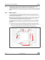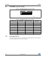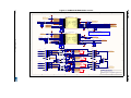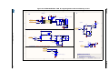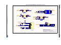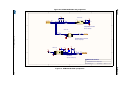
1
UM1807
User manual
STM32303E-EVAL evaluation board
Introduction
The STM32303E-EVAL evaluation board has been designed as a complete demonstration
and development platform for STMicroelectronic's ARM® Cortex®-M4 core-based
STM32F303VET6 microcontrollers. It features two I2Cs, three SPIs, five USARTs, one
CAN, four 12-bit ADCs, two 12-bit DACs, internal 64-KByte Data SRAM, 16-KByte Program
SRAM and 512-KByte Flash, Touch sensing, USB FS, JTAG debugging support. This
evaluation board can be used as the reference design for user application development but
it is not considered as a final application.
The full range of hardware features on the board help you to evaluate all peripherals (USB
FS, USART, Audio DAC and ADC, TFT color LCD, IrDA, LDR, MicroSD card, Motor control
connectors, Humidity Sensor, High Brightness LED, CAN, IR, EEPROM, Touch Sensing
Buttons & Temperature Sensor… etc.) and to develop your own applications. Extension
headers make it possible to easily connect a daughter board or a wrapping board for your
specific application.
An ST-LINK/V2 is integrated on the board as an embedded in-circuit debugger and
programmer for the STM32 MCU.
Figure 1. STM32303E-EVAL evaluation board
October 2014
DocID026738 Rev 1
1/61
www.st.com
1
Contents
UM1807
Contents
1
2
3
Overview . . . . . . . . . . . . . . . . . . . . . . . . . . . . . . . . . . . . . . . . . . . . . . . . . . 6
1.1
Features . . . . . . . . . . . . . . . . . . . . . . . . . . . . . . . . . . . . . . . . . . . . . . . . . . . 6
1.2
Demonstration software . . . . . . . . . . . . . . . . . . . . . . . . . . . . . . . . . . . . . . . 6
1.3
Order code . . . . . . . . . . . . . . . . . . . . . . . . . . . . . . . . . . . . . . . . . . . . . . . . . 6
1.4
Delivery recommendations . . . . . . . . . . . . . . . . . . . . . . . . . . . . . . . . . . . . . 7
Hardware layout and configuration . . . . . . . . . . . . . . . . . . . . . . . . . . . . . 8
2.1
Development and debug support . . . . . . . . . . . . . . . . . . . . . . . . . . . . . . . 10
2.2
Power supply . . . . . . . . . . . . . . . . . . . . . . . . . . . . . . . . . . . . . . . . . . . . . . .11
2.3
Clock source . . . . . . . . . . . . . . . . . . . . . . . . . . . . . . . . . . . . . . . . . . . . . . . 13
2.4
Reset source . . . . . . . . . . . . . . . . . . . . . . . . . . . . . . . . . . . . . . . . . . . . . . 14
2.5
Boot option . . . . . . . . . . . . . . . . . . . . . . . . . . . . . . . . . . . . . . . . . . . . . . . . 14
2.6
Audio . . . . . . . . . . . . . . . . . . . . . . . . . . . . . . . . . . . . . . . . . . . . . . . . . . . . 15
2.7
USB . . . . . . . . . . . . . . . . . . . . . . . . . . . . . . . . . . . . . . . . . . . . . . . . . . . . . 16
2.8
RS232, RS-485 and IrDA . . . . . . . . . . . . . . . . . . . . . . . . . . . . . . . . . . . . . 16
2.9
Touch-sensing buttons . . . . . . . . . . . . . . . . . . . . . . . . . . . . . . . . . . . . . . . 17
2.10
MicroSD card . . . . . . . . . . . . . . . . . . . . . . . . . . . . . . . . . . . . . . . . . . . . . . 18
2.11
Serial EEPROM . . . . . . . . . . . . . . . . . . . . . . . . . . . . . . . . . . . . . . . . . . . . 18
2.12
RF EEPROM . . . . . . . . . . . . . . . . . . . . . . . . . . . . . . . . . . . . . . . . . . . . . . 18
2.13
EEPROM . . . . . . . . . . . . . . . . . . . . . . . . . . . . . . . . . . . . . . . . . . . . . . . . . 19
2.14
CAN . . . . . . . . . . . . . . . . . . . . . . . . . . . . . . . . . . . . . . . . . . . . . . . . . . . . . 19
2.15
IR LED and IR receiver . . . . . . . . . . . . . . . . . . . . . . . . . . . . . . . . . . . . . . 19
2.16
High brightness LED . . . . . . . . . . . . . . . . . . . . . . . . . . . . . . . . . . . . . . . . 19
2.17
Humidity sensor . . . . . . . . . . . . . . . . . . . . . . . . . . . . . . . . . . . . . . . . . . . . 20
2.18
Comparator . . . . . . . . . . . . . . . . . . . . . . . . . . . . . . . . . . . . . . . . . . . . . . . 20
2.19
Temperature sensor . . . . . . . . . . . . . . . . . . . . . . . . . . . . . . . . . . . . . . . . . 20
2.20
Display and input devices . . . . . . . . . . . . . . . . . . . . . . . . . . . . . . . . . . . . . 21
2.21
Motor control . . . . . . . . . . . . . . . . . . . . . . . . . . . . . . . . . . . . . . . . . . . . . . 22
Connectors . . . . . . . . . . . . . . . . . . . . . . . . . . . . . . . . . . . . . . . . . . . . . . . 27
3.1
2/61
RF EEPROM daughter board connector (CN1) . . . . . . . . . . . . . . . . . . . . 27
DocID026738 Rev 1
UM1807
4
Contents
3.2
Motor control connector (CN2) . . . . . . . . . . . . . . . . . . . . . . . . . . . . . . . . . 28
3.3
CAN D-type 9-pin male connector (CN3) . . . . . . . . . . . . . . . . . . . . . . . . . 29
3.4
Motor control connector (CN4) . . . . . . . . . . . . . . . . . . . . . . . . . . . . . . . . . 30
3.5
ST-LINK/V2 USB type-B connector (CN5) . . . . . . . . . . . . . . . . . . . . . . . . 31
3.6
Daughter board extension connectors (CN6 and CN7) . . . . . . . . . . . . . . 32
3.7
RS232 and RS485 connector (CN8) . . . . . . . . . . . . . . . . . . . . . . . . . . . . 36
3.8
ETM Trace debugging connector (CN9) . . . . . . . . . . . . . . . . . . . . . . . . . 37
3.9
JTAG/SWD connector (CN10) . . . . . . . . . . . . . . . . . . . . . . . . . . . . . . . . . 38
3.10
Audio jack (CN11) . . . . . . . . . . . . . . . . . . . . . . . . . . . . . . . . . . . . . . . . . . 38
3.11
User USB type-B connector (CN12) . . . . . . . . . . . . . . . . . . . . . . . . . . . . . 39
3.12
ST-LINK/V2 programming connector (CN13) . . . . . . . . . . . . . . . . . . . . . . 39
3.13
Power connector (CN14) . . . . . . . . . . . . . . . . . . . . . . . . . . . . . . . . . . . . . 39
3.14
TFT LCD connector (CN15) . . . . . . . . . . . . . . . . . . . . . . . . . . . . . . . . . . . 40
3.15
MicroSD connector (CN16) . . . . . . . . . . . . . . . . . . . . . . . . . . . . . . . . . . . 40
Schematics . . . . . . . . . . . . . . . . . . . . . . . . . . . . . . . . . . . . . . . . . . . . . . . 41
Appendix A STM32303E-EVAL I/O assignment . . . . . . . . . . . . . . . . . . . . . . . . . . 55
Appendix B Mechanical dimensions. . . . . . . . . . . . . . . . . . . . . . . . . . . . . . . . . . . 59
5
Revision history . . . . . . . . . . . . . . . . . . . . . . . . . . . . . . . . . . . . . . . . . . . 60
DocID026738 Rev 1
3/61
3
List of tables
UM1807
List of tables
Table 1.
Table 2.
Table 3.
Table 4.
Table 5.
Table 6.
Table 7.
Table 8.
Table 9.
Table 10.
Table 11.
Table 12.
Table 13.
Table 14.
Table 15.
Table 16.
Table 17.
Table 18.
Table 19.
Table 20.
Table 21.
Table 22.
Table 23.
Table 24.
Table 25.
Table 26.
Table 27.
Table 28.
Table 29.
Table 30.
Table 31.
Table 32.
Table 33.
Table 34.
Table 35.
4/61
Third-party support of ST-LINK/V2 . . . . . . . . . . . . . . . . . . . . . . . . . . . . . . . . . . . . . . . . . . . 10
Power supply jumper settings . . . . . . . . . . . . . . . . . . . . . . . . . . . . . . . . . . . . . . . . . . . . . . . 11
Power mode related jumpers . . . . . . . . . . . . . . . . . . . . . . . . . . . . . . . . . . . . . . . . . . . . . . . 12
Low voltage limitation . . . . . . . . . . . . . . . . . . . . . . . . . . . . . . . . . . . . . . . . . . . . . . . . . . . . . 13
32 kHz crystal X1 related solder bridges . . . . . . . . . . . . . . . . . . . . . . . . . . . . . . . . . . . . . . 13
8 MHz crystal X2 related solder bridges . . . . . . . . . . . . . . . . . . . . . . . . . . . . . . . . . . . . . . . 14
Boot-related switch . . . . . . . . . . . . . . . . . . . . . . . . . . . . . . . . . . . . . . . . . . . . . . . . . . . . . . . 15
Boot0-related jumper . . . . . . . . . . . . . . . . . . . . . . . . . . . . . . . . . . . . . . . . . . . . . . . . . . . . . 15
Audio-related jumpers. . . . . . . . . . . . . . . . . . . . . . . . . . . . . . . . . . . . . . . . . . . . . . . . . . . . . 15
RS232, RS485 and IrDA related jumpers . . . . . . . . . . . . . . . . . . . . . . . . . . . . . . . . . . . . . . 17
RS485 related solder bridges . . . . . . . . . . . . . . . . . . . . . . . . . . . . . . . . . . . . . . . . . . . . . . . 17
Touch-sensing button related solder bridges . . . . . . . . . . . . . . . . . . . . . . . . . . . . . . . . . . . 17
EEPROM Related Jumpers . . . . . . . . . . . . . . . . . . . . . . . . . . . . . . . . . . . . . . . . . . . . . . . . 19
CAN related jumpers . . . . . . . . . . . . . . . . . . . . . . . . . . . . . . . . . . . . . . . . . . . . . . . . . . . . . 19
Humidity sensor related jumper . . . . . . . . . . . . . . . . . . . . . . . . . . . . . . . . . . . . . . . . . . . . . 20
Temperature sensor related jumpers . . . . . . . . . . . . . . . . . . . . . . . . . . . . . . . . . . . . . . . . . 21
LCD modules . . . . . . . . . . . . . . . . . . . . . . . . . . . . . . . . . . . . . . . . . . . . . . . . . . . . . . . . . . . 21
Motor control related jumpers . . . . . . . . . . . . . . . . . . . . . . . . . . . . . . . . . . . . . . . . . . . . . . . 23
Motor control related switches and solder bridges in OAM position . . . . . . . . . . . . . . . . . . 24
Motor control related switches and solder bridges in PGM position . . . . . . . . . . . . . . . . . . 25
RF EEPROM daughter board connector (CN1) . . . . . . . . . . . . . . . . . . . . . . . . . . . . . . . . . 27
Motor control 1 connector (CN2) . . . . . . . . . . . . . . . . . . . . . . . . . . . . . . . . . . . . . . . . . . . . 28
CAN D-type 9-pin male connector (CN3) . . . . . . . . . . . . . . . . . . . . . . . . . . . . . . . . . . . . . . 29
Motor control 2 connector (CN4) . . . . . . . . . . . . . . . . . . . . . . . . . . . . . . . . . . . . . . . . . . . . 30
USB type-B connector (CN5) . . . . . . . . . . . . . . . . . . . . . . . . . . . . . . . . . . . . . . . . . . . . . . . 31
Daughter board extension connector (CN6) . . . . . . . . . . . . . . . . . . . . . . . . . . . . . . . . . . . . 32
Daughter board extension connector (CN7) . . . . . . . . . . . . . . . . . . . . . . . . . . . . . . . . . . . . 34
RS232 and RS485 connector (CN8) with ISP support . . . . . . . . . . . . . . . . . . . . . . . . . . . . 36
ETM trace debugging connector (CN9) . . . . . . . . . . . . . . . . . . . . . . . . . . . . . . . . . . . . . . . 37
JTAG/SWD debugging connector CN10 . . . . . . . . . . . . . . . . . . . . . . . . . . . . . . . . . . . . . . 38
USB type-B connector (CN12) . . . . . . . . . . . . . . . . . . . . . . . . . . . . . . . . . . . . . . . . . . . . . . 39
MicroSD connector (CN16). . . . . . . . . . . . . . . . . . . . . . . . . . . . . . . . . . . . . . . . . . . . . . . . . 40
STM32303E-EVAL I/O assignment . . . . . . . . . . . . . . . . . . . . . . . . . . . . . . . . . . . . . . . . . . 55
Mechanical dimensions . . . . . . . . . . . . . . . . . . . . . . . . . . . . . . . . . . . . . . . . . . . . . . . . . . . 59
Document revision history . . . . . . . . . . . . . . . . . . . . . . . . . . . . . . . . . . . . . . . . . . . . . . . . . 60
DocID026738 Rev 1
UM1807
List of figures
List of figures
Figure 1.
Figure 2.
Figure 3.
Figure 4.
Figure 5.
Figure 6.
Figure 7.
Figure 8.
Figure 9.
Figure 10.
Figure 11.
Figure 12.
Figure 13.
Figure 14.
Figure 15.
Figure 16.
Figure 17.
Figure 18.
Figure 19.
Figure 20.
Figure 21.
Figure 22.
Figure 23.
Figure 24.
Figure 25.
Figure 26.
Figure 27.
Figure 28.
Figure 29.
Figure 30.
Figure 31.
Figure 32.
STM32303E-EVAL evaluation board . . . . . . . . . . . . . . . . . . . . . . . . . . . . . . . . . . . . . . . . . . 1
Hardware block diagram . . . . . . . . . . . . . . . . . . . . . . . . . . . . . . . . . . . . . . . . . . . . . . . . . . . . 8
STM32303E-EVAL evaluation board layout . . . . . . . . . . . . . . . . . . . . . . . . . . . . . . . . . . . . . 9
STM32303E-EVAL comparator features . . . . . . . . . . . . . . . . . . . . . . . . . . . . . . . . . . . . . . 20
Resistor positions on the PCB board: even number removing . . . . . . . . . . . . . . . . . . . . . . 22
Resistor positions on the PCB board: odd number mounting . . . . . . . . . . . . . . . . . . . . . . . 23
RF EEPROM daughter board connector (CN1) . . . . . . . . . . . . . . . . . . . . . . . . . . . . . . . . . 27
Motor control 1 connector (CN2) . . . . . . . . . . . . . . . . . . . . . . . . . . . . . . . . . . . . . . . . . . . . 28
CAN D-type 9-pin male connector (CN3) . . . . . . . . . . . . . . . . . . . . . . . . . . . . . . . . . . . . . . 29
Motor control 2 connector (CN4) . . . . . . . . . . . . . . . . . . . . . . . . . . . . . . . . . . . . . . . . . . . . 30
USB type-B connector (CN5) . . . . . . . . . . . . . . . . . . . . . . . . . . . . . . . . . . . . . . . . . . . . . . . 31
RS232 and RS485 connector . . . . . . . . . . . . . . . . . . . . . . . . . . . . . . . . . . . . . . . . . . . . . . . 36
ETM Trace debugging connector (CN9) . . . . . . . . . . . . . . . . . . . . . . . . . . . . . . . . . . . . . . . 37
JTAG/SWD debugging connector (CN10) . . . . . . . . . . . . . . . . . . . . . . . . . . . . . . . . . . . . . 38
USB type-B connector (CN12) . . . . . . . . . . . . . . . . . . . . . . . . . . . . . . . . . . . . . . . . . . . . . . 39
Power supply connector (CN14) . . . . . . . . . . . . . . . . . . . . . . . . . . . . . . . . . . . . . . . . . . . . . 39
MicroSD connector (CN16). . . . . . . . . . . . . . . . . . . . . . . . . . . . . . . . . . . . . . . . . . . . . . . . . 40
STM32303E-EVAL board (MB1019) . . . . . . . . . . . . . . . . . . . . . . . . . . . . . . . . . . . . . . . . . 41
STM32303E-EVAL MCU . . . . . . . . . . . . . . . . . . . . . . . . . . . . . . . . . . . . . . . . . . . . . . . . . . 42
STM32303E-EVAL Power . . . . . . . . . . . . . . . . . . . . . . . . . . . . . . . . . . . . . . . . . . . . . . . . . 43
STM32303E-EVAL RS232, RS485 and IrDA . . . . . . . . . . . . . . . . . . . . . . . . . . . . . . . . . . . 44
STM32303E-EVAL Audio . . . . . . . . . . . . . . . . . . . . . . . . . . . . . . . . . . . . . . . . . . . . . . . . . 45
STM32303E-EVAL Motor control . . . . . . . . . . . . . . . . . . . . . . . . . . . . . . . . . . . . . . . . . . . . 46
STM32303E-EVAL CAN, IR, High-brightness LED and Humidity sensor . . . . . . . . . . . . . 47
STM32303E-EVAL LCD, SDCard and Flash . . . . . . . . . . . . . . . . . . . . . . . . . . . . . . . . . . . 48
STM32303E-EVAL I2C peripherals . . . . . . . . . . . . . . . . . . . . . . . . . . . . . . . . . . . . . . . . . . 49
STM32303E-EVAL peripherals . . . . . . . . . . . . . . . . . . . . . . . . . . . . . . . . . . . . . . . . . . . . . 49
STM32303E-EVAL ST-LINK (JTAG only) . . . . . . . . . . . . . . . . . . . . . . . . . . . . . . . . . . . . . 51
STM32303E-EVAL JTAG and Trace . . . . . . . . . . . . . . . . . . . . . . . . . . . . . . . . . . . . . . . . . 52
TM32330C-EVAL touch sensing . . . . . . . . . . . . . . . . . . . . . . . . . . . . . . . . . . . . . . . . . . . . 53
Color LCD daughter board (MB895) . . . . . . . . . . . . . . . . . . . . . . . . . . . . . . . . . . . . . . . . . . 54
Mechanical dimensions . . . . . . . . . . . . . . . . . . . . . . . . . . . . . . . . . . . . . . . . . . . . . . . . . . . 59
DocID026738 Rev 1
5/61
5
Overview
UM1807
1
Overview
1.1
Features
1.2
•
Four 5 V power supply options: Power jack, ST-LINK/V2 USB connector, User USB
connector or daughter board
•
I2S Audio DAC, stereo audio jack which supports headset with microphone
•
2-Gbyte or more SPI interface microSD card
•
I2C compatible serial interface temperature sensor, EEPROM and RF EEPROM
•
RS232 and RS485 communication
•
IrDA transceiver
•
JTAG/SWD and ETM trace debug support, ST-LINK/V2 embedded
•
1-Mbit SPI serial Flash memory
•
240x320 TFT color LCD connected to the SPI interface
•
Joystick with 4-direction control and selector
•
Reset, Tamper or Key button
•
4-color user LEDs and high brightness LED
•
Humidity sensor
•
Extension connectors for daughter board or wrapping board
•
MCU voltage choice: 3.3 V or adjustable from 2.0 V to 3.6 V
•
USB FS connector
•
Touch-sensing buttons
•
RTC with backup battery
•
CAN2.0A/B compliant connection
•
Light-dependent resistor (LDR)
•
IR LED and receiver
•
Potentiometer
•
2 motor control connectors
Demonstration software
The demonstration software is preloaded in the board's Flash memory for an easy
demonstration of the device peripherals in standalone mode. For more information and to
download the latest version available, please refer to the STM32303E-EVAL demonstration
software available on www.st.com.
1.3
Order code
To order the STM32F303VET6 evaluation board, use the STM32303E-EVAL order code.
6/61
DocID026738 Rev 1
UM1807
1.4
Overview
Delivery recommendations
Before using the board for the first time, please verify that nothing was damaged during
shipment and that no components are unplugged or lost.
When the board is extracted from its plastic bag, please check that no component remains
in the bag.
The main components to verify are:
1.
The 8 MHz crystal (X2) which may have been removed from its socket by a shock.
2.
The MicroSD card which may have been ejected from the CN16 connector (right side
of the board).
3.
The dual-interface EEPROM board (ANT7-M24LR-A) which may have been unplugged
from the CN1 connector (top left corner of the board).
For all information concerning the version of the MCU used on the board, its specification
and possible related limitations, please visit the ST web site to download the relevant data
sheet and erratasheet.
Warning:
This equipment contains parts (principally an LCD), subject to
be damaged by electrostatic discharge (ESD). Before touching
the LCD or its connector (CN1 on MB895), use one of these
following ESD precautionary procedures:
Wear a ground strap. The function of such strap is to rapidly
and safely dissipate personnel static charge to the ground.
Touch the ground before all other nets or components on
board. The easiest way to proceed is to touch with a finger the
shield available on DB9 connectors (CN3 & CN8), USB
connector (CN5) or uSD card connector (CN16).
DocID026738 Rev 1
7/61
60
Hardware layout and configuration
2
UM1807
Hardware layout and configuration
The STM32303E-EVAL evaluation board has been designed around the STM32F303VET6
microcontroller (100-pin TQFP package). The hardware block diagram in Figure 2 illustrates
the connection between the STM32F303VET6 microcontroller and its peripherals (color
LCD, touch sensing buttons, USB FS connector, motor control connectors, temperature
sensor, USART, IrDA, Audio, EEPROM,RF EEPROM, MicroSD card and embedded
ST-LINK). Figure 3 helps to locate these features on the actual evaluation board.
Figure 2. Hardware block diagram
DŽƚŽƌŽŶƚƌŽů
ĐŽŶŶĞĐƚŽƌϭ
DŽƚŽƌŽŶƚƌŽů
ĐŽŶŶĞĐƚŽƌϮ
Z^ϮϯϮ
ƚƌĂŶƐĐĞŝǀĞƌ
:ŽLJƐƚŝĐŬ
>Ɛ
'W/K
h^Zdϭ
sŽůƚĂŐĞ
ƚƌĂŶƐůĂƚŽƌ
Z^ϰϴϱ
ƚƌĂŶƐĐĞŝǀĞƌ
<ĞLJ
ďƵƚƚŽŶ
WŚŽƚŽͲZ
/ƌ
ƚƌĂŶƐĐĞŝǀĞƌ
ŽŵƉĂƌĂƚŽƌ
dŽƵĐŚ^ĞŶƐŝŶŐ
ƵƚƚŽŶƐ
d^
ĐŽŶƚƌŽůůĞƌ
,ŝŐŚĐƵƌƌĞŶƚ
>Ɛ
ŽŵƉĂƌĂƚŽƌ
WtD
,ƵŵŝĚŝƚLJ
^ĞŶƐŽƌ
ŵďĞĚĚĞĚ
^d Ͳ>/E<ͬsϮ
h^dLJƉĞ
ĐŽŶŶĞĐƚŽƌ
:d'
:d'ΘdƌĂĐĞ
ĐŽŶŶĞĐƚŽƌ
DŝĐƌŽ^
ĐĂƌĚ
^dDϯϮ&ϯϬϯsdϲ
^W/Ϯ
d/D
sŽůƚĂŐĞ
ƚƌĂŶƐůĂƚŽƌ
7)7FRORU
/&'
WZKD
WtD
h^
ĐŽŶŶĞĐƚŽƌ
Z^ϮϯϮͬZ^ϰϴϱ
ĐŽŶŶĞĐƚŽƌ
h^&^
/Ϯ^
ƵĚŝŽ
ŽĚĞĐΘ
ŵƉůŝĨŝĞƌ
,ĞĂĚƐĞƚ:ĂĐŬ
DŝĐƌŽƉŚŽŶĞ
EĚƌŝǀĞƌ
ΘŽŶŶĞĐƚŽƌ
E
/Z>Θ
/ZƌĞĐĞŝǀĞƌ
/Zd/D
WtD
WŽƚĞŶƚŝŽŵĞƚĞƌ
ŽŵƉĂƌĂƚŽƌ
WZKD
/Ϯ
Z&WZKD
ĐŽŶŶĞĐƚŽƌ
dĞŵƉĞƌĂƚƵƌĞ
^ĞŶƐŽƌ
Ϯ͘ϬsƚŽϯ͘ϲs
ĂĚũƵƐƚĂďůĞ
ƌĞŐƵůĂƚŽƌ
ϯ͘ϯs
ƌĞŐƵůĂƚŽƌ
džƚĞŶƐŝŽŶ
ĐŽŶŶĞĐƚŽƌĨŽƌ
'W/KƐ
069
Note:
8/61
‘o’ = I/O shared with Motor Control.
DocID026738 Rev 1
UM1807
Hardware layout and configuration
Figure 3. STM32303E-EVAL evaluation board layout
DocID026738 Rev 1
9/61
60
Hardware layout and configuration
2.1
UM1807
Development and debug support
Version 2 of ST-LINK, called ST-LINK/V2, is embedded on the board. This tool allows
program loading and debugging of the STM32 on board using a JTAG or SWD interface.
The third-party debug tools are also supported by the JTAG/SWD connector, CN10, or the
ETM Trace connector, CN9.
A specific driver needs to be installed on your PC for communication with embedded STLINK/V2.The install shield called ST-LINK_V2_USBdriver.exe is available at
www.st.com/stlinkv2.
Third-party toolchains, Atollic TrueSTUDIO, KEIL® MDK-ARM, IAR® EWARM and Tasking
VX-Toolset support ST-LINK/V2 according to Table 1.
Table 1. Third-party support of ST-LINK/V2
Third party
Toolchain
Version
Atollic
TrueSTUDIO
2.1
IAR®
EWARM
6.20
Keil®
MDK-ARM
TASKING
4.20
®
VX-toolset for ARM
Cortex®-M
4.0.1
The embedded ST-LINK/V2 is connected to the PC via a standard USB cable connected to
connector CN5.The bicolor LED LD8 (COM) advises on the status of the communication as
follows:
Note:
•
Slow blinking red/off: at power on before USB init
•
Fast blinking red/off: after the first correct communication between PC and ST-Link/V2
(enumeration)
•
Red LED on: when the initialization between PC and ST-LINK/V2 has been successful
•
Green LED on: after a successful target communication initialization
•
Blinking red/green: during communication with target
•
Red on: communication finished and OK
•
Orange on: communication failure
The board can be powered via CN5 (Embedded ST/LINK/V2 USB connector) even if an
external tool is connected to CN9 (ETM Trace connector) or CN10 (External JTAG & SWD
connector).
R111 needs to be removed when using ETM 4-bit function. In this case, the key button does
not work.
10/61
DocID026738 Rev 1
UM1807
2.2
Hardware layout and configuration
Power supply
The STM32303E-EVAL evaluation board has been designed to be powered by 5 V DC
power supply and to be protected by PolyZen from wrong power plug-in event. The
evaluation board can be configured to use any of the four following sources of power supply:
•
5 V DC power adapter connected to CN14, the power jack on the board (Power supply
unit (PSU) on silkscreen of JP14). The external power supply is not provided with the
board.
•
5 V DC power with 500 mA limitation from CN5, the USB type B connector of STLINK/V2 (USB 5 V power source on silkscreen of JP14 ( STlk)).
•
5V DC power with 500mA limitation from CN12, the USB type B connector (USB 5V
power source on silkscreen of JP14 (USB)).
•
5V DC power from CN6 & CN7, the extension connectors for daughter board (daughter
board power source on silkscreen of JP14 (D5V)).
The power s4upply is configured by setting the related jumpers JP14, JP15, JP16 and JP17
as described in Table 2.
Table 2. Power supply jumper settings
Setting
Description
STlk
PSU
U5V
D5V
Jumper
JP14 is used to select one of the four possible power supply resources.
For power supply from the daughter board connectors (CN6 and CN7) to
STM32303E-EVAL only, JP14 is set as shown to the right:
For power supply from USB (CN12) to STM32303E-EVAL only, JP14 is set as
shown to the right:
JP14
For power supply jack (CN14) to the STM32303E-EVAL only, JP14 is set as
shown to the right:
For power supply from USB connector of ST-LINK/V2 (CN5) to STM32303E EVAL only, JP14 is set as shown to the right (default setting):
For power supply from power supply jack (CN14) to both STM32303E -EVAL and
daughter board connected on CN6 and CN7, JP14 is set as shown to the right
(the daughter board must not have its own power supply connected):
Vbat is connected to the battery when JP16 is set as shown to the right:
JP16
Vbat is connected to VDD power when JP16 is set as shown to the right (default
setting):
DocID026738 Rev 1
11/61
60
Hardware layout and configuration
UM1807
Table 2. Power supply jumper settings (continued)
Setting
Description
STlk
PSU
U5V
D5V
Jumper
VDD is connected to fixed +3.3 V DC power when JP15 is set as shown to the
right (default setting):
JP15
VDD is connected to adjustable DC power from 2.0 V to 3.6 V when JP15 is set
as shown to the right:
VDDA power is connected to VDD when JP17 is set as shown to the right (default
setting):
JP17
VDDA power is connected to fixed +3.3 V DC power when JP17 is set as shown
to the right:
Note:
Though technically adjustable from 2.0 V to 3.6 V, VDD has been designed to adjust from
2.1 V to 3.5 V considering some peripheral component specifications.
LED LD8 is lit when the STM32303E-EVAL evaluation board is correctly powered by 5 V.
A total of three power modes are supported on the board, and can be configured by setting
the related jumpers JP15 and JP17 as described in Table 3 and the Note below.
•
Mode1: VDD and VDDA were connected together and powered by fixed 3.3 V.
•
Mode2: VDD and VDDA were connected together and powered by an adjustable
voltage from 2.0 V to 3.6 V.
•
Mode3: VDD is powered by an adjustable voltage from 2.0 V to 3.6 V while VDDA is
powered by fixed 3.3 V.
Table 3. Power mode related jumpers
Power mode configuration
Power mode
JP15
JP17
MCU IDD
measurement
OK
Mode1
Not allowed
12/61
DocID026738 Rev 1
UM1807
Hardware layout and configuration
Table 3. Power mode related jumpers (continued)
Power mode configuration
MCU IDD
measurement
Power mode
JP15
Note:
JP17
Mode2
OK
Mode3
Not allowed
MCU IDD measurement can be done by the current meter which is mounted on JP12 when it
is open.
JP11 must be open (disconnect VDDA from all analog power VDD_ANA connected to the
analog circuit) for MCU IDD measurement.
Due to the characters of some peripheral components' specification, the low voltage
limitations related to the operating voltage of the peripherals (a component will not work
correctly when the power level is under the low voltage limitation) are shown in Table 4.
Table 4. Low voltage limitation
Peripheral
Component
I/O name
Low voltage limitation
USB
CN12
USB
3V
CAN
CN3
CAN
3V
Temperature sensor
U1
I2C2
2.25V
Note:
When an external DC 5V power supply is used to power the STM32303E-EVAL, it needs to
be connected to CN14 after verifying the correct polarity as explained in Section 3.13.
Caution:
RISK OF EXPLOSION IF THE BATTERY IS REPLACED BY AN INCORRECT TYPE.
DISPOSE OF USED BATTERIES ACCORDING TO THE INSTRUCTIONS.
2.3
Clock source
Two clock sources are available on the STM32303E-EVAL evaluation board for
STM32F303VET6 and RTC embedded:
•
X1, 32 kHz crystal for embedded RTC
•
X2, 8 MHz crystal with socket for the STM32F303VET6 microcontroller; it can be
removed from the socket when an internal RC clock is used.
Table 5. 32 kHz crystal X1 related solder bridges
Solder bridge
Description
PC14 is connected to the 32 KHz crystal when SB12 is open (default setting).
SB12
PC14 is connected to the extension connector CN6 when SB12 is closed. In such
a case, R196 must be removed to avoid disturbance due to the 32 KHz quartz.
DocID026738 Rev 1
13/61
60
Hardware layout and configuration
UM1807
Table 5. 32 kHz crystal X1 related solder bridges (continued)
Solder bridge
Description
PC15 is connected to the 32 KHz crystal when SB13 is open (default setting).
SB13
PC15 is connected to the extension connector CN6 when SB13 is closed. In such
a case, R197 must be removed to avoid disturbance due to the 32 KHz quartz.
Table 6. 8 MHz crystal X2 related solder bridges
Solder bridge
Description
PF0 is connected to the 8 MHz crystal when SB14 is open (default setting).
SB14
PF0 is connected to the extension connector CN7 when SB14 is closed. In such a
case, C51 and X2 must be removed to avoid disturbance due to the 8 MHz
quartz.
PF1 is connected to the 8 MHz crystal when SB15 is open (default setting).
SB15
2.4
PF1 is connected to the extension connector CN7 when SB15 is closed. In such a
case, R205 must be removed.
Reset source
The reset signal of the STM32303E-EVAL evaluation board is low active and the reset
sources include:
•
Reset button (B1)
•
Debugging tools from JTAG/SWD connector (CN10) and ETM trace connector (CN9)
•
Daughter board from CN7
•
Embedded ST-LINK/V2
•
RS232 connector (CN8) for ISP
Note:
The JP10 jumper must be closed for RESET handled by pin8 of RS232 connector, CN8
(CTS signal).
2.5
Boot option
The STM32303E-EVAL evaluation board can boot from:
•
the embedded user Flash
•
the system memory with boot loader for ISP
•
the embedded SRAM for debugging
The boot option is configured by setting switch SW1 (BOOT0) and bit 12 of USER OPTION
BYTES (BOOT1) in Small Information block (SIF). BOOT0 can also be configured via the
RS232 connector, CN8.
14/61
DocID026738 Rev 1
UM1807
Hardware layout and configuration
Table 7. Boot-related switch
Switch
configuration
bit 12 of USER OPTION
BYTES
0 <----> 1
SW1
0 <----> 1
SW1
0 <----> 1
SW1
STM32303E-EVAL boot
X
From the user Flash when SW1 is set as
shown to the left (default setting)
0
From the embedded SRAM when SW1 and
bit12 in USER OPTION BYTES are set as
shown to the left.
1
From the system memory when SW1 and
bit12 in USER OPTION BYTES are set as
shown to the left.
Table 8. Boot0-related jumper
Jumper
JP9
2.6
Description
Bootloader_BOOT0 is managed by pin 6 of connector CN8 (RS232 DSR
signal) when JP9 is closed. This configuration is only used for the boot
loader application.
Default Setting: Not fitted
Audio
The STM32303E-EVAL evaluation board supports stereo audio play and microphone
recording by an external headset connected on audio jack CN11. An audio DAC CS42L52 is
connected to the I2S port of the STM32F303VET6 microcontroller. The microphone on
headset or microphone which is reserved on board (U26, default unmounted) are connected
to ADC of CS42L52. The CS42L52 can be configured via I2C2 and be driven by either
I2S_MCK at PA9 or the external I2S clock mode supported by an external PLL (U12).
Note:
Please keep VDD to 3.3 V (Power mode 1 in Section 2.2) when using external PLL CS2200.
The I2C communication depends on JP5 and JP6 jumper setting.
Table 9. Audio-related jumpers
Jumper
Description
JP5
PA10 is used as I2C standard mode and it is connected to
I2C2_SDA signal on Audio DAC, Audio external PLL,
temperature sensor and RF EEPROM connector when JP5 is
set as shown to the right (default setting):
Setting
PA10 is used as I2C fast mode and it is connected to
I2C2_SDA_F signal on EEPROM when JP5 is set as shown to
the right:
DocID026738 Rev 1
15/61
60
Hardware layout and configuration
UM1807
Table 9. Audio-related jumpers (continued)
Jumper
Description
JP6
PF6 is used as I2C standard mode and it is connected to
I2C2_SCL signal on Audio DAC, Audio external PLL,
temperature sensor and RF EEPROM connector when JP6 is
set as shown to the right (default setting):
Setting
PF6 is used as I2C fast mode and it is connected to
I2C2_SCL_F signal on EEPROM when JP6 is set as shown to
the right:
PA9 is connected to I2S_MCK signal on CS42L52 when JP18
is set as shown to the right (default setting)
JP18
PA9 is connected to IR_IN signal on TSOP34836 when JP18 is
set as shown to the right:
The I2C address of CS42L52 is 0b1001010, and that of External PLL CS2200 is
0b1001110.
2.7
USB
The STM32303E-EVAL evaluation board supports USB2.0 compliant full speed
communication via a USB type B connector (CN12). The evaluation board can be powered
by this USB connection at 5 V DC with 500 mA current.
A USB disconnection simulation can be implemented by controlling the 1.5 K pull-up resistor
on the USB+ line and by detecting the 5 V power on the USB connector (CN12) via a
resistor connected to PB8.
USB will work properly when VDD > 3 V.
2.8
RS232, RS-485 and IrDA
The RS232, RS-485 and IrDA communication is supported by D-type 9-pin RS232/RS-485
connectors (CN8) and IrDA transceiver (U10) which is connected to USART1 of
STM32F303VET6 on the STM32303E-EVAL evaluation board. Bootloader_RESET &
Bootloader_BOOT0 signals are added on the RS232 connector (CN8) for ISP support.
16/61
DocID026738 Rev 1
UM1807
Hardware layout and configuration
Table 10. RS232, RS485 and IrDA related jumpers
Setting
Description
RS232_RX
RS485_RX
IRDA_RX
Jumper
RS232_RX is connected to the RS232 transceiver
and the RS232 communication is enabled when JP13
is set as shown to the right (default setting):
RS485_RX is connected to the RS485 transceiver
and the RS485 communication is enabled when JP13
is set as shown to the right:
JP13
IrDA_RX is connected to the IrDA transceiver and the
IrDA communication is enabled when JP13 is set as
shown to the right:
The RS485 communication is supported by the RS485 transceiver, ST3485EBDR, which is
connected to pin4 and pin9 of D-type 9-pin connectors CN8 (share the same connector with
USART1).
Table 11. RS485 related solder bridges
Jumper
Description
SB17, SB18
The bus termination is enabled when solder bridge SB16 is closed.
Default setting: Not fitted.
SB16
2.9
The external failsafe biasing is enabled when solder bridges SB17 and
SB18 are closed.
Default setting: Not fitted
Touch-sensing buttons
The STM32303E-EVAL evaluation board supports two touch-sensing buttons based on the
charge transfer technology.
Table 12. Touch-sensing button related solder bridges
Solder bridge
Description
PD13 is connected to the touch button when SB6 is open.
(Default setting)
SB6
PD13 is connected to the extension connector CN7 when SB6 is closed. In
such a case, R104 must be removed to avoid disturbance due to the touch
button.
DocID026738 Rev 1
17/61
60
Hardware layout and configuration
UM1807
Table 12. Touch-sensing button related solder bridges (continued)
Solder bridge
Description
PD15 is connected to the touch button when SB7 is open.
(Default setting)
SB7
PD15 is connected to the extension connector CN7 when SB7 is closed. In
such a case, R102 must be removed to avoid disturbance due to the touch
button.
PD12 is connected to the sampling capacitor when SB8 is open.
(Default setting)
SB8
PD12 is connected to the extension connector CN7 when SB8 is closed. In
such a case, C52 must be removed to avoid disturbance due to the
capacitor.
PB12 is connected to the shield when SB9 is open.
(Default setting)
SB9
PB12 is connected to the extension connector CN6 when SB9 is closed. In
such a case, R103 must be removed to avoid disturbance due to the
shield.
PB11 is connected to the shield charge capacitor when SB11 is open.
(Default setting)
SB11
2.10
PB11 is connected to the extension connector CN6 when SB11 is closed.
In such a case, R137 must be removed to avoid disturbance due to the
capacitor.
MicroSD card
The 2 GB (or more) MicroSD card connected to the SPI2 port (Shared with color LCD and
Serial EEPROM) of STM32F303VET6 is available on the board. The MicroSD card
detection is managed by the standard I/O port, PC6.
2.11
Serial EEPROM
A 1 Mbit (M95M01-R) serial EEPROM connected to the SPI2 port (shared with color LCD
and MicroSD card) of STM32F303VET6, serial Flash Chip select is managed by I/O pin
PD7.
2.12
RF EEPROM
The RF EEPROM daughter board, ANT7-M24LR-A, is mounted on CN1 to
STM32F303VET6 via the I2C2 bus.
The I2C address of RF EEPROM is 0b1010000.
The I2C communication depends on JP5 and JP6 jumper setting, as shown in Table 9.
18/61
DocID026738 Rev 1
UM1807
2.13
Hardware layout and configuration
EEPROM
To fit the fast mode requirements, a 1 Mbit EEPROM, M24M01-HR, is directly connected to
the I2C2 bus of STM32F303VET6 by setting JP5 and JP6 jumpers, as shown in Table 9.
Table 13. EEPROM Related Jumpers
Jumper
JP8
JP5, JP6
2.14
Description
The EEPROM is in Write protection mode when JP8 is closed.
Default setting: Not fitted
See Table 9
CAN
The STM32303E-EVAL evaluation board supports one channel of a CAN2.0A/B compliant
bus communication based on the 3.3V CAN transceiver. The high-speed mode, standby
mode and slope control mode are available and can be selected by setting JP4.
Table 14. CAN related jumpers
Jumper
Description
Setting
The CAN transceiver is working in standby mode when JP4
is set as shown to the right:
JP4
JP3
The CAN transceiver is working in high-speed mode when
JP4 is set as shown to the right: (default setting)
The CAN transceiver is working in slope control mode
when JP4 is open.
-
The CAN terminal resistor is enabled when JP3 is fitted.
Default setting: Not fitted
-
CAN will work properly when VDD > 3 V.
2.15
IR LED and IR receiver
The IR receiver, TSOP34836, is connected to PA9 of STM32F303VET6 and the IR LED is
driven by PB9 through transistors T4 and T5 on the board. The IR receiver depends on
JP18 jumper setting, as shown in Table 9.
Note:
The IR LED may be driven by PB9 directly when SB19 is closed and R281 is removed.
2.16
High brightness LED
An amber high brightness LED and its power control circuits are on the STM32303E-EVAL
board. The brightness can be adjusted by the PWM signal from STM32F303VET6 through
PE13. The current on the LED can be monitored by the STM32F303 thanks to the voltage
measured on PD14, which corresponds to current through R261 (10 ohm).
DocID026738 Rev 1
19/61
60
Hardware layout and configuration
2.17
UM1807
Humidity sensor
A humidity sensor, HS1101LF, is on the STM32303E-EVAL board. The charge control signal
is connected to the timer in STM32F303VET6 through PC8, and the measured result of
HS1101LF is connected with PB0.
Note:
Please keep VDDA =V DDIO during the measurement.
A 180 pF 1% capacitor, C121, is used to calibrate the humidity sensor by setting JP19.
Table 15. Humidity sensor related jumper
Jumper
Description
Setting
A 180 pF 1% capacitor is connected for calibration when
JP19 is set, as shown to the right:
JP19
A humidity sensor is connected to measure the humidity
when JP19 is set, as shown to the right: (default setting)
2.18
Comparator
VDD_ANA is divided by the resistor bridge of LDR VT9ON1 & 8.2K resistor and connected
to PA0 (COM1_IN-/ADC IN1). VDD_ANA is also divided by the RV2 potentiometer and
connected to PC1 (COM7_IN+/ADC12).
Figure 4. STM32303E-EVAL comparator features
9''B$1$
*3&203B,1
$'&
3$
*3&203B,1
3&
*3&203B,1
*3&203
287
/'5
*1'
9''B$1$
$'&
*1'
*3&203B,1
*3&203
287
069
2.19
Temperature sensor
A temperature sensor, STTS751, is connected to the I2C2 bus of STM32F303VET6 by
setting JP5 and JP6 jumpers, as shown in Table 9.
20/61
DocID026738 Rev 1
UM1807
Hardware layout and configuration
Table 16. Temperature sensor related jumpers
Jumper
Description
JP1
An SMB signal connects to the temperature sensor event signal when JP1
is closed.
Default setting: Not fitted
The I2C address of the temperature sensor is 0b1001000.
STTS751 will work properly when VDD > 2.25V.
Note:
The temperature result measured from PT100 would be a little higher than the ambient
temperature due to the power dissipation of components on the board.
2.20
Display and input devices
The 240x320 TFT color LCD connected to the SPI2 port of STM32F303VET6 (shared with
the MicroSDcard and Serial EEPROM) and four general-purpose color LEDs (LD1, LD2,
LD3, LD4) are available as display devices. The 4-direction joystick (U27) with the selection
and key button (B2) are available as input devices.
The LCD can be enabled by the chip select signal PE0; this signal should be set as an
open-drain output pin in STM32F303VET6. All joystick signals should be set as a pull-down
input pin in STM32F303VET6.
Table 17. LCD modules
TFT LCD CN15
Pin on CN15
Description
Pin connection
1
CS
PE0
2
SCL
PF9
3
SDI
PB15
4
RS
-
5
WR
-
6
RD
-
7
SDO
PB14
8
RESET
RESET#
9
VDD
3.3V
10
VCI
3.3V
11
GND
GND
12
GND
GND
13
BL_VDD
5V
14
BL_Control
5V
15
BL_GND
GND
16
BL_GND
GND
DocID026738 Rev 1
21/61
60
Hardware layout and configuration
UM1807
Note:
The bi-directional voltage translator is implemented on the SPI MOSI signal between
STM32F303VET6 and the LCD to support the 3-wire serial interface of the
AM240320LGTNQW-01H LCD panel. The direction of this voltage translator is controlled by
the PE14 I/O (the PB15 I/O is used as a MOSI when PE14 is high, or as a MISO when PE14
is low).
2.21
Motor control
The STM32303E-EVAL evaluation board supports 2 inductor motor controls via 34-pin
connectors CN2 and CN4, which provide all required control and feedback signals to and
from the motor power-driving board.
Available signals on these connectors include emergency stop, motor speed, 3-phase motor
current, bus voltage, heatsink temperature coming from the motor driving board and 6
channels of PWM control signal going to the motor driving circuit.
Some PCB reworks are needed for motor control applications to disconnect peripherals
which share I/Os with motor control connectors and connect these I/Os to motor control
connectors.
To configure the board for motor control application, please follow the procedure below:
1.
Remove even number resistors from R1 to R58 (R2, R4, R6….R56, R58 except R12
and R22). The resistor positions on the PCB board are shown in Figure 5:
Figure 5. Resistor positions on the PCB board: even number removing
R50
R38
R52
R36
R58
R16
R18
R2
22/61
DocID026738 Rev 1
R14
UM1807
Hardware layout and configuration
2.
Mount odd number resistors from R1 to R57 (R1, R3….R55, R57) except R11 which is
mounted by default with a 0-ohm resistor. The resistor positions on the PCB board are
shown in Figure 6:
Figure 6. Resistor positions on the PCB board: odd number mounting
R49
R51
R37
R35
R57
R1
R15
R13
R17
Table 18. Motor control related jumpers
Jumper
Description
JP2
JP2 should be kept open when the encoder signal is from pin31 of the
motor control connector CN2; it should be kept closed when the analog
signal is from pin31 of CN2 for a special motor.
Default setting: Not fitted
JP7
JP7 should be kept open when the encoder signal is from pin31 of the
motor control connector CN4; it should be kept closed when the analog
signal is from pin31 of CN4 for a special motor.
Default setting: Not fitted
DocID026738 Rev 1
23/61
60
Hardware layout and configuration
UM1807
Table 19. Motor control related switches and solder bridges in OAM position
OAM position
OAM1
Other conditions
Description
R113, R116 mounted
SB2 open
MC1_CurrentA+ connect to OPAMP1_IN+(PA1)
MC1_CurrentB+ connect to OPAMP2_IN1+(PA7)
R113, R116 unmounted
SB2 closed
MC1_CurrentB+ connect to OPAMP1_IN+(PA1)
3SA position
MC1_CurrentC+ connect to OPAMP2_IN2+(PD14)
3SA position
MC1_CurrentC+ connect to OPAMP4_IN1+(PB11)
OAM1
-
R132, R134 mounted
SB5 open
OAM2
MC1_CurrentA+ connect to ADC12(PC2)
MC1_CurrentB+ connect to ADC12(PC3)
MC1_CurrentC+ connect to ADC12(PC0)
MC2_CurrentA+ connect to OPAMP3_IN+(PB0)
MC2_CurrentB+ connect to OPAMP4_IN2 +(PB13)
R132, R134 unmounted
MC2_CurrentB+ connect to OPAMP3_IN+(PB0)
SB5 closed
3SA position
MC2_CurrentC+ connect to OPAMP4_IN1+(PB11)
3SA position
MC2_CurrentC+ connect to OPAMP2_IN2+(PD14)
OAM2
-
24/61
MC2_CurrentA+ connect to ADC34(PD11)
MC2_CurrentB+ connect to ADC34(PD12)
MC2_CurrentC+ connect to ADC34(PD10)
DocID026738 Rev 1
UM1807
Hardware layout and configuration
Table 20. Motor control related switches and solder bridges in PGM position
PGM position
Other conditions
Description
PGM1
-
OPAMP1_IN+,OPAMP2_IN1+, OPAMP2_IN2+
pull-up source connect to +3.3V power
PG3SA position
OPAMP1_IN+, OPAMP2_IN1+, OPAMP2_IN2+
pull-up source connect to DAC_OUT1(PA4)
PGM1
PG3SA position
OPAMP1_IN+, OPAMP2_IN1+ pull-up source
connect to DAC_OUT1(PA4)
OPAMP2_IN2+ pull-up source connect to
DAC_OUT2(PA5)
PGM2
-
OPAMP4_IN+, OPAMP4_IN1+, OPAMP4_IN2+
pull-up source connect to +3.3V power
PG3SA position
OPAMP3_IN+, OPAMP4_IN1+, OPAMP4_IN2+
pull-up source connect to DAC_OUT2(PA5)
PGM2
PG3SA position
OPAMP3_IN+ , OPAMP4_IN2+ pull-up source
connect to DAC_OUT2(PA5)
OPAMP2_IN1+ pull-up source connect to
DAC_OUT1(PA4)
Note:
In case of single motor applications, MC connector 2 can be considered as privileged,
because of straightforward utilization (Heatsink_Temperature of Motor control connector1
(CN2 pin 26) is not connected to an IO of STM32F303VE).
For dual motor applications:
- use MC connector 1 for motor2;
DocID026738 Rev 1
25/61
60
Hardware layout and configuration
UM1807
- in case of 3shunt, a jumper must be placed from PD14 to PB14 across the extension
connector;
- be aware that heatsink temperature measurement must be disabled on motor2;
- be aware that MC SDK LCD UI must be disabled (conflict on SPI2 MISO).
26/61
DocID026738 Rev 1
UM1807
Connectors
3
Connectors
3.1
RF EEPROM daughter board connector (CN1)
Figure 7. RF EEPROM daughter board connector (CN1)
069
1. Front view
Table 21. RF EEPROM daughter board connector (CN1)
Pin number
Description
1
SDA(PA10)
2
NC
3
SCL(PF6)
4
RESET(PE14)
5
VDD
6
NC
7
GND
8
NC
DocID026738 Rev 1
27/61
60
Connectors
3.2
UM1807
Motor control connector (CN2)
Figure 8. Motor control 1 connector (CN2)
-36
1. Top view
Table 22. Motor control 1 connector (CN2)
Description
Pin of
STM32F303VET6
Pin number
Pin number
Pin of
(odd) of CN2 (even) of CN2 STM32F303VET6
Description
Emergency
STOP
PE15
1
2
-
GND
PWM-1H
PE9
3
4
-
GND
PWM-1L
PE8
5
6
-
GND
PWM-2H
PE11
7
8
-
GND
PWM-2L
PE10
9
10
-
GND
PWM-3H
PE13
11
12
-
GND
PWM-3L
PE12
13
14
PA0
BUS VOLTAGE
CURRENT A+
See Table 19
15
16
-
GND
CURRENT B+
See Table 19
17
18
-
GND
CURRENT C+
See Table 19
19
20
-
GND
ICL shut out
PE4
21
22
-
GND
DISSIPATIVE
BRAKE PWM
PE5
23
24
PD8
PFC Inductor current
+5V power
-
25
26
-
Heatsink temperature
PFC SYNC
PE2
27
28
-
3.3V power
PFC PWM
PE3
29
30
PD2
PFC Shut down
Encoder A
PD3
31
32
PD9
PFC Vac
Encoder B
PD4
33
34
PD7
Encoder Index
28/61
DocID026738 Rev 1
UM1807
3.3
Connectors
CAN D-type 9-pin male connector (CN3)
Figure 9. CAN D-type 9-pin male connector (CN3)
-36
1. Front view
Table 23. CAN D-type 9-pin male connector (CN3)
Pin number
Description
1, 4, 8, 9
NC
2
CANL
3, 5, 6
GND
7
CANH
DocID026738 Rev 1
29/61
60
Connectors
3.4
UM1807
Motor control connector (CN4)
Figure 10. Motor control 2 connector (CN4)
-36
1. Top view
Table 24. Motor control 2 connector (CN4)
Description
Pin of
Pin number
Pin number
Pin of
STM32F303VET6 (odd) of CN4 (even) of CN4 STM32F303VET6
Description
Emergency STOP
PB7
1
2
-
GND
PWM-1H
PC6
3
4
-
GND
PWM-1L
PC10
5
6
-
GND
PWM-2H
PC7
7
8
-
GND
PWM-2L
PC11
9
10
-
GND
PWM-3H
PC8
11
12
-
GND
PWM-3L
PC12
13
14
PC1
BUS VOLTAGE
CURRENT A+
See Table 19
15
16
-
GND
CURRENT B+
See Table 19
17
18
-
GND
CURRENT C+
See Table 19
19
20
-
GND
ICL shut out
PD15
21
22
-
GND
DISSIPATIVE
BRAKE PWM
PF10
23
24
PD8
PFC Inductor current
+5V power
-
25
26
PF2
Heatsink temperature
PFC SYNC
PE2
27
28
-
3.3V power
PFC PWM
PE3
29
30
PD2
PFC Shut down
Encoder A
PB6
31
32
PD9
PFC Vac
Encoder B
PD13
33
34
PB8
Encoder Index
30/61
DocID026738 Rev 1
UM1807
3.5
Connectors
ST-LINK/V2 USB type-B connector (CN5)
The USB connector, CN5, is used to connect the embedded ST-LINK/V2 to the PC for board
debugging.
Figure 11. USB type-B connector (CN5)
1. Front view
Table 25. USB type-B connector (CN5)
Pin number
Description
1
VBUS (power)
2
DM
3
DP
4
GND
5, 6
Shield
DocID026738 Rev 1
31/61
60
Connectors
3.6
UM1807
Daughter board extension connectors (CN6 and CN7)
Two 52-pin male headers, CN6 and CN7, can be used to connect with the daughter board or
standard wrapping board to the STM32303E-EVAL evaluation board. All GPIOs are
available on them.
The space between these two connectors and the position of the power, GND and RESET
pins are defined as a standard which allows developing common daughter boards for
several evaluation boards. The standard width between CN6 pin1 and CN7 pin1 is 2700mils
(68.58 mm). This standard has been implemented on the majority of the evaluation boards.
Each pin on CN6 and CN7 can be used by a daughter board after disconnecting it from the
corresponding function block on the STM32303E-EVAL evaluation board. For more details,
see Table 26 and Table 27.
Table 26. Daughter board extension connector (CN6)
32/61
Pin
Description
Alternative function
How to disconnect with function block on
STM32303E-EVAL board
1
GND
-
-
3
PC7
MC2_PWM_2H
Disconnect CN4
5
PC9
I2S_CKIN
Remove R247
7
PA10
I2C2_SDA
Keep JP5 open
9
PA11
USB_DM
Remove R266
11
PC14
OSC32_IN
Remove R196, Close SB12
13
PA13
TMS/ SWDAT
Disconnect CN9, CN10
15
PC15
OSC32_OUT
Remove R197, Close SB13
17
PA15
JTDI
Disconnect CN9, CN10
19
GND
21
PD0
CAN_RX
Remove R124
23
PD2
MC1_MC2_PFC_SD
Remove R153, R165
25
PD4
MC1_EnB
Remove C12, Disconnect CN2
27
PD6
JOY_RIGHT
Remove R12
29
PD7
MC1_EnIndex/ E2P_CS
Remove R57, R58
31
PB4
TRST
Disconnect CN9, CN10
33
PB6
MC2_EnA
Remove C35, Keep JP7 open, Disconnect CN4
35
PB8
MC2_EnIndex/
USB_disconnect
Remove R17, R18
37
PE0
LCD_CS
Remove R250
39
GND
41
PE3
MC1_MC2_PFCpwm/
TRACE_D0
Remove R3, R4
43
PE5
MC1_DissipativeBrake /
TRACE_D2
Remove R7, R8
-
-
-
-
DocID026738 Rev 1
UM1807
Connectors
Table 26. Daughter board extension connector (CN6) (continued)
How to disconnect with function block on
STM32303E-EVAL board
Pin
Description
Alternative function
45
PF9
SPI2_SCK
Remove R303
47
PF10
MC2_DissipativeBrake
Disconnect CN4
49
D5V
51
PB11
OPAMP4_IN1+/
SHIELD_CT
Remove R35, R137, Close SB11
2
PC6
MC2_PWM_1H/
SDcard_detect
Remove R47, R48
4
PC8
MC2_PWM_3H/ Hum_Out
Remove R49, R50
6
PA8
I2C2_SMB/ MCO
Remove R237, Keep JP1 open
8
PA9
I2S_MCK/ IR_IN
Keep JP18 open
10
GND
12
PA12
USB_DP
Remove R260
14
PF6
I2C2_SCL
Keep JP6 open
16
PA14
TCK /SWCLK
Disconnect CN9, CN10
18
PC10
MC2_PWM_1L/
RS485_DIR/ I2S_SCK
Remove R51, R52, R129
20
PC11
MC2_PWM_2L/I2S_DOUT
Remove R53, R54
22
PC12
MC2_PWM_3L/ I2S_DIN
Remove R55, R56
24
PD1
CAN_TX
Remove R105
26
PD3
MC1_EnA
Remove C10, Keep JP2 open, Disconnect CN2
28
PD5
JOY_DOWN
Remove R22
30
GND
32
PB3
TDO/SWO
Disconnect CN9, CN10
34
PB5
JOY_LEFT
Remove R307
36
PB7
MC2_STOP
Remove R79
38
PB9
IR_LED
Remove R262
40
PE1
USART1_RX
Keep JP13 open
42
PE2
MC1_MC2_PFCsync /
TRACE_CK
Remove R1, R2
44
PE4
MC1_ICL_SHUTOUT /
TRACE_D1
Remove R5, R6
46
PE6
TRACE_D3 / Key_Button
Remove R111, Disconnect CN9
48
+3V3
-
-
50
GND
-
-
52
PB12
-
-
-
-
-
OPAMP4_OUT / SHIELD
-
Remove R37, R103, Close SB9
DocID026738 Rev 1
33/61
60
Connectors
UM1807
Table 27. Daughter board extension connector (CN7)
34/61
Pin
Description
Alternative function
How to disconnect with function block
on STM32303E-EVAL board
1
GND
-
-
3
PD14
OPAMP2_IN2+ / LED_FB
Remove R45, R46
5
PD11
MC2_Ain+_ADC34
Remove R92
7
PD9
MC1_MC2_PFC_Vac
Remove R80, R146, C7, C26
9
PC13
JOY_SEL
Remove R308
11
RESET#
13
PB15
SPI2_MOSI
Remove R310
15
PB13
OPAMP4_IN2+
Remove R110
17
PE15
MC1_STOP/MicroSD_CS
Remove R33, R34
19
D5V
-
21
PE12
MC1_PWM_3L
Disconnect CN2
23
PF0
OSC_IN
Remove X2, C51, Close SB14
25
PE10
MC1_PWM_2L/ LED3
Remove R27, R28
27
PE9
MC1_PWM_1H/ LED2
Remove R25, R26
29
PE7
JOY_UP
Remove R309
31
PB2
OPAMP3_IN- / 1V8_POR
Remove R21, R245
33
PB0
OPAMP3_IN+/ Hum_In
Remove R19, R20
35
PC4
USART1_TX
Remove R177
37
PA6
OPAMP2_OUT
Remove C33, R117, R118
39
GND
-
-
41
GND
-
-
43
PA2
OPAMP1_OUT
Remove C37, R115
45
PA0
MC1_BusVoltage/ LDR_OUT
Remove R9, R10
47
PC3
MC1_Bin+_ADC12
Remove R77
49
PC1
MC2_BusVoltage/ COM_IN+
Remove R13, R14
51
PC0
MC1_Cin+_ADC12
Remove R85
2
PD15
MC2_ICL_SHUTOUT/TS2
Remove R43, R102, Close SB7
4
PD13
MC2_EnB/TS1
Remove R41, R104, Close SB6
6
PD12
MC2_Bin+_ADC34/TS_CT
Remove R39, C52, Close SB8
8
PD10
MC2_Cin+_ADC34
Remove R100
10
GND
12
PD8
MC1_MC2_PFC_Ind
Remove R119, R123, C22, C23
14
PB14
SPI2_MISO
Remove R299
16
PB10
OPAMP4_IN-
Remove C21, R130, R131
-
-
-
-
DocID026738 Rev 1
-
UM1807
Connectors
Table 27. Daughter board extension connector (CN7) (continued)
Alternative function
How to disconnect with function block
on STM32303E-EVAL board
Pin
Description
18
PE14
ACP_RESET/SPI2_DIR
Remove R136, R140
20
PE13
MC1_PWM_3H / LED_DRV
Remove R31, R32
22
PE11
MC1_PWM_2H / LED4
Remove R29, R30
24
VDD
26
PF1
OSC_OUT
Remove R205, Close SB15
28
PE8
MC1_PWM_1L / LED1
Remove R23, R24
30
GND
-
32
PB1
OPAMP3_OUT
Remove C29, R135
34
PC5
OPAMP2_IN-
Remove C33, R117, R118
36
PA7
OPAMP2_IN1+
Remove R75
38
PA5
MC_DAC_OUT2
Set PGM2, PG3SA in default position
40
PA4
MC_DAC_OUT1 / I2S_WS
Remove R15, R16
42
PA3
OPAMP1_IN-
Remove C37, R114, R115
44
PA1
OPAMP1_IN+
Remove R74
46
PF2
MC2_HeatsinkTemp
Remove R11
48
PC2
MC1_Ain+_ADC12
Remove R84
50
GND
-
-
52
NC
-
-
-
DocID026738 Rev 1
-
-
35/61
60
Connectors
3.7
UM1807
RS232 and RS485 connector (CN8)
Figure 12. RS232 and RS485 connector
-36
1. Front view
Table 28. RS232 and RS485 connector (CN8) with ISP support
36/61
Pin number
Description
1
NC
2
RS232_RX (PE1)
3
RS232_TX (PC4)
4
RS485_A
5
GND
6
Bootloader_BOOT0
7
NC
8
Bootloader_RESET
9
RS485_B
DocID026738 Rev 1
UM1807
3.8
Connectors
ETM Trace debugging connector (CN9)
Figure 13. ETM Trace debugging connector (CN9)
-36
1. Top view
Table 29. ETM trace debugging connector (CN9)
Pin number (odd)
Description
Pin number (even)
Description
1
VDD power
2
TMS/PA13
3
GND
4
TCK/PA14
5
GND
6
TDO/PB3
7
KEY
8
TDI/PA15
9
GND
10
RESET#
11
GND
12
TraceCLK/PE2
13
GND
14
TraceD0/PE3 or SWO/PB3
15
GND
16
TraceD1/PE4 or nTRST/PB4
17
GND
18
TraceD2/PE5
19
GND
20
TraceD3/PE6
DocID026738 Rev 1
37/61
60
Connectors
3.9
UM1807
JTAG/SWD connector (CN10)
Figure 14. JTAG/SWD debugging connector (CN10)
-36
1. Top view
Table 30. JTAG/SWD debugging connector CN10
3.10
Pin number (even)
Description
Pin number (odd)
Description
1
VDD power
2
VDD power
3
PB4
4
GND
5
PA15
6
GND
7
PA13
8
GND
9
PA14
10
GND
11
RTCK
12
GND
13
PB3
14
GND
15
RESET#
16
GND
17
DBGRQ
18
GND
19
DBGACK
20
GND
Audio jack (CN11)
A 3.5 mm stereo audio jack, CN11, is available on the STM32303E-EVAL board to support
the headset (headphone and microphone integrated).
38/61
DocID026738 Rev 1
UM1807
3.11
Connectors
User USB type-B connector (CN12)
Figure 15. USB type-B connector (CN12)
1. Front view
Table 31. USB type-B connector (CN12)
3.12
Pin number
Description
1
VBUS(power)
2
DM(PA11)
3
DP(PA12)
4
GND
5,6
Shield
ST-LINK/V2 programming connector (CN13)
The CN13 connector is only used for embedded ST-LINK/V2 programming during the board
manufacturing. It is not populated by default and not for an end user.
3.13
Power connector (CN14)
The STM32303E-EVAL evaluation board can be powered from a 5 V DC power supply via
the external power supply jack (CN14) shown in Figure 16. The central pin must be positive.
Figure 16. Power supply connector (CN14)
'&9
*1'
-36
1. Front view
DocID026738 Rev 1
39/61
60
Connectors
3.14
UM1807
TFT LCD connector (CN15)
A TFT color LCD board is mounted on the CN15 connector. More details in Section 2.20.
3.15
MicroSD connector (CN16)
Figure 17. MicroSD connector (CN16)
1. Top view
Table 32. MicroSD connector (CN16)
40/61
Pin number
Description
1
NC
2
MicroSDcard_CS (PE15)
3
MicroSDcard_DIN (PB15)
4
+3V3
5
MicroSDcard_CLK (PF9)
6
Vss/GND
7
MicroSDcard_DOUT (PB14)
8
NC
9
GND
10
MicroSDcard_detect (PC6)
DocID026738 Rev 1
Schematics
UM1807
4
Figure 18. STM32303E-EVAL board (MB1019)
1
2
3
4
5
6
R180
MP4
MP1
MP2
7
8
[N/A]
1
MP3
2
3
1MHz clock
JP6
R179 [N/A]
R183 [N/A]
1
A
A
2
3
U_MotorCtrl
MotorCtrl.SchDoc
U_MCU
MCU.SchDoc
DocID026738 Rev 1
MC_DAC_OUT1
MC_DAC_OUT2
OPAMP1_IN+
OPAMP1_INOPAMP1_OUT
OPAMP2_IN1+
OPAMP2_IN2+
OPAMP2_INOPAMP2_OUT
OPAMP3_IN+
OPAMP3_INOPAMP3_OUT
OPAMP4_IN1+
OPAMP4_IN2+
OPAMP4_INOPAMP4_OUT
MC1_STOP
MC1_PWM_1H
MC1_PWM_1L
MC1_PWM_2H
MC1_PWM_2L
MC1_PWM_3H
MC1_PWM_3L
MC1_ICL_SHUTOUT
MC1_DissipativeBrake
MC1_EnA
MC1_EnB
MC1_EnIndex
GND_E
MC1_BusVoltage
MC1_Ain+_ADC12
MC1_Bin+_ADC12
MC1_Cin+_ADC12
MC2_STOP
MC2_PWM_1H
MC2_PWM_1L
MC2_PWM_2H
MC2_PWM_2L
MC2_PWM_3H
MC2_PWM_3L
MC2_ICL_SHUTOUT
MC2_DissipativeBrake
MC2_EnA
MC2_EnB
MC2_EnIndex
MC2_HeatsinkTemp
MC2_BusVoltage
MC2_Ain+_ADC34
MC2_Bin+_ADC34
MC2_Cin+_ADC34
MC1_MC2_PFCsync
MC1_MC2_PFCpwm
MC1_MC2_PFC_Ind
MC1_MC2_PFC_SD
MC1_MC2_PFC_Vac
B
C
JP5
R182 [N/A]
MC_DAC_OUT1
MC_DAC_OUT2
OPAMP1_IN+
OPAMP1_INOPAMP1_OUT
OPAMP2_IN1+
OPAMP2_IN2+
OPAMP2_INOPAMP2_OUT
OPAMP3_IN+
OPAMP3_INOPAMP3_OUT
OPAMP4_IN1+
OPAMP4_IN2+
OPAMP4_INOPAMP4_OUT
MC1_STOP
MC1_PWM_1H
MC1_PWM_1L
MC1_PWM_2H
MC1_PWM_2L
MC1_PWM_3H
MC1_PWM_3L
MC1_ICL_SHUTOUT
MC1_DissipativeBrake
MC1_EnA
MC1_EnB
MC1_EnIndex
GND_E
MC1_BusVoltage
MC1_Ain+_ADC12
MC1_Bin+_ADC12
MC1_Cin+_ADC12
MC2_STOP
MC2_PWM_1H
MC2_PWM_1L
MC2_PWM_2H
MC2_PWM_2L
MC2_PWM_3H
MC2_PWM_3L
MC2_ICL_SHUTOUT
MC2_DissipativeBrake
MC2_EnA
MC2_EnB
MC2_EnIndex
MC2_HeatsinkTemp
MC2_BusVoltage
MC2_Ain+_ADC34
MC2_Bin+_ADC34
MC2_Cin+_ADC34
MC1_MC2_PFCsync
MC1_MC2_PFCpwm
MC1_MC2_PFC_Ind
MC1_MC2_PFC_SD
MC1_MC2_PFC_Vac
U_RS232_RS485_IrDA
RS232_RS485_IrDA.SchDoc
USART1_RX_3V3
USART1_TX
RS485_DIR
Bootloader_BOOT0_3V3
Bootloader_RESET_3V3
USART1_RX
USART1_TX
RS485_DIR
Bootloader_BOOT0
Bootloader_RESET
U_Touch Sensing
Touch Sensing.SchDoc
D
TS1
TS2
TS_CT
SHIELD
SHIELD_CT
DB_PB11
DB_PB12
DB_PD12
DB_PD13
DB_PD15
I2C2_SMB
I2C2_SCL
I2C2_SDA
I2C2_F_SCL
I2C2_F_SDA
ACP_RESET
ACP_RESET
U_Audio
Audio.SchDoc
I2S_DIN
I2S_DOUT
I2S_SCK
I2S_MCK
I2S_WS
12MHz clock
27MHz clock
I2S_CKIN
MCO
I2S_CKIN
MCO
Audio_RST
U_Peripherals
Peripherals.SchDoc
USB_DP
USB_DM
USB_disconnect
LED1
LED2
LED3
LED4
JOY_SEL
JOY_UP
JOY_DOWN
JOY_LEFT
JOY_RIGHT
Key_Button
LDR_OUT
COM_IN+
B
USB_DP
USB_DM
USB_disconnect
LED1
LED2
LED3
LED4
JOY_SEL
JOY_UP
JOY_DOWN
JOY_LEFT
JOY_RIGHT
Key_Button
LDR_OUT
COM_IN+
U_CAN&Humidity_Sensor&HB_LED&IR
CAN&Humidity_Sensor&HB_LED&IR.SchDoc
CAN_RX
CAN_TX
IR_IN
IR_LED
LED_DRV
LED_FB
Hum_In
Hum_Out
CAN_RX
CAN_TX
IR_IN
IR_LED
LED_DRV
LED_FB
Hum_In
Hum_Out
U_LCD_MicroSD_Flash
LCD_MicroSD_Flash.SchDoc
MicroSD_CS
LCD_CS
E2P_CS
SPI2_SCK
SPI2_MOSI
SPI2_MISO
SPI2_DIR
SDcard_detect
RESET#
5MHz clock
C
MicroSD_CS
LCD_CS
E2P_CS
SPI2_SCK
SPI2_MOSI
SPI2_MISO
SPI2_DIR
SDcard_detect
RESET#
U_JTAG&Trace
JTAG&Trace.SchDoc
TDI
TDO/SWO
TMS/SWDIO
TCK/SWCLK
TRST
TRACE_D0
TRACE_D1
TRACE_D2
TRACE_D3
TRACE_CK
1MHz clock
RESET#
TDI
TDO/SWO
TMS/SWDIO
TCK/SWCLK
TRST
TRACE_D0
TRACE_D1
TRACE_D2
TRACE_D3
TRACE_CK
U_ST_LINK
ST_LINK.SCHDOC
Note1:STM32F303RCT6 MCU is replaced by STM32F303RET6 so MCU pin 27(PF4 on
STM32F303RC) is replaced by GND from Rev.C1 to Rev.C2.
Note2:Text in italic placed on a wire doesn’ t correspond to net name. It just helps to identify
rapidly MCU IO related to this wire
RESET#
TDI
TDO/SWO
TMS/SWDIO
TCK/SWCLK
TRST
U_Power
Power.SchDoc
1V8_POR
I2C2_SCL
I2C2_SDA
I2S_DIN
I2S_DOUT
I2S_SCK
I2S_MCK
I2S_WS
1V8_POR
STMicroelectronics
Title:
41/61
STM32303E-EVAL
Number:MB1019
1
2
3
4
5
6
Rev: C.2
7
Date: 7/22/2014
Sheet 1
8
of 13
D
Schematics
TS1
TS2
TS_CT
SHIELD
SHIELD_CT
DB_PB11
DB_PB12
DB_PD12
DB_PD13
DB_PD15
I2C2_SMB
I2C2_SCL
I2C2_SDA
U_I2C Peripherals
I2C Peripherals.SCHDOC
1
2
3
A
R16
R15
I2S_WS
MC_DAC_OUT1
OPAMP1_IN+
OPAMP1_OUT
OPAMP1_IN-
0
[N/A]PA4
MCO
I2C2_SMB
JP1 PA8
MC_DAC_OUT2
OPAMP2_OUT
OPAMP2_IN1+
PA9
1
I2S_MCK
2
3
IR_IN
JP18
R20
R19
Hum_In
OPAMP3_IN+
1V8_POR
0
[N/A]PB0
I2C2_SDA
USB_DM
USB_DP
TMS/SWDIO
TCK/SWCLK
TDI
OPAMP3_OUT
PB2
OPAMP3_IN-
R21
[N/A]
R18
R17
0
[N/A]PB8
R36
R35
R38
R37
0
[N/A]PB11
0
PB12
[N/A]
TDO/SWO
TRST
JOY_LEFT
MC2_EnA
MC2_STOP
B
USB_disconnect
MC2_EnIndex
IR_LED
OPAMP4_IN-
OPAMP4_IN2+
SPI2_MISO
SPI2_MOSI
X2
ESA8.00000F20D25F(with socket)
C51
20pF
R205
C
0
MC2_HeatsinkTemp
R11
0
PF0
PF1
PF2
12
13
19
73
10
11
RESET#
BOOT0
R166
10K
14
94
JP9
PA0 PC15-OSC32_OUT
PA1
PC14-OSC32_IN
PA2
PC13-WKUP2
PA3
PC12
PA4
PC11
PA5
PC10
PA6
PC9
PA7
PC8
PA8
PC7
PA9
PC6
PA10
PC5
PA11
PC4
PA12
PC3
PA13
PC2
PA14
PC1
PA15
PC0
PB0
PB1
PB2
PB3
PB4
PB5
PB6
PB7
PB8
PB9
PB10
PB11
PB12
PB13
PB14
PB15
PD15
PD14
PD13
PD12
PD11
PD10
PD9
PD8
PD7
PD6
PD5
PD4
PD3
PD2
PD1
PD0
PF0-OSC_IN
PF1-OSC_OUT
PF2
GND
PF6
PF9
PF10
NRST
BOOT0
PE15
PE14
PE13
PE12
PE11
PE10
PE9
PE8
PE7
PE6-WKUP3
PE5
PE4
PE3
PE2
PE1
PE0
9
8
7
80
79
78
66
65
64
63
34
33
18
17
16
15
PC15
PC14
PC13
PC12
PC11
PC10
PC9
PC8
PC7
PC6
PC5
PC4
PC3
PC2
PC1
PC0
62
61
60
59
58
57
56
55
88
87
86
85
84
83
82
81
PD15
PD14
PD13
PD12
PD11
PD10
PD9
PD8
PD7
PD6
PD5
PD4
PD3
PD2
PD1
PD0
46
45
44
43
42
41
40
39
38
5
4
3
2
1
98
97
PE15
PE14
PE13
PE12
PE11
PE10
PE9
PE8
PE7
PE6
PE5
PE4
PE3
PE2
PE1
PE0
STM32F303VET6
2
3
SW1
09.03290.01
C116
R196
JOY_SEL
0
PC12
PC12
PC11
PC11
I2S_CKIN
PC10
PC10
MC2_PWM_2H
PC10
PC8
OPAMP2_INPC8
USART1_TX
PC6
MC1_Bin+_ADC12
PC6
MC1_Ain+_ADC12
PC1
PC1
MC1_Cin+_ADC12
PD15
PD15
PD14
PD14
PD13
PD13
MC2_Ain+_ADC34
PD12
MC2_Cin+_ADC34
PD12
MC1_MC2_PFC_Vac
PD7
MC1_MC2_PFC_Ind
PD7
JOY_RIGHT
JOY_DOWN
MC1_EnB
MC1_EnA
MC1_MC2_PFC_SD
CAN_TX
CAN_RX
MC1_PWM_3L
JOY_UP
USART1_RX
LCD_CS
R56
R55
R54
R53
R52
R129
R51
R50
R49
R48
R47
R14
R13
R44
R43
R46
R45
R42
R41
R40
R39
R58
R57
3
C45
0
[N/A]
0
[N/A]
0
0
[N/A]
0
[N/A]
0
[N/A]
0
[N/A]
0
[N/A]
0
[N/A]
0
[N/A]
0
[N/A]
0
[N/A]
10pF
I2S_DIN
SB12
PC14
MC2_PWM_3L
I2S_DOUT
SB13
PC15
MC2_PWM_2L
Open by default
I2S_SCK
RS485_DIR
MC2_PWM_1L
Hum_Out
MC2_PWM_3H
SDcard_detect
MC2_PWM_1H
COM_IN+
MC2_BusVoltage
TS2
MC2_ICL_SHUTOUT
LED_FB
OPAMP2_IN2+
TS1
MC2_EnB
TS_CT
MC2_Bin+_ADC34
E2P_CS
DB_PB11
MC1_EnIndex
R34
R33
R32
R31
R30
R29
R28
R27
PE10
R26
PE9
R25
PE8
R24
R23
PE6 R111
PE6
PE5
PE5
PE4
PE4
PE3
PE3
PE2
PE2
R8
R7
R6
R5
R4
R3
R2
R1
0
[N/A]
0
[N/A]
0
[N/A]
0
[N/A]
0
[N/A]
0
[N/A]
0
0
[N/A]
0
[N/A]
0
[N/A]
0
[N/A]
PF0
VDD
RESET#
PF1
3
1
D
PA13
PA15
PD0
PD2
PD4
PD6
PD7
PB4
PB6
PB8
PE0
PE3
PE5
PF9
PF10
D5V
PC6
PC8
PA8
PA9
2
4
6
8
10
12
14
16
18
20
22
24
26
28
30
32
34
36
38
40
42
44
46
48
50
52
A
PA12
PF6
PA14
PC10
PC11
PC12
PD1
PD3
PD5
PB3
PB5
PB7
PB9
PE1
PE2
PE4
PE6
B
+3V3
DB_PB12
2213S-52G
PD14
PD11
PD9
R187
PC13
RESET# R206
PB15
PB13
PE15
MicroSD_CS
MC1_STOP
ACP_RESET
SPI2_DIR
LED_DRV
MC1_PWM_3H
LED4
MC1_PWM_2H
LED3
MC1_PWM_2L
LED2
MC1_PWM_1H
LED1
MC1_PWM_1L
Key_Button
TRACE_D3
TRACE_D2
MC1_DissipativeBrake
TRACE_D1
MC1_ICL_SHUTOUT
TRACE_D0
MC1_MC2_PFCpwm
TRACE_CK
MC1_MC2_PFCsync
D2
BAT60J
D1
1
3
5
7
9
11
13
15
17
19
21
23
25
27
29
31
33
35
37
39
41
43
45
47
49
51
PC7
PC9
PA10
PA11
CN7 Right
PE15
PE15
PE14
PE14
PE13
PE13
PE11
PE11
Bootloader_BOOT0
100nF
Extension connector
CN6 Left
2
35
36
37
89
90
91
92
93
95
96
47
48
51
52
53
54
PF9
SPI2_SCK
PF10
MC2_DissipativeBrake
B1
TD-0341 [RESET/Black]
1
2
4
PB0
PB1
PB2
PB3
PB4
PB5
PB6
PB7
PB8
PB9
PB10
PB11
PB12
PB13
PB14
PB15
PF6
I2C2_SCL
20pF
23
24
25
26
29
30
31
32
67
68
69
70
71
72
76
77
GND_E 27
GND_E
C46
PF2
DocID026738 Rev 1
SHIELD_CT
OPAMP4_IN1+
SHIELD
OPAMP4_OUT
PA0
PA1
PA2
PA3
PA4
PA5
PA6
PA7
PA8
PA9
PA10
PA11
PA12
PA13
PA14
PA15
4
10pF
X1
CM200C32.768KDZF
U4A
0
[N/A]PA0
1
R10
R9
LDR_OUT
MC1_BusVoltage
0
4
C50
R197
Schematics
42/61
Figure 19. STM32303E-EVAL MCU
JP10
1
3
5
7
9
11
13
15
17
19
21
23
25
27
29
31
33
35
37
39
41
43
45
47
49
51
820
820
D5V
PE12
PE10
PE9
PE7
PB2
PB0
PC4
PA6
SB14
GND_E
PA2
PA0
PC3
PC1
PC0
2
4
6
8
10
12
14
16
18
20
22
24
26
28
30
32
34
36
38
40
42
44
46
48
50
52
PD10
DB_PD15
DB_PD13
DB_PD12
PD8
PB14
PB10
PE14
PE13
PE11
VDD
C
PE8
PB1
PC5
PA7
PA5
PA4
PA3
PA1
PF2
PC2
2213S-52G
SB15
D
STMicroelectronics
Bootloader_RESET
BAT60J
Title:
STM32303E-EVAL MCU
Number:MB1019 Rev: C.2
1
2
3
Date: 7/22/2014
Sheet 2
of
13
4
UM1807
2
3
U24
ZEN056V130A24LS
SV
2
Z1
SMAJ5.0A-TR
2
CV
4
5
6
SG CG1
CG2
CG3
C97
100nF
3
C85
220uF
JP14
R225
C83
10uF
LD5
red
1
R277
TP8
Ground
C73
100nF
2
1
4.7K
VI
PG
EN
VO
C78
4.7uF
5
ADJ
R286
1
VDD_ADJ
0
3
BEAD
JP11
JP17
R231
[N/A]
22
R188
0
TP1
VREF
21
VREF+
6
VDD_ANA
C
JP15
VDD
3
VSS3
VSS2
VSSA_VSS1
R245
[N/A]
[N/A]
VSSadc/VREF-
PB2
1V8_POR
C58
100nF
U11
ST1L05BPUR
+5V
20
6
VBAT
VDD_ADJ
STM32F303VET6
R246
1
1K
VI
PG
EN
VO
2
1
BT1
CR1220 holder
R254
VDDA
99
VDDadc
VREF+
B
3
74
49
R253
[N/A]
C75
10uF
[Ceramic]
31.6K[1%]
C67
4.7uF
C71
[N/A]
JP16
GND
+3V3
R222
2
TP2
VDDA VDDA
L1
VDD1
VDD2
VDD3
VDD4
0
RV1
2
3386P-503H[5%]
Power Supply VDD_ADJ [2.1V to 3.5V]
considering potentiometer error tolerance
Vout=1.22*(1+R1/R2)
U4B
100
50
75
28
R227
C77
2
DocID026738 Rev 1
BAT60J
1
59K[1%]
[N/A]
VDDIO
JP12
VDD
2
1
R285
VDD
3
4
1K
D3
TP3
VDD
TP7
VDD_ADJ
VDD_ADJ
Header 4X2
VDDIO
A
C86
100nF
3
GND
B
TP5
5V
+5V
Vout
U14
ST1L05BPUR
2
+3V3
8
6
4
2
+3V3
2
BNX002-01
6
7
5
3
1
Vin
C87
47uF
+5V
U5V_ST_LINK
E5V
U5V
D5V
TP4
+3V3
U25
LD1086D2M33
+5V
3
TP6
+1V8
4
+1V8
5
ADJ
R278
Power Supply 1.8V
Vout=1.22*(1+R1/R2)
C66
10uF
[Ceramic]
15K[1%]
C70
0
DC-10B
E5V
3
1
1
3
GND
1
GND
A
U21
1
2
3
0
CN14
4
GND
1
UM1807
Figure 20. STM32303E-EVAL Power
[N/A]
R267
C
31.6K[1%]
VDDA
VREF+
C48
1uF
VDDIO
C38
100nF
C32
100nF
C20
100nF
C25
100nF
C31
100nF
C117
4.7uF
U17
LD1117S25TR
+5V
3
Vin
Vout
+2V5
2
D
TP9
2V5
C104
10uF
1
C39
10nF
C47
1uF
D
STMicroelectronics
Title:
STM32303E-EVAL Power
Number:MB1019 Rev: C.2
1
2
3
Date: 7/22/2014
Sheet 3
of
13
4
Schematics
43/61
1
2
3
C41
100nF
A
U9
R202
R215
510
0
C36
100nF
U5
28
24
1
2
14
13
12
Bootloader_BOOT0_3V3
Bootloader_RESET_3V3
4
CN8
DB9-male USART1
+3V3
100nF
C44
21
20
19
18
17
16
15
23
C1+
C1C2+
C2-
VCC
GND
V+
V-
T1IN
T2IN
T3IN
T1OUT
T2OUT
T3OUT
R1OUTB
R2OUTB
R1OUT
R2OUT
R3OUT
R4OUT
R5OUT
nEN
26
25
27
3
9
10
11
C43
100nF
C42
100nF
Schematics
44/61
Figure 21. STM32303E-EVAL RS232, RS485 and IrDA
DSR
RXD
TXD
1
6
2
7
3
8
4
9
5
1
2
3
4
RS485_DIR_3V3
RO
RE
DE
DI
Vcc
B
A
GND
+3V3
R230 22K
8
7
6
R226 22K
5
SB18
A
SB17
ST3485EBDR
R217
10K
C54
SB16
R221
connector for USART1 & RS485
120
100nF
R1IN
R2IN
R3IN
R4IN
R5IN
nSHDN
4
5
6
7
8
R219
R220
0
0
+3V3
22
ST3241EBPR
B
B
DocID026738 Rev 1
USART1_TXD_3V3
JP13
USART1_RX_3V3
6
4
2
PE1
5
3
1
R244
Header 3X2
C
USART1_TX
RS485_DIR
PC4 R177
PC10
0
0
C40
VDD U8
100nF
1
VCCA VCCB
2
A1
B1
3
A2
B2
4
GND
DIR
R186
100K
R189
100K
+3V3
8
7
6
5
C53
100nF
+3V3
R243
USART1_TXD_3V3
RS485_DIR_3V3
5
R252
47
SN74LVC2T45DCUTVDD
U10
5
3
4
1
2
6
7
8
SD
TxD
RxD
C
Anode (VCC2)
Cathode
VCC1
Vlogic
GND
TFDU6300
C69
4.7uF
VDD
C62
4.7uF
C65
100nF
D
C61
100nF
IrDA
D
STMicroelectronics
Title:
STM32303E-EVAL RS232 RS485 & IrDA
Number:MB1019 Rev: C.2
1
2
3
Date: 7/22/2014
Sheet 4
of
13
4
UM1807
1
2
A
3
+3V3
+3V3
I2S_CKIN
PC9
R247
0
U12
1
2
3
4
5
Address:1001110
VD
GND
CLK_OUT
AUX_OUT
TST_IN
SDA/CDIN
SCL/CCLK
AD0/CS
XTI/REF_CLK
XTO
R255
10K
TR1
FDN327N
G
R270
10K
3
10
9
8
7
6
A
+3V3
TR2
FDN327N G
2
1uF
C60
100nF
4
VDD
2
C57
UM1807
Figure 22. STM32303E-EVAL Audio
1
D
3
S
1
D
R237
S
R269
10K
R268
PA8
0
0
MCO
R301
51
R302
51
CS2200-CP
C59
U23
[N/A]
I2C2_SDA
I2C2_SCL
X3
[N/A]
B
PA10
PF6
1
2
3
PA9
PC10
PC12
PA4
PC11
37
38
39
40
36
32
C64
[N/A]
DocID026738 Rev 1
Audio_RST
R304
0
I2S_MCK
I2S_SCK
I2S_DIN
I2S_WS
I2S_DOUT
10
11
C95
1uF
12
C93
1uF
SDA
SCL
A0
C103
100nF
C
C105
100nF
C96
1uF
C106
100nF
HP/LINE_OUTA
HP/LINE_OUTB
SPKR/HP
MCLK
SCLK
SDIN
LRCK
SDOUT
RESET
-VHPFILT
FLYN
FLYP
+2V5
13
16
34
Address:1001010
+VHP
VA
VD
SPKR_OUTA+
SPKR_OUTASPKR_OUTB+
SPKR_OUTBVP
VP
AIN1B
AIN1A
AIN2B
AIN2A
AIN3A/MIC1-/MIC1A
AIN4A/MIC1+/MIC2A
MICBIAS
AIN4B/MIC2+/MIC2B
AIN3B/MIC2-/MIC1B
VDD
C107
100nF
33
35
0
VL
DGND
GND/Thermal Pad
VQ
AFILTB
AFILTA
FILT+
AGND
C98
0.022uF
3 CN11
6
C102
0.022uF
15
14
31
4
2
B
PJ3028B-3
4
6
7
9
8
5
30
29
26
25
23
21
20
22
24
+5V
C94
100nF
C99
100nF
C91
10uF
R321
0
C120
C119
1uF
1uF
U26
1
2
R323
2K2
[N/A]
KECG2740TBL
C118
100nF
19
28
27
18
17
C112
1uF
CS42L52
D
C111
1uF
C128
150pF(COG)
C
R322
100K
C127
150pF(COG)
D
STMicroelectronics
Title:
STM32303E-EVAL Audio
Number:MB1019 Rev: C.2
1
2
3
Date: 7/22/2014
Sheet 5
of
13
4
Schematics
45/61
2
3
4
5
6
7
Schematics
46/61
Figure 23. STM32303E-EVAL Motor control
1
8
+3V3
R72
3.3K
C2
1nF
A
R68
R69
R70
MC1_CurrentA+
MC1_CurrentB+
MC1_CurrentC+
0
0
0
PE2
PE3
PD3
PD4
MC1_MC2_PFCsync
MC1_MC2_PFCpwm
MC1_EnA
MC1_EnB
1
3
5
7
9
11
13
15
17
19
21
23
25
27
29
31
33
PE9
PE8
PE11
PE10
PE13
PE12
MC1_PWM_1H
MC1_PWM_1L
MC1_PWM_2H
MC1_PWM_2L
MC1_PWM_3H
MC1_PWM_3L
PE4
PE5
MC1_ICL_SHUTOUT
MC1_DissipativeBrake
C4 C5 C6
[N/A][N/A][N/A]
Motor control connector 1
CN2
PE15
MC1_STOP
MC1_MC2_PFCsync
MC1_MC2_PFCpwm
+5V
0
0
R81
R148
EMERGENCY STOP
PWM_1H
PWM_1L
PWM_2H
PWM_2L
PWM_3H
PWM_3L
PHASE A CURRENT +
PHASE B CURRENT +
PHASE C CURRENT +
ICL shut out
DISSIPATIVE BRAKE
+5V POWER
PFC SYNC
PFC PWM
Encoder A
Encoder B
GND
GND
GND
GND
GND
GND
BUS VOLTAGE
PHASE A CURRENT PHASE B CURRENT PHASE C CURRENT GND
PFC Inductor current
Heatsink Temperature
3.3V Power
PFC Shut down
PFC Vac
Encoder Index
2
4
6
8
10
12
14
16
18
20
22
24
26
28
30
32
34
A
+3V3
MC1_MC2_PFC_Ind
PD8
R153
R80
0
0
MC1_MC2_PFC_SD
MC1_MC2_PFC_Vac
PD2
PD9
PD7
MC2_STOP
C9
1nF
R99
R97
R101
0
0
0
DocID026738 Rev 1
MC1_MC2_PFCsync
MC1_MC2_PFCpwm
PB6
MC2_EnA
PD13
MC2_EnB
1
3
5
7
9
11
13
15
17
19
21
23
25
27
29
31
33
PC6
PC10
PC7
PC11
PC8
PC12
MC2_PWM_1H
MC2_PWM_1L
MC2_PWM_2H
MC2_PWM_2L
MC2_PWM_3H
MC2_PWM_3L
PD15
PF10
MC2_ICL_SHUTOUT
MC2_DissipativeBrake
C16 C15 C17
[N/A][N/A][N/A]
C23 C8
C7
[N/A] 0
[N/A]
MC1_MC2_PFC_SD
MC1_MC2_PFC_Vac
+5V
[N/A]
[N/A]
R147
R145
Note: Heatsink_temperture of Motor control
connector 1 is not connected to MCU pin 27
which is reserved as GND pin on STM32F303VE
Motor control connector 2
CN4
0
MC2_CurrentA+
MC2_CurrentB+
MC2_CurrentC+
MC1_EnIndex
C13
[N/A]
MC1_MC2_PFC_Ind
GND_E
C11
10nF
R79
B
[N/A]
C12
[N/A]
R78
3.3K
PB7
C3
MC1_BusVoltage
0
[N/A]
JP2
+3V3
0
R119
R82
MC_connector
C10
[N/A]
PA0
R67
EMERGENCY STOP
PWM_1H
PWM_1L
PWM_2H
PWM_2L
PWM_3H
PWM_3L
PHASE A CURRENT +
PHASE B CURRENT +
PHASE C CURRENT +
ICL shut out
DISSIPATIVE BRAKE
+5V POWER
PFC SYNC
PFC PWM
Encoder A
Encoder B
GND
GND
GND
GND
GND
GND
BUS VOLTAGE
PHASE A CURRENT PHASE B CURRENT PHASE C CURRENT GND
PFC Inductor current
Heatsink Temperature
3.3V Power
PFC Shut down
PFC Vac
Encoder Index
2
4
6
8
10
12
14
16
18
20
22
24
26
28
30
32
34
R82 is not populated and C8 is changed to 0ohm resistor to ground.
R112
0
B
+3V3
R123
[N/A]
R165
R146
[N/A]
[N/A]
0
C14
[N/A]
MC_connector
PC1
MC2_BusVoltage
MC1_MC2_PFC_Ind
PF2
MC2_HeatsinkTemp
MC1_MC2_PFC_SD
MC1_MC2_PFC_Vac
PB8
MC2_EnIndex
C22 C19 C26
C28
[N/A]
JP7
C35
[N/A]
R91
[N/A][N/A][N/A]
C27
[N/A]
C34
10nF
R93
OAM1
1
MC1_CurrentA+
R113
3 PC2
R84
C
0
R77
0
13K[1%]
R74
R114
C131
R115
SB2
120pF
R95
13K[1%]
5
6 PC3
MC1_Bin+_ADC12
R116
0
7
MC1_CurrentC+
R98
4.99K[1%]
MC1_Ain+_ADC12
4
MC1_CurrentB+
0
2
R83
4.99K[1%]
[N/A]
0 PA1
OPAMP1_IN+
[N/A]
PA3
OPAMP1_INC37
[N/A]
PA2
OPAMP1_OUT
11
4
5
12
0 PA7
MC1_Cin+_ADC12
R117
R90
4.99K[1%]
3SA
1
R118
C133
2
3
120pF
R128 13K[1%]
4
OAM2
5
1
3 PD10
R100
4
0
MC2_Cin+_ADC34
5
R109
6 PD12
R96
7
0
MC2_Bin+_ADC34
R132
0
R107
4.99K[1%]
120pF
13K[1%]
C135
C
+
+3V3
10
OpAmp2
To ADC
11
PG3SA
12
-
1
2
SS42D02
3
4
PGM2
PB11
C134
MS22D16
5
2
OPAMP4_IN1+
+3V3
6
MS22D16
3
+
R110 0
PB13
OPAMP4_IN2+
R130 [N/A]
PB10
OPAMP4_INR131
C21
[N/A]
PB12
OPAMP4_OUT
[N/A]
OpAmp4
4
To ADC
5
-
+3V3
6
7
8
8
+3V3
PA5
9
9 PD11
R92
10
D
0
MC2_Ain+_ADC34
SB5
120pF
R120 13K[1%]
11
12
R134
0
R108
4.99K[1%]
R133
C136
R135
120pF
[N/A]
SS42D02
PB0
OPAMP3_IN+
[N/A]
PB2
OPAMP3_INC29
[N/A]
PB1
OPAMP3_OUT
MC_DAC_OUT1
9
OPAMP2_IN1+
PD14
OPAMP2_IN2+
[N/A]
PC5
OPAMP2_INC33
[N/A]
PA6
OPAMP2_OUT
1
R138
4.99K[1%]
6
2
[N/A]
PA4
+3V3
6
7
R75
+3V3
3
C132
120pF
R94
13K[1%]
R85
0
SS42D02
MC2_CurrentA+
2
To ADC
-
8
10
MC2_CurrentB+
1
OpAmp1
8
9 PC0
MC2_CurrentC+
PGM1
+
MC_DAC_OUT2
D
10
+
11
OpAmp3
12
To ADC
-
STMicroelectronics
SS42D02
Title:
STM32303E-EVAL Motor control
Number:MB1019
1
2
3
4
5
6
Rev: C.2
7
Date: 7/22/2014
Sheet 6
of
13
8
UM1807
1
2
3
4
IR
VDD>3V
CAN
UM1807
Figure 24. STM32303E-EVAL CAN, IR, High-brightness LED and Humidity sensor
+3V3
R125
10K
0
Default setting: 1<->2
CN3
DB9-male CAN connector
1
6
2
7
3
8
4
9
5
8
7
6
5
RS
CANH
CANL
Vref
JP3
R87
120
SN65HVD230
R86
[N/A]
+3V3
1
D
GND
VCC
R
IR_LED
R73
0
100
IR_LED
PB9 R262
0
10K
S
G
2
T2
FDN327N
IRLML6302
L2
R238
0
330uH
C81
47uF
1
D5
STPS340UF
3
T5
9013
C56
10uF
T4
9013
2
C55
100nF
6
5
R256
B
R282
22
1
G
D
3
S
PE13 R257
0
R275
1K
1
4
3
2
LD7
1
ASMT-QAB2-FDE0E
3
D
DocID026738 Rev 1
LED_DRV
R271
2K2
2
2
0
R264
+5V
T3
R281
VDD
B
R258
180
SB19
R280
+3V3
High-brightness LED
LD9
SFH409-2
2
R124 0
PD0
CAN_RX
1
2
3
4
0
3
U3
PD1 R105
CAN_TX
A
Default setting: Open
JP4
100nF
1
2
3
R106
1
+3V3
C18
A
1K
R248
PD14
LED_FB
10K
C68
1uF
C
D4
MMSZ5227BT1
IR_Receiver
R261
10[0.5W]
IR_IN
C
U18
TSOP34836
3
2
1
PA9
R300
+3V3
R296
100
C90
4.7uF
0
Humidity Sensor (Measure Condition: VDDA=VDDIO)
Hum_In
PC8
R159
82.5K[1%]
U2
HS1101LF
D
3
1
2
Hum_Out
PB0
JP19
Title:
STM32303E-EVAL CAN & IR &
High-brightness LED & Humidity Sensor
Number:MB1019 Rev: C.2
1
2
D
STMicroelectronics
C121
08051A181FAT2A 180pF[1%]
3
Date: 7/22/2014
Sheet 7
of
13
4
Schematics
47/61
1
2
A
C113 VDD U22
100nF
1
VCCA VCCB
2
R303 0
A1
B1
3
A2
B2
4
GND
DIR
PF9
SPI2_SCK
+3V3
8
7
6
5
3
Schematics
48/61
Figure 25. STM32303E-EVAL LCD, SDCard and Flash
4
C115
100nF
A
CN16
SPI2_SCK_3V3
SPI2_MISO_3V3 R311
0
R320
SPI2_SCK_3V3
10K
+3V3
SPI2_MOSI_3V3
+3V3
SN74LVC2T45DCUTVDD
8
7
6
5
4
3
2
1
PE15
MicroSD_CS
Open drain pin!
RVS
DO
Vss
SCLK
Vdd
DI
CS
RVS
10
9
0
0
0
0
SW1
SW2
PC6
SDcard_detect
PJS008-2000 (SMS064FF or SMS128FF)
MicroSD card
SPI2_MISO
B
C109 VDD U20
100nF
1
VCCA VCCB
2
0
PB14 R299
A1
B1
3
A2
B2
4
GND
DIR
+3V3
8
7
6
5
C110
100nF
SPI MICRO SD
SPI2_MISO_3V3
SN74LVC2T45DCUT
SPI2_MOSI
SPI2_DIR
R139
10K
+3V3
8
7
6
5
C129
100nF
B
SPI2_MOSI_3V3
SN74LVC2T45DCUT
PE14 R140
0
+3V3
R240
10K
Open drain pin!
C
CN15
PE0
LCD_CS
R250
0
1
2
3
4
5
6
7
8
SPI2_SCK_3V3
SPI2_MOSI_3V3
+3V3
VDD
TR3
BSN20
2
DocID026738 Rev 1
VDD
PB15
R310
C130 VDD U16
100nF
1
VCCA VCCB
2
A1
B1
3
0
A2
B2
4
GND
DIR
R249
4K7
G
1
RESET#
SPI2_MISO_3V3 R263
270
3
S
+3V3
+5V
D
R293
R290
+3V3
[N/A]
0
L3
BEAD
L4
C100
10uF
C101
100nF
9
10
11
12
13
14
15
16
BEAD
+3V3
C114
TFT LCD
CS
SCL
SDI
RS
WR
RD
SDO
RESET
VDD
VCI
GND
GND
BL_VDD
BL_Control
BL_GND
BL_GND
C
E2P_CS
PD7
SPI2_MISO_3V3 R318
0
SPI2_SCK_3V3 R315
SPI2_MOSI_3V3 R319
0
0
R314 100nF U28
10K
7
HOLD
C
8
VCC
D
1
S
VSS
2
Q
W
6
5
4
3
R328
0
+3V3
M95M01-RMN6TP
SPI EEPROM
2.4" LCD connector
D
Title:
STM32303E-EVAL LCD&SDcard&Flash
Number:MB1019 Rev: C.2
1
2
D
STMicroelectronics
SPI LCD
3
Date: 7/22/2014
Sheet 8
of
13
4
UM1807
1
2
3
UM1807
Figure 26. STM32303E-EVAL I2C peripherals
4
VDD
A
R60
4K7
R61
4K7
VDD>2.25V
R65
4K7
PA10
PA8
PF6
I2C2_SDA
I2C2_SMB
I2C2_SCL
R66
R63
0
R64
0
6
5
4
0
SDA
Addr/Therm
EVENT
GND
SCL
VDD
1
2
3
A
VDD
R71
U1
7K5[5%]
C1
100nF
STTS751-0WB3F
Temperature sensor
Address:1001000
VDD>1.8V
B
B
CN1
SDA
SCL
R59
R62
0
0
1
3
5
7
VDD
2
4
6
8
R136
0 PE14
ACP_RESET
DocID026738 Rev 1
SSM-104-L-DH
ACP/RF E2P Connector
Address:1010(E2)00
C
C
VDD
VDD>1.8V
VDD
R201
C49
U6
0
1
2
3
4
100nF
8
VCC
7
WC
6
SCL
5
SDA
DU
E1
E2
VSS
VDD
R212
10K
JP8
R199
1.8K
R200
1.8K
R181
R184
0
0
SCL
SDA
I2C2_F_SCL
I2C2_F_SDA
M24M01-HRMN6T
E2PROM
Address:101001(A16)
D
D
STMicroelectronics
Title:
STM32303E-EVAL I2C Peripherals
Number:MB1019 Rev: C.2
1
2
3
Sheet 9
of
13
4
49/61
Schematics
Figure 27. STM32303E-EVAL peripherals
Date: 7/22/2014
2
3
4
VDD
R317
PE8
510
LD2
Orange
1
2
PE9
A
B2
USER (Blue)
R325
2
PE10
C123
100nF
LED3
1
680
LD4
Blue
1
10K
LED2
2
R306
680
LD3
Red
1
R313
PE6
Key_Button
4
A
R312
10K
LED1
3
LD1
Green
1
2
+3V3
Schematics
50/61
1
R327
R305
2
PE11
680
100
LED4
LEDs
User Button
VDD_ANA
PC1
2
R158
VDD_ANA
8.2K
COM_IN+
B
R164
VT9ON1
3
RV2
10K
PA0
LDR_OUT
1
B
ADC&DAC connector
VDD>3V
U5V
U27
VDD
U19
C63
100nF
6
5
4
10K 9013
Input pin with pull-down
R284
36K
T7
3
1
3
1
4
6
100nF
R283
U5V
0
0
0
0
0
100nF
R289
C79 1M
4.7nF
R308
R22
R307
R12
R309
C125
1K5
PC13
PD5
PB5
PD6
PE7
100nF
JOY_SEL
JOY_DOWN
JOY_LEFT
JOY_RIGHT
JOY_UP
R272
C108
USB_DM
USB_DP
100nF
1
PA11
PA12
0
0
C124
3 T6
5
100
COMMON
GND
GND
0
0
Selection
C
R266
R260
USBLC6-2P6
VDD
R326
2
100nF
I/O1
I/O1
GND Vbus
I/O2
I/O2
C122
1
2
3
C126
C
U5V
CN12
USB-typeB connector
1
VCC
2
D3
D+
4
GND
0
SHELL
0
SHELL
2
DWON
LEFT
RIGHT
UP
MT008-A
VDD
Joystick
D
2
DocID026738 Rev 1
Potentiometer/Comparator
9013
R276
47K
PB8
R265
USB
Title:
[N/A]
STM32303E-EVAL Peripherals
Number:MB1019 Rev: C.2
1
2
D
STMicroelectronics
USB_disconnect
3
Date: 7/22/2014
Sheet 10 of
13
4
UM1807
1
2
+3V3
3
LED_STLINK
X4
2
R295 R291
[N/A]10K
C88
20pF
+3V3
8MHz
1
2
3
SWIM_PU_CTRL 4
5
OSC_IN
OSC_OUT 6
STM_RST 7
8
C92
9
+3V3
100nF
AIN_1 10
11
12
+3V3
R292
100K
VBAT
PC13
PC14
PC15
OSC_IN
OSC_OUT
/RST
VSSA
VDDA
PA0
PA1
U2_TX
3
Yellow
36
35
34
33
32
31
30
29
28
27
26
25
R288
R287
4K7
4K7
VDD
LD8
HSMF-A201-A00J1
R228
0
+3V3
VDD_2
VSS_2
JTMS
PA12
PA11
PA10
PA9
PA8
S2_MOSI
S2_MISO
S2_CK
PB12
A
STM_JTMS_SWDIO
STL_USB_DP
STL_USB_DM
T_SWO
LED_STLINK
AIN_1
+3V3
MCO
B
T_JTMS
T_JTCK
T_SWDIO_IN
T_JTCK
T_JTDO
T_JTDI
T_NRST
T_JRST
DocID026738 Rev 1
13
14
15
16
17
18
19
20
21
22
23
24
B
VDD_3
VSS_3
PB9
PB8
BOOT0
PB7
PB6
PB5
JNRST
JTDO
JTDI
JTCK
1
U2_RX
U2_CK
S1_CK
S1_MISO
S1_MOSI
PB0
PB1
PB2/BOOT1
PB10
PB11
VSS_1
VDD_1
C89
20pF
R239
100
Red
U15
STM32F103C8T6
48
47
46
45
44
43
42
41
40
39
38
37
+3V3
R236
100
4
C80
100nF
2
C82
100nF
1
C84
100nF
STM_JTCK_SWCLK
A
4
R294
100K
C76
100nF
UM1807
Figure 28. STM32303E-EVAL ST-LINK (JTAG only)
CN13
STM_JTMS_SWDIO
STM_JTCK_SWCLK
2
4
+3V3
VDD
100nF
C72
100nF
U13
R279
1
3
5
C
C74
+3V3
T_SWDIO_IN
T_JTDO
T_SWO
100K
+3V3
[N/A]
JTAG
MCU
1
2
3
4
VccA VccB
A1
B1
A2
B2
GND DIR
8
7
6
5
TDO/SWO
C
SN74LVC2T45DCUT
U5V_ST_LINK
1
2
3
4
0
0
USB-typeB connector
I/O1
I/O1
GND Vbus
I/O2
I/O2
USBLC6-2P6
C30
100nF
6
5
4
2
R214
36K
R274
R273
0 STL_USB_DM
0 STL_USB_DP
T_JTMS
T_NRST
T_JRST
T_JTDI
T_JTCK
TMS/SWDIO
RESET#
TRST
TDI
TCK/SWCLK
JTAG
1
1
2
3
CN5
D
T1
9013
U7
U5V_ST_LINK
VCC
DD+
GND
SHELL
SHELL
3
+3V3
R213
10K
U5V_ST_LINK
Title:
1K5
USB
STM32303E-EVAL ST_LINK (JTAG only)
Number:MB1019 Rev: C.2
1
D
STMicroelectronics
R185
2
3
Date: 7/22/2014
Sheet 11 of
13
4
Schematics
51/61
1
2
3
A
Schematics
52/61
Figure 29. STM32303E-EVAL JTAG and Trace
4
A
VDD
R233 R235 R229 R218
[N/A][N/A][N/A][N/A]
RS1
PA13
PA14
PB3
PA15
PB4
TMS/SWDIO
TCK/SWCLK
TDO/SWO
TDI
TRST
RESET#
DocID026738 Rev 1
C
D6 D7
[N/A]
Z5V1
D9
Z5V1
B
Z5V1
Z5V1
D10 D11 D8
Z5V1
22
R224
[N/A]
CN9
FTSH-110-01-L-DV
VDD
1
2
3
4
5
6
7
8
9
10
11
12
13
14
15
16
17
18
19
20
TRACE_D3
TRACE_D2
TRACE_D1
TRACE_D0
TRACE_CK
B
CN10
JTAG
1
2
3
4
5
6
7
8
9
10
11
12
13
14
15
16
17
18
19
20
KEY
R241
R242
R223
R216
VDD
[N/A]
0
[N/A]
0
VDD
R232
[N/A]
R234
10K
R251
10K
R259
10K
C
JTAG connector
PE6
PE5
PE4
PE3
PE2
Trace connector
D
D
STMicroelectronics
Title:
STM32303E-EVAL JTAG&Trace
Number:MB1019 Rev: C.2
1
2
3
Date: 7/22/2014
Sheet 12 of
13
4
UM1807
1
2
3
UM1807
Figure 30. TM32330C-EVAL touch sensing
4
A
A
PD12
SB8
DB_PD12
TS_CT
C52
47nF(COG)GRM31M5C1H473JA01L
B
SB6
DB_PD13
TS1
DocID026738 Rev 1
TS2
DB_PB12
PD13
PD15 R122
<----Active shield
0
SB9
SHIELD
SHIELD_CT
DB_PB11
B
SB7
DB_PD15
R103
PB12
PB11
2K2
R104
10K
SB11
R102
10K
R137
0
C
C24
220nF
<----ESD resistor close to MCU pad
<----Touch Sensing diameter 10mm min on active shield diameter 12mm min
TS2
TS_PAD
TS1
TS_PAD
C
D
D
STMicroelectronics
Title:
STM32303E-EVAL Touch Sensing
Number:MB1019 Rev: C.2
1
2
3
Date: 7/22/2014
Sheet 13 of
13
4
Schematics
53/61
1
TP1
2
TP2
BLGND
TP3
VDD
TP4
VH
Enable
DotClk
HSYNC
VSYNC
[N/A]
R12
[N/A]
R13
[N/A]
R14
TP5
1
2
3
4
9
38
39
Enable
DotClk
HSYNC
VSYNC
NC
NC
NC
5
CS
WR_SCL 6
10
RD
8
RS
[N/A]
R15
[N/A]
VL
CS
WR/SCL
RD
RS
BLGND
SDO
SDI
46
7
#RESET
11
SDO
SDI
BLVDD
L2
BEAD
C1
4.7uF/35V
Z1
4.7uH(1A)
VL
A
K
VH
L1
STPS1L40M
8
1
7
3
9
BL_Control R1
0
BLVDD
SW
Vo
Vi
NC
EN
GND
FB
PGND Rset
6
5
STLD40DPMR
STLD40DPUR
BLGND
BLGND
VDD
VCI
VCI
52
53
40
45
50
51
A
K
GND
GND
GND
GND
4
2
R2
100K
R4
[N/A]
NC
NC
NC
NC
NC
NC
NC
NC
NC
NC
NC
NC
PD17
PD16
PD15
PD14
PD13
PD12
PD11
PD10
PD9
PD8
PD7
PD6
PD5
PD4
PD3
PD2
PD1
PD0
49
48
47
44
43
42
41
37
36
35
34
33
29
28
27
26
25
24
23
22
21
20
19
18
17
16
15
14
13
12
CN2
CS
RS
WR_SCL
RD
#RESET
1
2
3
4
5
CS
RS
WR/SCL
RD
RESET
BL_Control
VDD
BLVDD
SDO
SDI
22
23
24
25
26
27
28
29
30
BL_GND
BL_Control
VDD
VCI
GND
GND
BL_VDD
SDO
SDI
1
2
3
4
5
6
7
8
SDO
#RESET
BLVDD
mount only for SPI application
VDD
BL_Control
9
10
11
12
13
14
15
16
BLGND
RP2
10K
R10
4K7
RP3
10K
RP4
10K
PD10
PD11
PD12
PD13
PD14
PD15
PD16
PD17
B
CS
SCL
SDI
RS
WR
RD
SDO
RESET
C
VDD
VCI
GND
GND
BL_VDD
BL_Control
BL_GND
BL_GND
SPI connector
RP5
10K
PD7
PD5
PD3
PD1
PD17
PD15
PD13
PD11
Connector for SPI serial application
PD8
PD6
PD4
PD2
R9
4K7
RD
R8
4K7
RS
R7
4K7
SDI
PD0
PD9
R6
4K7
PD16
PD14
PD12
PD10
D
R5
4K7
SDO
RP1
10K
14
15
16
17
18
19
20
21
A
CN1
CS
WR_SCL
SDI
VDD
C6
100nF
PD1
PD2
PD3
PD4
PD5
PD6
PD7
PD8
Connector for 16-bit parallel application
Backlight driver & PFC connector for LCD panel
C3
4.7uF/10V
PD10
PD11
PD12
PD13
PD14
PD15
PD16
PD17
6
7
8
9
10
11
12
13
16-bit connector
BLGND
Mount only for
16-bit application
PD1
PD2
PD3
PD4
PD5
PD6
PD7
PD8
BLGND
PD17
PD16
PD15
PD14
PD13
PD12
PD11
PD10
PD9
PD8
PD7
PD6
PD5
PD4
PD3
PD2
PD1
PD0
FH26-51S-0.3SHW(05)
AM-240320LDTNQW-00H (SPI)
AM-240320LDTNQW-02H (16bit parallel)
R3
10
C
Enable
HSYNC
DotClk
VSYNC
DocID026738 Rev 1
BLGND
C7
10nF
U1
C5
10nF
C2
4.7uF/10V
RESET
30
31
32
VDD
B
C4
100nF
4
CN3
GND
R11
A
3
Schematics
54/61
Figure 31. Color LCD daughter board (MB895)
D
STMicroelectronics
Title:
2.4 inch LCD board support either SPI or 16-bit parallel
Number:MB895
1
2
3
Rev: C.1(PCB.SCH)
Date: 1/21/2011
Sheet 1
of
1
4
UM1807
UM1807
STM32303E-EVAL I/O assignment
Appendix A
STM32303E-EVAL I/O assignment
Table 33. STM32303E-EVAL I/O assignment
Pin no.
Pin name
STM32303E-EVAL double motor
control I/O assignment
STM32303E-EVAL general
purpose features I/O assignment
1
PE2
MC1_MC2_PFC_Sync
TRACECK
2
PE3
MC1_MC2_PFC_PWM
TRACED0
3
PE4
MC1_ICL-shut-out
TRACED1
4
PE5
MC1_Dissipative_brake
TRACED2
5
PE6 - WKUP3
-
Key_button/TRACED3
6
VBAT
-
-
7
PC13 - TAMPER1 - WKUP2
-
Joy_SEL
8
PC14 - OSC32_IN
-
OSC32_IN
9
PC15 - OSC32_OUT
-
OSC32_OUT
10
PF9
-
SPI2_SCK
11
PF10
MC2_Dissipative_brake
-
12
PF0-OSC_IN
-
OSC_IN
13
PF1-OSC_OUT
-
OSC_OUT
14
NRST
-
NRST
15
PC0
MC1_Cin+_ADC12_IN6
-
16
PC1
MC2_BUS_VOLTAGE
Potentiometer_COMP7_INp &
ADC12_IN7
17
PC2
MC1_Ain+_ADC12_IN8
-
18
PC3
MC1_Bin+_ADC12_IN9
-
19
PF2
MC2_heat_sink_temp
-
20
VSSadc / VREF-
-
-
21
Vref+
-
-
22
VDDadc
-
-
23
PA0 -TAMPER2-WKUP1
MC1_BUS_VOLTAGE
LDR_ADC1_IN1
24
PA1
OPAMP1_IN+
-
25
PA2
OPAMP1_OUT
-
26
PA3
OPAMP1_IN-
-
27
GND
-
-
28
VDD4
-
-
29
PA4
MC_DAC1_OUT
I2S_WS
30
PA5
MC_DAC2_OUT
-
DocID026738 Rev 1
55/61
60
STM32303E-EVAL I/O assignment
UM1807
Table 33. STM32303E-EVAL I/O assignment (continued)
Pin no.
Pin name
STM32303E-EVAL double motor
control I/O assignment
STM32303E-EVAL general
purpose features I/O assignment
31
PA6
OPAMP2_OUT
-
32
PA7
OPAMP2_IN1+
-
33
PC4
-
USART1_TX
34
PC5
OPAMP2_IN-
-
35
PB0
OPAMP3_IN+
Humidity_input
36
PB1
OPAMP3_OUT
-
37
PB2
OPAMP3_IN-
1.8V POR
38
PE7
-
Joy_up
39
PE8
MC1_PWM_1L
LED1
40
PE9
MC1_PWM_1H
LED2
41
PE10
MC1_PWM_2L
LED3
42
PE11
MC1_PWM_2H
LED4
43
PE12
MC1_PWM_3L
-
44
PE13
MC1_PWM_3H
Power_LED_DRIVE
45
PE14
-
ACP_RESET
46
PE15
MC1_STOP
uSD_CS
47
PB10
OPAMP4_IN-
-
48
PB11
OPAMP4_IN1+
Shield_CT
49
VSS2
-
-
50
VDD_2
-
-
51
PB12
OPAMP4_OUT
Shield
52
PB13
OPAMP4_IN2+
-
53
PB14
-
SPI2_MISO
54
PB15
-
SPI2_MOSI
55
PD8
MC1_MC2_PFC-inductor
-
56
PD9
MC1_MC2_PFC_VAC
-
57
PD10
MC2_Cin+_ADC34_IN7
-
58
PD11
MC2_Ain+_ADC34_IN8
-
59
PD12
MC2_Bin+_ADC34_IN9
TS_CT
60
PD13
MC2_Encoder_B
TS_Button1
61
PD14
OPAMP2_IN2+
Power_LED_Feedback
62
PD15
MC2_ICL-shut-out
TS_Button2
63
PC6
MC2_PWM_1H
uSD-detect
64
PC7
MC2_PWM_2H
-
56/61
DocID026738 Rev 1
UM1807
STM32303E-EVAL I/O assignment
Table 33. STM32303E-EVAL I/O assignment (continued)
Pin no.
Pin name
STM32303E-EVAL double motor
control I/O assignment
STM32303E-EVAL general
purpose features I/O assignment
65
PC8
MC2_PWM_3H
Humidity_output
66
PC9
-
I2S_CKIN
67
PA8
-
I2C2_SMBAl / Audio_MCO
68
PA9
-
IR_IN / I2S_MCK
69
PA10
-
I2C2_SDA
70
PA11
-
USBDM
71
PA12
-
USBDP
72
PA13
-
SWDAT/JTMS
73
PF6
-
I2C2_SCL
74
VSS3
-
-
75
VDD3
-
-
76
PA14
-
SWCLK/JTCK
77
PA15
-
JTDI
78
PC10
MC2_PWM_1L
RS485_DIR / I2S_CK
79
PC11
MC2_PWM_2L
I2S_DOUT
80
PC12
MC2_PWM_3L
I2S_DIN
81
PD0
-
CAN_RX
82
PD1
-
CAN_TX
83
PD2
MC1_MC2_PFC_Shunt-Down
-
84
PD3
MC1_Encoder_A
-
85
PD4
MC1_Encoder_B
-
86
PD5
-
Joy_Down
87
PD6
-
Joy_right
88
PD7
MC1_Encoder_Index
EEPROM_CS
89
PB3
-
JTDO, TRACESWO
90
PB4
-
NJTRST
91
PB5
-
Joy_left
92
PB6
MC2_Encoder A
-
93
PB7
MC2_STOP
-
94
BOOT0
-
-
95
PB8
MC2_Encoder Index
USB_disconnect
96
PB9
-
LED_IR_OUT
97
PE0
-
LCD_CS
98
PE1
-
USART1_RX
DocID026738 Rev 1
57/61
60
STM32303E-EVAL I/O assignment
UM1807
Table 33. STM32303E-EVAL I/O assignment (continued)
Pin no.
Pin name
STM32303E-EVAL double motor
control I/O assignment
STM32303E-EVAL general
purpose features I/O assignment
99
VSSA - VSS1
-
-
100
VDDA - VDD1
-
-
58/61
DocID026738 Rev 1
UM1807
Mechanical dimensions
Appendix B
Mechanical dimensions
Figure 32. Mechanical dimensions
Table 34. Mechanical dimensions
Symbol
Size (mm)
Symbol
Size (mm)
Symbol
Size (mm)
A
68.58
e
77.44
P1
25.4
a1
2.54
H
11
P2
111.76
a2
2.54
Lx
7.62
Q1
25.4
B
36
Ly
5.715
Q2
19.05
D
3.5
Mx
21.62
X
118.11
d
3.2
My
23.81
Y
172.72
DocID026738 Rev 1
59/61
60
Revision history
5
UM1807
Revision history
Table 35. Document revision history
60/61
Date
Revision
31-Oct-2014
1
Changes
Initial release.
DocID026738 Rev 1
UM1807
IMPORTANT NOTICE – PLEASE READ CAREFULLY
STMicroelectronics NV and its subsidiaries (“ST”) reserve the right to make changes, corrections, enhancements, modifications, and
improvements to ST products and/or to this document at any time without notice. Purchasers should obtain the latest relevant information on
ST products before placing orders. ST products are sold pursuant to ST’s terms and conditions of sale in place at the time of order
acknowledgement.
Purchasers are solely responsible for the choice, selection, and use of ST products and ST assumes no liability for application assistance or
the design of Purchasers’ products.
No license, express or implied, to any intellectual property right is granted by ST herein.
Resale of ST products with provisions different from the information set forth herein shall void any warranty granted by ST for such product.
ST and the ST logo are trademarks of ST. All other product or service names are the property of their respective owners.
Information in this document supersedes and replaces information previously supplied in any prior versions of this document.
© 2014 STMicroelectronics – All rights reserved
DocID026738 Rev 1
61/61
61