Download NCV7240 Octal Low-Side Relay Driver Evaluation
Transcript
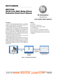
NCV7240EVB
NCV7240
Octal Low-Side Relay Driver
Evaluation Board User's Manual
http://onsemi.com
EVAL BOARD USER’S MANUAL
Description
Features
The NCV7240 evaluation board provides a convenient
method to evaluate the NCV7240 octal low-side driver in a
customer defined application environment.
The setup involves the use of a PC installed with custom
designed software, an interface board, and the NCV7240
evaluation board. The evaluation board is controlled using
the ON Semiconductor FlexMOS GUI installed on a
personal computer (PC). The USB to SPI interface adapter
board provides master-slave communication between the
target demonstration board and the PC.
The user can control each of the eight low-side outputs
independently using this system setup.
The evaluation board’s power management includes an
adjustable LDO giving the option for a 3.3 V or 5 V digital
supply voltage (VCC) selectable through the GUI. An
external power supply can be used by removing a jumper on
the board. Visual indicators dictate the board configuration
through LEDs.
•
•
•
•
•
•
•
8 Channels
600 mA Low−Side Drivers
Programmable Logic Supply Voltage
16−bit SPI Control
Over Load and Over Temperature Protection
Selectable Open Load Detection for LED Loads
Dedicated GUI Interface for Device Control and
Diagnostic
Figure 1. Evaluation Board Solution
© Semiconductor Components Industries, LLC, 2012
April, 2012 − Rev. 0
1
Publication Order Number:
EVBUM2052/D
NCV7240EVB
Figure 2. Evaluation Board
Table 1. ABSOLUTE MAXIMUM RATINGS
Value
Units
Main Supply Voltage to output pins (OUTx)
Rating
−0.3 to 36
V
Digital Supply Voltage (VCC)
−0.3 to 5.5
V
USB to SPI Interface Adapter Connector Pins
−0.5 to 5.5
V
Junction Temperature (NCV7240)
−40 to 150
°C
Ambient Temperature (Evaluation board)
−40 to 105
°C
Stresses exceeding Maximum Ratings may damage the device. Maximum Ratings are stress ratings only. Functional operation above the
Recommended Operating Conditions is not implied. Extended exposure to stresses above the Recommended Operating Conditions may affect
device reliability.
Table 2. RECOMMENDED OPERATING CONDITIONS
Rating
Units
Value
Min
Max
External Digital Supply Voltage (VCC)
3.0
5.5
V
Main Supply Voltage (VBAT)
5.5
28
V
−
0.6
A
−40
125
°C
DC Output Current
Junction Temperature
http://onsemi.com
2
NCV7240EVB
Table 3. PIN FUNCTION DESCRIPTION
Connector
Pin Number
Terminal Name
24 Pin Interface
Connector
1
SCL
I2C Clock Line, 3.3 V Levels
Description
2
SDA
I2C Data Line, 3.3 V Levels
3
GND
Ground
4
GND
Ground
5
IN4
General-Purpose Output 7, used for parallel control of OUT4 and OUT8
6
PO6
General-Purpose Output 6
7
IN3
General-Purpose Output 5, used for parallel control of OUT3 and OUT7
8
V5_EN
9
IN2
General-Purpose Output 3, used for parallel control of OUT2 and OUT6
10
IN1
General-Purpose Output 2, used for parallel control of OUT1 and OUT5
11
EN
General-Purpose Output 1, used for EN, Chip Enable
12
LHI
General-Purpose Output 0, used for Limp−Home Logic input
13
GND
Ground
14
GND
Ground
15
PI1
General-Purpose Input 1
16
PI0
General-Purpose Input 0
17
VIO
3.3 V or 5 V for level translators
18
PI2
General-Purpose Input 2
19
SO
SPI data from slave to master
20
SI
SPI data from master to slave
21
SCLK
SPI clock from master to slave
22
CSB
SPI slave chip select bar
23
VTRGT
24
VCC_USB
General-Purpose Output 4, used for controlling the LDO reference
5 V Supply from slave to J1
5 V USB voltage from the USB to SPI adapter board to the evaluation board
(100 mA max)
Supply
Requirement
VBAT
Main Supply Voltage. Powers the NCV7240 drivers and the onboard LDO.
GND
Ground
Low_Side
Driver Outputs
OUT1
Low−Side Output 1
OUT2
Low−Side Output 2
OUT3
Low−Side Output 3
OUT4
Low−Side Output 4
OUT5
Low−Side Output 5
OUT6
Low−Side Output 6
OUT7
Low−Side Output 7
OUT8
Low−Side Output 8
http://onsemi.com
3
NCV7240EVB
Table 3. PIN FUNCTION DESCRIPTION
Connector
Name
Test Points &
LED Indicator
V5_EN
Supply
Disconnect
EN
Description
When this signal is high the LDO is programmed for 5 V output.
Enable signal for the integrated driver. EN LED is illuminated when the part is enabled.
TSD
Latched thermal information.
LHI
Limp−Home Logic Input.
IN1
Parallel input 1 used for parallel control of OUT1 and OUT5.
An LED is illuminated when the pin is high.
IN2
Parallel input 2 used for parallel control of OUT2 and OUT6.
An LED is illuminated when the pin is high
IN3
Parallel input 3 used for parallel control of OUT3 and OUT7.
An LED is illuminated when the pin is high.
IN4
Parallel input 4 used for parallel control of OUT4 and OUT8.
An LED is illuminated when the pin is high.
CSB
Chip Select Bar signal produced by the master.
CSB LED is illuminated when CSB transition to a low state.
SCLK
Serial clock signal generated by the master.
SI
Serial input data from the master.
SO
Serial output data from the slave.
VCC
Digital Supply voltage. VCC LED is illuminated when the LDO is regulating.
GND
Chip Ground
J28
J28 disconnects the VBAT supply from the board.
No power is delivered to the LDOs when the jumper is disconnected.
J29
J29 disconnects VDD supply from the LDO to the board. When the jumper is disconnected, the
board can be powered from an external supply.
J31
J31 disconnects VDDA supply from the LDO to the board. When the jumper is disconnected,
the board can be powered from an external supply.
http://onsemi.com
4
NCV7240EVB
OPERATIONAL GUIDELINES
The material necessary to successfully use the evaluation
boards is listed below:
• PC running the latest Onsemi FlexMOS GUI
• USB cable Type A to Type B
• USB to SPI Interface Adapter with Ribbon Cable
• NCV7240 Evaluation Board
• Power Supply
• Resistive, LED, Inductive or Motor Load
An application example of the NCV7240 driving relays is
shown in Figure 3. Figure 3 shows J28, J29 and J31 jumpers
inserted. This powers the on-board LDO regulators for VDD
and VDDA. Both VDD and VDDA light their respective
LED (D10 and D11) when powered. The multiple VBAT
connectors on the terminal blocks help the user connect
loads in the system by providing a connection which
provides capability for two wires per terminal site.
When VBAT voltage is applied to the board, the onboard
regulator regulates the VDD voltage. By default, VCC is
regulated to 3.3 V, but this can be adjusted to 5 V via the GUI.
VCC power to the board is provided via VDDA through
R20 and is shown active with diode D2.
14V
Figure 3. Application Example
device from the drop down box. If the device name doesn’t
appear in the drop down box, the latest version of the GUI
needs to be installed on the PC.
A detailed description of the GUI functionality for the
NCV7240 is shown in Figure 4. The FlexMOS GUI is used
to enable or disable the device and to control the low−side
driver outputs.
Once the hardware is configured with the desired load and
is interfaced with the USB to SPI adapter, the user can launch
the FlexMOS software. Once the software is running, the
GUI should automatically identify the connected
demonstration board and load the appropriate GUI interface
for the low-side drivers. If the software doesn’t recognize
the connected demonstration board, manually select the
http://onsemi.com
5
NCV7240EVB
Figure 4. GUI Overview
http://onsemi.com
6
NCV7240EVB
TYPICAL CHARACTERISTICS
Figure 5. Typical Output Clamping Action
Typical Operation
a multiple of 8 [16 bit minimum]) is reported on the SO pin
after CSB goes low until the first rising edge of SCLK.
Detection can be performed by clicking on the TER button
in the GUI.
Since SI is OR’d with the TER fault, it is important to
understand that if the LSB bit (B0) is set high on the previous
frame, the TER should be ignored. This is because SI holds
the value of B0 until the first SCLK rising edge and TER is
latched in before the first rising edge of SCLK.
Figure 5 above highlights the clamping action (clamped
to 38.2 V) of the NCV7240 as the device turns off when
driving an inductive load. In this case, a relay has turned off.
The slight hump in the decaying waveform is caused from
the mechanical relay action of the system.
Transmission Error (TER)
The NCV7240 device includes a transmission error
detection feature whereby a transmission error (bit count not
VDDA
VBAT
VDD
1
C1
0.1uF
1
J3
J6
J9
VBAT
J7
19
22
20
23
SO
SI
SCLK
CSB
14
15
16
17
LHI
EN
OUT1
OUT2
OUT3
OUT4
OUT5
OUT6
OUT7
OUT8
SO
SI
SCLK
CSB
IN4
IN3
IN2
IN1
C3
0.1uF
Opt
C4
0.1uF
Opt
J10
D1
C11
0.1uF
IN
GND
NC
VCC
OUT
SO LED
NL17SH04
5
4
2
1
2
1
2
1
C7
0.1uF
Opt
C8
0.1uF
Opt
C9
0.1uF
Opt
C10
0.1uF
Opt
TER
620
0Ohm
R26
2 Ohm
R2
R4
200Ohm
C23
0.1uF
J32
C22
0.1uF
R1
U3
1
2
3
C6
0.1uF
Opt
1
TER
R3
C5
0.1uF
Opt
Vcc
Vcc
0Ohm
2
1
3
4
5
6
7
8
9
10
1
2
11
12
IN4
IN3
IN2
IN1
NCV7240
1
2
3
4
5
6
7
QA VDD
QB
QA
QB
CA
CB
RA
RB
DA
DB
SA
VSS SB
MC14013B
Figure 6. Evaluation Board (DUT)
http://onsemi.com
7
Vcc
U2
14
13
12
11
10
9
8
2
1
18
21
LHI
EN
VDDA
VDD
2
1
24
13
GND
GND
GND
GND
2
1
C2
0.1uF
CSB
J5
U1
NCV7240
J8
HOSTPWR
J4
2
1
J2
J1
C12
0.1uF
NCV7240EVB
IN1
IN2
IN3
IN4
EN
LHI
CSB
20
2
3
4
5
6
7
8
9
11
1
D1
D2
D3
D4
D5
D6
D7
D8
C13
0.1uF
U4
MM74HC573/SOEIAJ
19
Q1 18
Q2 17
Q3 16
Q4 15
Q5 14
Q6 13
Q_CSB
Q7 12
Q_VCC
Q8
LE
OC
D3
D2
LED
Q_CSB
LED
Q_VCC
10
Vcc
Vcc
VCC
1
1
1
1
1
1
1
R5
R6
R9
R8
R7
R10
R11
GND
J11
J12
J14
J13
J17
J16
J15
0Ohm
0Ohm
0Ohm
0Ohm
0Ohm
0Ohm
0Ohm
R14
620
Vcc
1
SI
J26
1
D4
SI
1
24
22
20
18
16
14
12
10
8
6
4
2
VCC_USB
SS
CSB
PI2
TER
LHI
IN1
V5_EN
LHI
IN1
V3p3_EN
PO6
SDA
23
21
19
17
15
13
11
9
7
5
3
1
D7
D6
D5
LED
VTRGT
J18
J19
J20
J22
J25
LED
LED
LED
D8
LED
D9
1
1
1
1
1
LED
SCLK
SO
SO
VIO
PI1
EN
IN2
IN3
IN4
R19
620
J21
J24
J23
R18
620
R17
620
R15
620
1
J27
EN
IN2
IN3
IN4
Vcc
SCL
VDDA
R20
0Ohm
U5 AT24C01A
1
2
3
SCL
6
7
8
VCC_USB
A0
A1
A2
SDA
5
SDA
SCL
WP
VCC
C14
0.1uF
Figure 7. Evaluation Board (Interface)
JUMPER
JUMPER
C16
1uF
Vin
INH
VOUT
VA
1 J29
C17
1uF
3
6
C15
100nF
5
4
GND
TAB
1
2
VIN
C18
22uF
D10
LED
R22
14.7k
M1
V5_EN
V5_EN
MGSF1N02LT1
1
J30
U7
NCV4274
1
C20
100nF
C21
1uF
VIN
GND
TAB
2
JUMPER
VOUT
3
1 J31
C19
22uF
2
4
VBAT
1 J28
D11
Figure 8. Evaluation Board (Power)
http://onsemi.com
8
LED
2
VDDA
2
VDD
NCV7240EVB
Bill of Materials (NCV7240 Evaluation Board)
http://onsemi.com
9
NCV7240EVB
EVALUATION BOARD LAYOUT
Figure 9. Silk Screen & Drill Holes
Figure 10. Top Copper
Figure 11. Bottom Copper
Figure 12. Board Composite
http://onsemi.com
10
NCV7240EVB
ON Semiconductor and
are registered trademarks of Semiconductor Components Industries, LLC (SCILLC). SCILLC reserves the right to make changes without further notice
to any products herein. SCILLC makes no warranty, representation or guarantee regarding the suitability of its products for any particular purpose, nor does SCILLC assume any liability
arising out of the application or use of any product or circuit, and specifically disclaims any and all liability, including without limitation special, consequential or incidental damages.
“Typical” parameters which may be provided in SCILLC data sheets and/or specifications can and do vary in different applications and actual performance may vary over time. All
operating parameters, including “Typicals” must be validated for each customer application by customer’s technical experts. SCILLC does not convey any license under its patent rights
nor the rights of others. SCILLC products are not designed, intended, or authorized for use as components in systems intended for surgical implant into the body, or other applications
intended to support or sustain life, or for any other application in which the failure of the SCILLC product could create a situation where personal injury or death may occur. Should
Buyer purchase or use SCILLC products for any such unintended or unauthorized application, Buyer shall indemnify and hold SCILLC and its officers, employees, subsidiaries, affiliates,
and distributors harmless against all claims, costs, damages, and expenses, and reasonable attorney fees arising out of, directly or indirectly, any claim of personal injury or death
associated with such unintended or unauthorized use, even if such claim alleges that SCILLC was negligent regarding the design or manufacture of the part. SCILLC is an Equal
Opportunity/Affirmative Action Employer. This literature is subject to all applicable copyright laws and is not for resale in any manner.
PUBLICATION ORDERING INFORMATION
LITERATURE FULFILLMENT:
Literature Distribution Center for ON Semiconductor
P.O. Box 5163, Denver, Colorado 80217 USA
Phone: 303−675−2175 or 800−344−3860 Toll Free USA/Canada
Fax: 303−675−2176 or 800−344−3867 Toll Free USA/Canada
Email: [email protected]
N. American Technical Support: 800−282−9855 Toll Free
USA/Canada
Europe, Middle East and Africa Technical Support:
Phone: 421 33 790 2910
Japan Customer Focus Center
Phone: 81−3−5817−1050
http://onsemi.com
11
ON Semiconductor Website: www.onsemi.com
Order Literature: http://www.onsemi.com/orderlit
For additional information, please contact your local
Sales Representative
EVBUM2052/D


