1
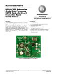
NCV7718EVB, NCV7720EVB
NCV7718, NCV7720
Half-Bridge Drivers
Evaluation Board User's
Manual
http://onsemi.com
EVAL BOARD USER’S MANUAL
Description
Features
The NCV7717-7720 evaluation board provides a
convenient method to evaluate the NCV7718 and NCV7720
half-bridge drivers in a suitable application environment. A
one board solution for all the drivers in the family is possible
since all the devices share the same package and common
pin-out structure. The evaluation board is intended to be
used with the ON Semiconductor FlexMOS GUI installed
on a personal computer (PC) and the USB to SPI interface
adapter board for a master-slave communication between
the target board and the PC. The evaluation boards allow
flexible configuration of the various loads and each of the
half-bridges can be individually controlled via the FlexMOS
GUI. The evaluation board is populated with an adjustable
LDO (NCV4276), so a 3.3 V or 5 V digital supply voltage
(VCC) can be selected through the GUI. By means of a
jumper the user can bypass the onboard regulator and use an
external power supply. Furthermore the onboard LEDs
provide visual indication of the board configuration. An
external reverse battery circuitry is implemented on the
evaluation board to protect the integrated driver in scenarios
where the VBAT supply polarity is reversed. This feature
can be disabled by slightly modifying the board.
• One Hardware Solution for NCV7718 and NCV7720
Half−Bridge Drivers
• 0.55 A Peak Current
• High Side and Low Side Drivers Connected as
Half-Bridge Configuration
• Rdson = 1 W (typ)
• 3.3 V or 5 V VCC Operation with an Onboard
Adjustable Regulator
• Over Current and Over Temperature Protection
• Under Load Detection
• Dedicated GUI Interface for Device Control and
Diagnostic
Figure 1. FlexMOS Evaluation Board Solution
© Semiconductor Components Industries, LLC, 2012
February, 2012 − Rev. 2
1
Publication Order Number:
EVBUM2048/D
NCV7718EVB, NCV7720EVB
Half−Bridge Outputs
24 Pin Interface Connector
Supply Requirements
Test Points
Ground Bus Wire
LED Indicators
Supply Disconnect
Figure 2. Evaluation Board
Table 1. ABSOLUTE MAXIMUM RATINGS
Rating
Value
Units
Main Supply Voltage (VBAT)
Without Reverse Battery Protection Circuitry
With Reverse Batter Protection Circuitry
−0.3 to 40
−60 to 40
V
External Digital Supply Voltage (VCC)
−0.3 to 5.5
Output Pins (OUTx)
Without Reverse Battery Protection Circuitry
With Reverse Batter Protection Circuitry
−0.3 to 40
−60 to 40
USB to SPI Interface Adapter Connector Pins
−0.5 to 5.5
V
Junction Temperature (NCV7718, NCV7720)
−40 to 150
°C
Ambient Temperature (Evaluation board)
−40 to 105
°C
V
V
Stresses exceeding Maximum Ratings may damage the device. Maximum Ratings are stress ratings only. Functional operation above the
Recommended Operating Conditions is not implied. Extended exposure to stresses above the Recommended Operating Conditions may affect
device reliability.
Table 2. RECOMMENDED OPERATING CONDITIONS
Rating
Units
Value
Min
Max
External Digital Supply Voltage (VCC)
3.15
5.25
V
Main Supply Voltage (VBAT)
5.5
DC Output Current (Per Channel)
Junction Temperature
−40
http://onsemi.com
2
28
V
0.55
A
125
°C
NCV7718EVB, NCV7720EVB
Table 3. PIN FUNCTION DESCRIPTION
Connector
Pin Number
Terminal Name
24 Pin Interface
Connector
1
SCL
I2C Clock Line, 3.3 V Levels
2
SDA
I2C Data Line, 3.3 V Levels
3
GND
Ground
4
GND
Ground
5
PO7
General-Purpose Output 7
6
PO6
General-Purpose Output 6
7
PO5
General-Purpose Output 5
8
PO4
General-Purpose Output 4, used for controlling the LDO reference
9
PO3
General-Purpose Output 3
10
PO2
General-Purpose Output 2
11
PO1
General-Purpose Output 1, used for EN, Chip Enable
12
PO0
General-Purpose Output 0
13
GND
Ground
14
GND
Ground
15
PI1
General-Purpose Input 1, used for reading latched thermal shutdown (TSD)
data
16
PI0
General-Purpose Input 0
17
VIO
3.3 V or 5 V for level translators
18
PI2
General-Purpose Input 2
19
SO
SPI data from slave to master
20
SI
SPI data from master to slave
21
SCLK
SPI clock from master to slave
22
CSB
SPI slave chip select bar
23
VTRGT
24
VCC_USB
5 V USB voltage from the USB to SPI adapter board to the demonstration
board (100 mA max)
VBAT
Main Supply Voltage. Powers the NCV77xx drivers and the onboard LDO.
Supply
Requirement
Half−Bridge
Outputs
(Note 1)
GND_M
Description
5 V Supply from slave to J1
Module Ground
VCC
Optional external digital supply (used only when the onboard LDO is disconnected via VCC_DIS jumper)
OUT1
Half Bridge Output 1
OUT2
Half Bridge Output 2
OUT3
Half Bridge Output 3
OUT4
Half Bridge Output 4
OUT5
Half Bridge Output 5
OUT6
Half Bridge Output 6
OUT7
Half Bridge Output 7
OUT8
Half Bridge Output 8
OUT9
Half Bridge Output 9
OUT10
Half Bridge Output 10
http://onsemi.com
3
NCV7718EVB, NCV7720EVB
Table 3. PIN FUNCTION DESCRIPTION
Connector
Test Points
Name
V5_EN
EN
Enable signal for the integrated driver.
Latched thermal information.
(Note 2)
CSB
Chip Select Bar signal produced by the master. CSB LED is illuminated when CSB transition to
a low state.
SCLK
Serial clock signal generated by the master.
SI
Serial input data from the master.
SO
Serial output data from the slave
VCC
GND
Supply
Disconnect
When this signal is high the LDO is programmed for 5 V output.
TSD
V_USB
LED Indicator
Description
EN
Digital Supply voltage.
Supply voltage from the USB port.
Chip Ground
EN LED is illuminated when the part is enabled.
TSD
TSD LED is illuminated when part encountered a latched thermal shutdown.
(Note 2)
CSB
CSB LED is illuminated when CSB transition to a low state.
VCC
VCC LED is illuminated when the LDO is regulating.
VCC_REG
VCC_REG LED is illuminated when the regulated voltage is applied to the demonstration
board.
VBAT_DIS
VBAT_DIS jumper is used to disconnect the VBAT supply from the board. No power is delivered
to the integrated driver or the LDO when the jumper is disconnected.
VCC_DIS
VCC_DIS jumper is used to disconnect the VCC supply from the LDO to the board. When the
jumper is disconnected the board can be powered from an external supply.
1. OUT7 − OUT10 are only available in NCV7720 devices.
2. SI is OR’ed with the TSD fault, so if the LSB bit (B0) is set high on the previous frame the TSD will be set high.
http://onsemi.com
4
NCV7718EVB, NCV7720EVB
OPERATIONAL GUIDELINES
The material necessary to successfully use the
demonstration boards is given hereunder:
• PC running the latest Onsemi FlexMOS GUI
• USB cable Type A to Type B
• USB to SPI Interface Adapter with Ribbon Cable
• NCV7717-7720 Evaluation Board
• Power Supply
• Resistive, Inductive or Motor Load
An application example of a NCV7720 driving motor
loads is given in Figure 3. The same concept can be applied
to the rest of the half-bridge integrated drivers in the family
and for different load types.
Figure 3 shows the VCC_DIS and the VBAT_DIS
jumpers inserted, so the digital supply and battery voltage is
applied to the board. When VBAT voltage is applied to the
board, the onboard regulator regulates the VCC voltage. By
default the VCC is regulated to 3.3 V, but this can be adjusted
to 5 V via the GUI. The onboard LED VCC_REG is
illuminated when the regulator is active. If the VCC power
is delivered to the board (VCC_DIS is closed) the VCC LED
is also activated.
MOTOR 4
MOTOR 2
12V
MOTOR 5
MOTOR 3
MOTOR 1
Figure 3. Application Example
The FlexMOS GUI is used to enable or disable the device
and to control the half−bridge outputs. For the application
example given in Figure 3, the motor 1 is driven in the
forward direction by enabling the high side power
MOSFTET on OUT1 and the low side power MOSFET on
OUT5. Conversely the current can be directed to flow in the
reverse direction by enabling the low side power MOSFTET
on OUT1 and the high side power MOSFET on OUT5. The
same methodology can be carried out for the subsequent
motor operations by controlling their respective outputs.
Once the hardware is configured with the desired load and
is interfaced with the USB to SPI adapter, the user can
invoke the FlexMOS software. Once the software is
launched the GUI should automatically identify the
connected demonstration board and loads the appropriate
GUI interface for the half-bridge driver. If the software
doesn’t recognize the connected demonstration board,
manually select the device from the drop down box. If the
device name doesn’t appear in the drop down box, the latest
version of the GUI needs to be installed on the PC.
A detailed description of the GUI functionality for the
NCV7718 is provided in Figure 4.
http://onsemi.com
5
Half−Bridge Control
6
SPI Traffic
Status Info
http://onsemi.com
Figure 4. GUI Overview
Enable Device: Enables or disables the integrated driver
Status Reset: Resets all latched faults
Under Load Shutdown: Enables or disables ULDSC feature
Overvoltage Lockout: Enables or disabled OVLO feature
Check Box Control
Update: Transmits the compiled SPI-Frame to the slave device
All LS ON: Selects LS ON for all the half-bridge outputs
ALL HS ON: Selects HS ON for all the half-bridge outputs
ALL OFF: Selects OFF for all the half-bridge outputs
TSD: Creates a CSB pulse with no clock to for latched thermal
information.
Push Button Control
Log of SPI command send and received.
Reports all global faults
Programs the onboard LDO for either 3.3V or 5V operation.
VCC Mode
Manual: User must press Update" button for any changes
made to Half-Bridge Control to be take effect.
Auto: When the Half-Bridge Control is changed the Update"
button is automatically triggered.
Polling: The Half-Bridge Control is updated periodically at a
predefined interval.
GUI update Mode
Compiled SPI frame based on the Half-Bridge Control input
Compiled SPI−Frame
Reports whether the half-bridge is in tri-state, LS or HS
enabled.
Half−Bridge Status
Allows independent control of the half-bridges
Half−Bridge Status
Half−Bridge Control
NCV7718EVB, NCV7720EVB
NCV7718EVB, NCV7720EVB
TYPICAL CHARACTERICTICS
Figure 5. VCC = 3.3 V, LS Configuration Switch
Turn On Resistive Load
Figure 6. VCC = 3.3 V, HS Configuration Switch
Turn On Resistive Load
Figure 7. VCC = 3.3 V, OUT1_OUT5 H−Bridge
Configuration Forward, Reverse, Forward Loop with
a Motor Load
Figure 8. VCC = 3.3 V HVAC Motor Forward
Figure 9. VCC = 3.3 V HVAC Motor Reverse
http://onsemi.com
7
NCV7718EVB, NCV7720EVB
http://onsemi.com
8
NCV7718EVB, NCV7720EVB
Figure 10. Evaluation Board Schematic
BILL OF MATERIAL
Table 4. BILL OF MATERIAL
Ref
Qty
Description
Value
Manufacturer
Manufacturer’s
Part Number
C1–C19,
C23
20
CAP CER .1UF 50V 10% X7R 0805
0.1 uF
Murata Electronics
North America
GRM21BR71H104KA01L
C20, C21
2
CAP CER 1UF 50V X7R 0805
1.0 uF
Murata Electronics
North America
GRM21BR71H105KA12L
C22
1
CAP CER 22UF 16V X5R 1206
22 uF
Murata Electronics
North America
GRM31CR61C226ME15L
D1–D6
6
LED GREEN CLEAR THIN 0805 SMD
N/A
Lite-On Inc
LTST-C171GKT
D7
1
DIODE SWITCH 75V 200MA SOT-23
N/A
ON Semiconductor
BAS16LT3G
J1, J2, J4,
J6, J7, J8,
J9
7
CONN TERM BLOCK 2POS 5.08MM
PCB
N/A
Phoenix Contact
1729128
J3, J5,
J10–J19,
J21, J22,
J25–J33
23
TEST POINT PC MULTI PURPOSE
RED
N/A
Keystone Electronics
5010
J20
1
CONN HEADER VERT 24POS .100
GOLD
N/A
TE Connectivity
5499910-5
J23, J24
2
CONN HEADER 2POS .100 VERT
GOLD
N/A
Molex Connector
Corporation
22-28-4024
http://onsemi.com
9
NCV7718EVB, NCV7720EVB
Table 4. BILL OF MATERIAL
Ref
Qty
Description
Value
Manufacturer
Manufacturer’s
Part Number
M1
1
MOSFET N-CH 20V 750MA SOT23
20 V /
0.75 A
ON Semiconductor
MGSF1N02LT1G
Q1
1
MOSFET N-CH 60V 24A DPAK
60 V /
24 A
ON Semiconductor
NTD24N06LT4G
R1, R8, R9,
R10, R11,
R15
6
RES 620 OHM 1/8W 1% 0805 SMD
620
Vishay/Dale
CRCW0805620RFKEA
R2, R3, R6,
R7
4
RES 0.0 OHM 1/10W 0603 SMD
0
Panasonic- ECG
ERJ-3GEY0R00V
R4
1
RES 2.00 OHM 1/8W 1% 0805 SMD
2
Vishay/Dale
CRCW08052R00FKEA
R5
1
RES 200 OHM 1/8W 1% 0805 SMD
200
Vishay/Dale
CRCW0805200RFKEA
R12
1
RES 10.0K OHM 1/8W 1% 0805 SMD
10.0 K
Vishay/Dale
CRCW080510K0FKEA
R13
1
RES 14.7K OHM 1/8W 1% 0805 SMD
14.7 K
Vishay/Dale
CRCW080514K7FKEA
R14
1
RES 30.9K OHM 1/8W 1% 0805 SMD
30.9 K
Vishay/Dale
CRCW080530K9FKEA
R16
1
RES 22.0K OHM 1/8W 1% 0805 SMD
22 K
Vishay/Dale
CRCW080522K0FKEA
R17–R22
6
RES 0.0 OHM 1/8W 0805 SMD
0
Vishay/Dale
CRCW08050000Z0EA
U1
1
Half−Bridge Driver
N/A
ON Semiconductor
NCV77XX
U2
1
IC FLIP-FLOP DUAL CMOS 14SOIC
N/A
ON Semiconductor
MC14013BDR2G
U3
1
Single Inverter
N/A
ON Semiconductor
NL17SH04P5T5G
U4
1
IC LATCH OCTAL D 3STATE 20-TSSOP
N/A
ON Semiconductor
MM74HC573MTC
U5
1
IC EEPROM 1KBIT 1MHZ 8SOIC
N/A
Atmel
AT24C01BN-SH-B
U6
1
IC REG LDO 400MA ADJ D-PAK
N/A
ON Semiconductor
NCV4276BDTADJRKG
EVALUATION BOARD FEATURES
Reverse Battery Protection
Latched Thermal Information
The reverse battery protection scheme is employed as
shown in the bottom section of Figure 10.
An N-channel NTD24N06L MOSFET is used to isolate
the chip ground of the integrated driver from the module
ground. When proper VBAT voltage is applied to the gate,
the MOSFET will be pulled up to the regulated VCC
voltage. Thus turning on the MOSFET and connecting the
module ground and the chip ground via a very low ohmic
drop. Even when the LDO is not regulating (in absence of
gate voltage to the MOSFET) there is a current path from
VBAT to the module ground through the inherent body
diode of the MOSFET. In cases where the polarity of the
VBAT supply voltage is reversed the MOSFET will not
conduct and the module ground will be disconnected from
the chip ground.
The reverse battery protection can be disabled by
depopulating resistors: R20, R21 and R22 and shorting the
following resistors: R17, R18 and R19.
When the TSD button is pressed on the FlexMOS GUI,
latched thermal shutdown information is monitored on the
demonstration board through the TSD LED indicator (D1).
Since the SI is OR’ed with the TSD fault it is important to
understand that if the LSB bit (B0) is set high on the previous
frame the TSD reporting should be ignored. This is because
SI holds the value of B0 until the first SCLK rising edge and
the TSD information is latched in before the first rising edge
of SCLK.
http://onsemi.com
10
NCV7718EVB, NCV7720EVB
EVALUATION BOARD LAYOUT
Figure 11. Silk Screen & Drill Holes
Figure 12. Top Copper
Figure 13. Bottom Copper
Figure 14. Board Composite
http://onsemi.com
11
NCV7718EVB, NCV7720EVB
ON Semiconductor and
are registered trademarks of Semiconductor Components Industries, LLC (SCILLC). SCILLC reserves the right to make changes without further notice
to any products herein. SCILLC makes no warranty, representation or guarantee regarding the suitability of its products for any particular purpose, nor does SCILLC assume any liability
arising out of the application or use of any product or circuit, and specifically disclaims any and all liability, including without limitation special, consequential or incidental damages.
“Typical” parameters which may be provided in SCILLC data sheets and/or specifications can and do vary in different applications and actual performance may vary over time. All
operating parameters, including “Typicals” must be validated for each customer application by customer’s technical experts. SCILLC does not convey any license under its patent rights
nor the rights of others. SCILLC products are not designed, intended, or authorized for use as components in systems intended for surgical implant into the body, or other applications
intended to support or sustain life, or for any other application in which the failure of the SCILLC product could create a situation where personal injury or death may occur. Should
Buyer purchase or use SCILLC products for any such unintended or unauthorized application, Buyer shall indemnify and hold SCILLC and its officers, employees, subsidiaries, affiliates,
and distributors harmless against all claims, costs, damages, and expenses, and reasonable attorney fees arising out of, directly or indirectly, any claim of personal injury or death
associated with such unintended or unauthorized use, even if such claim alleges that SCILLC was negligent regarding the design or manufacture of the part. SCILLC is an Equal
Opportunity/Affirmative Action Employer. This literature is subject to all applicable copyright laws and is not for resale in any manner.
PUBLICATION ORDERING INFORMATION
LITERATURE FULFILLMENT:
Literature Distribution Center for ON Semiconductor
P.O. Box 5163, Denver, Colorado 80217 USA
Phone: 303−675−2175 or 800−344−3860 Toll Free USA/Canada
Fax: 303−675−2176 or 800−344−3867 Toll Free USA/Canada
Email: [email protected]
N. American Technical Support: 800−282−9855 Toll Free
USA/Canada
Europe, Middle East and Africa Technical Support:
Phone: 421 33 790 2910
Japan Customer Focus Center
Phone: 81−3−5817−1050
http://onsemi.com
12
ON Semiconductor Website: www.onsemi.com
Order Literature: http://www.onsemi.com/orderlit
For additional information, please contact your local
Sales Representative
EVBUM2048/D