1
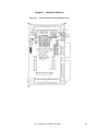
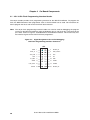
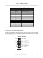
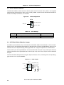
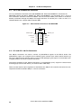
User’s Manual
MC-CPU-78F0714
Micro-Board for µPD78F0714 Microcontroller
for use with Motor Control I/O Interface Board
Document No. U17707EU1V1UME0
Date Published August 2006
© NEC Electronics Corporation 2006
Printed in Germany
CAUTION
This is a Test- and Measurement equipment with possibility to be
significantly altered by user through hardware enhancements/modifications
and/or test or application software. Thus, with respect to Council Directive
89/336/EEC (Directive on compliance with the EMC protection
requirements), this equipment has no autonomous function. Consequently
this equipment is not marked by the CE-symbol.
EEDT-ST-0005-10
Redemption of Waste Electrical and Electronic Equipment
(WEEE) in accordance with legal regulations applicable in
the European Union only: This equipment (including all
accessories) is not intended for household use. After use
the equipment cannot be disposed of as household waste.
NEC Electronics (Europe) GmbH offers to take back the
equipment. All you need to do is register at
www.eu.necel.com/weee.
All (other) product, brand, or trade names used in this pamphlet are the trademarks or
registered trademarks of their respective owners.
Product specifications are subject to change without notice. To ensure that you have
the latest product data, please contact your local NEC Electronics sales office.
2
User’s Manual U17707EU1V1UME0
NOTES FOR CMOS DEVICES
1
VOLTAGE APPLICATION WAVEFORM AT INPUT PIN
Waveform distortion due to input noise or a reflected wave may cause malfunction. If the input of the
CMOS device stays in the area between VIL (MAX) and VIH (MIN) due to noise, etc., the device may
malfunction. Take care to prevent chattering noise from entering the device when the input level is fixed,
and also in the transition period when the input level passes through the area between VIL (MAX) and
VIH (MIN).
2
HANDLING OF UNUSED INPUT PINS
Unconnected CMOS device inputs can be cause of malfunction. If an input pin is unconnected, it is
possible that an internal input level may be generated due to noise, etc., causing malfunction. CMOS
devices behave differently than Bipolar or NMOS devices. Input levels of CMOS devices must be fixed
high or low by using pull-up or pull-down circuitry. Each unused pin should be connected to VDD or GND
via a resistor if there is a possibility that it will be an output pin. All handling related to unused pins must
be judged separately for each device and according to related specifications governing the device.
3
PRECAUTION AGAINST ESD
A strong electric field, when exposed to a MOS device, can cause destruction of the gate oxide and
ultimately degrade the device operation. Steps must be taken to stop generation of static electricity as
much as possible, and quickly dissipate it when it has occurred. Environmental control must be
adequate. When it is dry, a humidifier should be used. It is recommended to avoid using insulators that
easily build up static electricity. Semiconductor devices must be stored and transported in an anti-static
container, static shielding bag or conductive material. All test and measurement tools including work
benches and floors should be grounded. The operator should be grounded using a wrist strap.
Semiconductor devices must not be touched with bare hands. Similar precautions need to be taken for
PW boards with mounted semiconductor devices.
4
STATUS BEFORE INITIALIZATION
Power-on does not necessarily define the initial status of a MOS device. Immediately after the power
source is turned ON, devices with reset functions have not yet been initialized. Hence, power-on does
not guarantee output pin levels, I/O settings or contents of registers. A device is not initialized until the
reset signal is received. A reset operation must be executed immediately after power-on for devices
with reset functions.
5
POWER ON/OFF SEQUENCE
In the case of a device that uses different power supplies for the internal operation and external
interface, as a rule, switch on the external power supply after switching on the internal power supply.
When switching the power supply off, as a rule, switch off the external power supply and then the
internal power supply. Use of the reverse power on/off sequences may result in the application of an
overvoltage to the internal elements of the device, causing malfunction and degradation of internal
elements due to the passage of an abnormal current.
The correct power on/off sequence must be judged separately for each device and according to related
specifications governing the device.
6
INPUT OF SIGNAL DURING POWER OFF STATE
Do not input signals or an I/O pull-up power supply while the device is not powered. The current
injection that results from input of such a signal or I/O pull-up power supply may cause malfunction and
the abnormal current that passes in the device at this time may cause degradation of internal elements.
Input of signals during the power off state must be judged separately for each device and according to
related specifications governing the device.
User’s Manual U17707EU1V1UME0
3
• The information in this document is current as of August, 2006. The information is subject to
change without notice. For actual design-in, refer to the latest publications of NEC Electronics data
sheets or data books, etc., for the most up-to-date specifications of NEC Electronics products. Not
all products and/or types are available in every country. Please check with an NEC Electronics sales
representative for availability and additional information.
• No part of this document may be copied or reproduced in any form or by any means without the prior
written consent of NEC Electronics. NEC Electronics assumes no responsibility for any errors that may
appear in this document.
• NEC Electronics does not assume any liability for infringement of patents, copyrights or other intellectual
property rights of third parties by or arising from the use of NEC Electronics products listed in this document
or any other liability arising from the use of such products. No license, express, implied or otherwise, is
granted under any patents, copyrights or other intellectual property rights of NEC Electronics or others.
• Descriptions of circuits, software and other related information in this document are provided for illustrative
purposes in semiconductor product operation and application examples. The incorporation of these
circuits, software and information in the design of a customer's equipment shall be done under the full
responsibility of the customer. NEC Electronics assumes no responsibility for any losses incurred by
customers or third parties arising from the use of these circuits, software and information.
• While NEC Electronics endeavors to enhance the quality, reliability and safety of NEC Electronics products,
customers agree and acknowledge that the possibility of defects thereof cannot be eliminated entirely. To
minimize risks of damage to property or injury (including death) to persons arising from defects in NEC
Electronics products, customers must incorporate sufficient safety measures in their design, such as
redundancy, fire-containment and anti-failure features.
• NEC Electronics products are classified into the following three quality grades: "Standard", "Special" and
"Specific".
The "Specific" quality grade applies only to NEC Electronics products developed based on a customerdesignated "quality assurance program" for a specific application. The recommended applications of an NEC
Electronics product depend on its quality grade, as indicated below. Customers must check the quality grade of
each NEC Electronics product before using it in a particular application.
"Standard": Computers, office equipment, communications equipment, test and measurement equipment, audio
and visual equipment, home electronic appliances, machine tools, personal electronic equipment
and industrial robots.
"Special": Transportation equipment (automobiles, trains, ships, etc.), traffic control systems, anti-disaster
systems, anti-crime systems, safety equipment and medical equipment (not specifically designed
for life support).
"Specific": Aircraft, aerospace equipment, submersible repeaters, nuclear reactor control systems, life
support systems and medical equipment for life support, etc.
The quality grade of NEC Electronics products is "Standard" unless otherwise expressly specified in NEC
Electronics data sheets or data books, etc. If customers wish to use NEC Electronics products in applications
not intended by NEC Electronics, they must contact an NEC Electronics sales representative in advance to
determine NEC Electronics' willingness to support a given application.
(Note)
(1) "NEC Electronics" as used in this statement means NEC Electronics Corporation and also includes its
majority-owned subsidiaries.
(2) "NEC Electronics products" means any product developed or manufactured by or for NEC Electronics (as
defined above).
M8E 02. 11-1
4
User’s Manual U17707EU1V1UME0
For further information,
please contact:
NEC Electronics Corporation
1753, Shimonumabe, Nakahara-ku,
Kawasaki, Kanagawa 211-8668,
Japan
Tel: 044-435-5111
http://www.necel.com/
[America]
[Europe]
[Asia & Oceania]
NEC Electronics America, Inc.
2880 Scott Blvd.
Santa Clara, CA 95050-2554, U.S.A.
Tel: 408-588-6000
800-366-9782
http://www.am.necel.com/
NEC Electronics (Europe) GmbH
Arcadiastrasse 10
40472 Düsseldorf, Germany
Tel: 0211-65030
http://www.eu.necel.com/
NEC Electronics (China) Co., Ltd
7th Floor, Quantum Plaza, No. 27 ZhiChunLu Haidian
District, Beijing 100083, P.R.China
Tel: 010-8235-1155
http://www.cn.necel.com/
Hanover Office
Podbielskistrasse 166 B
30177 Hannover
Tel: 0 511 33 40 2-0
Munich Office
Werner-Eckert-Strasse 9
81829 München
Tel: 0 89 92 10 03-0
Stuttgart Office
Industriestrasse 3
70565 Stuttgart
Tel: 0 711 99 01 0-0
United Kingdom Branch
Cygnus House, Sunrise Parkway
Linford Wood, Milton Keynes
MK14 6NP, U.K.
Tel: 01908-691-133
Succursale Française
9, rue Paul Dautier, B.P. 52180
78142 Velizy-Villacoublay Cédex
France
Tel: 01-3067-5800
Sucursal en España
Juan Esplandiu, 15
28007 Madrid, Spain
Tel: 091-504-2787
NEC Electronics Shanghai Ltd.
Room 2509-2510, Bank of China Tower,
200 Yincheng Road Central,
Pudong New Area, Shanghai P.R. China P.C:200120
Tel: 021-5888-5400
http://www.cn.necel.com/
NEC Electronics Hong Kong Ltd.
12/F., Cityplaza 4,
12 Taikoo Wan Road, Hong Kong
Tel: 2886-9318
http://www.hk.necel.com/
Seoul Branch
11F., Samik Lavied’or Bldg., 720-2,
Yeoksam-Dong, Kangnam-Ku,
Seoul, 135-080, Korea
Tel: 02-558-3737
NEC Electronics Taiwan Ltd.
7F, No. 363 Fu Shing North Road
Taipei, Taiwan, R. O. C.
Tel: 02-8175-9600
http://www.tw.necel.com/
NEC Electronics Singapore Pte. Ltd.
238A Thomson Road,
#12-08 Novena Square,
Singapore 307684
Tel: 6253-8311
http://www.sg.necel.com/
Tyskland Filial
Täby Centrum
Entrance S (7th floor)
18322 Täby, Sweden
Tel: 08 638 72 00
Filiale Italiana
Via Fabio Filzi, 25/A
20124 Milano, Italy
Tel: 02-667541
Branch The Netherlands
Steijgerweg 6
5616 HS Eindhoven
The Netherlands
Tel: 040 265 40 10
G06.8A
User’s Manual U17707EU1V1UME0
5
[MEMO]
6
User’s Manual U17707EU1V1UME0
Preface
Readers
This manual is intented for users who want to understand the functions of the
MC-CPU-78F0714 Micro-Board for µPD78F0714 Microcontroller for use with
Motor Control I/O Interface Board.
Purpose
This manual presents the hardware manual of the MC-CPU-78F0714
Micro-Board for µPD78F0714 Microcontroller for use with Motor Control I/O
Interface Board.
Organization
This system specification describes the following sections:
Legend
•
System specifications
•
Hardware features
•
On-board components
Symbols and notation are used as follows:
Weight in data notation : Left is high-order column, right is low order column
Active low notation
: xxx (pin or signal name is over-scored) or
/xxx (slash before signal name)
Memory map address: : High order at high stage and low order at low stage
Note
: Explanation of (Note) in the text
Caution
: Item deserving extra attention
Remark
: Supplementary explanation to the text
Numeric notation
: Binary... XXXX or XXXB
Decimal... XXXX
Hexadecimal... XXXXH or 0x XXXX
Prefixes representing powers of 2 (address space, memory capacity)
K (kilo): 210 = 1024
M (mega): 220 = 10242 = 1,048,576
G (giga): 230 = 10243 = 1,073,741,824
User’s Manual U17707EU1V1UME0
7
8
User’s Manual U17707EU1V1UME0
Table of Contents
Preface . . . . . . . . . . . . . . . . . . . . . . . . . . . . . . . . . . . . . . . . . . . . . . . . . . . . . . . 7
Chapter 1
Chapter 2
2.1
2.2
Chapter 3
Introduction. . . . . . . . . . . . . . . . . . . . . . . . . . . . . . . . . . . . . . . . . . . . . . . . . . . 15
System Specifications . . . . . . . . . . . . . . . . . . . . . . . . . . . . . . . . . . . . . . . . . . 16
Specifications of the µPD78F0714 Microcontroller . . . . . . . . . . . . . . . . . . . . . . . . . . 16
Specifications of the MC-CPU-78F0714 Micro-Board . . . . . . . . . . . . . . . . . . . . . . . . . 16
Hardware Features . . . . . . . . . . . . . . . . . . . . . . . . . . . . . . . . . . . . . . . . . . . . . 17
3.1
Operating Modes . . . . . . . . . . . . . . . . . . . . . . . . . . . . . . . . . . . . . . . . . . . . . . . . . . . . . . 18
3.1.1
Demonstration configuration . . . . . . . . . . . . . . . . . . . . . . . . . . . . . . . . . . . . . . . 18
3.1.2
Debugging configuration . . . . . . . . . . . . . . . . . . . . . . . . . . . . . . . . . . . . . . . . . . 18
3.2
Power Supply . . . . . . . . . . . . . . . . . . . . . . . . . . . . . . . . . . . . . . . . . . . . . . . . . . . . . . . . . 19
3.3
Reprogramming the MCU’s Flash Memory . . . . . . . . . . . . . . . . . . . . . . . . . . . . . . . . . 19
3.4
Measuring Power Consumption of the µPD78F0714 . . . . . . . . . . . . . . . . . . . . . . . . . 19
Chapter 4
On-Board Components . . . . . . . . . . . . . . . . . . . . . . . . . . . . . . . . . . . . . . . . . 20
4.1
4.2
4.3
4.4
4.5
4.6
4.7
4.8
4.9
4.10
4.11
4.12
2J2: 16-Pin Flash Programming Interface Header . . . . . . . . . . . . . . . . . . . . . . . . . . . 20
SBx Array: Flash Interface Signal Selection . . . . . . . . . . . . . . . . . . . . . . . . . . . . . . . . 21
2JP6: VDD_KX Selection . . . . . . . . . . . . . . . . . . . . . . . . . . . . . . . . . . . . . . . . . . . . . . . . 22
2JP5: Main Clock Selection Jumper . . . . . . . . . . . . . . . . . . . . . . . . . . . . . . . . . . . . . . 22
Subclock Selection . . . . . . . . . . . . . . . . . . . . . . . . . . . . . . . . . . . . . . . . . . . . . . . . . . . . 23
1J1: µPD78F0714 I/O Pin Array. . . . . . . . . . . . . . . . . . . . . . . . . . . . . . . . . . . . . . . . . . . 23
2SW1 Push Button Switch . . . . . . . . . . . . . . . . . . . . . . . . . . . . . . . . . . . . . . . . . . . . . . 24
2JP11: FLMD0 Connection for Flash Self-Programming Mode . . . . . . . . . . . . . . . . . 24
2JP12: FLMD01 Connection for Flash Self-Programming Mode . . . . . . . . . . . . . . . . 24
Solder Blob Selection . . . . . . . . . . . . . . . . . . . . . . . . . . . . . . . . . . . . . . . . . . . . . . . . . . 24
2JP7: QB-78K0MINI ICE Connector . . . . . . . . . . . . . . . . . . . . . . . . . . . . . . . . . . . . . . . 26
2P1 and 2P2: 100-Pin Connectors . . . . . . . . . . . . . . . . . . . . . . . . . . . . . . . . . . . . . . . . 26
User’s Manual U17707EU1V1UME0
9
10
User’s Manual U17707EU1V1UME0
List of Figures
Figure 1-1:
Figure 3-1:
Figure 4-1:
Figure 4-2:
Figure 4-3:
Figure 4-4:
Figure 4-5:
Figure 4-6:
Figure 4-7:
MC-CPU-78F0714 Micro-Board .................................................................................. 15
MC-CPU-78F0714 Micro-Board Layout ..................................................................... 17
Signal Assignments for 16-Pin Debugging
and Flash Programming Interface Connector ............................................................ 20
SBx Array .................................................................................................................... 21
2JP6 Configuration ...................................................................................................... 22
2JP5 Jumper ............................................................................................................... 22
I/O Pin Array ................................................................................................................ 23
Solder Blob Pads......................................................................................................... 24
Micro-Board Connection to the MINICUBE ................................................................. 26
User’s Manual U17707EU1V1UME0
11
12
User’s Manual U17707EU1V1UME0
List of Tables
Table 3-1:
Table 3-2:
Table 4-1:
Table 4-2:
Table 4-3:
Table 4-4:
Table 4-5:
Table 4-6:
Default Jumper Settings ................................................................................................. 18
2JP1: Current Measurement Terminal ........................................................................... 19
Flash Programming Signal Descriptions ........................................................................ 21
2JP6 Settings ................................................................................................................. 22
2JP5 Settings ................................................................................................................. 23
SBx Connections ............................................................................................................ 25
2P1 Connector Pin Assignments.................................................................................... 27
J2 Connector Assignments............................................................................................. 30
User’s Manual U17707EU1V1UME0
13
14
User’s Manual U17707EU1V1UME0
Chapter 1 Introduction
The MC-CPU-78F0714 micro-board is designed to demonstrate and evaluate the CPU and on-chip
peripheral functions of the NEC Electronics 8-bit µPD78F0714 microcontroller (MCU). The micro-board
can be operated in stand-alone mode to evaluate the main features of the MCU or it can be connected
through two 100-pin connectors to a separately sold motor control interface board (MC-IO) to evaluate
the MCU’s dedicated 3-phase motor control peripherals. The micro-board also may be used with a lowcost evaluation system called the M-Station (sold in the U.S. only), but this manual only describes configuration and operation of the MC-CPU-78F0714 when used with the MC-IO board.
Figure 1-1:
MC-CPU-78F0714 Micro-Board
Top View
Bottom View
User’s Manual U17707EU1V1UME0
15
Chapter 2 System Specifications
2.1 Specifications of the µPD78F0714 Microcontroller
•
Flash program memory of 32 KB
•
High-speed data RAM of 1 KB
•
Forty-eight I/O ports: 40 CMOS input/output (I/O) pins and eight CMOS inputs
•
Eight-channel, 10-bit analog-to-digital (A/D) converter
•
Serial interfaces
- One-channel universal asynchronous receiver/transmitter (UART)
- One-channel, 3-wire serial I/O
•
Timers
- One-channel, 10-bit inverter control timer
- One-channel, 16-bit up/down counter for motor encoder interfacing
- One-channel, 16-bit timer/event counter
- One-channel, 8-bit timer/event counter
- Two-channel, 8-bit timer
- One-channel watchdog timer
•
Eleven timer outputs (with six inverter control outputs for motor driving)
•
Twenty vectored interrupts
•
Eight external interrupts
•
4.0–5.5 VDC power supply voltage
•
64-pin, 12 × 12 mm TQFP (µPD78F0714GK-9ET)
•
Reference: µPD78F0714 User's Manual (U16928EJ1V0UD00)
2.2 Specifications of the MC-CPU-78F0714 Micro-Board
•
On-board 20 MHz main clock
•
MCU I/O port connector that provides all I/O pins of the µPD78F0714
•
16-pin debugging and flash programming interface connector
•
10-pin QB-78K0MINI on-chip debugging interface connector
•
Board size of 3.5 × 2 inches (W × L)
16
User’s Manual U17707EU1V1UME0
Chapter 3 Hardware Features
Figure 3-1:
MC-CPU-78F0714 Micro-Board Layout
User’s Manual U17707EU1V1UME0
17
Chapter 3
Table 3-1:
Hardware Features
Default Jumper Settings
Jumper
Setting
Function
Description
2JP1
1–2
VDD_KX-VDD
µD78F0714 VDD is derived from VDD_KX
2JP5
2–6
3–5
X1/X2 select
Must be selected as a pair
Selects X1 and X2 from on-board oscillator
2JP6
2–3
VDD_KX – 2TPEXTVDD1
Supplies external VDD
2JP8
2–3
INTP1_PX to P01
Sensor input to P01/INTP1
2JP9
2–3
INTP2_PY to P02
Sensor input to P02/INTP2
2JP10
2–3
INTP3_PZ to P03
Sensor input to P03/INTP3
2JP7
Open
2JP11
Open
2JP12
Open
3.1 Operating Modes
3.1.1 Demonstration configuration
In standalone mode, the MC-CPU-78F0714 micro-board can be used to execute programs loaded into
the MCU’s on-chip flash memory for the purpose of evaluating the CPU and its on-chip peripheral functions. To configure for standalone operation, attach the MC-CPU-78F0714 micro-board to the MC-IO
board through the two 100-pin connectors. By default, the MC-CPU-78F0714 micro-board is configured
to operate in this mode, as shown in Default Jumper Settings .
3.1.2 Debugging configuration
To debug a user program, connect the MC-CPU-78F0714 micro-board to the separately sold 78K0MINI
in-circuit emulator (ICE) using the 2JP7 on-chip debugging connector. In debugging mode, the
78K0MINI ICE supplies the clock to the CPU through that connector. Also disconnect the on-board, 20MHz crystal oscillator by removing the jumpers on the 2JP5 headers.
Alternatively the MC-CPU-78F0714 board can be debugged using the 78K0 IECUBE full-function ICE.
Contact your NEC Electronics representative for additional information.
18
User’s Manual U17707EU1V1UME0
Chapter 3
Hardware Features
3.2 Power Supply
When pins 1 and 2 of 2JP6 are connected, the MC-IO board supplies 5VDC to the MC-CPU-78F0714
micro-board through the two 100-pin connectors.
To use an external power source, connect pins 2 and 3 of 2JP6 with a jumper block and connect the
power source (5VDC max.) to 2TP_EXTVDD1 and 2TP_GND1.
3.3 Reprogramming the MCU’s Flash Memory
The on-chip flash memory can be reprogrammed at any time. To reprogram the on-chip flash memory,
a dedicated flash programmer such as the PG-FP4-E (sold separately) can be used when connected to
2J2 16-pin header terminal. When the 78K0MINI ICE is used for debugging and the code is downloaded, the flash memory will retain the program.
3.4 Measuring Power Consumption of the µPD78F0714
The power select jumper, 2JP1, is designed to connect an ampere meter to measure accurate power
consumption for the µPD78F0714, regardless of which power source is selected. To measure power
consumption for the µPD78F0714:
1. Remove the power select jumper on 2JP1.
2. Connect an ampere meter on the 2JP1 terminals.
Table 3-2:
Setting
2JP1: Current Measurement Terminal
Selected Power Source
1 to 2
Connect with jumper: VDD_KX to VDD
1 to 2
Connect with ampere meter: CPU current measurement
Caution:
Status
Default
2JP1 is a dedicated terminal connected to the VDD pin of the µPD78F0714 so that
MCU power consumption can be measured accurately. Therefore, the MC-CPU78F0714 micro-board can remain connected to the MC-IO board during power measurement.
User’s Manual U17707EU1V1UME0
19
Chapter 4 On-Board Components
4.1 2J2: 16-Pin Flash Programming Interface Header
The 16-pin header provides flash programming Interface for the MC-CPU-78F0714. To program the
flash, the NEC Electronics flash programmer such as the PG-FP4-E can be used. For instructions on
how to program the flash, refer to the PG-FP4-E User's Manual.
Note: The 16-pin flash programming interface header can also be used for debugging the program
running on the MC-CPU-78F0714 using the M-Station that is sold in the U.S. only. Some of the
pin names shown in Figure 2 are dedicated for the M-Station interface. This manual only lists
the interface signals for the PG-FP4-E flash programmer.
Figure 4-1: Signal Assignments for 16-Pin Debugging
and Flash Programming Interface Connector
2J2
20
GND
1
2
RESET_B1
RXD_SI
3
4
VDD_FLASH
TXD_SO
5
6
VPP
SCK
7
8
HS
X1_OSC
9
10
VDE
VDD2 11
12
FLMD1
USB_INTP 13
14
FLMD0
OPEN 15
16
RESET_B2
User’s Manual U17707EU1V1UME0
Chapter 4
Table 4-1:
Pin No.
On-Board Components
Flash Programming Signal Descriptions
MC-CPU-78F0714
PG-FP4-E Flash Programmer
1
GND
GND
2
RESET_B1
Reset to MC-CPU-78F0714
3
RXD_SI
Serial I/O or UART data receive
4
VDD_FLASH
VDD from Flash programmer
5
TXD_SO
Serial I/O or UART data transmit
6
VPP
Not Used
7
SCK
SCK
8
HS
Handshake
9
X1_OSC
Clock to MC-CPU-78F0714
10
VDE
VDD
11
VDD2
Not Used
12
FLMD1
Not Used
13
USB_INTP
Not Used
14
FLMD0
FLMD0
15
OPEN
16
RESET_B2
Not Used
4.2 SBx Array: Flash Interface Signal Selection
The SBx array (solder blobs) is used to connect the flash programming interface signals on the 16-pin
2J2 header to appropriate pins of the µPD78F0714. The default settings shown in SBx Array are configured for flash programming.
Figure 4-2:
VDE
RXD_SI
SBx Array
2SB10 VDD_Kx
2SB12 P14/TXD00 (pin 37)
2SB13 P17/SO10 (pin 40)
TXD_SO
2SB16 P13/RXD00 (pin 36)
2SB17 P16/SO0 (pin 39)
SCK
HS
2SB19 P15/SCK10 (pin 38)
2SB21 P64 (pin 49)
Default connection
User’s Manual U17707EU1V1UME0
21
Chapter 4
On-Board Components
4.3 2JP6: VDD_KX Selection
The MC-CPU-78F0714 micro board can derive power from two sources: EXT_VDD, a user-supplied
external power source between 4.0–5.5 VDC or VDD_FLASH, a power source derived from the MC-IO
board’s two 100-pin connectors, 2P1 and 2P2.
Figure 4-3:
2JP6 Configuration
2JP6
1
VDD_FLASH
2
VDD_KX
EXT_VDD
3
Table 4-2:
Setting
2JP6 Settings
Selected Power Source
Status
1 to 2
Select VDD_FLASH from MC-IO board
Default
2 to 3
Select EXT_VDD from user's target system
4.4 2JP5: Main Clock Selection Jumper
A 20 MHz crystal oscillator (2Y2) is mounted on the MC-CPU-78F0714 micro-board as the main clock.
If desired, it can be removed and replaced by a different model. A Citizen HC49US Series quartz crystal
oscillator that uses 18-picofarad (pF) biasing capacitors for a range of frequencies is recommended.
The X1 and X2 pins of the µPD78F0714 are also connected to the I/O pin array, and may be driven by
external connection to the appropriate pins of the I/O pin array. In this case, all pins of 2JP5 should be
left open.
The 2JP5 should be left open when using the 10-pin connector, 2JP7, connecting to the on-chip debugging emulator, such as QB-78K0MINI.
Figure 4-4:
2JP5 Jumper
2JP5
X1_OSC
X1
X2
X2_OSC
1
2Y2 (20 MHz - Osc.)
HC49US20.000MABJ
2
6
3
5
4
2Y2
18 pF
18 pF
GND
22
GND
User’s Manual U17707EU1V1UME0
Chapter 4
On-Board Components
Table 4-3:
Setting
2JP5 Settings
Selected Main Clock Source
X1 Clock
2 to 6
3 to 5
Select X2 from MC-CPU-78F0714 micro-board
Select X1 from MC-CPU-78F0714 micro-board
X1 = 20 MHz
Must be selected as a pair
1 to 2
Select X1_OSC from MC-IO board
Note
Open
When using OCD connector 2JP7
Open
When using clock from 2J1on the target system
Status
Default
Note: For a driven clock, X1_OSC (X1_OSC from the MC-IO board connector 2P1) can be connected
to X1 by inserting a jumper on pin 1 to pin 2 while X2_OSC is open. Refer to the µPD78F0714
User's Manual for information about configuring a driven clock for X1 and X2.
4.5 Subclock Selection
The subclock is not supported for the µPD78F0714.
4.6 1J1: µPD78F0714 I/O Pin Array
1J1 is a pin array connecting the µPD78F0714 I/O pins. It is an optional array for mounting the microboard directly onto your target system, or for allowing easy access to all I/O pins. 1J1 is divided into four
groups of 16 pins around the MCU.
Figure 4-5:
I/O Pin Array
µPD70F0714
Mounted
Underside
Pin 17 through Pin 32
Pin 49 through Pin 64
Pin 1 through Pin 16
Pin 33 through Pin 32
User’s Manual U17707EU1V1UME0
23
Chapter 4
On-Board Components
4.7 2SW1 Push Button Switch
2SW1 is a push button switch. Pressing 2SW1 connects the MCU’s RESET pin to GND and resets the
MCU.
4.8 2JP11: FLMD0 Connection for Flash Self-Programming Mode
Setting
Selected Power Source
1 to 2
Open: normal operation
1 to 2
Connect: P10 is used to drive FLMD0 for flash programming mode
Status
Default
4.9 2JP12: FLMD01 Connection for Flash Self-Programming Mode
Setting
Selected Power Source
1 to 2
Open: normal operation
1 to 2
Connect: P11 is used to drive FLMD1 for flash programming mode
Status
Default
4.10 Solder Blob Selection
Several signals of the µPD78F0714 are connected to a solder blob, designated as SB× on the microboard. The solder blob is formed with two pads, making it easier to connect or disconnect with a blob of
solder.
Figure 4-6:
Solder Blob Pads
SBx
24
User’s Manual U17707EU1V1UME0
Chapter 4
On-Board Components
Table 4-4:
Connector
SBx Connections
Description
Default
2SB1–2SB8
Optional connection for P2[7:0] termination with 1MΩ to GND
Connected
2SB22
Optional connection for EVDD to VDD
Connected
2SB23
Optional connection for AVREF to VDD
Connected
2SB10
Optional connection for VDE to VDD_KX
Connected
2SB11
Optional connection for host computer interrupt to P00/INTP0
Open
2SB12
Optional connection for RXD_SI to P14/TXD00
Connected
2SB13
Optional connection for RXD_SI to P17/SO10
Open
2SB16
Optional connection for TXD_SO to P13/RXD00
Connected
2SB17
Optional connection for TXD_SO to P16/SI10
Open
2SB19
Optional connection for SCK to P15/SCK10_B
Open
2SB21
Optional connection for HS (handshake) to P64
Open
2SB24
Optional connection for RESET_QB to RESET_KX
Open (note 1)
2SB25
Optional connection for X2_QB to P32
Open (note 2)
2SB26
Optional connection for X2_QB to X2
Connected (note 2)
2SB27
Optional connection for X1_QB to X1
Connected (note 3)
2SB28
Optional connection for X1_QB to P31
Open (note 3)
2SB29
Optional connection for INTP1_PX for speed measure
Connected (note 4)
2SB30
Optional connection for INTP2_PY for speed measure
Open (note 4)
2SB31
Optional connection for INTP3_PZ for speed measure
Open (note 4)
Notes: 1. SBx optional connections when using QB-78K0MINI ICE
(refer to document no. U17029EJ2V0UM00)
- When QB-78K0MINI is used, the QB-78K0MINI in-circuit emulator (ICE) handles the
RESET connection.
- When QB-78K0MINI is not used, connect 2JP7.1 to 2JP7.2 (10-pin header) with a
shorting jumper.
- 22SB24 can be used to permanently connect RESETB_KX to RESETB_QB.
2. X2_QB: X2_QB is a single-wire, bi-directional data input that can be X2 or P32
(refer to the QB-78K0MINI User's Manual).
- 2SB25 connects X2_QB to P32.
- 2SB26 connects X2_QB to X2 (factory default).
3. X1_QB: X1_QB can be X1 or P31.
- 2SB27 connects X1_QB to X1.
- 2SB28 connects X1_QB to P31.
4. Motor speed measurement input
- INTP1_PX, INTP2_PY or INTP3_PZ are signals from motor control I/O board.
- These are the signals providing sensor (HALL or back-EMF detection) inputs.
- The selected INTP_x signal is input to P53/TI000 (capture/compare register) of the
on-chip timer for speed measurement.
User’s Manual U17707EU1V1UME0
25
Chapter 4
On-Board Components
4.11 2JP7: QB-78K0MINI ICE Connector
2JP7 is provided for connection to the QB-78K0MINI ICE. When QB-78K0MINI is connected, the
MINICUBE controls the MCU’s RESET line. When QB-78K0MINI is not connected, pins 1 and 2 of
2JP7 should be shorted to control the RESET from the on-board 2SW1 push button or the MC-IO
board’s push button through the 100-pin 2P2 target connector. To connect pins 1 and 2 on 2JP7, it is
recommended to use a jumper block instead of SBx.
Figure 4-7:
Micro-Board Connection to the MINICUBE
SBx
2JP7
RESETB_QB
FLMD0_KX
X2_QB
X1_QB
OPEN
1
2
3
4
5
6
7
8
9
10
RESETB_KX
VDD_KX
GND
GND
OPEN
4.12 2P1 and 2P2: 100-Pin Connectors
Two 100-pin connectors are used to connect all µPD78F0714 signals to the MC-IO board. The
µPD78F0714 signals are arranged so that selected signals connect to the motor control function signals on the MC-IO board, while the others can be used for prototyping. All signals are connected to preassigned positions of the 2P1 and 2P2 connectors.
The mating connector for the 100-pin connectors is a 0.6-millimeter (mm), single-row surface-mount
technology type (Hirose FX8-Series, part number FX8C-100P-SV6).
Tables 8 and 9 show the pin assignments of the MCU to the 100-pin 2P1 and 2P2 connectors that correspond to the MC-IO board’s 100-pin J1 and J2 connectors.
26
User’s Manual U17707EU1V1UME0
Chapter 4
Table 4-5:
On-Board Components
2P1 Connector Pin Assignments (1/3)
MC-78F0714 Micro-Board
2P1 Pin
Number
MC-IO Board
CPU Pin
Number
Pin Name
J1 Pin
Number
Motor Control Function
Pin Name
1
1
GND_IS
CPU ground
2
2
GND_IS
CPU ground
3
P13/RXD00
36
3
RS232_RXD
RS232 transceiver TXD output
4
P10
33
4
RS232_CTS
RS232 transceiver CTS output
5
P14/TXD00
37
5
RS232_TXD
RS232 transceiver RXD input
6
P11
34
6
RS232_RTS
RS232 transceiver RTS output
7
P64
49
7
J1007
N/A
8
P65
50
8
J1008
N/A
9
P27/ANI7
57
9
J1009
Power Module temperature
10
J1010
10
11
P00/INTP0/TW0TOFFP
12
11
P00_ITRIP
Over- current detection
12
P01/INTP1
11
12
J1012
Hall1/BEMF1 detect (from 2JP8)
13
P02/INTP2
10
13
J1013
Hall2/BEMF detect (from 2JP9)
14
P03/INTP3
9
14
J1014
Hall3/BEMF detect (from 2JP10)
15
15
J1015
16
16
J1016
17
17
J1017
18
18
J1018
19
P20/ANI0
64
19
J1019
Phase-U current
20
P21/ANI1
63
20
J1020
Phase-V current
21
P22/ANI2
62
21
J1021
Phase-W current
22
P23/ANI3
61
22
J1022
Motor temperature
23
P24/ANI4
60
23
J1023
Speed potentiometer
24
P25/ANI5
59
24
ANI5_ISHUNT
Common current shunt
25
P26/ANI6
58
25
J1025
Spare analogue
26
P27/ANI7
57
26
J1026
Power module temperature
27
P50
17
27
J1027
N/A
28
P51
18
28
J1028
N/A
29
P52/INTP4
19
29
J1029
N/A
30
P53/INTP5
20
30
J1030
N/A
31
P54
21
31
P54_TRIPB
Power module shut-down
32
P55/INTP6
22
32
J1032
N/A
33
P56/INTP7
23
33
J1033
N/A
34
P57
24
34
J1034
N/A
35
P40
41
35
J1035
N/A
36
P41
42
36
J1036
N/A
37
P42
43
37
J1037
N/A
38
P43
44
38
J1038
N/A
User’s Manual U17707EU1V1UME0
27
Chapter 4
Table 4-5:
On-Board Components
2P1 Connector Pin Assignments (2/3)
MC-78F0714 Micro-Board
2P1 Pin
Number
28
Pin Name
MC-IO Board
CPU Pin
Number
J1 Pin
Number
Motor Control Function
Pin Name
39
P44
45
39
J1039
N/A
40
P45
46
40
J1040
N/A
41
P46
47
41
J1041
N/A
42
P47
48
42
J1042
N/A
43
P10
33
43
J1043
N/A
44
P11
34
44
J1044
N/A
45
P12
35
45
J1045
N/A
46
P13/RXD00
36
46
J1046
N/A
47
P14/TXD00
37
47
J1047
N/A
48
P15/SCK10_B
38
48
J1048
N/A
49
P16/SI10
39
49
J1049
N/A
50
P17/FLMD1
40
50
J1050
N/A
51
51
J1.051
52
52
J1.052
53
53
J1.053
54
54
J1.054
55
P30/BUZZ
13
55
J1.055
N/A
56
P31/PCL
14
56
J1.056
N/A
57
P32
15
57
J1.057
N/A
58
P33
16
58
J1.058
N/A
59
P70
53
59
J1059
MODE push button
60
P71
54
60
J1060
REVERSE push button
61
P72
55
61
J1061
FORWARD push -button
62
P73
56
62
J1062
START/STOP push button
63
63
J1063
64
64
J1064
65
65
J1065
66
66
J1066
67
67
J1067
68
68
J1068
69
69
J1069
70
70
J1070
71
71
J1071
72
72
J1072
73
73
J1073
74
74
J1074
75
Not used
75
76
Not used
76
77
Not used
77
78
Not used
78
User’s Manual U17707EU1V1UME0
Chapter 4
Table 4-5:
On-Board Components
2P1 Connector Pin Assignments (3/3)
MC-78F0714 Micro-Board
2P1 Pin
Number
Pin Name
MC-IO Board
CPU Pin
Number
J1 Pin
Number
Pin Name
Motor Control Function
79
Not used
79
80
Not used
80
81
Not used
81
82
Not used
82
83
Not used
83
84
Not used
84
85
Not used
85
86
Not used
86
87
Not used
87
88
Not used
88
89
Not used
89
90
Not used
90
91
Not used
91
92
Not used
92
93
Not used
93
94
Not used
94
95
Not used
95
96
Not used
96
97
Not used
97
98
Not used
98
99
VDD_FLASH
99
VCC_IS
Flash programmer VDD
100
VCC_IS
Flash programmer VDD
100
DD_FLASH
User’s Manual U17707EU1V1UME0
29
Chapter 4
Table 4-6:
On-Board Components
J2 Connector Assignments (1/3)
MC-78F0714
2P2 Pin
Number
30
Pin Name
MC-IO Board
CPU Pin
Number
J2 Pin
Number
Pin Name
Function
1
1
GND_IS
CPU ground
2
2
GND_IS
CPU ground
3
3
J2003
4
4
J2004
5
5
J2005
6
6
J2006
7
P66
51
7
J2007
N/A
8
P67
52
8
J2008
N/A
9
P26/ANI6
58
9
J2009
Spare analog
10
10
J2010
11
11
J2011
12
12
J2012
13
13
J2013
14
14
J2014
15
P64
49
15
LED0
I/O board: LED data latch 0
16
P65
50
16
LED1
I/O board: LED data latch 1
17
P66
51
17
LED2
I/O board: LED data latch 2
18
P67
52
18
LED3
I/O board: LED data latch 3
19
P40/RTP00
41
19
LED_A
I/O board: LED segment A
20
P41/RTP01
42
20
LED_B
I/O board: LED segment B
21
P42/RTP02
43
21
LED_C
I/O board: LED segment C
22
P43/RTP03
44
22
LED_D
I/O board: LED segment D
23
P44/RTP04
45
23
LED_E
I/O board: LED segment E
24
P45/RTP05
46
24
LED_F
I/O board: LED segment F
25
P46/RTP06
47
25
LED_G
I/O board: LED segment G
26
P47/RTP07
48
26
LED_DP
I/O board: LED decimal point
27
27
GND_IS
CPU ground
28
28
GND_IS
CPU ground
29
TW0TO0/RTP10
27
29
PWM_0
Phase U high
30
TW0TO1/RTP11
28
30
PWM_1
Phase U low
31
31
GND_IS
CPU ground
32
32
GND_IS
CPU ground
33
TW0TO2/RTP12
29
33
PWM_2
Phase V high
34
TW0TO3/RTP13
30
34
PWM_3
Phase V low
35
35
GND_IS
CPU ground
36
36
GND_IS
CPU ground
37
TW0TO4/RTP14
31
37
PWM_4
Phase W high
38
TW0TO5/RTP15
32
38
PWM_5
Phase W low
User’s Manual U17707EU1V1UME0
Chapter 4
Table 4-6:
On-Board Components
J2 Connector Assignments (2/3)
MC-78F0714
2P2 Pin
Number
MC-IO Board
CPU Pin
Number
Pin Name
J2 Pin
Number
Pin Name
Function
39
39
GND_IS
CPU ground
40
40
GND_IS
CPU ground
41
SPD_MSR
Speed measurement
42
GND_IS
CPU ground
41
P53/INTP5/TI000
20
42
43
P26/ANI6
58
43
J2043
Spare analog
44
P27/ANI7
57
44
ANI7_TMP
Motor temperature
45
45
GND_IS
CPU ground
46
46
GND_IS
CPU ground
47
47
INTP1_PX
To Hall1/BEMF1 selector (2JP8)
48
48
INTP2_PY
To Hall2/BEMF2 selector (2JP9)
49
49
GND_IS
CPU ground
50
50
GND_IS
CPU ground
51
51
INTP3_PZ
To Hall3/BEMF3 selector (2JP10)
52
ANI0_IU
Phase U current
53
53
GND_IS
CPU ground
54
54
GND_IS
CPU ground
52
P20/ANI0
64
55
P21/ANI1
63
55
ANI1_IV
Phase V current
56
P22/ANI2
62
56
ANI2_IW
Phase W current
57
57
GND_IS
CPU ground
58
58
GND_IS
CPU ground
59
P23/ANI3
61
59
ANI3_TEMP
Power module temperature
60
P55/INTP6/TIT20IUD
22
60
PX_ENCA
REVERSE push button
61
61
GND_IS
CPU ground
62
62
GND_IS
CPU ground
63
P56/INTP7/TIT20CUD/
TITCC0
23
63
PX_ENCB
Motor shaft encoder
64
P57/TIT20CLR/TIT20CC1
24
64
PX_ENCZ
Motor shaft encoder
65
65
GND_IS
CPU ground
66
66
GND_IS
CPU ground
67
P73
56
67
PX_START
START/STOP push button
68
P72
55
68
PX_FORWA
RD
FORWARD push button
69
69
GND_IS
CPU ground
70
70
GND_IS
CPU ground
71
P71
54
71
PX_REVERS
E
REVERSE push button
72
P70
53
72
PX_MODE
MODE push button
73
73
GND_IS
CPU ground
74
74
GND_IS
CPU ground
75
75
ANI4
Speed potentiometer
76
76
GND_IS
CPU ground
User’s Manual U17707EU1V1UME0
31
Chapter 4
Table 4-6:
On-Board Components
J2 Connector Assignments (3/3)
MC-78F0714
2P2 Pin
Number
Pin Name
MC-IO Board
CPU Pin
Number
Pin Name
77
77
GND_IS
78
78
J2078
Function
79
VDD
4
79
VDD_KX
External CPU VDD
80
EVDD
26
80
VDD1
CPU EVDD
81
J2081
82
AVREF
CPU AVREF
83
83
AVDD
CPU AVDD
84
84
J2084
81
82
AVREF
1
85
RESET_B
8
85
TG_RST
CPU reset
86
FLMD0
3
86
VPP_FLMD0
CPU FLMD0
87
J2087
87
32
J2 Pin
Number
88
X2
7
88
X2
CPU X2
89
X1
6
89
X1
CPU X1
90
90
J2090
91
91
J2091
92
92
J2092
93
93
J2093
94
94
J2094
95
95
J2095
96
96
J2096
97
97
J2097
98
98
J2098
99
99
VCC_IS
Non-isolated power (+5V DC)
100
100
VCC_IS
Non-isolated power (+5V DC)
User’s Manual U17707EU1V1UME0