1
D
D
R
R
R
R
R
D
D
D
A
A
A
A
A
FT
FT
D
R
R
FT
FT
FT
FT
A
A
A
A
R
R
D
D
D
Chapter 20: LPC314x SPI
D
R
R
A
FT
FT
FT
A
A
R
R
D
D
D
R
A
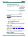
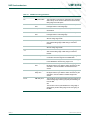
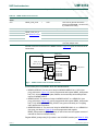
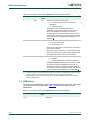
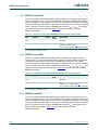
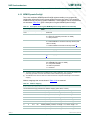
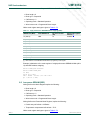
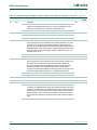
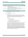
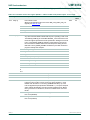
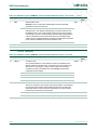
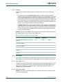
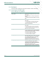
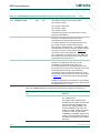
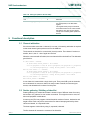
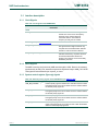
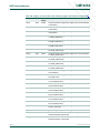
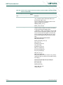
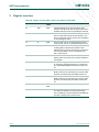
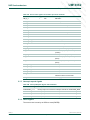
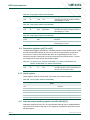
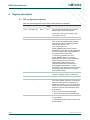
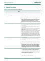
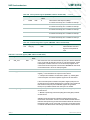
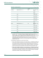
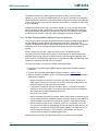
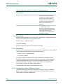
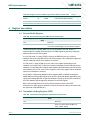
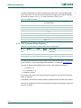
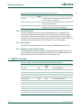
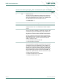
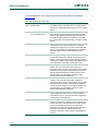
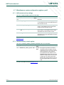
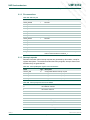
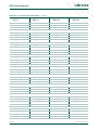
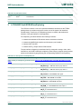
Symbol
Access Reset
Value
Description
31:1
-
-
-
Reserved
0
nhp_mode R/W
0
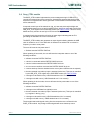
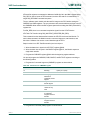
NHP mode bit. Setting this bit puts the SPI in ’NHP mode’
and protects the receive FIFO contents from speculative
reads. Now a read of the FIFO_DATA register only returns
the data from the FIFO, but will not result in updating of the
FIFO's read pointer as a side effect. Speculative reads of
the FIFO_DATA register will not cause data loss of the
received FIFO. After every read of data, the NHP pop
register needs to be written, in order to remove the read
element from the FIFO, and to point to the next element.
FT
FT
A
A
R
R
D
D
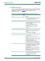
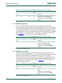
Bit
F
FT
FT
A
A
R
R
D
D
D
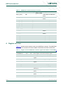
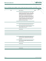
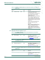
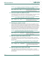
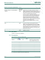
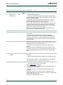
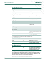
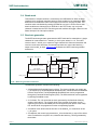
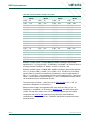
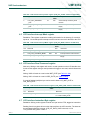
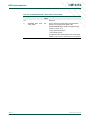
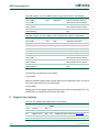
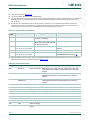
Table 395. NHP mode register (NHP_MODE, address 0x1500 2014)
FT
UM10362
FT
FT
NXP Semiconductors
D
D
R
A
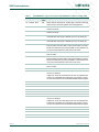
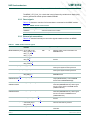
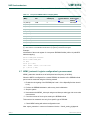
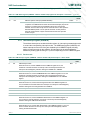
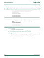
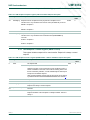
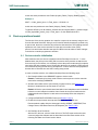
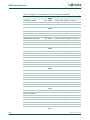
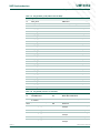
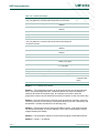
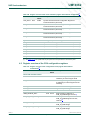
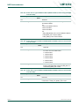
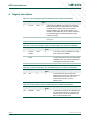
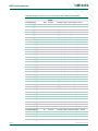
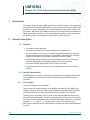
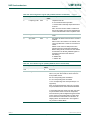
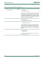
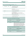
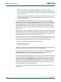
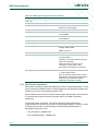
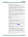
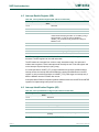
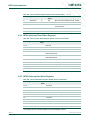
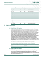
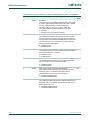
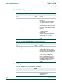
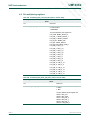
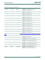
Access
Reset
Value
Description
31:8
-
-
0x0
Reserved.
7:5
-
-
0x0
Reserved.
4:2
-
-
0x0
Reserved.
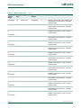
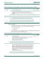
1
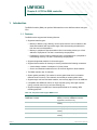
tx_dma_enable
R/W
0
Tx DMA enable bit 1: DMA enabled 0: DMA
disabled
0
rx_dma_enable
R/W
0
Rx DMA enable bit 1: DMA enabled 0: DMA
disabled.
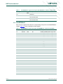
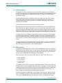
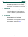
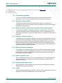
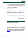
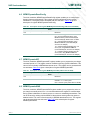
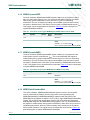
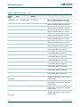
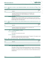
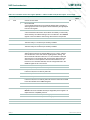
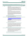
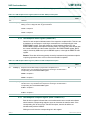
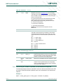
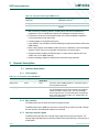
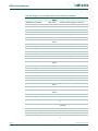
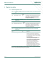
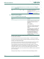
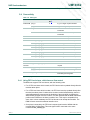
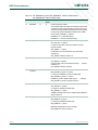
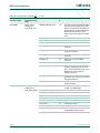
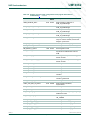
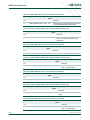
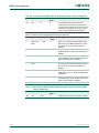
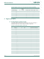
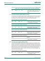
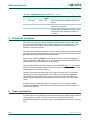
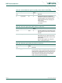
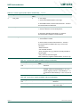
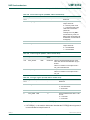
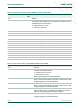
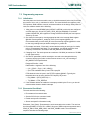
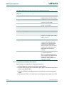
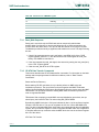
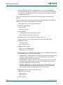
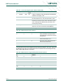
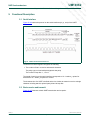
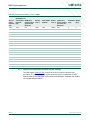
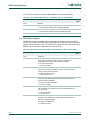
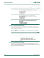
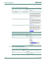
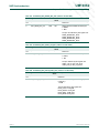
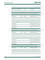
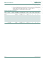
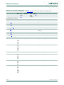
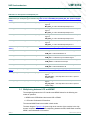
Table 397. Status register (STATUS, address 0x1500 201C)
Bit
Symbol
Access
Reset
Value
Description
31:6
-
-
0
Reserved.
5
Sms_mode_busy R
0
Sequential multi-slave mode busy flag
1: SPI is currently transmitting in sequential
multi-slave mode, once all data to all slaves has
been sent, this bit is cleared
0: SPI is not in sequential multi-slave mode or not
busy transmitting in this mode.
4
spi_busy
R
0
SPI busy flag
1: SPI is currently transmitting and/or receiving or
the transmit FIFO is not empty 0: SPI is idle.
3
rx_fifo_full
R
0
Receive FIFO full bit
1: receive FIFO full 0: receive FIFO not full.
UM10362_0
User manual
© NXP B.V. 2009. All rights reserved.
Rev. 00.02 — 9 September 2009
361 of 577
A
Symbol
R
Bit
D
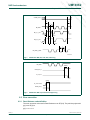
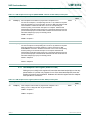
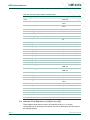
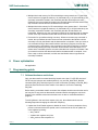
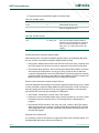
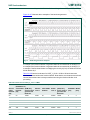
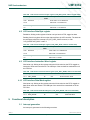
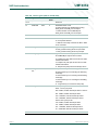
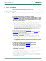
Table 396. DMA setting register (DMA_SETTINGS, address 0x1500 2018)
FT
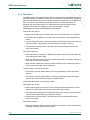
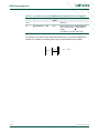
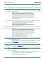
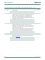
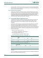
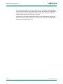
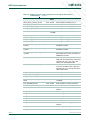
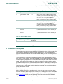
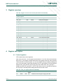
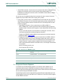
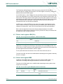
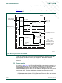
Clearing the bit disables the NHP mode. An explicit pop of
the receive FIFO is no longer needed. Reading the
FIFO_DATA register also updates the receive FIFO's read
pointer as a side-effect.