1
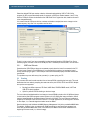
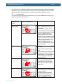
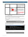
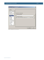
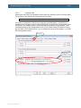
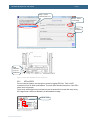
LPC3131/41 Developer’s Kit - User’s Guide Copyright 2012 © Embedded Artists AB LPC3131/41 Developer’s Kit User’s Guide Get Up-and-Running Quickly and Start Developing Your Applications On Day 1! EA2-USG-0901 Rev K LPC3131/41 Developer’s Kit - User’s Guide Page 2 Embedded Artists AB Davidshallsgatan 16 SE-211 45 Malmö Sweden [email protected] http://www.EmbeddedArtists.com Copyright 2005-2012 © Embedded Artists AB. All rights reserved. No part of this publication may be reproduced, transmitted, transcribed, stored in a retrieval system, or translated into any language or computer language, in any form or by any means, electronic, mechanical, magnetic, optical, chemical, manual or otherwise, without the prior written permission of Embedded Artists AB. Disclaimer Embedded Artists AB makes no representation or warranties with respect to the contents hereof and specifically disclaim any implied warranties or merchantability or fitness for any particular purpose. Information in this publication is subject to change without notice and does not represent a commitment on the part of Embedded Artists AB. Feedback We appreciate any feedback you may have for improvements on this document. Please send your comments to [email protected]. Trademarks All brand and product names mentioned herein are trademarks, services marks, registered trademarks, or registered service marks of their respective owners and should be treated as such. Copyright 2012 © Embedded Artists AB LPC3131/41 Developer’s Kit - User’s Guide Page 3 Table of Contents 1 Document Revision History 5 2 Introduction 6 2.1 Features 6 2.2 ESD and Handling Precaution 7 2.3 LPC3131/41 Core Voltage Precaution 7 2.4 CE Assessment 8 2.5 Other Products from Embedded Artists 8 2.5.1 Design and Production Services 8 2.5.2 OEM / Education / QuickStart Boards and Kits 8 3 LPC3131/41 OEM Board Design 3.1.1 Page 2: Powering 3.1.2 Page 3: LPC3131/41 CPU 10 3.1.3 Page 4: External Memories 11 3.1.4 Page 5: Expansion Connector 12 9 3.2 Usage of CPU Pins 12 3.3 LPC3131/41 OEM Board Mechanical Dimensions and Connector 15 3.4 Things to note about the LPC3131/41 OEM Board 15 3.4.1 NAND FLASH Bad Block 15 3.4.2 Brand of Memory Chips 15 4 LPC31xx Base Board Design 16 4.1 Usage of CPU Pins 16 4.2 Known Limitation / Things to note about the LPC31xx Base Board 18 4.2.1 Codec Usage and Boot Mode 18 4.2.2 NAND Booting 18 4.2.3 SD/MMC card detect 19 4.2.4 USB Host applications – power supply 19 4.2.5 USB Host applications – over current sense 19 4.3 Jumpers 20 4.3.1 Default Jumper Positions 21 4.3.2 Illegal Jumper Combinations 21 4.4 Connectors 22 4.5 Important Components 23 4.6 NAND Boot Problem Fix 24 5 Getting Started 26 5.1 Initial Setup and Powering 26 5.2 FTDI USB Driver 26 5.2.1 5.3 Copyright 2012 © Embedded Artists AB 9 USB Driver Behavior Booting 29 29 5.3.1 Jumper Settings 30 5.3.2 Creating a Boot Image 31 LPC3131/41 Developer’s Kit - User’s Guide Copyright 2012 © Embedded Artists AB Page 4 5.3.3 Booting via UART 35 5.3.4 Booting via SPI NOR flash 35 5.3.5 Booting via USB DFU class 36 5.3.6 LED on GPIO2 37 5.3.7 Booting via NAND Flash 38 6 Further Information 39 LPC3131/41 Developer’s Kit - User’s Guide Page 5 1 Document Revision History Revision Date Description A 2009-03-09 First complete version. Add description about booting and correct language and spelling errors. B 2009-04-11 Update description of MMC/SD card detect fix and codec handling. C 2009-05-05 Update description for LPC31xx Base Board v2.0 (with Ethernet). D 2009-06-18 Update with description for EWARM. E 2009-09-09 Added information about LPC3141. Added information about NAND boot and LCD/Ethernet problem (section 5.3.6). F 2009-11-27 Changed title of manual to ‘Developer’s Kit” manual. Updated OEM Board schematic to v1.2. Replaced earlier section 5.3.6 with new section about NAND boot and LCD/Ethernet problem (section 4.6 ). G 2010-07-05 Added information in section 4.2 about things to note about the LPC31xx Base Board (UDA1380 I2C address, SD card detect logic, USB Host powering). H 2010-11-15 Updated information about NAND boot problem. I 2011-08-24 Added information about VBUS over-current sense for USB Host applications (section 4.2.5 ). J 2011-12-19 Added note about CE marking. Removed schematics from document. K Copyright 2012 © Embedded Artists AB 2012-05-10 Updated section 5.3.4 about SPI NOR boot. Added section 5.3.7 about booting from NAND flash. LPC3131/41 Developer’s Kit - User’s Guide Page 6 2 Introduction Thank you for buying Embedded Artists’ LPC3131/41 Developer’s Kit based on NXP’s ARM926EJ-S LPC3131/41 microcontroller. This document is a User’s Guide that describes the LPC3131/41 OEM Board and the LPC31xx Base Board hardware design. It is the User’s Manual for both the LPC3131/41Developer’s Kit as well as for just the LPC3131/41 OEM Board. 2.1 Features Embedded Artists’ LPC3131/41 Developer’s Kit with NXP’s ARM926EJ-S LPC3131/41 microcontroller lets you get up-and-running quickly. The small sized OEM board offers many unique features that ease your learning curve and speed up your program development. The board has also been designed for OEM applications with volume discount available. The features of the LPC3131/41 OEM board are: NXP's ARM926EJ-S LPC3131/41 microcontroller in BGA package, with 192 KByte internal RAM External data memory: 64 MB SDRAM (16-bit databus width) External FLASH memories: 256 MB (2Gbit) NAND FLASH and 4 MB (32Mbit) SPI-NOR FLASH 12.0000 MHz crystal for maximum execution speed and standard serial bit rates, including CAN and USB requirements 256 Kbit I2C E2PROM for storing non-volatile parameters Buffered 16-bit data bus for external expansion 200 pos expansion connector (SODIMM-200 format, 0.6mm pitch) All LPC3131/41 pins available (except dedicated pins for on-board memories) +5V only powering Onboard reset generation Compact SODIMM size: 66 x 48 mm Six layer PCB design for best noise immunity There is an accompanying LPC31xx Base Board that can be used for initial prototyping work. The features of the board are: Copyright 2012 © Embedded Artists AB Connectors 200 pos, 0.6mm pitch SODIMM connector for LPC3131/41 OEM Board RJ45 Ethernet connector (available on base board from v2.0) Expansion connector to 3.2 inch QVGA TFT color LCD with touch panel Three expansion connectors with all SODIMM signals MMC/SD interface and connector USB OTG or Host connectors Four 3.5mm audio connectors (mic in, line in, line out, headphone out) JTAG connector 2.1mm power input LPC3131/41 Developer’s Kit - User’s Guide Power 2.2 Page 7 Power supply, either via USB or external 9-15V DC (LPC3131/41 OEM Board is powered with +5V) Current monitors on input voltages Other 100/10Mbps Ethernet interface base on DM9000A chip (available on base board from v2.0) UDA1380 I2S codec with mic in, line in, line out, and headphone out 5-key joystick (via I2C) 3-axis accelerometer 8 LEDs (via I2C) Trimpot analog input USB-to-serial bridge on UART (FT232R) RS232 alternative interface on UART XBee™ RF-module alternative interface on UART (note that XBee module is not included in bundle) Reset push-button and LED 205x135 mm in size ESD and Handling Precaution Please note that the LPC3131/41 OEM Board and LPC31xx Base Board come without any case/box and all components are exposed for finger touches – and therefore extra attention must be paid to ESD (Electro-Static Discharge) precaution. Make it a habit to always first touch the metal surface of one of the USB or SC/MMC connectors for a few seconds with both hands before touching any other parts of the boards. That way, you will have the same electrical potential as the board and therefore minimize the risk for ESD. Never touch directly on the LPC3131/41 OEM Board and in general as little as possible on the LPC31xx Base Board. The keys on the LPC31xx Base Board have grounded shields to minimize the effect of ESD. Note that Embedded Artists does not replace boards that have been damaged by ESD. In case you have also connected the QVGA Display Module to the LPC31xx Base Board, do not exercise excessive pressure on the LCD glass area. That will damage the display. Also, do not apply pressure on the two flex cables connecting the LCD. These are relatively sensitive and can be damaged if too much pressure is applied to them. Note that Embedded Artists do not replace QVGA Display Modules where the LCD has been improperly handled. 2.3 LPC3131/41 Core Voltage Precaution The core voltage for the LPC3131/41 can be dynamically changed, via I2C commands sent to the LTC3447 voltage converter. The voltage can be set to up to 2V. Note that this is above the limits of the core voltage. See LPC3131/41 datasheet for details (the maximum core voltage is 1.30V). Copyright 2012 © Embedded Artists AB LPC3131/41 Developer’s Kit - User’s Guide Page 8 Note that Embedded Artists do not replace LPC3131/41 OEM boards where the core voltage (VDD(CORE)) has been raised above 1.30 Volt. It is the user’s responsibility not to exceed the voltage specification found in the datasheet. On version 1.1 boards, two zero ohm resistors/jumpers must be soldered to the LPC3131/41 OEM Board in order to connect the I2C communication channel of the LTC3447 to I2C channel#1. See the schematic for details. 2.4 CE Assessment The LPC3131/41 Developers Kit (consisting of the LPC3131/41 OEM Board and LPC31xx Base Board) is CE marked. See separate CE Declaration of Conformity document. The LPC3131/41 Developers Kit is a class A product. In a domestic environment this product may cause radio interference in which case the user may be required to take adequate measures. EMC emission test has been performed on the LPC3131/41 Developers Kit. Standard interfaces like Ethernet, USB, serial have been in use. General expansion connectors where internal signals are made available (for example processor pins) have been left unconnected. Connecting other devices to the product via the general expansion connectors may alter EMC emission. It is the user’s responsibility to make sure EMC emission limits are not exceeded when connecting other devices to the general expansion connectors of the LPC3131/41 Developers Kit. Due to the nature of the LPC3131/41 Developers Kit – an evaluation board not for integration into an end-product – fast transient immunity tests and conducted radio-frequency immunity tests have not been executed. Externally connected cables are assumed to be less than 3 meters. The general expansion connectors where internal signals are made available do not have any other ESD protection than from the chip themselves. Observe ESD precaution. Note that the LPC3131/41 OEM board is classified as a component and is hence not CE marked separately. It can perform different functions in different integrations and it does not have a direct function. It is therefore not in the scope of the CE Directive. An end product, where an OEM Board is integration into, is however very likely to need CE marking. 2.5 Other Products from Embedded Artists Embedded Artists have a broad range of LPC1xxx/LPC2xxx/LPC3xxx/LPC4xxx based boards that are very low cost and developed for prototyping / development as well as for OEM applications. Modifications for OEM applications can be done easily, even for modest production volumes. Contact Embedded Artists for further information about design and production services. 2.5.1 Design and Production Services Embedded Artists provide design services for custom designs, either completely new or modification to existing boards. Specific peripherals and I/O can be added easily to different designs, for example, communication interfaces, specific analog or digital I/O, and power supplies. Embedded Artists has a broad, and long, experience in designing industrial electronics in general and with NXP’s LPC2xxx microcontroller family in specific. Our competence also includes wireless and wired communication for embedded systems. For example IEEE802.11b/g (WLAN), Bluetooth™, ZigBee™, ISM RF, Ethernet, CAN, RS485, and Fieldbuses. 2.5.2 OEM / Education / QuickStart Boards and Kits Visit Embedded Artists’ home page, www.EmbeddedArtists.com, for information about other OEM / Education / QuickStart boards / kits or contact your local distributor. Copyright 2012 © Embedded Artists AB LPC3131/41 Developer’s Kit - User’s Guide Page 9 3 LPC3131/41 OEM Board Design This chapter contains detailed information about the electrical and mechanical design of the LPC3131/41 OEM Board. Note that it is version 1.2 of the board that is presented. Differences from version 1.1 and 1.0 are small and can be seen in the schematic (first page). The schematic can be downloaded in pdf format from the support page, and is recommended to have printed out while reading this chapter. The following subsections describe in more detail each part of the design. 3.1.1 Page 2: Powering Page 2 of the schematic contains the power supplies of the LPC3131/41 OEM Board. 3.1.1.1 1.8V and 3.3V Voltages The LPC3131/41 requires three voltages; 1.2V for the core, 1.8V for the memory interface and 3.3V for the rest of the i/o interfaces. The 1.8V and 3.3V voltages are fixed and generated by two LM3671MF step-down switching regulators from National Semiconductor. These regulators are capable of generating 600mA, which by far exceed the needed current by the LPC3131/41 and other components on the LPC3131/41 OEM Board. 3.1.1.2 1.2V Adjustable Core Voltage The core 1.2V voltage is adjustable and is generated by the step down switching regulator LTC3447 from Linear Technologies. This regulator is capable of generating 600mA, which also by far exceed the needed current by the LPC3131/41. The adjustment is done via an I2C channel, I2C1 in the LPC3131/41 case. The core voltage can be adjusted as a power save feature. By lowering the voltage, the total power consumption can be lowered but the clock frequency of the core must then also be lowered. This is a trade-off that is important for hand held equipment. Note that it is the user’s responsibility not to program the LTC3447 to generate too high core voltage, which is possible. The LTC3447 can generate voltages up to 2V, which by far exceed the limits for the LPC3131/41. To minimize the risk of accidentally setting the voltage the I2C channel is disconnected via R56/R57 (which are 0 ohm resistors/jumpers that are not mounted). R56/R57 is the only thing that differs between v1.0 and v1.1 of the board. On v1.0, the I2C1 of the LPC3131/41 is always connected to the LTC3447. See the LPC3131/41 datasheet for exact details about ranges, but it is in the region of 1.1-1.3V. Also see the LTC3447 datasheet for details about how to adjust the voltage (it is a write-only register). The I2C address for the LTC3447 is indicated in the schematic. 3.1.1.3 Input Voltage The input voltage to the LPC3131/41 OEM Board is given by the requirements of the LM3671 and LTC3447. A recommended input voltage range is 3.4 – 5.5V. The input supply must be stable but there are no special needs for bulk capacitors close to the power pins on the expansion connectors. The needed capacitors are placed close to the step down switching regulators on the LPC3131/41 OEM Board. 3.1.1.4 OTP VPP Voltage The VPP power to the LPC3131 is fixed to 1.2V. The LPC3141 has on-chip OTP (One-Time Programmable) fuses that can be programmed. 3.3V must be applied to VPP during programming. The OTP voltage switch (U4) is mounted on LPC3141 OEM Boards, but not on LPC3131 OEM Boards. Copyright 2012 © Embedded Artists AB LPC3131/41 Developer’s Kit - User’s Guide 3.1.2 Page 10 Page 3: LPC3131/41 CPU Page 3 of the schematic contains the core part of the design, which of course is the LPC3131/41 microcontroller. It is an ARM926EJ-S cpu core with a lot of different peripheral units and on-chip memory (192 KByte SRAM). 3.1.2.1 12MHx Crystal and PLLs The microcontroller crystal frequency is 12.0000 MHz. This frequency is the recommended from NXP. There is dual on-chip PLLs on the LPC3131/41 in order to generate different needed frequencies for the chip. Note that the clocking structure is very different from the LPC2xxx family. It is a more complex structure but also much more versatile and flexible. There is no shortcut but to read the LPC3131/41 User’s Manual in detail and understand the options and settings. The main thing differing between the LPC3131 and the LPC3141 is the maximum core frequency for the processor. See datasheet for details. 3.1.2.2 Booting The LPC3131/41 starts executing from an on-chip ROM, containing the bootloader. Note that the LPC3131/41 does not contain any on-chip FLASH memory. Program code must be loaded from an external source into the on-chip SRAM. There are multiple boot options, as indicated in the schematic. The default is set to UART mode booting. Normally the default boot option can be controlled/changed from the LPC31xx Base Board, but the default resistors can also be changed for special orders of the board. The LPC3131/41 OEM Board contains both SPI NOR flash and NAND flash in order to support stand alone booting. Section 4.6 contains important information if NAND boot is used. 3.1.2.3 JTAG interface The JTAG interface is a standard ARM-compatible JTAG interface. There is a special feature on the LPC3131/41 that can bypass the ARM core scan chain (i.e. the debug access), by pulling JTAGSEL low. In that case, the JTAG interface is used for boundary scan access. The multiplexer (U17) selects the different scan chain outputs depending on the JTAGSEL signal. Normally this has no affect on the operation since the input signal JTAG_DBGEN (connected to JTAGSEL) is held high. 3.1.2.4 SPI NOR FLASH There is a 32Mbit (4 MByte) NOR flash connected to the SPI bus. There is an option to mount one of two different manufacturers; either S25FL032 from Spansion or AT45DB321 from Atmel. Embedded Artists can choose to mount any one of these chips (or similar) on the board and it depends on component availability at the time of production. Both are compatible for the relevant commands. In case special commands are used, it is possible to read out chip id and determine type. 3.1.2.5 Reset Generation The reset generation is handled by a standard voltage supervisor chip, CAT811R from Catalyst Semiconductor. The reset signal will be held active (i.e., low) until the supply voltages, +3.3V, is within margins (above 2.63V). The reset duration is typically 200 mS (consult the CAT811R datasheet for exact details). The output reset signal is push/pull output that is converted to an open-collector / opendrain output via the 74LVC1G125 buffer. An external reset source can pull the reset signal low (with an open-collector/open-drain output). 3.1.2.6 I2C E2PROM There is a 256 kbit E2PROM accessible via the I2C interface. The LPC3131/41 has two on-chip I2C communication channels. Channel #0 is used for communicating with the E2PROM. More peripheral units are easily connected to the two-wire I2C bus, just as long as the addresses do not collide. The address of the 256kbit E2PROM is 0xA0, which is also indicated in the schematic. Copyright 2012 © Embedded Artists AB LPC3131/41 Developer’s Kit - User’s Guide Page 11 There are 1.5 kohm pull-up resistors (pull-ups are always needed on I2C busses) included on the board on I2C channel #0. 3.1.2.7 USB Interface There is a high-speed USB 2.0 (OTG, Host, Device) interface with on-chip PHY on the LPC3131/41. Note that special care must be taken for layout of the USB signals. This also applies for the external connector, connected to the expansion interface of the LPC3131/41 OEM Board. 3.1.2.8 Analog Inputs The LPC3131/41 contains a 10-bit ADC (Analog to Digital Converter). The positive reference voltage is ADC_VREFP (found on page 2 of the schematic). It is a filtered version of the 3.3V voltage. The voltage ADC_VREFP is available on the expansion connector. There is also an associated analog ground reference available on the expansion connector (connected to pin ADC10B_GND on the LPC3131/41). 3.1.3 Page 4: External Memories Page 4 of the schematic contains the external memory interface and the external memories. There are two memory components connected to the external 16-bit memory bus interface. Note that the LCD interface and external memory bus interface are multiplexed over the same pins. It is the memory bus interface that is used in the LPC3131/41 OEM Board. The LCD interface cannot be used and shall not be enabled in the cpu. Also note that three different types of memories share the same bus interface: Dynamic memories (SDRAM) Using signals RAS/CAS/DQM0/DQM1/ CLOCKOUT/CKE, etc. Static memories or general peripherals Using signals OE/WE/BLOUT0/BLOUT1, etc. NAND Flash memories Using signals CLE/ALE, etc. Many of the signals are multiplexed on the same pins. The memory interface operates at 1.8V level, which minimizes power consumption. 3.1.3.1 Memory Layout The external memory controller on the LPC3131/41 defines a number of memory regions, as listed below: External SDRAM bank 0 (0x3000 0000 – 0x33FF FFFF) 16-bit databus width and 64MByte in size. External SRAM bank 0 (0x2000 0000 – 0x2000 FFFF / 0x2001 FFFF) 128 kByte in size for 16-bit databus width and 64 kByte in size for 8-bit databus. External SRAM bank 1 (0x2002 0000 – 0x2002 FFFF / 0x2003 FFFF) 128 kByte in size for 16-bit databus width and 64 kByte in size for 8-bit databus. NAND band 0-3 (accessible via NAND flash controller, not directly via memory address) The LPC3131/41 OEM Board uses the external SDRAM bank 0 as well as NAND bank 0. It is mainly the two external SRAM banks that are available for the off-board external memory interface of the LPC3131/41 OEM Board. Chip select signals N_STCS0 and N_STCS1 are free for external use via the buffered memory interface. Both the address and the data busses are buffered. Copyright 2012 © Embedded Artists AB LPC3131/41 Developer’s Kit - User’s Guide Page 12 3.1.3.2 SDRAM A 512 MBit (64 MByte) Mobile SDRAM is used, MT48H32M16LF from Micron. The chip is powered by 1.8V and is organized as 32Mbitx16, i.e. it has 16-bit databus width. The chip occupies the only available memory bank for dynamic RAM at address range 0x3000 0000 – 0x33FF FFFF. 3.1.3.3 NAND Flash A 2 Gbit (256) NAND flash is used, MT29F2G08ABDHC from Micron. The chip is powered by 1.8V and has 8-bit databus width. The NAND flash builds on a single-level cell (SLC) technology and has a page size of 2112 bytes (2,048 + 64 bytes). The chip is connected to NAND bank 0. Note that the chip is not directly accessible via the memory bus. Instead, all accesses must be done via the on-chip NAND flash controller of the LPC3131/41. Embedded Artists can choose to mount a different brand of NAND flash dependent on component availability at the time of production. The application program should always read out the NAND flash chip id and determine type and features. 3.1.3.4 Buffers to External Interface The LPC3131/41 memory interface is available on the expansion connector. The data bus width is 16bits on the external interface. The relevant signals are buffered. The buffers are disabled by default unless enabled by external signals. By pulling signal N_ABUF_EN low, the two buffers for address and control signals are enabled and act as outputs (from the LPC3131/41 OEM Board). The data bus buffer is controlled by the signal N_DBUF_EN. By pulling this signal low, the data bus buffer is enabled. The buffered version of the LPC3131/41 signal OE controls the direction of the data bus buffer. During read operations the buffer acts as an input and during write operations it acts as an output. Note that N_DBUF_EN must not be pulled low constantly. In that case the buffer will collide with the board’s internal data bus. N_DBUF_EN must only be pulled low when an external memory/IO device is accessed. If only one of the static chip selects is used externally, just connect that signal to N_DBUF_EN. If more than one chip select signal is used, (logically) AND all chip select signal together before driving the N_DBUF_EN signal, in this case, just AND the two signals B_N_STCS0 and B_N_STCS1. There is an additional important note when booting from NAND flash, read section 4.6 for details about the N_DBUF_EN signal. If the external memory interface is not used, leave ABUS_EN and DBUS_EN unconnected. The buffers are dual voltage buffers and act as level translators between the internal 1.8V signal levels and the external levels. Connect the external bus voltage to VDD_EXT. See the datasheet of 74AVCA164245 for exact details about voltage range. Normally 3.3V powering is used. 3.1.4 Page 5: Expansion Connector The LPC3131/41 OEM Board integrates the core part of a typical LPC3131/41 board design with a reasonable large amount of external memories. All relevant signals of LPC3131/41 are available on the 200 pos, 0.6mm pitch expansion connector (SODIMM-200 format). See next section for a detailed list of available pins. 3.2 Usage of CPU Pins Almost all pins of the LPC3131/41 are directly available on the expansion connectors. Only in a few cases pins are used for dedicated functionality like (dynamic) memory control signals and chip select signals. Such pins are not available on the expansion connector. The table below lists all pins and their possible restrictions. Copyright 2012 © Embedded Artists AB LPC3131 OEM Board - User’s Guide Copyright 2009 © Embedded Artists AB Pin Available on expansion connector USB_VBUS USB_DM USB_DP USB_ID Yes I2C_SDA0 I2C_SCL0 Yes, but I2C E2PROM connected to these pins. I2C_SDA1 I2C_SCL1 Yes, but LTC3447 is connected to these pins on v1.0 boards. Can be connected on v1.1 boards. SPI_CS_OUT0 No, signal used for chip select of SPI NOR flash (U7 or U10). SPI_SCK SPI_MISO SPI_MOSI SPI_CS_IN Yes, but note that SPI NOR flash is connected to SPI_SCK, SPI_MISO, SPI_MOSI. UART_RXD UART_TXD UART_CTS/SPI_CS_OUT1 UART_RTS/SPI_CS_OUT2 Yes I2SRX_DATA0 I2SRX_WS0 I2SRX_BCK0 I2STX_DATA0 I2STX_WS0 I2STX_BCK0 Yes I2SRX_DATA1 I2SRX_WS1 I2SRX_BCK1 I2STX_DATA1 I2STX_WS1 I2STX_BCK1 Yes GPIO0 GPIO1 GPIO2 Yes, but pull-ups/pull-downs are used to set default boot mode to booting from the UART. GPIO3-GPIO20 Yes PWM_DATA Yes ADC10B_GPA0-ADC10B_GPA3 Yes CLK_256FS_O CLOCK_OUT Yes EA2-USG-0901 v0.1 Rev A LPC3131/41 Developer’s Kit - User’s Guide Page 14 SYSCLK_O EBI_D0-EBI_D15 Yes, but only available via the data bus buffer MLCD_A0/ALE MLCD_A1/CLK MLCD_DB2/EBI_A2 MLCD_DB3/EBI_A3 MLCD_DB4/EBI_A4 MLCD_DB5/EBI_A5 MLCD_DB6/EBI_A6 MLCD_DB7/EBI_A7 MLCD_DB8/EBI_A8 MLCD_DB9/EBI_A9 MLCD_DB10/EBI_A10 MLCD_DB11/EBI_A11 MLCD_DB12/EBI_A12 MLCD_DB13/EBI_A13 MLCD_DB14/EBI_A14 MLCD_DB15/EBI_A15 Yes, but only available via the address bus buffer EBI_DQM0/NOE EBI_NWE EBI_NCAS/BLOUT0 EBI_NRAS/BLOUT1 MLCD_CSB/EBI_NSTCS0 MLCD_DB1/EBI_NSTCS1 Yes, but only available via the buffer NAND_NCS0 MNAND_RYBN0/MCI_DATA4 No, used for internal NAND flash memory. NAND_NCS1 NAND_NCS2 NAND_NCS3 MNAND_RYBN1/MCI_DATA5 MNAND_RYBN2/MCI_DATA6 MNAND_RYBN3/MCI_DATA7 Yes MLCD_DB0/EBI_CLKOUT MLCD_RS/EBI_NDYCS MLCD_RW_WR/EBI_DQM1 MLCD_E_RD/EBI_CKE No, used for internal SDRAM. ADC_REFP ADC_REFN Yes. Note that VDDA is connected to +3.3V power supply FFAST_IN FFAST_OUT No, directly connected to on-board crystals JTAG signals Yes, except for BUF_TRTS_N, BUF_TCK, BUF_TMS RESET_IN Yes Copyright 2011 © Embedded Artists AB LPC3131/41 Developer’s Kit - User’s Guide Page 15 The LPC31xx Base Board illustrates how to typically connect external interfaces (like USB, external memory devices, etc) to the LPC3131/41 OEM Board. Study this schematic for details. 3.3 LPC3131/41 OEM Board Mechanical Dimensions and Connector Figure 1 below contains a drawing of the board that includes mechanical measures. See SODIMM-200 standard for exact measures. 1.8V keying is used (SODIMM-200 boards are either 1.8V or 2.5V keyed). 66 mm 48 mm 1.8V keying of SODIMM board Figure 1 – LPC3131/41 OEM Board Mechanical Dimensions The SODIMM-200 format is a standard and there exist many connectors that are suitable from many different manufactures. The many sources also keep the connector cost very low. Note that the connector should be 1.8V keyed. See document OEM Board Integration Guide for more information about suitable connectors, but basically any SODIMM, DDR2, 200pos, 1.8V, right-angled connector will do. 3.4 Things to note about the LPC3131/41 OEM Board 3.4.1 NAND FLASH Bad Block The NAND Flash is the MT29F2G08ABDHC from Micron and contains 2 GBit capacity. The chip may include invalid blocks when shipped from factory. A maximum of 40 invalid blocks may exist initially, i.e., 2008-2048 valid blocks. Additional invalid blocks may develop while being used. Invalid blocks are defined as blocks that contain one or more bad bits. Do not erase or program factory-marked bad blocks. More information about appropriate management of invalid blocks can be found in technical notes and datasheet from Micron. 3.4.2 Brand of Memory Chips Note that there is no guarantee for a certain brand or version of memory chips; SPI-NOR flash, parallel NAND flash and SDRAM. The lifetime of memory chips is limited and availability can also be limited from time to time. Embedded Artists make every effort to mount the original design chip on the board. In case that is impossible a compatible chip will instead be mounted without any prior notice. There can be small programming differences between mounted brands. The application program shall always read the chip id of flash devices to make certain which chip is actually mounted on the board. The support page contains datasheets to the different memory devices and information about mounted devices on different board versions. Copyright 2011 © Embedded Artists AB LPC3131/41 Developer’s Kit - User’s Guide Page 16 4 LPC31xx Base Board Design This chapter contains detailed information about the electrical and mechanical design of the LPC31xx Base Board, version 2.0. The difference between v1.1 and v2.0 is that a 100/10Mbps Ethernet interface was added in v2.0. This new functionality is found on page 8 of the schematic. The differences between version 1.0 and v1.1 are very small and can be seen on revision comments on the first page of the schematic. The schematic can be downloaded in pdf format from the support page, and is recommended to have printed out while reading this chapter. The LPC31xx Base Board contains a number of interfaces and connectors to the LPC3131/41 OEM Board. The design can be viewed as a reference schematic for custom designs around the LPC3131/41 OEM Board. Note that there is some future functionality on the LPC31xx Base Board, which does not directly apply for the LPC3131/41 OEM Board. 4.1 Usage of CPU Pins Almost all pins of the LPC3131/41 are directly available on the expansion connectors. Only in a few cases are pins used for dedicated functionality like (dynamic) memory control signals and chip select signals. Such pins are not available on the expansion connector. The table below lists all pins and their possible restrictions. Pin Usage on LPC31xx Base Board USB_VBUS USB_DM USB_DP USB_ID Connected to USB connectors; mini-AB and A. I2C_SDA0 I2C_SCL0 Connected to PCA9532 port expander. I2C_SDA1 I2C_SCL1 Connected to UDA1380 codec for controlling the codec. SPI_SCK SPI_MISO SPI_MOSI Can be connected to QVGA display for touch screen controller SPI interface. SPI_CS_IN No usage. UART_RXD UART_TXD Can be connected to the USB-to-serial bridge, RS232 interface or XBee module. UART_CTS/SPI_CS_OUT1 Can be connected to QVGA display for touch screen controller SPI interface (chip select). Can be connected to RS232 interface or XBee module. UART_RTS/SPI_CS_OUT2 Can be connected to RS232 interface or XBee module. I2SRX_DATA0 Can be used to detect presence of +5V. I2SRX_WS0 Can be used to detect USB power switch over-current status I2SRX_BCK0 No usage. Copyright 2011 © Embedded Artists AB LPC3131/41 Developer’s Kit - User’s Guide Page 17 I2STX_WS0 I2STX_DATA0 Can be used to control powering of MMC/SD memory card interface. I2STX_BCK0 Can be used to detect MMC/SD memory card presence. I2SRX_DATA1 I2SRX_WS1 I2SRX_BCK1 I2STX_DATA1 I2STX_WS1 I2STX_BCK1 Can be connected to UDA1380 codec. GPIO0 GPIO1 GPIO2 Can be connected to jumpers for controlling boot mode. GPIO3 No usage. GPIO4 Can be used as QVGA display touch screen controller interrupt pin. GPIO5 Can be used as MCI_CLK (MMC/SD interface) GPIO6 Can be used as MCI_CMD (MMC/SD interface) GPIO7 Can be used as MCI_DAT0 (MMC/SD interface) GPIO8 Can be used as MCI_DAT1 (MMC/SD interface) GPIO9 Can be used as MCI_DAT2 (MMC/SD interface) GPIO10 Can be used as MCI_DAT3 (MMC/SD interface) GPIO11-GPIO20 No usage. PWM_DATA Can be used to control backlight intensity on QVGA display ADC10B_GPA0 X-output from accelerometer. ADC10B_GPA1 Y-output from accelerometer. ADC10B_GPA2 Either z-output from accelerometer or trim pot. ADC10B_GPA3 No usage. CLK_256FS_O 256 Fs clock to UDA1380 codec. CLOCK_OUT SYSCLK_O No usage. EBI_D0-EBI_D15 Connect to QVGA display module connector and DM9000 Ethernet interface. MLCD_A0/ALE MLCD_A1/CLK MLCD_DB2/EBI_A2 MLCD_DB3/EBI_A3 MLCD_DB4/EBI_A4 MLCD_DB5/EBI_A5 MLCD_DB6/EBI_A6 No usage. Copyright 2011 © Embedded Artists AB LPC3131/41 Developer’s Kit - User’s Guide Page 18 MLCD_DB7/EBI_A7 MLCD_DB8/EBI_A8 MLCD_DB9/EBI_A9 MLCD_DB10/EBI_A10 MLCD_DB11/EBI_A11 MLCD_DB12/EBI_A12 MLCD_DB13/EBI_A13 MLCD_DB14/EBI_A14 MLCD_DB15/EBI_A15 Connect to QVGA display module connector and DM9000 Ethernet interface. EBI_DQM0/NOE EBI_NWE MLCD_CSB/EBI_NSTCS0 Connect to QVGA display module connector and DM9000 Ethernet interface. MLCD_DB1/EBI_NSTCS1 Connect to DM9000 Ethernet interface. EBI_NCAS/BLOUT0 EBI_NRAS/BLOUT1 No usage. NAND_NCS1 NAND_NCS2 NAND_NCS3 MNAND_RYBN1/MCI_DATA5 MNAND_RYBN2/MCI_DATA6 MNAND_RYBN3/MCI_DATA7 No usage. ADC_REFP ADC_REFN Used as references to generate analog signal from trip pot. JTAG signals Connected to standard ARM 2x10 pos JTAG connector. RESET_IN Connected to Reset push-button and LED. 4.2 Known Limitation / Things to note about the LPC31xx Base Board 4.2.1 Codec Usage and Boot Mode The codec, uda1380 (U12), communicate audio data over the I2S bus and command/setting data over the I2C1 bus. Transferring I2S data reliable from the codec to the LPC3131/41 requires booting from JTAG or USB. UART and SPI booting can create an unreliable connection. The problem is under investigation. Transferring I2S data to the codec works. The I2C address of the UDA1380 is also important to understand. The default I2C slave address of LPC313x/4x/5x is the same as the address assigned to UDA1380 on LPC31xx Base Board. Due to this whenever LPC313x/4x/5x as master tries to access UDA1380 the slave logic inside the LPC313x/4x/5x is also reacting causing I2C bus errors. For write this is not a bit problem but for register reads it is. The software running on the LPC313x/4x/5x should change the default I2C slave address before doing any I2C transactions to the UDA1380 on the LPC31xx Base Board. This is done by setting register I2C0_ADR (0x1300A014) & I2C1_ADR (0x1300A414) to 0x6E. The default value for this register is 0x1A (earlier LPC313x User’s Manual has had wrong information about default address, i.e., it is not 0x6E). 4.2.2 NAND Booting Read section 4.6 for details about N_DBUF_EN signal during NAND boot. Copyright 2011 © Embedded Artists AB LPC3131/41 Developer’s Kit - User’s Guide 4.2.3 Page 19 SD/MMC card detect The pull-up on SD card detect pin is after the power switch. Due to this there is a need to enable power to the SD/MMC slot to even detect the card insertion. Note that this problem is fixed on v2.2 of the LPC31xx Base Board. 4.2.4 USB Host applications – power supply When running USB Host applications where the external USB Device draw a considerable amount of current (>100mA), the LPC31xx Base Board must be powered with an external power supply (as opposed to being powered via the USB-to-UART mini-B USB connector). See section 5.1 for details about the external power supply. 4.2.5 USB Host applications – over current sense U3 is an over-current protected distribution switch for VBUS (+5V) – for feeding external USB devices. There is a status flag feedback signal from U3. If this is used (for example by the latest Linux distribution), a jumper must be inserted in J14, pin 9-10. This will bridge the status signal to pin I2SRX_WS0. This jumper is not inserted by default. If the over-current flag on VBUS circuit is not getting set (in case of an over-current situation) it is a sign of too weak external power supply. The problem is typically that when the external load is increasing (on VBUS) the power supply circuit is reducing the output voltage rather than keeping voltage constant and increase the current draw. Due to this the over-current flag is not getting set and eventually the complete board can go “down”, i.e., it resets since the supply voltage is out of range. A possible workaround (if the external power supply cannot keep the voltage at correct level) is to monitor the VBUS voltage to detect an over-current condition and switch VBUS off when it goes below a certain level. Copyright 2012 © Embedded Artists AB LPC3131/41 Developer’s Kit - User’s Guide 4.3 Page 20 Jumpers The LPC31xx Base Board has a number of jumpers in order to be able to connect/disconnect and fully utilize all functionality of the LPC3131/41 and the LPC31xx Base Board. Figure 2 below illustrates all jumpers and explains to what part of the design they belong. Note that v2.0 of the board is shown. V1.0 and v1.1 lack the Ethernet functionality but are equal in all other aspect. USB device connect J22/J21 Connect analog signals to analog inputs Audio jumpers J41, J43/45, J47/49, J50/51/52 Left pos: connect to codec Right pos: connect directly to sodimm board (future functionality) I2S interface J46 Connect I2S channel#1 to codec MMC/SD interface Top J13: enable card detect (note that J13 is removed due to fix on v1.1 boards) Lower J10: select always enabled or controlled UART select J28,J30,J31,J32 Left pos: to RS232 Right pos: to XBee module QVGA interface config From left to right: J36, J33, J35, J34 QVGA interface J39/J38 Connect QVGA display to memory bus and SPI bus (for touch panel) Current monitor J1 Insert to power sodimm board with VBAT (future functionality) Current monitor J3 Insert to power sodimm board with 5V Buffer powering J4 Insert to power buffers on sodimm board with 3.3V USB Host always J16 insert to always force USB Host UOS_VBAT J23 Select source for UOS_VBAT (future functionality) Boot select J20/J19/J18 Left pos: pull high Right pos: pull low Figure 2 – LPC31xx Base Board Jumper Positions Copyright 2012 © Embedded Artists AB Optional Connections J14 ( future functionality) Ethernet enable J55 Enable buffers J40 Insert to enable external memory bus UART select J27/J29 Upper pos: UART to RS232/XBee Lower pos: UART to USB-to-serial bridge LPC3131/41 Developer’s Kit - User’s Guide 4.3.1 Page 21 Default Jumper Positions Figure 3 below illustrates the default jumper positions as mounted when the board is delivered from Embedded Artists. Figure 3 – LPC31xx Base Board Default Jumper Positions 4.3.2 Illegal Jumper Combinations Note that some jumpers are mutual exclusive and should not be inserted simultaneously. Copyright 2012 © Embedded Artists AB Note that the spi chip select on the QVGA display touch controller use the signal UART_CTS_SPI_CS_OUT1. Hence, a jumper between pin 1-2 on J38 should not be inserted while a jumper on J31 is inserted since RTS from the RS232 interface or CTS# from the XBee module will also drive this signal. LPC3131/41 Developer’s Kit - User’s Guide 4.4 Page 22 Connectors Figure 4 below illustrate the position of all external connectors on the LPC31xx Base Board. Mic in J42 Line in 2/ Line out J48 Line in 1 J44 Headphone J52 MMC/SD J12 RS232 DSUB J26 XBee module U10 Power in J24 RJ45Ethernet J56 USB-serial J25 Expansion J6 JTAG J9 USB Host J15 USB OTG J17 Battery connector X2 SODIMM connector X1 Expansion J7 Figure 4 – LPC31xx Base Board External Connectors Copyright 2012 © Embedded Artists AB Expansion J8 QVGA display J37 LPC3131/41 Developer’s Kit - User’s Guide 4.5 Page 23 Important Components Figure 5 below illustrates the position on the LPC31xx Base Board for some important components in the design. Reset push-button and Reset LED Trimming potentiometer for analog input Accelerometer SD/MMC Power LED Voltage measurement pads and Power LED (LED13) USB VBUS LED LED4 Current monitor outputs, J2 & J5 GPIO2-LED LED2 Play-button SW1 Figure 5 – LPC31xx Base Board Important Components Copyright 2012 © Embedded Artists AB LED5-12 USB-to-serial activity LEDs Joystick (SW3) LPC3131/41 Developer’s Kit - User’s Guide 4.6 Page 24 NAND Boot Problem Fix This note does NOT affect boards marked with WO-0246-1033. See picture below where to find production marking. The picture illustrates a board that is not affected. The last four numbers represent a year-week marking. ‘1033’ means produced: 2010, week 33. Boards marked with production dates earlier than 1033 are affected. Production marking Figure 6 – LPC31xx Base Board Production Marking Note that there is a conflict on the databus when booting via NAND flash. The problem is that signals N_STCS0 and N_STCS1 are low during NAND boot. The signal DBUF_EN on the LPC31xx Base Board is formed by AND:ing N_STCS0 and N_STCS1. This, in turn, enables the databus buffer (U16 on LPC3131/41 OEM Board) when the DBUF_EN jumper (pin 1-2 on J40) is inserted on the LPC31xx Base Board. See Figure 7 to locate DBUF_EN jumper on the LPC31xx Base Board. After NAND flash boot is completed the active level changes for the signals N_STCS0 and N_STCS1. Their inactive state is then high and their active state is low, just as expected for memory bus chip select signals. There is unfortunately no way to detect when the NAND boot process is complete. There are however two workarounds for this problem: Copyright 2012 © Embedded Artists AB LPC3131/41 Developer’s Kit - User’s Guide Page 25 1. Remove the DBUF_EN jumper during the boot process and then insert the jumper again in order to use the QVGA and Ethernet functionality on the LPC31xx Base Board. DBUF_EN jumper, pin 1-2 on J40 Figure 7 – DBUF_EN jumper location on LPC31xx Base Board 2. Replace U11 (74LVC1G08), the AND gate found on page 6 of the LPC31xx Base Board schematic. Replace it with a XNOR-gate. The AND and XNOR gates have the same truth table except when both input signals are low. For the XNOR gate the output is high when both inputs are low. This will also solve the problem, since the databus buffer (U16 on LPC3131/41 OEM Board) will not be enabled during NAND boot when both N_STCS0 and N_STCS1 are low. Embedded Artists has created a small board with a XNOR gate that can be soldered to the LPC31xx Base Board. This board can be ordered free of charge from the support page. The board is delivered with a detailed instruction how to solder the board (5 wires needs to be soldered on the back side of the LPC31xx Base Board). The picture to the right shows the small board with the XNOR gate. After the small board has been soldered to the back side of the LPC31xx Base Board, the DBUF-EN jumper (pin 1-2 on J40) shall NOT be inserted. Copyright 2012 © Embedded Artists AB LPC3131/41 Developer’s Kit - User’s Guide Page 26 5 Getting Started This chapter contains information about how to get acquainted with the LPC3131/41 OEM Board and LPC31xx Base Board Bundle. Please read this section first before you start using the board - it will be worthwhile! 5.1 Initial Setup and Powering The board can be powered from a PC via the included USB cable (mini-B to A cable). A separate power supply is however needed in stand-alone situations or when running USB Host application (when powering heavy load external USB devices). The power supply should be 9-15V DC, 2 Amp. A 2.1mm standard power plug is used to interface the board. Any polarity is accepted. It is possible to have both the USB cable and external powering connected to the board at the same time. The LPC31xx Base Board contains a USB-to-Serial bridge chip (FT232R from FTDI) that connects the UART channel on the LPC3131/41 to a virtual COM port on the PC (via USB). It is this serial channel that is the console interface to the system. Special USB drivers must be installed on the PC in order for the virtual COM port to be created. See Section 5.2 for a description of how to install the FTDI USB driver. 5.2 FTDI USB Driver A USB driver must be installed on your PC computer in order to get the USB-to-UART chip (FT232R) to function. Make sure to download the latest version of the driver, which can be found at the following URL: http://www.ftdichip.com/Drivers/VCP.htm (search for a FT232R driver for your operating system). When the LPC31xx Base Board is connected to the PC (via an USB cable) the PC will ask for a driver. Unpack/unzip the downloaded driver file and browse to the position of the driver files. After successful driver installation, a COM port will be created. Before any communication with the Board can take place the UART settings must be correctly set. The following description is valid for Windows™ XP, but other operating systems have similar dialog windows. See the USB driver documentation for details, if needed. To change the UART settings, first open the System Properties dialog, as illustrated in the figure below. Copyright 2012 © Embedded Artists AB LPC3131/41 Developer’s Kit - User’s Guide Page 27 Device Manager Figure 8 – System Settings Dialog Then select the Device Manager and open the Ports list, as illustrated in Figure 9 below. Ports Figure 9 – Device Manager Dialog Copyright 2012 © Embedded Artists AB LPC3131/41 Developer’s Kit - User’s Guide Page 28 The new COM port (USB Serial Port) will be listed under the Ports list. Right-click on the new USB Serial Port and select Properties, as illustrated in Figure 10 below. USB Serial Port Properties Figure 10 – Device Manager Port Dialog Select 115200 bits per second, 8 data bits, none parity, 1 stop bit, and none flow control, as illustrated in Figure 11 below. Then select Advanced settings. Please note that different application programs can use different baudrate settings for the serial channel. Other baudrates can also be used, depending on your specific application. Also note that it is normally not needed to set the used baudrate at all. The driver and FT232R chip will automatically handle different baudrates. The setting is only shown here for completeness. UART settings Advanced settings Figure 11 – USB Serial Port Properties Dialog Copyright 2012 © Embedded Artists AB LPC3131/41 Developer’s Kit - User’s Guide Page 29 Select the desired COM port number under the Advanced settings dialog. NXP’s FLASH Utility program (for ISP program download) needs, for example, a COM port number between 1 and 5. Very often the COM port number is selected but the USB Serial Port is higher than this, therefore this need to be changed manually. It is common that all COM ports with low numbers are listed as occupied, but test to change to a low number anyway. Very often it is no problem at all to do so. COM Port Number Setting Figure 12 – Advanced USB Serial Port Properties Dialog Finally it is time to test if you have successfully installed and configured the USB Serial Port. Start a terminal program. Connect to the correct COM port, with 115200 bits per second, 8N1, no flow control. 5.2.1 USB Driver Behavior Sometimes the USB COM port does not enumerate properly when the board in connected to the PC. This is a known “feature” of the USB driver. If you experience this problem, just unplug the board shortly and then plug in again. A new COM port that can be accessed properly should be created the second time. This problem may occur after every time you start (i.e., power cycle) your PC. 5.3 Booting The processor will start its code execution from an internal ROM, containing the boot code. This code determines the boot mode by sampling the reset state of the pins GPIO0, GPIO1 and GPIO2. Multiple boot options are supported: Booting from different sources; SPI flash, NAND flash, SD/SDHC/MMC cards, UART and USB (DFU class) interfaces Option to perform CRC32 checking on the boot image The boot code copies/downloads the boot image to internal SRAM at location 0x1102 9000 and jumps to that location (sets ARM’s program counter register to 0x1102 9000) after image verification. Hence the boot images should be compiled with entry point at 0x1102 9000. The boot code can handle boot images up to 128 kByte in size on the LPC3131/41. For larger applications, the booting has to be done in more steps, i.e., a second stage boot loader has to be added. Note that the boot code initializes the MMU (Memory Management Unit) with a pre-defined MMU table. This table is 16 kByte in size, so systems with RAM constraints (or small and simple systems) can utilize this pre-defined MMU table. If this is not sufficient, the MMU must be further initialized in the beginning of the user code (i.e., the boot image). Copyright 2012 © Embedded Artists AB LPC3131/41 Developer’s Kit - User’s Guide Page 30 The LPC3131/41 User’s Manual from NXP contains all details about booting including the pre-defined MMU table. The rest of this section gives an overview of what is supported by the LPC3131/41 OEM Board and LPC31xx Base Board, and how to quickly get started with the download process. 5.3.1 Jumper Settings The table below lists the boot sources supported by the LPC3131/41 OEM Board and how to set the jumpers on the LPC31xx Base Board. Way of booting (source for boot image) UART (default mode) Jumper settings (on LPC31xx Base Board) Description The boot image is downloaded via the UART. The download format is 115.2 kbps, 8 data bits, no parity and one stop bit (8N1). It is recommended to download a CRC check boot image since there is no flow control or handshake mechanism implemented in the UART protocol. Note that no jumpers need to be set for this boot mode since this is the default. However, it is good practice to set the jumpers anyways, since future revisions or special versions of the LPC3131/41 OEM Board might change default boot mode. SPI NOR flash The boot image is stored on the SPI NOR flash. A CRC check boot image should be used. The boot image is downloaded into SPI NOR flash with the help of a special loader application. For a description of how this could be done, see further down in this section. MMC/SD The boot image is stored on a MMC/SD memory card. See the LPC3131/41 User’s Manual from NXP for details about how to format and prepare the memory card. USB – DFU class The boot image is downloaded via the USB by utilizing the DFU class (Device Firmware Upgrade). A Windows application exists that connect to the DFU device (that the LPC3131/41 implements in boot mode). This application is used to Copyright 2012 © Embedded Artists AB LPC3131/41 Developer’s Kit - User’s Guide Page 31 download the boot image. Note that a special format of the boot image must be used. For a description of how this could be done, see further down in this section. NAND flash The boot image is stored on the NAND flash. The boot image is downloaded into NAND flash with the help of a special loader application. At the time of writing, no such application has been created. Read section 4.6 about NAND boot issue when using QVGA display and Ethernet controller on LPC31xx Base Board. 5.3.2 Creating a Boot Image This section describes how to create a boot image for the LPC31xx processor family. Three IDE:s are described (GCC, EWARM from IAR and uVision from Keil). Note that similar settings can be done in IDE:s from other vendors and should in general be no problem to implement. 5.3.2.1 GCC The first step is to create a pure binary file. This is normally done from the build output file (often an elf or elf-compatible file). Under a GCC environment, the command to create a binary file, named lpc313x.bin is: arm-elf-objcopy -I elf32-little -O binary --strip-debug --strip-unneeded --verbose <input-file> lpc313x.bin The second step is to create a CRC attached boot image for the LPC3131/41. There is a command line tool from NXP, bundled in the CDL package named: lpc313xImgCreator. See program output explaining the command line options below. Figure 13 – lpc3131xImgCreator Command Line Options To add a CRC header to the binary file, i.e., to create a CRC attached boot image, the command is: lpc313xImgCreator -o ./ -pc -i lpc313x.bin Copyright 2012 © Embedded Artists AB LPC3131/41 Developer’s Kit - User’s Guide Page 32 The -o option specifies the output directory (the current directory in this case). The -pc option specifies that a CRC header should be appended. The -i option specifies the input file. An output file called lpc313x.rom will be generated in the command line example above. To create a boot image for USB DFU booting, the command is: lpc313xImgCreator -o ./ -pd -i lpc313x.bin The -o option specifies the output directory (the current directory in this case). The -pd option specifies that a file for USB boot mode should be generated. The -i option specifies the input file. An output file called lpc313x.rom will be generated in the command line example above. The normal procedure is to add these commands to the makefile. This way no manual operations are needed to create the boot image. 5.3.2.2 EWARM from IAR Under EWARM (IAR’s IDE) it is easy to instruct the IDE to generate a binary file. Figure 14 below illustrates project settings for automatically generating a binary file named lpc313x.bin after each build. Figure 15 further illustrates settings for automatically invoke the image creator application (lpc313xImgCreator). A CRC attached rom-file will be created. The post build command will be executed after the application has been built. The –pc command line option can be changed to –pd if USB DFU booting method is used. Figure 14 – EWARM Options for Output Converter Copyright 2012 © Embedded Artists AB LPC3131/41 Developer’s Kit - User’s Guide Figure 15 – EWARM Options for Build Actions Copyright 2012 © Embedded Artists AB Page 33 LPC3131/41 Developer’s Kit - User’s Guide Page 34 5.3.2.3 uVision from Keil Under uVision (Keil’s IDE), the command to create a binary file, named lpc313x.bin is as shown below. The input file is in this case typically the output file with axf-ending. fromelf.exe –output lpc313x.bin -bin <input-file> It is possible to automatically create the boot image when compiling/building. The example below illustrates how to configure a project in uVision (the Keil IDE). In the Options for Target window, select the User tab. Then configure the Run #1 and Run #2 options according to the picture below. These commands lines are run after the application is built. Run #1 creates a binary file named lpc313x.bin. Run #2 creates a CRC attached rom-file. The –pc command line option can be changed to –pd if USB DFU booting method is used. User tab Programs to run after build Figure 16 – uVision Options for Target Copyright 2012 © Embedded Artists AB LPC3131/41 Developer’s Kit - User’s Guide 5.3.3 Page 35 Booting via UART When booting via UART, a terminal program (on a PC) that can send binary images must be connected to the LPC3131/41 UART channel. The USB-to-serial bridge can be used to connect to the LPC3131/41 UART channel. Alternatively the RS232 interface can be used directly. Make sure the jumpers on the LPC31xx Base Board are correctly set for the interface option selected. Terminal setting is: 115.2kbps, 8N1. The boot code will output the following string over the UART channel: LPC31xx READY FOR PLAIN IMAGE> The download of the binary file should start within 2 minutes from this message. When the boot image is downloaded the following string will be sent from the boot code: Download finished Execution of the downloaded boot image will begin immediately after this. The picture below illustrates how it typically looks in the terminal program. Figure 17 – Terminal Output for UART Boot Note that the boot image must be 128kByte, or less, for LPC3131/41. 5.3.4 Booting via SPI NOR flash When booting via SPI the boot image is downloaded from the SPI NOR flash into LPC3131/41 internal RAM immediately after reset. Execution is also started immediately after download. No message is sent to the UART channel. Downloading a boot image into the SPI NOR flash is a two step process, as explained below: 1. First set the system to UART boot, and download a ‘SPI NOR flash program’ program. This is done via normal UART booting, just like described in the previous section. The ‘SPI NOR flash program’ is one of the sample applications found in the CDL package from NXP. 2. The ‘SPI NOR flash program’ will output the following string over the UART channel: SPI programer is ready for download> Now, download the actual boot image to be used for SPI booting. Please note that you need to download a CRC attached boot image. Section 5.3.2 describes how to create such an image. The download process should start within 2 minutes after this message has appeared. When the boot image is downloaded the following string will be sent from the ‘SPI NOR flash program’: Download finished Programing flash ##### <multiple hashes> ##### Verifying flash ##### <multiple hashes> ##### Done!!! 3. Set the boot jumpers to NOR flash boot as described in section 5.3.1 Copyright 2012 © Embedded Artists AB LPC3131/41 Developer’s Kit - User’s Guide Page 36 4. Click the reset button on the base board to restart the board and load the application from NOR flash. Step1: UART boot of ‘SPI NOR flash program’ Step 2: Download of the actual boot image Figure 18 – Terminal Output for SPI Boot Note that the SPI boot image must be 128kByte, or less, for LPC3131/41. 5.3.5 Booting via USB DFU class When booting via USB, a special (PC) program must be used to connect to the DFU device that the boot code implements in the LPC3131/41. Follow the list below to download a boot image. 1. Connect a USB cable (mini-B to A) from your computer to the LPC31xx Base Board. Note that it is the LPC3131/41 USB connection that should be connected to, not the UART-to-serial bridge on the LPC31xx Base Board. See Figure 20 for an illustration where the correct USB connector can be found. 2. Install DFU drivers (available on the Embedded Artists support site). 3. Start the DFU application (DFUAPP.exe). The connected LPC3131/41 can be seen in the list of devices. 4. Select a file to download (named *_usb.rom in the pre-compiled applications available on the Embedded Artists support site). 5. Warning about the file not containing a suffix can sometimes be generated. Just ignore such messages and click ‘Yes’ to continue. 6. Select Start Download. Copyright 2012 © Embedded Artists AB LPC3131/41 Developer’s Kit - User’s Guide Page 37 Step 3: select connected device Step 4: select boot image Step 6: download Figure 19 – Device Firmware Upgrade Application Screenshot USB connector (J17) for USB Boot Figure 20 – LPC31xx Base Board USB Connector to LPC3131/41 5.3.6 LED on GPIO2 The boot code will signal any error during boot process by toggling GPIO2 pin. There is a LED connected to this pin for direct visual feedback. The picture below illustrates the position of the LED in relation to the boot jumpers. Typical errors could be that booting has timed out (must be done within 2 minutes after reset), wrong boot image format or CRC error detected in the downloaded boot image. GPIO2-LED Figure 21 – GPIO2-LED Position Copyright 2012 © Embedded Artists AB LPC3131/41 Developer’s Kit - User’s Guide 5.3.7 Page 38 Booting via NAND Flash NXP has written detailed instructions of how to use the u-boot or Apex bootloaders to program the NAND flash on the LPC31xx OEM Boards with a bootable image. Please follow the links below for more information. Program NAND flash using u-boot http://www.lpclinux.com/LPC313x/LPC313xUbootNand#Programming_NAND_flash_using_Uboot Program NAND flash using Apex http://www.lpclinux.com/LPC313x/LPC313xApexNand#Programming_NAND_flash_using_Apex Copyright 2012 © Embedded Artists AB LPC3131/41 Developer’s Kit - User’s Guide Page 39 6 Further Information The LPC3131/41 microcontroller is a complex circuit and there are a number of other documents with more information. The following documents are recommended as a complement to this document. [1] NXP LPC3131 Datasheet http://ics.nxp.com/products/lpc3000/datasheet/lpc3130.lpc3131.pdf [2] NXP LPC3141 Datasheet http://ics.nxp.com/products/lpc3000/datasheet/lpc3141.lpc3143.pdf [3] NXP LPC3131 User’s Manual http://ics.nxp.com/support/documents/microcontrollers/pdf/ user.manual.lpc3130.lpc3131.pdf [4] NXP LPC3141 User’s Manual http://ics.nxp.com/support/documents/microcontrollers/pdf/user.manual.lpc314x.pdf [5] ARM926EJ-S Technical Reference Manual. Document identity: DDI0198E http://infocenter.arm.com/help/topic/com.arm.doc.ddi0198e/ DDI0198E_arm926ejs_r0p5_trm.pdf [6] ARM Architecture Reference Manual. Document identity: DDI0100E Book, Second Edition, edited by David Seal, Addison-Wesley: ISBN 0-201-73719-1 Also available in PDF form on the ARM Technical Publications CD [7] ARM System Developer’s Guide – Designing and Optimizing System Software, by A.N. Sloss, D Symes, C. Wright. Elsevier: ISBN 1-55860-874-5 [8] ARM9 vs ARM7 core comparison This document from ARM gives a good overview of the ARM9 core, compared to the ARM7 core that for example is found in the LPC2xxx family. http://www.arm.com/pdfs/comparison-arm7-arm9-v1.pdf [9] Embedded System Design on a Shoestring, by Lewin Edwards. Newnes: ISBN 0750676094. [10] GNU Manuals http://www.gnu.org/manual/ [11] GNU ARM tool chain for Cygwin http://www.gnuarm.com [12] An Introduction to the GNU Compiler and Linker, by Bill Gatliff http://www.billgatliff.com [13] LPC3000 Yahoo Group. A discussion forum dedicated entirely to the NXP LPC3xxx series of microcontrollers. http://groups.yahoo.com/group/lpc3000/ [14] LPC2000 Yahoo Group. A discussion forum dedicated entirely to the NXP LPC2xxx series of microcontrollers. http://groups.yahoo.com/group/lpc2000/ [15] AN10901: Programming and booting from NAND flash on the EA3100 http://www.nxp.com/documents/application_note/AN10901.pdf [16] AN10811: EA3131 SPI Flash Programming Sample Code http://www.lpcware.com/content/nxpfile/an10811-ea3131-spi-flash-programming-sample-code Note that there can be newer versions of the documents than the ones linked to here. Always check for the latest information / version. Copyright 2012 © Embedded Artists AB