1
UM1669
User manual
Discovery kit for STM32F401 line
Introduction
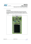
The STM32F401 Discovery kit (32F401CDISCOVERY) helps you to discover the entry level
of the STM32F4 series and to develop your applications. It is based on an
STM32F401VCT6 and includes an ST-LINK/V2 embedded debug tool interface, ST MEMS
Gyroscope, ST MEMS accelerometer + magnetometer, ST MEMS digital microphone, audio
DAC with integrated class D speaker driver, LEDs, pushbuttons and a USB OTG micro-AB
connector.
Figure 1. STM32F401 Discovery board
September 2013
DocID025174 Rev 1
1/39
www.st.com
Contents
UM1669
Contents
1
Conventions . . . . . . . . . . . . . . . . . . . . . . . . . . . . . . . . . . . . . . . . . . . . . . . . 6
2
Quick start . . . . . . . . . . . . . . . . . . . . . . . . . . . . . . . . . . . . . . . . . . . . . . . . . 7
2.1
Getting started . . . . . . . . . . . . . . . . . . . . . . . . . . . . . . . . . . . . . . . . . . . . . . 7
2.2
System requirements . . . . . . . . . . . . . . . . . . . . . . . . . . . . . . . . . . . . . . . . . 7
2.3
Development toolchain supporting the STM32F401 Discovery kit . . . . . . . 7
2.4
Order code . . . . . . . . . . . . . . . . . . . . . . . . . . . . . . . . . . . . . . . . . . . . . . . . . 7
3
Features . . . . . . . . . . . . . . . . . . . . . . . . . . . . . . . . . . . . . . . . . . . . . . . . . . . 8
4
Hardware layout . . . . . . . . . . . . . . . . . . . . . . . . . . . . . . . . . . . . . . . . . . . . 9
4.1
STM32F401VCT6 microcontroller . . . . . . . . . . . . . . . . . . . . . . . . . . . . . . 12
4.2
Embedded ST-LINK/V2 . . . . . . . . . . . . . . . . . . . . . . . . . . . . . . . . . . . . . . 15
4.2.1
Using ST-LINK/V2 to program/debug the STM32F401 on board . . . . . 16
4.2.2
Using ST-LINK/V2 to program/debug an external STM32 application . . 17
4.3
Power supply and power selection . . . . . . . . . . . . . . . . . . . . . . . . . . . . . . 18
4.4
LEDs . . . . . . . . . . . . . . . . . . . . . . . . . . . . . . . . . . . . . . . . . . . . . . . . . . . . 18
4.5
Pushbuttons . . . . . . . . . . . . . . . . . . . . . . . . . . . . . . . . . . . . . . . . . . . . . . . 18
4.6
On board audio capability . . . . . . . . . . . . . . . . . . . . . . . . . . . . . . . . . . . . . 19
4.7
USB OTG supported . . . . . . . . . . . . . . . . . . . . . . . . . . . . . . . . . . . . . . . . 19
4.8
E-compass MEMS (ST MEMS LSM303DLHC) . . . . . . . . . . . . . . . . . . . . 19
4.9
Gyroscope MEMS (ST MEMS L3GD20) . . . . . . . . . . . . . . . . . . . . . . . . . 19
4.10
JP2 (Idd) . . . . . . . . . . . . . . . . . . . . . . . . . . . . . . . . . . . . . . . . . . . . . . . . . . 20
4.11
OSC clock . . . . . . . . . . . . . . . . . . . . . . . . . . . . . . . . . . . . . . . . . . . . . . . . 20
4.11.1
OSC clock supply . . . . . . . . . . . . . . . . . . . . . . . . . . . . . . . . . . . . . . . . . 20
4.11.2
OSC 32 KHz clock supply . . . . . . . . . . . . . . . . . . . . . . . . . . . . . . . . . . . 20
4.12
Solder bridges . . . . . . . . . . . . . . . . . . . . . . . . . . . . . . . . . . . . . . . . . . . . . 21
4.13
Extension connectors . . . . . . . . . . . . . . . . . . . . . . . . . . . . . . . . . . . . . . . . 22
5
Mechanical drawing . . . . . . . . . . . . . . . . . . . . . . . . . . . . . . . . . . . . . . . . 30
6
Electrical schematics . . . . . . . . . . . . . . . . . . . . . . . . . . . . . . . . . . . . . . . 31
2/39
DocID025174 Rev 1
UM1669
7
Contents
Revision history . . . . . . . . . . . . . . . . . . . . . . . . . . . . . . . . . . . . . . . . . . . 37
DocID025174 Rev 1
3/39
3
List of tables
UM1669
List of tables
Table 1.
Table 2.
Table 3.
Table 4.
Table 5.
Table 6.
Table 7.
4/39
ON/OFF conventions . . . . . . . . . . . . . . . . . . . . . . . . . . . . . . . . . . . . . . . . . . . . . . . . . . . . . . 6
Features and benefits . . . . . . . . . . . . . . . . . . . . . . . . . . . . . . . . . . . . . . . . . . . . . . . . . . . . . 12
Jumper states . . . . . . . . . . . . . . . . . . . . . . . . . . . . . . . . . . . . . . . . . . . . . . . . . . . . . . . . . . . 15
Debug connector CN2 (SWD) . . . . . . . . . . . . . . . . . . . . . . . . . . . . . . . . . . . . . . . . . . . . . . 17
Solder bridges. . . . . . . . . . . . . . . . . . . . . . . . . . . . . . . . . . . . . . . . . . . . . . . . . . . . . . . . . . . 21
MCU pin description versus board function . . . . . . . . . . . . . . . . . . . . . . . . . . . . . . . . . . . . 22
Document revision history . . . . . . . . . . . . . . . . . . . . . . . . . . . . . . . . . . . . . . . . . . . . . . . . . 37
DocID025174 Rev 1
UM1669
List of figures
List of figures
Figure 1.
Figure 1.
Figure 2.
Figure 3.
Figure 4.
Figure 5.
Figure 6.
Figure 7.
Figure 8.
Figure 9.
Figure 10.
Figure 11.
Figure 12.
Figure 13.
Figure 14.
Figure 15.
STM32F401 Discovery board . . . . . . . . . . . . . . . . . . . . . . . . . . . . . . . . . . . . . . . . . . . . . . . . 1
Hardware block diagram . . . . . . . . . . . . . . . . . . . . . . . . . . . . . . . . . . . . . . . . . . . . . . . . . . . . 9
Top layout . . . . . . . . . . . . . . . . . . . . . . . . . . . . . . . . . . . . . . . . . . . . . . . . . . . . . . . . . . . . . . 10
Bottom layout . . . . . . . . . . . . . . . . . . . . . . . . . . . . . . . . . . . . . . . . . . . . . . . . . . . . . . . . . . . 11
STM32F401VCT6 microcontroller . . . . . . . . . . . . . . . . . . . . . . . . . . . . . . . . . . . . . . . . . . . 12
STM32F401VCT6 block diagram . . . . . . . . . . . . . . . . . . . . . . . . . . . . . . . . . . . . . . . . . . . 14
Typical configuration . . . . . . . . . . . . . . . . . . . . . . . . . . . . . . . . . . . . . . . . . . . . . . . . . . . . . . 15
STM32F401 Discovery board connections image . . . . . . . . . . . . . . . . . . . . . . . . . . . . . . . 16
ST-Link connections image . . . . . . . . . . . . . . . . . . . . . . . . . . . . . . . . . . . . . . . . . . . . . . . . 17
STM32F401 Discovery board mechanical drawing . . . . . . . . . . . . . . . . . . . . . . . . . . . . . . 30
STM32F401 Discovery board . . . . . . . . . . . . . . . . . . . . . . . . . . . . . . . . . . . . . . . . . . . . . . . 31
ST-LINK/V2 (SWD only) . . . . . . . . . . . . . . . . . . . . . . . . . . . . . . . . . . . . . . . . . . . . . . . . . . . 32
STM32F401VCT6 MCU . . . . . . . . . . . . . . . . . . . . . . . . . . . . . . . . . . . . . . . . . . . . . . . . . . . 33
Audio. . . . . . . . . . . . . . . . . . . . . . . . . . . . . . . . . . . . . . . . . . . . . . . . . . . . . . . . . . . . . . . . . . 34
USB_OTG_FS . . . . . . . . . . . . . . . . . . . . . . . . . . . . . . . . . . . . . . . . . . . . . . . . . . . . . . . . . . 35
Peripherals . . . . . . . . . . . . . . . . . . . . . . . . . . . . . . . . . . . . . . . . . . . . . . . . . . . . . . . . . . . . . 36
DocID025174 Rev 1
5/39
5
Conventions
1
UM1669
Conventions
Table 1 provides the definition of some conventions used in the present document.
Table 1. ON/OFF conventions
Convention
6/39
Definition
Jumper JPx ON
Jumper fitted
Jumper JPx OFF
Jumper not fitted
Solder bridge SBx ON
SBx connections closed by solder
Solder bridge SBx OFF
SBx connections left open
DocID025174 Rev 1
UM1669
2
Quick start
Quick start
The STM32F401 Discovery is a low-cost and easy-to-use development kit to quickly
evaluate and start a development with an STM32F4 entry level microcontroller.
Before installing and using the product, please accept the Evaluation Product License
Agreement from www.st.com/stm32f4-discovery.
For more information on the STM32F401 Discovery board and for demonstration software,
visit www.st.com/stm32f4-discovery.
2.1
Getting started
Follow the sequence below to configure the STM32F401 Discovery board and launch the
DISCOVER application:
2.2
2.3
2.4
1.
Ensure that the jumpers JP2 and CN3 are set to "on" (Discovery mode).
2.
Connect the STM32F401 Discovery board to a PC using a USB cable type A/mini-B
through the USB ST-LINK connector CN1, to power the board. The LED LD2 (PWR)
will light up and the four LEDs between the buttons B1 and B2 start blinking.
3.
Press the user button B1 to enable the MEMS sensor. The four LEDs will indicate the
board motion direction and speed. When connected to a PC with a second USB type
A/micro-B cable through CN5, the board will be recognized as a standard mouse.
4.
The demo software, as well as other software examples that allow you to discover the
STM32 F4 series features, are available on www.st.com/stm32f4-discovery.
5.
Develop your own applications starting from the examples.
System requirements
•
Windows PC (XP, Vista, 7)
•
USB type A to mini-B cable
Development toolchain supporting the STM32F401
Discovery kit
•
Altium: TASKING™ VX-Toolset
•
Atollic: TrueSTUDIO
•
IAR: EWARM
•
Keil™: MDK-ARM
Order code
To order the STM32F401 Discovery kit, use the STM32F401C-DISCO order code.
DocID025174 Rev 1
7/39
37
Features
3
UM1669
Features
The STM32F401 Discovery board offers the following features:
8/39
•
STM32F401VCT6 microcontroller featuring 256 KB of Flash memory, 64 KB of RAM in
an LQFP100 package
•
On-board ST-LINK/V2 with selection mode switch to use the kit as a standalone STLINK/V2 (with SWD connector for programming and debugging)
•
Board power supply: through USB bus or from an external 5 V supply voltage
•
External application power supply: 3 V and 5 V
•
L3GD20, ST MEMS motion sensor, 3-axis digital output gyroscope.
•
LSM303DLHC, ST MEMS system-in-package featuring a 3D digital linear acceleration
sensor and a 3D digital magnetic sensor.
•
MP45DT02, ST MEMS audio sensor, omnidirectional digital microphone
•
CS43L22, audio DAC with integrated class D speaker driver
•
Eight LEDs:
–
LD1 (red/green) for USB communication
–
LD2 (red) for 3.3 V power on
–
Four user LEDs:
LD3 (orange), LD4 (green), LD5 (red) and LD6 (blue)
–
Two USB OTG LEDs:
LD7 (green) VBus and LD8 (red) over-current
•
Two pushbuttons (user and reset)
•
USB OTG with micro-AB connector
•
Extension header for LQFP100 I/Os for a quick connection to the prototyping board
and an easy probing
DocID025174 Rev 1
UM1669
Hardware layout
The STM32F401 Discovery board has been designed around the STM32F401VCT6
microcontroller in a 100-pin LQFP package.
Figure 1 illustrates the connections between the STM32F401VCT6 and its peripherals (STLINK/V2, pushbutton, LED, Audio DAC, USB, ST MEMS gyroscope, ST MEMS
accelerometer + magnetometer, ST MEMS microphone, and connectors).
Figure 2 and Figure 3 help you to locate these features on the STM32F401 Discovery
board.
Figure 1. Hardware block diagram
Mini-USB
SWD
Embedded
ST-LINK/V2
STM32F401VCT6
I/O
I/O
RESET
LEDs
LD3...LD8
B2
RESET
MP45DT02
B1
USER
L3GD20
CS43L22
Mini-Jack
Header
I/O
Header
4
Hardware layout
Micro-USB
LSM303DLHC
MS31947V2
DocID025174 Rev 1
9/39
37
Hardware layout
UM1669
Figure 2. Top layout
ST-LINK/V2
LD2 (red LED)
PWR
LD1 (red/green LED)
COM
CN2
SWD connector
CN3
ST-LINK/DISCOVERY selector
5 V power supply input/output
3 V power supply output
JP2
IDD measurement
SB1 (B2-RESET)
STM32F401VCT6
LD3 (orange LED)
B2 reset button
B1 user button
LD5 (red LED)
LD4 (green LED)
LD6 (blue LED)
LD7 (green LED)
LD8 (red LED)
MS32361V1
10/39
DocID025174 Rev 1
UM1669
Hardware layout
Figure 3. Bottom layout
SB2, SB4, SB6, SB8
(RESERVED)
SB3, SB5, SB7, SB9
(DEFAULT)
SB10, SB11 (RX, TX)
SB15 (SWO)
SB16 (X2 crystal)
SB17 (X3 crystal)
SB12 (STM_RST)
SB18 (X3 crystal)
SB13 (NRST)
SB14 (X2 crystal)
SB19 (BOOT0)
SB20 (BOOT1)
SB21 (B1-USER)
MS32362V1
DocID025174 Rev 1
11/39
37
Hardware layout
4.1
UM1669
STM32F401VCT6 microcontroller
This ARM Cortex-M4 32-bit MCU with FPU has 105 DMIPS, up to 256 KB Flash/64 KB
RAM, USB OTG FS, 10 TIMs, 1 ADC, 11 comm. interfaces.
Figure 4. STM32F401VCT6 microcontroller
STM32F401VCT6
256 Kbytes of Flash memory
64 Kbytes of RAM
LQFP100 14 x 14 mm
MS32365V1
This device provides the following benefits (see Table 2).
Table 2. Features and benefits
Features
Benefits
–
–
High performance
– Up to 84 MHz/105 DMIPS Cortex-M4 with single cycle –
DSP MAC and floating point unit
–
– CoreMark: 285 at 84 MHz
–
– CoreMark/MHz:3.39
–
–
Boosted execution of control algorithms
More features for your applications
Ease of use
Better code efficiency
Faster time to market
Elimination of scaling and saturation
Easier support for meta-language tools
Maximum integration
– Up to 256 kB of on-chip Flash, 64k B of SRAM, reset
circuit, internal RCs, PLLs, ultra-small packages
(WLCSP)
More features in space-constrained applications
Designed for high performance and ultra-fast data
transfers
– ART Accelerator™: memory accelerator
Performance equivalent to zero-wait execution from
Flash
– 32-bit 7-layer bus matrix with 6 masters and 5 slaves
including 1 block of SRAM
– Multi DMA controllers: 2 general-purpose
Concurrent execution and data transfer
Outstanding power efficiency
– Ultra-low dynamic power in Run mode: 140 µA/MHz at
84 MHz running CoreMark benchmark from Flash
memory (peripherals off)
– RTC <1 µA typ in VBAT mode
– Down to 11 µA typ in Stop mode
– 3.6 V down to 1.7 V VDD
– 1.2 V voltage regulator with power scaling capability
Extra flexibility to reduce power consumption for
applications requiring both high-processing and lowpower performance when running at low voltage or on a
rechargeable battery
12/39
DocID025174 Rev 1
UM1669
Hardware layout
Table 2. Features and benefits (continued)
Features
Benefits
Superior and innovative peripherals and
connectivity
– 1x USB OTG
– Up to 11 communication interfaces (including
3x USART, 4x SPI, 3x I2C with digital filter, 1 SDIO)
– USART at up to 10.5 Mbit/s
– SPI at up to 42 Mbit/s
New possibilities to connect and communicate highspeed data
Audio:
– dedicated audio PLL, 2x I2S
High-quality audio support
Analog:
– 1 x 12-bit ADC reaching 2.4 MSPS
– Up to 10 timers: 16 and 32 bits running up to 84 MHz
More precision thanks to high resolution
High integration
– WLCSP49 3 x 3 mm (STM32F401, 256-Kbyte Flash/
64-Kbyte SRAM)
Smaller board space allowing for smaller applications
Extensive tools and software solutions
– Hardware sector protection with execute only access
– Various IDE, starter kits, libraries, RTOS and stacks,
either open source or provided by ST or 3rd parties,
including the ARM CMSIS DSP library optimized for
Cortex-M4 instructions
– Software IP protection
– A wide choice within the STM32 ecosystem to develop
your applications
DocID025174 Rev 1
13/39
37
Hardware layout
UM1669
Figure 5. STM32F401VCT6 block diagram
JTAG & SW
ETM
MPU
NVIC
D-BUS
DMA2
8 Streams
FIFO
DMA1
8 Streams
FIFO
Flash
up to
256 KB
SRAM 64 KB
AHB2 84 MHz
USB
OTG FS
AHB1 84 MHz
Power managmt
Voltage
regulator
3.3 to 1.2 V
VDD
@VDD
@VDDA
PA[15:0]
PB[15:0]
GPIO PORT A
GPIO PORT B
PC[15:0]
GPIO PORT C
PD[15:0]
GPIO PORT D
PE[15:0]
GPIO PORT E
FIFO
S-BUS
ACCEL/
CACHE
FPU
PHY
ARM Cortex-M4
84 MHz
I-BUS
AHB bus-matrix 7S4M
NJTRST, JTDI,
JTCK/SWCLK
JTDO/SWD, JTDO
TRACECLK
TRACED[3:0]
RC HS
POR
reset
RC LS
Int
PLL1&2
Supply
supervision
POR/PDR
BOR
PVD
DP
DM
ID, VBUS, SOF
VDD = 1.7 to 3.6 V
(PDR OFF)
1.8 to 3.6 V
VSS (PDR ON)
VCAP
VDDA, VSSA
NRST
@VDDA @VDD
GPIO PORT H
4 compl. channels TIM1_CH1[1:4]N,
4 channels TIM1_CH1[1:4]ETR,
BKIN as AF
SDIO / MMC
AWU
Backup register
16b
1 channel as AF
TIM10
16b
TIM11
16b
LS
AHB/APB2 AHB/APB1
32b
4 channels, ETR as AF
TIM3
16b
4 channels, ETR as AF
TIM4
16b
4 channels, ETR as AF
TIM5
32b
4 channels
USART2 irDA
RX, TX as AF
CTS, RTS as AF
SP2/I2S2
MOSI/SD, MISO/SD_ext, SCK/CK
NSS/WS, MCK as AF
SP3/I2S3
MOSI/SD, MISO/SD_ext, SCK/CK
NSS/WS, MCK as AF
smcard
USART6
irDA
APB2 60MHz
SPI1
APB1
30MHz
APB1 42
MHz
(max)
smcard
USART1
irDA
MOSI, MISO,
SCK, NSS as AF
MOSI, MISO,
SCK, NSS as AF
VDDREF_ADC
WWDG
APB2 84 MHz
1 channel as AF
16 analog inputs
STAMP1
TIM2
smcard
TIM9
RX, TX, CK as AF
ALARM_OUT
TIM1 / PWM 16b
2 channels as AF
RX, TX, CK,
CTS, RTS as AF
OSC32_IN
OSC32_OUT
DMA1
EXT IT. WKUP
FIFO
D[7:0]
CMD, CK as AF
XTAL 32 kHz
RTC
LS
DMA2
VBAT = 1.65 to 3.6 V
@VBAT
CRC
up to 81 AF
OSC_IN
OSC_OUT
WDG 32K
PWR
interface
HCLK
APB2CLK
APB1CLK
AHB2PCLK
AHB1PCLK
PH[1:0]
XTAL OSC
4- 16MHz
Reset &
clock
MANAGT
control
SPI4
I2C1/SMBUS
SCL, SDA, SMBA as AF
I2C2/SMBUS
SCL, SDA, SMBA as AF
I2C3/SMBUS
SCL, SDA, SMBA as AF
USART
2MBps
Temperature
sensor
ADC1
IF
@VDDA
MS31144V2
14/39
DocID025174 Rev 1
UM1669
4.2
Hardware layout
Embedded ST-LINK/V2
The ST-LINK/V2 programming and debugging tool is integrated on the STM32F401
Discovery board. The embedded ST-LINK/V2 can be used in 2 different ways according to
the jumper states (see Table 3):
•
Program/debug the MCU on board,
•
Program/debug an MCU in an external application board using a cable connected to
SWD connector CN2.
The embedded ST-LINK/V2 supports only SWD for STM32 devices. For information about
debugging and programming features, refer to user manual UM1075 (ST-LINK/V2 in-circuit
debugger/programmer for STM8 and STM32) which describes in detail all the ST-LINK/V2
features.
Figure 6. Typical configuration
Hardware requirements:
- USB cable type A to mini-B
- Computer with Windows XP, Vista or 7
Development toolchains:
- Altium TASKING VX-Toolset
- Atollic TrueSTUDIO
- IAR EWARM
- Keil MDK-ARM
MS31115V1
Table 3. Jumper states
Jumper state
Description
Both CN3 jumpers ON
ST-LINK/V2 functions enabled for on board programming (default)
Both CN3 jumpers OFF
ST-LINK/V2 functions enabled for application through external
CN2 connector (SWD supported)
DocID025174 Rev 1
15/39
37
Hardware layout
4.2.1
UM1669
Using ST-LINK/V2 to program/debug the STM32F401 on board
To program the STM32F401 on board, simply plug in the two jumpers on CN3, as shown in
Figure 7 in red, but do not use the CN2 connector as that could disturb communication with
the STM32F401VCT6 of the STM32F401 Discovery board.
Figure 7. STM32F401 Discovery board connections image
16/39
DocID025174 Rev 1
UM1669
4.2.2
Hardware layout
Using ST-LINK/V2 to program/debug an external STM32 application
It is very easy to use the ST-LINK/V2 to program the STM32 on an external application.
Simply remove the 2 jumpers from CN3 as shown in Figure 8, and connect your application
to the CN2 debug connector according to Table 4.
Note:
SB13 must be OFF if you use CN2 pin 5 in your external application.
Table 4. Debug connector CN2 (SWD)
Pin
CN2
Designation
1
VDD_TARGET
VDD from application
2
SWCLK
SWD clock
3
GND
Ground
4
SWDIO
SWD data input/output
5
NRST
RESET of target MCU
6
SWO
Reserved
Figure 8. ST-Link connections image
DocID025174 Rev 1
17/39
37
Hardware layout
4.3
UM1669
Power supply and power selection
The power supply is provided either by the host PC through the USB cable, or by an
external 5 V power supply.
The D1 and D2 diodes protect the 5 V and 3 V pins from external power supplies:
4.4
4.5
18/39
•
5 V and 3 V can be used as output power supplies when another application board is
connected to pins P1 and P2.
In this case, the 5 V and 3 V pins deliver a 5 V or 3 V power supply and the power
consumption must be lower than 100 mA.
•
5 V can also be used as input power supplies, e.g. when the USB connector is not
connected to the PC.
In this case, the STM32F401 Discovery board must be powered by a power supply unit
or by an auxiliary equipment complying with standard EN-60950-1: 2006+A11/2009,
and must be Safety Extra Low Voltage (SELV) with limited power capability.
LEDs
•
LD1 COM:
LD1 default status is red. LD1 turns to green to indicate that communications are in
progress between the PC and the ST-LINK/V2.
•
LD2 PWR:
The red LED indicates that the board is powered.
•
User LD3:
The orange LED is a user LED connected to the I/O PD13 of the STM32F401VCT6.
•
User LD4:
The green LED is a user LED connected to the I/O PD12 of the STM32F401VCT6.
•
User LD5:
The red LED is a user LED connected to the I/O PD14 of the STM32F401VCT6.
•
User LD6:
The blue LED is a user LED connected to the I/O PD15 of the STM32F401VCT6.
•
USB LD7:
The green LED indicates when VBUS is present on CN5 and is connected to PA9 of
the STM32F401VCT6.
•
USB LD8:
The red LED indicates an overcurrent from VBUS of CN5 and is connected to the I/O
PD5 of the STM32F401VCT6.
Pushbuttons
•
B1 USER:
User and Wake-Up button connected to the I/O PA0 of the STM32F401VCT6.
•
B2 RESET:
The pushbutton connected to NRST is used to RESET the STM32F401VCT6.
DocID025174 Rev 1
UM1669
4.6
Hardware layout
On board audio capability
The STM32F401 uses an audio DAC (CS43L22) to output sounds through the audio mini
jack connector.
The STM32F401 controls the audio DAC through the I2C interface and processes digital
signals through an I2S connection or analog input signal.
•
•
4.7
The sound can come independently from different inputs:
–
ST MEMS microphone (MP45DT02): digital using PDM protocol or analog when
using the low pass filter.
–
USB connector: from external mass storage such as a USB key, USB HDD, and
so on.
–
Internal memory of the STM32F401.
The sound can be output in different ways through audio DAC:
–
Using the I2S protocol
–
Using the microphone output directly via a low pass filter to analog input AIN4x of
the CS43L22
USB OTG supported
The STM32F401 is used to drive only USB OTG full speed on this board. The USB microAB connector (CN5) allows the user to connect a host or device component, such as a USB
key, mouse, and so on.
Two LEDs are dedicated to this module:
4.8
•
LD7 (green LED) indicates when VBUS is active
•
LD8 (red LED) indicates an overcurrent from a connected device.
E-compass MEMS (ST MEMS LSM303DLHC)
The LSM303DLHC is an ultra-compact low-power system-in-package featuring a 3D digital
linear acceleration sensor and a 3D digital magnetic sensor. It includes a sensing element
and an IC interface able to provide the measured acceleration to the external world through
an I2C serial interface.
The LSM303DLHC has dynamically user-selectable full scales of ± 2g/± 8g and is capable
of measuring the acceleration, and a magnetic field full scale from ±1.3 g to 8.1 g with an
output data rate of 100 Hz or 400 Hz.
The STM32F401VCT6 MCU controls this motion sensor through the I2C interface.
4.9
Gyroscope MEMS (ST MEMS L3GD20)
The L3GD20 is an ultra-compact, low-power, three-axis angular rate sensor. It includes a
sensing element and an IC interface able to provide the measured angular rate to the
external world through the I2C/SPI serial interface.
The L3GD20 has dynamically user-selectable full scales of ± 250 dps/500 dps/±2000 dps
and is capable of measuring rates.
DocID025174 Rev 1
19/39
37
Hardware layout
UM1669
The STM32F401VCT6 MCU controls this motion sensor through the SPI interface.
4.10
JP2 (Idd)
Jumper JP2, labeled Idd, allows the consumption of STM32F401VCT6 to be measured by
removing the jumper and connecting an ammeter.
•
Jumper on: STM32F401VCT6 is powered (default).
•
Jumper off: an ammeter must be connected to measure the STM32F401VCT6 current,
(if there is no ammeter, the STM32F401VCT6 is not powered).
4.11
OSC clock
4.11.1
OSC clock supply
If PH0 and PH1 are only used as GPIOs instead of as a clock, then SB14 and SB16 are
closed and R24, R25 and R66 are removed.
MCO from ST-LINK (from MCO of the STM32F103)
This frequency cannot be changed, it is fixed at 8 MHz and connected to PH0-OSC_IN of
the STM32F401VCT6. The configuration needed is:
–
SB14, SB16 OPEN
–
R25 removed
–
R66 soldered
Oscillator onboard (from X2 crystal)
For typical frequencies and its capacitors and resistors, please refer to the
STM32F401VCT6 Datasheet. The configuration needed is:
–
SB14, SB16 OPEN
–
R25 soldered
–
R66 removed
Oscillator from external PH0 (from external oscillator through pin 7 of the P2 connector)
The configuration needed is:
4.11.2
–
SB14 closed
–
SB16 closed
–
R25 and R66 removed
OSC 32 KHz clock supply
If PC14 and PC15 are only used as GPIOs instead of as a clock, then SB17 and SB18 are
closed, and R21 and R22 are removed.
Oscillator onboard (from X1 Crystal (not provided))
The configuration needed is:
20/39
–
SB17, SB18 OPEN
–
C20, C28, R21 and R22 soldered
DocID025174 Rev 1
UM1669
Hardware layout
Oscillator from external PC14 (from external oscillator trough the pin 9 of P2 connector)
The configuration needed is:
4.12
–
SB17closed
–
SB18 closed
–
R21 and R22 removed
Solder bridges
Table 5. Solder bridges
Bridge
State
X2, C18, C19, R24 and R25 provide a clock.
PH0, PH1 are disconnected from P2
ON
PH0, PH1 are connected to P2
R24, R25 and R66 must not be fitted).
ON
Reserved, do not modify
SB2,4,6,8 (Reserved) OFF
SB17,18 (X3 crystal)
SB1 (B2-RESET)
SB21 (B1-USER)
SB10,11 (RX,TX)
SB12 (STM_RST)
Reserved, do not modify
OFF
X3, C20, C28, R21 and R22 deliver a 32 KHz clock.
PC14, PC15 are not connected to P2.
ON
PC14, PC15 are only connected to P2. Remove only R21, R22
ON
B2 pushbutton is connected to the NRST pin of the STM32F401VCT6 MCU
OFF
B2 pushbutton is not connected to the NRST pin of the STM32F401VCT6 MCU
ON
B1 pushbutton is connected to PA0
OFF
B1 pushbutton is not connected to PA0
ON
NRST signal of the CN2 connector is connected to the NRST pin of the
STM32F401VCT6 MCU
OFF
NRST signal of the CN2 connector is not connected to the NRST pin of the
STM32F401VCT6 MCU
ON
SWO signal of the CN2 connector is connected to PB3
OFF
SWO signal is not connected
OFF
Reserved, do not modify
ON
Reserved, do not modify
OFF
No incidence on STM32F103C8T6 (ST-LINK/V2) NRST signal
ON
STM32F103C8T6 (ST-LINK/V2) NRST signal is connected to GND
ON
BOOT0 signal of the STM32F401VCT6 MCU is held low through a 510 Ω pulldown resistor
OFF
BOOT0 signal of the STM32F401VCT6 MCU is held high through a 10 KΩ pullup resistor
OFF
The BOOT1 signal of the STM32F401VCT6 MCU is held high through a 10 KΩ
pull-up resistor
ON
The BOOT1 signal of the STM32F401VCT6 MCU is held low through a 510 Ω
pull-down resistor
SB13 (NRST)
SB15 (SWO)
Description
OFF
SB14,16 (X2 crystal)
SB3,5,7,9 (Default)
(1)
SB19 (BOOT0)
SB20 (BOOT1)
DocID025174 Rev 1
21/39
37
Hardware layout
UM1669
1. Default SBx state is shown in bold.
4.13
Extension connectors
The male headers P1 and P2 can connect the STM32F401 Discovery board to a standard
prototyping/wrapping board. STM32F401VCT6 GPI/Os are available on these connectors.
P1 and P2 can also be probed by an oscilloscope, logical analyzer or voltmeter.
Table 6. MCU pin description versus board function (page 1 of 8)
5
6
TIM2_CH1/TIM2_ETR,
TIM5_CH1,
USART2_CTS,
ADC1_0, WKUP
23
PA1
TIM2_CH2, TIM5_CH2,
USART2_RTS,
ADC1_1
24
11
PA2
TIM2_CH3, TIM5_CH3,
TIM9_CH1,
USART2_TX, ADC1_2
25
14
PA3
TIM2_CH4, TIM5_CH4,
TIM9_CH2,
USART2_RX, ADC1_3
26
13
PA4
SPI1_NSS,
SPI3_NSS/I2S3_WS,
USART2_CK, ADC1_4
29
PA5
TIM2_CH1/TIM2_ETR,
SPI1_SCK, ADC1_5
30
15
PA6
TIM1_BKIN,
TIM3_CH1,
SPI1_MISO, ADC1_6
31
18
LRCK/AIN1x
PA0WKUP
22/39
P2
P1
CN2
CN5
Power supply
Free I/O
OSC
USB
SWD
NRST
14
LED
Pushbutton
NRST
RESET
21
SCL/SPC
94
SDO
BOOT0
USER
LSM303DLHC
L3GD20
MP45DT02
Alternate
functions
CS43L22
Main
function
Board function
LQFP100
MCU pin
12
16
DocID025174 Rev 1
UM1669
Hardware layout
Table 6. MCU pin description versus board function (page 2 of 8)
PA11
TIM1_CH4,
USART1_CTS,
USART6_TX,
USB_FS_DM
70
PA12
TIM1_ETR,
USART1_RTS,
USART6_RX,
USB_FS_DP
71
3
PA13
JTMS-SWDIO
72
PA14
JTCK-SWCLK,
I2S3ext_WS
76
PA15
JTDI,
TIM2_CH1/TIM2_ETR,
SPI1_NSS,
SPI3_NSS/I2S3_WS
77
PB0
TIM1_CH2N,
TIM3_CH3, ADC1_8
35
SDA/SDI/SDO
P2
69
P1
TIM1_CH3,
USART1_RX,
USB_FS_ID
CN5
PA10
CN2
Power supply
68
Free I/O
PA9
TIM1_CH2,
I2C3_SMBAL,
USART1_TX,
USB_FS_VBUS
OSC
67
USB
PA8
MCO_1, TIM1_CH1,
I2C3_SCL,
USART1_CK,
USB_FS_SOF
SWD
32
LED
TIM1_CH1N,
TIM3_CH2,
SPI1_MOSI, ADC1_7
DP
Pushbutton
PA7
L3GD20
Alternate
functions
17
SWCLK SWDIO
VBUS
1
44
ID
4
41
DM
43
GREEN
CS43L22
Main
function
LQFP100
LSM303DLHC
Board function
MP45DT02
MCU pin
2
4
42
2
39
40
22
DocID025174 Rev 1
23/39
37
Hardware layout
UM1669
Table 6. MCU pin description versus board function (page 3 of 8)
PB4
JTRST, TIM3_CH1,
SPI1_MISO,
90
SPI3_MISO,
I2S3ext_SD, I2C3_SDA
SWO
PB3
JTDO-SWO,
TIM2_CH2, SPI1_SCK,
SPI3_SCK/I2S3_CK,
I2C2_SDA
89
P1
CN2
CN5
Free I/O
24
OSC
37
PB2
USB
21
SWD
36
LED
TIM1_CH3N,
TIM3_CH4, ADC1_9
6
P2
Power supply
Pushbutton
PB1
L3GD20
Alternate
functions
CS43L22
Main
function
LQFP100
LSM303DLHC
Board function
MP45DT02
MCU pin
28
25
PB5
TIM3_CH2,
I2C1_SMBAL,
SPI1_MOSI,
SPI3_MOSI/I2S3_SD
91
PB6
TIM4_CH1, I2C1_SCL,
USART1_TX,
USB_FS_INT
92
PB7
TIM4_CH2, I2C1_SDA,
USART1_RX
93
24
PB8
TIM4_CH3,
TIM10_CH1,
I2C1_SCL,
USB_FS_SCL,
SDIO_D4
95
19
PB9
TIM4_CH4,
TIM11_CH1,
I2C1_SDA,
SPI2_NSS/I2S2_WS,
USB_FS_SDA,
SDIO_D5
96
PB10
TIM2_CH3, I2C2_SCL,
SPI2_SCK/I2S2_CK
47
24/39
SCL
SDA
SCL
20
CLK
SDA
23
34
VDD
VCAP1
26
48
DocID025174 Rev 1
35
UM1669
Hardware layout
Table 6. MCU pin description versus board function (page 4 of 8)
53
38
PB15
RTC_50Hz,
TIM1_CH3N,
SPI2_MOSI/I2S2_SD,
I2S2ext_MISO
54
39
PC0
ADC1_10
15
PC1
ADC1_11
16
7
PC2
SPI2_MISO,
I2S2ext_SD, ADC1_12
17
10
PC3
SPI2_MOSI/I2S2_SD,
ADC1_13
18
PC4
ADC1_14
33
20
PC5
ADC1_15
34
19
TIM3_CH1, I2S2_MCK,
63
USART6_TX, SDIO_D6
PC7
TIM3_CH2, I2S3_MCK,
64
USART6_RX, SDIO_D7
PC8
MCO_CPUCK,
TIM3_CH3,
65
USART6_CK, SDIO_D0
PowerOn
PDM_OUT
AIN4x
8
9
47
MCLK
PC6
P1
TIM1_CH2N,
SPI2_MISO,
I2S2ext_SD
CN2
PB14
CN5
37
Free I/O
52
OSC
TIM1_CH1N,
SPI2_SCK/I2S2_CK,
I2S2ext_CK
USB
PB13
SWD
36
LED
51
P2
Power supply
Pushbutton
PB12
TIM1_BKIN,
I2C2_SMBAL,
SPI2_NSS/I2S2_WS,
I2S2ext_WS
L3GD20
Alternate
functions
CS43L22
Main
function
LQFP100
LSM303DLHC
Board function
MP45DT02
MCU pin
48
45
DocID025174 Rev 1
25/39
37
Hardware layout
UM1669
Table 6. MCU pin description versus board function (page 5 of 8)
PC14
OSC32_IN
8
PC15
OSC32_OUT
9
P2
7
P1
TAMP_1
CN2
PC13
CN5
80
Power supply
I2S3ext_MISO,
SPI3_MOSI/I2S3_SD,
SDIO_CK
Free I/O
PC12
OSC
79
46
37
38
35
12
OSC32_OUT OSC32_IN
I2S3ext_SD,
SPI3_MISO, SDIO_D3
USB
PC11
SWD
78
LED
I2S3ext_CK,
SPI3_SCK/I2S3_CK,
SDIO_D2
Pushbutton
PC10
LSM303DLHC
66
L3GD20
MCO_2, TIM3_CH4,
I2C3_SDA, I2S2_CKIN,
SDIO_D1
MP45DT02
PC9
SCLK
Alternate
functions
SDIN
Main
function
CS43L22
Board function
LQFP100
MCU pin
9
10
PD0
81
36
PD1
82
33
PD2
TIM3_ETR, SDIO_CMD 83
34
PD4
USART2_RTS
85
PD5
USART2_TX
86
PD6
SPI3_MOSI/I2S3_SD,
USART2_RX
87
26/39
31
32
OverCurrent
84
RED
SPI2_SCK/I2S2_CK,
USART2_CTS
RESET
PD3
29
30
DocID025174 Rev 1
UM1669
Hardware layout
Table 6. MCU pin description versus board function (page 6 of 8)
27
55
40
PD9
56
41
PD10
57
42
PD11
58
43
59
TIM4_CH2
60
PD14
TIM4_CH3
61
PD15
TIM4_CH4
62
PE0
TIM4_ETR
97
47
17
18
15
TRACECLK, SPI4_SCK
1
PE3
TRACED0
2
PE4
TRACED1, SPI4_NSS
3
13
PE5
TRACED2, TIM9_CH1,
SPI4_MISO
4
14
PE6
TRACED3, TIM9_CH2,
SPI4_MOSI
5
PE7
TIM1_ETR
38
CS_I2C/SPI
PE2
INT1
98
46
INT2
PE1
45
DRDY
PD13
44
INT2 INT1
TIM4_CH1
BLUE RED ORANGE GREEN
PD8
PD12
P2
P1
CN2
CN5
Power supply
Free I/O
OSC
USB
SWD
LED
88
Pushbutton
USART2_CK
LSM303DLHC
PD7
L3GD20
Alternate
functions
MP45DT02
Main
function
CS43L22
Board function
LQFP100
MCU pin
16
11
25
DocID025174 Rev 1
27/39
37
Hardware layout
UM1669
Table 6. MCU pin description versus board function (page 7 of 8)
TIM1_CH2N
41
28
PE11
TIM1_CH2, SPI4_NSS
42
29
PE12
TIM1_CH3N,
SPI4_SCK
43
30
PE13
TIM1_CH3, SPI4_MISO 44
31
PE14
TIM1_CH4, SPI4_MOSI 45
32
OSC_IN
12
PH1
OSC_OUT
13
28/39
DocID025174 Rev 1
7
8
GND GND GND GND VDD VDD 3 V 3 V 5 V 5 V
PH0
33
OSC_OUT OSC_IN
46
GND
TIM1_BKIN
GND
PE15
P1
PE10
CN2
27
CN5
40
Free I/O
TIM1_CH1
OSC
PE9
USB
26
SWD
39
LED
TIM1_CH1N
P2
Power supply
Pushbutton
PE8
L3GD20
Alternate
functions
CS43L22
Main
function
LQFP100
LSM303DLHC
Board function
MP45DT02
MCU pin
3
4
5
6
3
22
4
5
3
1
1
2
2
5
23
UM1669
Hardware layout
Table 6. MCU pin description versus board function (page 8 of 8)
DocID025174 Rev 1
P1
P2
CN2
CN5
Power supply
GND GND
Free I/O
OSC
USB
SWD
LED
Pushbutton
LSM303DLHC
L3GD20
MP45DT02
Alternate
functions
CS43L22
Main
function
Board function
LQFP100
MCU pin
49
49
50
50
29/39
37
Mechanical drawing
5
UM1669
Mechanical drawing
Figure 9. STM32F401 Discovery board mechanical drawing
30/39
DocID025174 Rev 1
TM32F4_USART2_TX
TM32F4_USART2_RX
VDD
PA9
PA10
PA11
PA12
PA2
PA3
NRST
PB3
MCO
PA14
PA13
DocID025174 Rev 1
PE7
PE9
PE11
PE13
PE15
NC
PB13
PB15
PD9
PD11
PD13
PD15
PC1
PC3
PA1
PA3
PA5
PA7
PC5
PB1
PA9
PA10
PA11
PA12
2
4
6
8
10
12
14
16
18
20
22
24
26
28
30
32
34
36
38
40
42
44
46
48
50
Header 25X2
1
3
5
7
9
11
13
15
17
19
21
23
25
27
29
31
33
35
37
39
41
43
45
47
49
P1
PD5
PC0
U_USB_OTG_FS
USB_OTG_FS.SchDoc
PA2
PA3
NRST
PC0
PC2
PA0
PA2
PA4
PA6
PC4
PB0
PB2
PE8
PE10
PE12
PE14
PB10
PB12
PB14
PD8
PD10
PD12
PD14
NC
BOOT1 / PB2
VDD
T_NRST
T_SWO
NRST
PB3
PD5
PC0
TCK/SWCLK
TMS/SWDIO
MCO
PA14
PA13
PC0
PC1
PC2
PC3
PC4
PC5
PC6
PC7
PC8
PC9
PC10
PC11
PC12
PC13
PC14
PC15
PB12
PB13
PB14
PB15
PB0
PB1
PB2
PB3
PB4
PB5
PB6
PB7
PB8
PB9
PB10
PA0
PA1
PA2
PA3
PA4
PA5
PA6
PA7
PA8
PA9
PA10
PA11
PA12
PA13
PA14
PA15
PC0
PC1
PC2
PC3
PC4
PC5
PC6
PC7
PC8
PC9
PC10
PC11
PC12
PC13
PC14
PC15
PB12
PB13
PB14
PB15
PB0
PB1
PB2
PB3
PB4
PB5
PB6
PB7
PB8
PB9
PB10
PA0
PA1
PA2
PA3
PA4
PA5
PA6
PA7
PA8
PA9
PA10
PA11
PA12
PA13
PA14
PA15
U_STM32Fx
STM32Fx.SchDoc
NRST
BOOT0
PH0
PH1
MCO
PD0
PD1
PD2
PD3
PD4
PD5
PD6
PD7
PD8
PD9
PD10
PD11
PD12
PD13
PD14
PD15
PE0
PE1
PE2
PE3
PE4
PE5
PE6
PE7
PE8
PE9
PE10
PE11
PE12
PE13
PE14
PE15
NRST
BOOT0
PH0
PH1
MCO
PD0
PD1
PD2
PD3
PD4
PD5
PD6
PD7
PD8
PD9
PD10
PD11
PD12
PD13
PD14
PD15
PE0
PE1
PE2
PE3
PE4
PE5
PE6
PE7
PE8
PE9
PE10
PE11
PE12
PE13
PE14
PE15
3V
5V
3V
PH0
PC14
PE6
PE4
PE2
PE0
PB8
BOOT0
PB6
PB4
PD7
PD5
PD3
PD1
PC12
PC10
PA14
PA10
PA8
PC8
PC6
PB6
PB9
PB10
PC3
PC4
2
4
6
8
10
12
14
16
18
20
22
24
26
28
30
32
34
36
38
40
42
44
46
48
50
PE0
PE1
PE3
PA5
PA6
PA7
PA0
NRST
Header 25X2
1
3
5
7
9
11
13
15
17
19
21
23
25
27
29
31
33
35
37
39
41
43
45
47
49
P2
PB6
PB9
PE2
PE4
PE5
PD12
PD13
PD14
PD15
U_IO Peripherals
IO Peripherals.SchDoc
PA4
PC12
PC10
PD4
PC7
U_Audio
Audio.SchDoc
PB7
PB5
PB3
PD6
PD4
PD2
PD0
PC11
PA15
PA13
PA9
PC9
PC7
5V
3V
PH1
PC15
PC13
PE5
PE3
PE1
PB9
PE0
PE1
PE3
PA5
PA6
PA7
PA0
NRST
PB6
PB9
PB10
PC3
PC4
Date: 8/12/2013
STM32F401C-DISCOVERY
Number:MB1115 Rev: B.1(PCB.SCH)
Title:
STMicroelectronics
5V
Sheet 1
VDD
3V
Rev A.0 --> PCB label MB1115 A-00
Rev B.1 --> PCB label MB1115 B-01 LD3GD20 U7 was routed wrong.
5V
PB6
PB9
PE2
PE4
PE5
PD12
PD13
PD14
PD15
PA4
PC12
PC10
PD4
PC7
6
ST_LINK_V2.SCHDOC
U_ST_LINK
UM1669
Electrical schematics
Electrical schematics
Figure 10. STM32F401 Discovery board
31/39
37
C11
3V
100nF
4K7
R19
USB
1
2
3
4
5
6
USB-MINI-typeB
VCC
DD+
ID
GND
SHELL
CN1
R7
R9
R8
R6
U5V
Close to JP
Not Fitted
VBAT
PC13
PC14
PC15
OSCIN
OSCOUT
NRST
VSSA
VDDA
PA0
PA1
PA2
3V
Not Fitted
STLINK_RX
1
2
3
4
5
6
7
8
9
10
11
12
3V
1K5
3V
0
USB_DM
0
USB_DP
100K
SB10
JP1
AIN_1
SB11
TX
RX
4K7
OSC_IN
OSC_OUT
STM_RST
[NA]
R20
8MHz
STM32F4_USART2_TX
PA2
PA3
C6
20pF X1
20pF
1
2
STM32F4_USART2_RX
SB12
R18
100K
3V
C9
R11
100K
R5
SWIM_IN
SWIM
Board Ident: PC13=0
STLINK_TX
STM_JTCK
SWIM_IN
SWIM_RST
SWIM_RST_IN
48
47
46
45
44
43
42
41
40
39
38
37
C7
100nF
C8
100nF
C12
100nF
5V
C17
1uF
C10
100nF
3V
VDD_2
VSS_2
JTMS/SWDIO
PA12
PA11
PA10
PA9
PA8
PB15
PB14
PB13
PB12
VDD_3
VSS_3
PB9
PB8
BOOT0
PB7
PB6
PB5
PB4/JNTRST
PB3/JTDO
PA15/JTDI
JTCK/SWCLK
PA3
PA4
PA5
PA6
PA7
PB0
PB1
PB2/BOOT1
PB10
PB11
VSS_1
VDD_1
13
14
15
T_JTCK
16
T_JTDO
17
T_JTDI
18
T_NRST
T_JRST 19
20
SWIM_IN 21
22
SWIM
23
24
10K
36
35
34
33
32
31
30
29
28
27
26
25
INH
GND
Vin
U3
100
R66
1
2
3
4
5
6
BYPASS
Vout
5
U5V
R14
10K
R2
R17
R16
R15
R10
22
22
22
22
BAT60JFILM
D2
AIN_1
T_SWO
T_NRST
T_JTMS
T_JTCK
[NA]
C67
20pF
C14
1uF
2V5
C15
100nF
BAT60JFILM
D1
MCO
5V
JP3
JP4
5V
INH
GND
Vin
BYPASS
Vout
LED_STLINK
COM
PWR
CN3
LD3985M33R
C2
C5
100nF
10nF
3
1
U1
T_SWO
SB15
T_NRST
SB8
SB6
SB4
SB2
5
100
R3
100
R4
3
2
C4
1uF
SWDIO
SWCLK
3V
4 R1
0
1
C3
100nF
3V
3V
OUT_3V, Only Output
BAT60JFILM
D3
LD_BICOLOR_CMS
_Green
Red
LD1
SWD
Date: 8/12/2013
Sheet 2
of
6
STM32F401C-DISCOVERY ST-LINK/V2 (SWD only)
Number:MB1115 Rev: B.1(PCB.SCH)
Title:
STM_JTMS
STM_JTCK
SB13
PA14
PA13
NRST
PB3
Jumpers ON --> DISCOVERY Selected
Jumpers OFF --> ST-LINK Selected
SB9
SB7
SB5
SB3
DEFAULT
STMicroelectronics
C1
1uF
Wired on Solder Side
Not Fitted
MCO
RC Must be very close to STM32F103 pin 29
Header 6
CN2
SWD
EXT_5V, Input or Output
VDD
R67
100
LD3985M25R
C16
C13
100nF
10nF
3
1
JP2
LD2
LED, red
R13
1K
3V
Idd
T_SWDIO_IN
T_JTMS
T_JTCK
STM_JTMS
USB_DP
USB_DM
T_SWO
LED_STLINK
3V
U2
STM32F103C8T6
2
R12
4
2
DocID025174 Rev 1
4
1
2
3
4
32/39
RESERVED
TCK/SWCLK
TMS/SWDIO
Electrical schematics
UM1669
Figure 11. ST-LINK/V2 (SWD only)
Ferrite
L1
C30
100nF
VDD
C25
100nF
R27
4.7K
47
C32
100nF
R23
PB6
PB9
R32
4.7K
C26
100nF
VDD
C31
100nF
C24
1uF
C22
1uF
R26
0
C35
100nF
C34
C29
100nF
100nF
C23
100nF
C21
100nF
PC0
PC1
PC2
PC3
PC4
PC5
PC6
PC7
PC8
PC9
PC10
PC11
PC12
PC13
PB12
PB13
PB14
PB15
PB0
PB1
PB2
PB3
PB4
PB5
PB6
PB7
PB8
PB9
PB10
15
16
17
18
33
34
63
64
65
66
78
79
80
7
PC0
PC1
PC2
PC3
PC4
PC5
PC6
PC7
PC8
PC9
PC10
PC11
PC12
PC13
C27
1uF
21
22
6
11
19
28
50
75
100
51
52
53
54
PB12
PB13
PB14
PB15
PC0
PC1
PC2
PC3
PC4
PC5
PC6
PC7
PC8
PC9
PC10
PC11
PC12
PC13
PB12
PB13
PB14
PB15
PB0
PB1
PB2
PB3
PB4
PB5
PB6
PB7
PB8
PB9
PB10
PA0
PA1
PA2
PA3
PA4
PA5
PA6
PA7
PA8
PA9
PA10
PA11
PA12
PA13
PA14
PA15
U4A
BOOT0
NRST
PC14
PC15
PH0
PH1
VSS
PD0
PD1
PD2
PD3
PD4
PD5
PD6
PD7
PD8
PD9
PD10
PD11
PD12
PD13
PD14
PD15
PE0
PE1
PE2
PE3
PE4
PE5
PE6
PE7
PE8
PE9
PE10
PE11
PE12
PE13
PE14
PE15
VSS
VSSA
VCAP1
VCAP2
VSS5
VSS4
VSS2
STM32F401VCT6U
VREF+
VDDA
VBAT
VDD5
VDD12
VDD4
VDD1
VDD2
VDD3
STM32F401VCT6U
U4B
35
36
37
89
90
91
92
93
95
96
47
PB0
PB1
PB2
PB3
PB4
PB5
PB6
PB7
PB8
PB9
PB10
23
24
25
26
29
30
31
32
67
68
69
70
71
72
76
77
49
20
48
73
10
27
74
C38
2.2uF
BOOT0
BOOT0
94
C33
2.2uF
VDD
R29
[NA]
R28
NRST
NRST
14
PD0
PD1
PD2
PD3
PD4
PD5
PD6
PD7
PD8
PD9
PD10
PD11
PD12
PD13
PD14
PD15
PE0
PE1
PE2
PE3
PE4
PE5
PE6
PE7
PE8
PE9
PE10
PE11
PE12
PE13
PE14
PE15
PC14-OSC32_IN
PC15-OSC32_OUT
PD0
PD1
PD2
PD3
PD4
PD5
PD6
PD7
PD8
PD9
PD10
PD11
PD12
PD13
PD14
PD15
PE0
PE1
PE2
PE3
PE4
PE5
PE6
PE7
PE8
PE9
PE10
PE11
PE12
PE13
PE14
PE15
8
9
12
13
99
81
82
83
84
85
86
87
88
55
56
57
58
59
60
61
62
97
98
1
2
3
4
5
38
39
40
41
42
43
44
45
46
SB19
510
SB17
SB18
R31
510
R30
10K
PC15
PC14
PB2
BOOT1
0
R21
0
R22
PH0-OSC_IN
PH1-OSC_OUT
SB20
VDD
C20
R24
0
220
SB16
R25
C18
20pF
C19
20pF
MCO
Date: 8/12/2013
STM32F401C-DISCOVERY MCU
Number:MB1115 Rev: B.1(PCB.SCH)
Title:
STMicroelectronics
6.8pF
PH0
X2
8MHz
SB14
PH1
MCO
Must be close to the Crystal
6.8pF
X3
XTAL_32K_20PPM
C28
Not Fitted
4
1
2
PA0
PA1
PA2
PA3
PA4
PA5
PA6
PA7
PA8
PA9
PA10
PA11
PA12
PA13
PA14
PA15
3
2
DocID025174 Rev 1
1
PA0
PA1
PA2
PA3
PA4
PA5
PA6
PA7
PA8
PA9
PA10
PA11
PA12
PA13
PA14
PA15
Sheet 3
of
6
UM1669
Electrical schematics
Figure 12. STM32F401VCT6 MCU
33/39
37
34/39
Audio_RST
DocID025174 Rev 1
R61
0
R62
[NA]
3V
PD4
1
2
3
10K
R43
VDD
DOUT
CLK
10uF
C65
C44
100nF
MP45DT02
GND
LR
GND
U10
100nF
C66
2V5
PD4
6
5
4
3V
PC3
PB10
C64
1uF
C56
1uF
3V
C46
100nF
PDM_OUT
CLK_IN
37
38
39
40
32
PC7
PC10
PC12
PA4
20
36
33
35
41
13
16
34
12
10
11
1
2
3
PB9
PB6
PC3
PB10
C59
100nF
C52
1uF
PC7
PC10
PC12
PA4
PB9
PB6
C45
100nF
I2S3_MCK
I2S3_SCK
I2S3_SD
I2S3_WS
Audio_SDA
Audio_SCL
CS43L22
I2C address 0x94
VQ
AFILTB
AFILTA
FILT+
AGND
AIN1B
AIN1A
AIN2B
AIN2A
AIN3B
AIN3A
AIN4B
AIN4A
SPKR_OUTA+
SPKR_OUTASPKR_OUTB+
SPKR_OUTBVP
VP
HP/LINE_OUTA
HP/LINE_OUTB
SPKR/HP
TSTO
TSTO
VL
DGND
GND/Thermal Pad
+VHP
VA
VD
FLYP
-VHPFILT
FLYN
MCLK
SCLK
SDIN
LRCK
RESET
SDA
SCL
A0
U8
19
28
27
18
17
30
29
26
25
24
23
22
21
4
6
7
9
8
5
15
14
31
100
R51
100
R45
C62
1uF
1uF
C57
1uF
100K
100K
R50
[NA]
R44
R46
C50
100nF
C53
150pF
C61
22nF
R60
51
C47
C49
100nF
C60
22nF
R59
51
C51
150pF
PA4
3V
3
1
[NA]
R47
PC4
PC4
PDM_OUT
Date: 8/12/2013
STM32F401C-DISCOVERY Audio
Number:MB1115 Rev: B.1(PCB.SCH)
Title:
STMicroelectronics
C63
1uF
0
R53
PC3
ST-225-02
Audio_DAC_OUT
C58
10nF R52
1.2K
0
R63
2 CN4
Sheet 4
of
6
Electrical schematics
UM1669
Figure 13. Audio
VBUS_FS
OTG_FS_DM
OTG_FS_DP
OTG_FS_ID
OTG_FS_PowerSwitchOn
PA9
PA11
PA12
PA10
PC0
PA9
PA11
PA12
PA10
PC0
R57
0
R42
0
B3
C3
D3
A2
B2
5V
R41
10K
3V
22
22
GND
ID
D+in
D-in
Pd1
Pd2
R56
R58
D2
A3
C1
D1
B1
C2
STMPS2141STR
GND FAULT
IN
OUT
EN
EMIF02-USB03F2
Vbus
D+out
D-out
Dz
Pup
U9
2
5
4
U6
3
1
C54
4.7uF
R49
47K
3V
0
R48
LD8
LED, red
R65
620
[NA]
R55
R54
47K
1
6
1
2
3
4
5
USB_Micro-AB receptacle
OTG_FS_OverCurrent
Date: 8/12/2013
Sheet 5
STM32F401C-DISCOVERY USB_OTG_FS
Number:MB1115 Rev: B.1(PCB.SCH)
Title:
STMicroelectronics
USB-MICRO-AB
Shield
VBUS
DM
DP
ID
GND
CN5
PD5
T1
9013-SOT23
LD7
LED, green
R64
330
3V
PD5
3
DocID025174 Rev 1
2
of
6
UM1669
Electrical schematics
Figure 14. USB_OTG_FS
35/39
37
DocID025174 Rev 1
SPI1_SCK
SPI1_MOSI
SPI1_MISO
CS_I2C/SPI
MEMS_INT2
MEMS_INT1
PB6
PB9
PE5
PE4
PA5
PA7
PA6
PE3
PE1
PE0
PB6
PB9
PE5
PE4
PA5
PA7
PA6
PE3
PE1
PE0
C42
4.7uF
1
2
3
4
5
6
7
8
1
2
3
4
5
6
7
L3GD20
VDD
SETC
SETP
GND
GND
DRDY
NC
MEMS
VDD_IO
SCL/SPC
SDA/SDI/SDO
SA0/SDO
CS_I2C/SPI
DRDY/INT2
INT1
GND
U7
LSM303DLHC
VDD_IO
SCL
SDA
INT2
INT1
C1
GND
U5
VDD
VDD
C1
GND
GND
GND
GND
GND
14
13
12
11
10
9
8
3V
16
15
14
13
12
11
10
9
3V
PE2
C41
C48
10nF
PE2
220nF
C55
100nF
C43
10uF
C40
100nF
C37
10uF
PA0
PA0
330
L
USER & WAKE-UP Button
SB21
R34
[NA]
C36
100
VDD
4
1
R35
220K
3
2
SW-PUSH-CMS_BLUE
B1
D
U
PD15
PD14
PD13
PD12
510
R40
1K
R39
1K
R36
LEDs
PD15
PD14
PD13
330
R38
100nF
SW-PUSH-CMS_BLACK
B2
LED, blue
LED, red
LD6
LED, orange
LD5
LED, green
LD3
LD4
RESET Button
Date: 8/12/2013
Sheet 6
STM32F401C-DISCOVERY Peripherals
Number:MB1115 Rev: B.1(PCB.SCH)
Title:
SB1
C39
PD12
NRST
STMicroelectronics
R
NRST
R33
[NA]
VDD
4
1
36/39
3
2
R37
of
6
Electrical schematics
UM1669
Figure 15. Peripherals
UM1669
7
Revision history
Revision history
Table 7. Document revision history
Date
Revision
10-Sep-2013
1
Changes
Initial release.
DocID025174 Rev 1
37/39
37
UM1669
Please Read Carefully:
Information in this document is provided solely in connection with ST products. STMicroelectronics NV and its subsidiaries (“ST”) reserve the
right to make changes, corrections, modifications or improvements, to this document, and the products and services described herein at any
time, without notice.
All ST products are sold pursuant to ST’s terms and conditions of sale.
Purchasers are solely responsible for the choice, selection and use of the ST products and services described herein, and ST assumes no
liability whatsoever relating to the choice, selection or use of the ST products and services described herein.
No license, express or implied, by estoppel or otherwise, to any intellectual property rights is granted under this document. If any part of this
document refers to any third party products or services it shall not be deemed a license grant by ST for the use of such third party products
or services, or any intellectual property contained therein or considered as a warranty covering the use in any manner whatsoever of such
third party products or services or any intellectual property contained therein.
UNLESS OTHERWISE SET FORTH IN ST’S TERMS AND CONDITIONS OF SALE ST DISCLAIMS ANY EXPRESS OR IMPLIED
WARRANTY WITH RESPECT TO THE USE AND/OR SALE OF ST PRODUCTS INCLUDING WITHOUT LIMITATION IMPLIED
WARRANTIES OF MERCHANTABILITY, FITNESS FOR A PARTICULAR PURPOSE (AND THEIR EQUIVALENTS UNDER THE LAWS
OF ANY JURISDICTION), OR INFRINGEMENT OF ANY PATENT, COPYRIGHT OR OTHER INTELLECTUAL PROPERTY RIGHT.
ST PRODUCTS ARE NOT AUTHORIZED FOR USE IN WEAPONS. NOR ARE ST PRODUCTS DESIGNED OR AUTHORIZED FOR USE
IN: (A) SAFETY CRITICAL APPLICATIONS SUCH AS LIFE SUPPORTING, ACTIVE IMPLANTED DEVICES OR SYSTEMS WITH
PRODUCT FUNCTIONAL SAFETY REQUIREMENTS; (B) AERONAUTIC APPLICATIONS; (C) AUTOMOTIVE APPLICATIONS OR
ENVIRONMENTS, AND/OR (D) AEROSPACE APPLICATIONS OR ENVIRONMENTS. WHERE ST PRODUCTS ARE NOT DESIGNED
FOR SUCH USE, THE PURCHASER SHALL USE PRODUCTS AT PURCHASER’S SOLE RISK, EVEN IF ST HAS BEEN INFORMED IN
WRITING OF SUCH USAGE, UNLESS A PRODUCT IS EXPRESSLY DESIGNATED BY ST AS BEING INTENDED FOR “AUTOMOTIVE,
AUTOMOTIVE SAFETY OR MEDICAL” INDUSTRY DOMAINS ACCORDING TO ST PRODUCT DESIGN SPECIFICATIONS.
PRODUCTS FORMALLY ESCC, QML OR JAN QUALIFIED ARE DEEMED SUITABLE FOR USE IN AEROSPACE BY THE
CORRESPONDING GOVERNMENTAL AGENCY.
Resale of ST products with provisions different from the statements and/or technical features set forth in this document shall immediately void
any warranty granted by ST for the ST product or service described herein and shall not create or extend in any manner whatsoever, any
liability of ST.
ST and the ST logo are trademarks or registered trademarks of ST in various countries.
Information in this document supersedes and replaces all information previously supplied.
The ST logo is a registered trademark of STMicroelectronics. All other names are the property of their respective owners.
© 2013 STMicroelectronics - All rights reserved
STMicroelectronics group of companies
Australia - Belgium - Brazil - Canada - China - Czech Republic - Finland - France - Germany - Hong Kong - India - Israel - Italy - Japan Malaysia - Malta - Morocco - Philippines - Singapore - Spain - Sweden - Switzerland - United Kingdom - United States of America
www.st.com
38/39
DocID025174 Rev 1