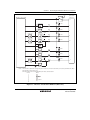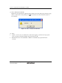
1
To our customers,
Old Company Name in Catalogs and Other Documents
On April 1st, 2010, NEC Electronics Corporation merged with Renesas Technology
Corporation, and Renesas Electronics Corporation took over all the business of both
companies. Therefore, although the old company name remains in this document, it is a valid
Renesas Electronics document. We appreciate your understanding.
Renesas Electronics website: http://www.renesas.com
April 1st, 2010
Renesas Electronics Corporation
Issued by: Renesas Electronics Corporation (http://www.renesas.com)
Send any inquiries to http://www.renesas.com/inquiry.
Notice
1.
2.
3.
4.
5.
6.
7.
All information included in this document is current as of the date this document is issued. Such information, however, is
subject to change without any prior notice. Before purchasing or using any Renesas Electronics products listed herein, please
confirm the latest product information with a Renesas Electronics sales office. Also, please pay regular and careful attention to
additional and different information to be disclosed by Renesas Electronics such as that disclosed through our website.
Renesas Electronics does not assume any liability for infringement of patents, copyrights, or other intellectual property rights
of third parties by or arising from the use of Renesas Electronics products or technical information described in this document.
No license, express, implied or otherwise, is granted hereby under any patents, copyrights or other intellectual property rights
of Renesas Electronics or others.
You should not alter, modify, copy, or otherwise misappropriate any Renesas Electronics product, whether in whole or in part.
Descriptions of circuits, software and other related information in this document are provided only to illustrate the operation of
semiconductor products and application examples. You are fully responsible for the incorporation of these circuits, software,
and information in the design of your equipment. Renesas Electronics assumes no responsibility for any losses incurred by
you or third parties arising from the use of these circuits, software, or information.
When exporting the products or technology described in this document, you should comply with the applicable export control
laws and regulations and follow the procedures required by such laws and regulations. You should not use Renesas
Electronics products or the technology described in this document for any purpose relating to military applications or use by
the military, including but not limited to the development of weapons of mass destruction. Renesas Electronics products and
technology may not be used for or incorporated into any products or systems whose manufacture, use, or sale is prohibited
under any applicable domestic or foreign laws or regulations.
Renesas Electronics has used reasonable care in preparing the information included in this document, but Renesas Electronics
does not warrant that such information is error free. Renesas Electronics assumes no liability whatsoever for any damages
incurred by you resulting from errors in or omissions from the information included herein.
Renesas Electronics products are classified according to the following three quality grades: “Standard”, “High Quality”, and
“Specific”. The recommended applications for each Renesas Electronics product depends on the product’s quality grade, as
indicated below. You must check the quality grade of each Renesas Electronics product before using it in a particular
application. You may not use any Renesas Electronics product for any application categorized as “Specific” without the prior
written consent of Renesas Electronics. Further, you may not use any Renesas Electronics product for any application for
which it is not intended without the prior written consent of Renesas Electronics. Renesas Electronics shall not be in any way
liable for any damages or losses incurred by you or third parties arising from the use of any Renesas Electronics product for an
application categorized as “Specific” or for which the product is not intended where you have failed to obtain the prior written
consent of Renesas Electronics. The quality grade of each Renesas Electronics product is “Standard” unless otherwise
expressly specified in a Renesas Electronics data sheets or data books, etc.
“Standard”:
8.
9.
10.
11.
12.
Computers; office equipment; communications equipment; test and measurement equipment; audio and visual
equipment; home electronic appliances; machine tools; personal electronic equipment; and industrial robots.
“High Quality”: Transportation equipment (automobiles, trains, ships, etc.); traffic control systems; anti-disaster systems; anticrime systems; safety equipment; and medical equipment not specifically designed for life support.
“Specific”:
Aircraft; aerospace equipment; submersible repeaters; nuclear reactor control systems; medical equipment or
systems for life support (e.g. artificial life support devices or systems), surgical implantations, or healthcare
intervention (e.g. excision, etc.), and any other applications or purposes that pose a direct threat to human life.
You should use the Renesas Electronics products described in this document within the range specified by Renesas Electronics,
especially with respect to the maximum rating, operating supply voltage range, movement power voltage range, heat radiation
characteristics, installation and other product characteristics. Renesas Electronics shall have no liability for malfunctions or
damages arising out of the use of Renesas Electronics products beyond such specified ranges.
Although Renesas Electronics endeavors to improve the quality and reliability of its products, semiconductor products have
specific characteristics such as the occurrence of failure at a certain rate and malfunctions under certain use conditions. Further,
Renesas Electronics products are not subject to radiation resistance design. Please be sure to implement safety measures to
guard them against the possibility of physical injury, and injury or damage caused by fire in the event of the failure of a
Renesas Electronics product, such as safety design for hardware and software including but not limited to redundancy, fire
control and malfunction prevention, appropriate treatment for aging degradation or any other appropriate measures. Because
the evaluation of microcomputer software alone is very difficult, please evaluate the safety of the final products or system
manufactured by you.
Please contact a Renesas Electronics sales office for details as to environmental matters such as the environmental
compatibility of each Renesas Electronics product. Please use Renesas Electronics products in compliance with all applicable
laws and regulations that regulate the inclusion or use of controlled substances, including without limitation, the EU RoHS
Directive. Renesas Electronics assumes no liability for damages or losses occurring as a result of your noncompliance with
applicable laws and regulations.
This document may not be reproduced or duplicated, in any form, in whole or in part, without prior written consent of Renesas
Electronics.
Please contact a Renesas Electronics sales office if you have any questions regarding the information contained in this
document or Renesas Electronics products, or if you have any other inquiries.
(Note 1) “Renesas Electronics” as used in this document means Renesas Electronics Corporation and also includes its majorityowned subsidiaries.
(Note 2) “Renesas Electronics product(s)” means any product developed or manufactured by or for Renesas Electronics.
User’s Manual
H8S, H8SX Family E10A-USB
Emulator
Additional Document for User’s Manual
Supplementary Information on Using
the H8SX/1651
Renesas Microcomputer Development
Environment System
H8SX Family / H8SX/1600 Series
E10A-USB for H8SX/1651 HS1651KCU01HE
Rev.5.00 2009.07
Rev. 5.00 Jul. 31, 2009 Page ii of vi
REJ10J1283-0500
Notes regarding these materials
1. This document is provided for reference purposes only so that Renesas customers may select the appropriate
Renesas products for their use. Renesas neither makes warranties or representations with respect to the
accuracy or completeness of the information contained in this document nor grants any license to any
intellectual property rights or any other rights of Renesas or any third party with respect to the information in
this document.
2. Renesas shall have no liability for damages or infringement of any intellectual property or other rights arising
out of the use of any information in this document, including, but not limited to, product data, diagrams, charts,
programs, algorithms, and application circuit examples.
3. You should not use the products or the technology described in this document for the purpose of military
applications such as the development of weapons of mass destruction or for the purpose of any other military
use. When exporting the products or technology described herein, you should follow the applicable export
control laws and regulations, and procedures required by such laws and regulations.
4. All information included in this document such as product data, diagrams, charts, programs, algorithms, and
application circuit examples, is current as of the date this document is issued. Such information, however, is
subject to change without any prior notice. Before purchasing or using any Renesas products listed in this
document, please confirm the latest product information with a Renesas sales office. Also, please pay regular
and careful attention to additional and different information to be disclosed by Renesas such as that disclosed
through our website. (http://www.renesas.com )
5. Renesas has used reasonable care in compiling the information included in this document, but Renesas
assumes no liability whatsoever for any damages incurred as a result of errors or omissions in the information
included in this document.
6. When using or otherwise relying on the information in this document, you should evaluate the information in
light of the total system before deciding about the applicability of such information to the intended application.
Renesas makes no representations, warranties or guaranties regarding the suitability of its products for any
particular application and specifically disclaims any liability arising out of the application and use of the
information in this document or Renesas products.
7. With the exception of products specified by Renesas as suitable for automobile applications, Renesas
products are not designed, manufactured or tested for applications or otherwise in systems the failure or
malfunction of which may cause a direct threat to human life or create a risk of human injury or which require
especially high quality and reliability such as safety systems, or equipment or systems for transportation and
traffic, healthcare, combustion control, aerospace and aeronautics, nuclear power, or undersea communication
transmission. If you are considering the use of our products for such purposes, please contact a Renesas
sales office beforehand. Renesas shall have no liability for damages arising out of the uses set forth above.
8. Notwithstanding the preceding paragraph, you should not use Renesas products for the purposes listed below:
(1) artificial life support devices or systems
(2) surgical implantations
(3) healthcare intervention (e.g., excision, administration of medication, etc.)
(4) any other purposes that pose a direct threat to human life
Renesas shall have no liability for damages arising out of the uses set forth in the above and purchasers who
elect to use Renesas products in any of the foregoing applications shall indemnify and hold harmless Renesas
Technology Corp., its affiliated companies and their officers, directors, and employees against any and all
damages arising out of such applications.
9. You should use the products described herein within the range specified by Renesas, especially with respect
to the maximum rating, operating supply voltage range, movement power voltage range, heat radiation
characteristics, installation and other product characteristics. Renesas shall have no liability for malfunctions or
damages arising out of the use of Renesas products beyond such specified ranges.
10. Although Renesas endeavors to improve the quality and reliability of its products, IC products have specific
characteristics such as the occurrence of failure at a certain rate and malfunctions under certain use
conditions. Please be sure to implement safety measures to guard against the possibility of physical injury, and
injury or damage caused by fire in the event of the failure of a Renesas product, such as safety design for
hardware and software including but not limited to redundancy, fire control and malfunction prevention,
appropriate treatment for aging degradation or any other applicable measures. Among others, since the
evaluation of microcomputer software alone is very difficult, please evaluate the safety of the final products or
system manufactured by you.
11. In case Renesas products listed in this document are detached from the products to which the Renesas
products are attached or affixed, the risk of accident such as swallowing by infants and small children is very
high. You should implement safety measures so that Renesas products may not be easily detached from your
products. Renesas shall have no liability for damages arising out of such detachment.
12. This document may not be reproduced or duplicated, in any form, in whole or in part, without prior written
approval from Renesas.
13. Please contact a Renesas sales office if you have any questions regarding the information contained in this
document, Renesas semiconductor products, or if you have any other inquiries.
Rev. 5.00 Jul. 31, 2009 Page iii of vi
REJ10J1283-0500
Rev. 5.00 Jul. 31, 2009 Page iv of vi
REJ10J1283-0500
Contents
Section 1 Connecting the Emulator with the User System................................1
1.1
1.2
1.3
1.4
Components of the E10A-USB Emulator ......................................................................... 1
Connecting the E10A-USB Emulator with the User System ............................................ 3
Pin Assignments of the E10A-USB Connector ................................................................ 5
Example of Emulator Connection..................................................................................... 6
Section 2 Specification of the Emulator’s Software..........................................11
2.1
2.2
Differences between the H8SX/1651 and the Emulator ................................................... 11
The H8SX/1651 E10A-USB Emulator Specific Functions and Notes ............................. 13
2.2.1 Emulator Driver Selection ................................................................................... 13
2.2.2 Hardware Break Functions .................................................................................. 13
2.2.3 Notes on Setting the [Breakpoint] Dialog Box .................................................... 15
2.2.4 Sequential Break Function................................................................................... 16
2.2.5 Note on Using the JTAG Clock (TCK) ............................................................... 16
2.2.6 Trace Function ..................................................................................................... 16
2.2.7 Parallel Transfer................................................................................................... 17
2.2.8 Debugging in the External Flash Memory........................................................... 20
2.2.9 Interface with Initialization, Write, and Erase Modules and Emulator
Firmware.............................................................................................................. 24
2.2.10 Tutorial ................................................................................................................ 25
2.2.11 Performance Analysis .......................................................................................... 26
Rev. 5.00 Jul. 31, 2009 Page v of vi
REJ10J1283-0500
Rev. 5.00 Jul. 31, 2009 Page vi of vi
REJ10J1283-0500
Section 1 Connecting the Emulator with the User System
Section 1 Connecting the Emulator with the User System
1.1
Components of the E10A-USB Emulator
The H8SX/1651 E10A-USB emulator supports the H8SX/1651 (hereafter referred to as the MCU
unless the description is specific to it). Table 1.1 lists the components of the H8SX/1651 E10AUSB emulator.
Rev. 5.00 Jul. 31, 2009 Page 1 of 30
REJ10J1283-0500
Section 1 Connecting the Emulator with the User System
Table 1.1 Components of the Emulator
Classification Component
Hardware
Emulator box
Appearance
Quantity
1
Remarks
HS0005KCU01H:
Depth: 65.0 mm, Width: 97.0 mm,
Height: 20.0 mm, Mass: 72.9 g
or
*1
HS0005KCU02H :
Depth: 65.0 mm, Width: 97.0 mm,
Height: 20.0 mm, Mass: 73.7 g
Software
User system interface
cable
1
14-pin type:
Length: 20 cm, Mass: 33.1 g
USB cable
1
Length: 150 cm, Mass: 50.6 g
H8SX/1651 E10A-USB
emulator setup program,
H8S, H8SX Family
E10A-USB Emulator
User’s Manual,
Supplementary
Information on Using the
*2
H8SX/1651 , and
Test program manual for
HS0005KCU01H and
HS0005KCU02H
1
HS0005KCU01SR,
HS0005KCU01HJ-H8S,
HS0005KCU01HE-H8S,
HS1651KCU01HJ,
HS1651KCU01HE,
HS0005TM01HJ, and
HS0005TM01HE
(provided on a CD-R)
Notes: 1. When HS0005KCU02H is purchased, the 36-pin type cable is provided; however, it is
not available for this MCU.
2. Additional document for the MCUs supported by the emulator is included. Check the
target MCU and refer to its additional document.
Rev. 5.00 Jul. 31, 2009 Page 2 of 30
REJ10J1283-0500
Section 1 Connecting the Emulator with the User System
1.2
Connecting the E10A-USB Emulator with the User System
Before connecting an E10A-USB emulator (hereafter referred to as the emulator) with the user
system, a connector must be installed in the user system so that a user system interface cable can
be connected. When designing the user system, refer to the connector and recommended circuits
shown in this manual.
Before designing the user system, be sure to read the H8S, H8SX Family E10A-USB Emulator
User’s Manual and the hardware manual for related MCUs.
Connect pins 8, 9, 10, 12, 13, and 14 of the user system connector to GND firmly on the PCB.
These pins are used as electrical GND and to monitor the connection of the user system connector.
Note the pin assignments of the user system connector.
User system interface cable
Tab
GND line
User system connector
Pin 8
User system GND
connection
Pin 1
User system
Figure 1.1 Connecting the User System Interface Cable to the User System
Notes: 1. The pin number assignments of the 14-pin connector differ from those of the E8
emulator; however, the physical location is the same.
2. Do not place any components within 3 mm of the connector.
Rev. 5.00 Jul. 31, 2009 Page 3 of 30
REJ10J1283-0500
Section 1 Connecting the Emulator with the User System
WARNING
Be sure to place the GND line of the user system interface
cable on the GND of the user system with a screw, etc. Failure
to do so will result in a FIRE HAZARD due to an overcurrent
and will damage the user system, the emulator product, and
the host computer.
Rev. 5.00 Jul. 31, 2009 Page 4 of 30
REJ10J1283-0500
Section 1 Connecting the Emulator with the User System
1.3
Pin Assignments of the E10A-USB Connector
Figure 1.2 shows the pin assignments of the user system connector.
Pin No.
Pin 1 mark
User system connector
Pin 14
Pin 7
Pin 8
Pin 1
MCU Pin Name
Input/Output *1
1
P65
Input
2
P62
Input
3
WDTOVF#
Output
4
RES(in)# *2 *5
Input
5
P63
Input
6
P64
Input
7
RES(out)# *2
Output
8 to 10
GND *3
12 to 14
11
Vcc *4
Top view
Pin 1 mark
Notes: 1. Input to or output from the user system.
2. The symbol (#) means that the signal is active-low.
3. By detecting GND on the user system, the emulator decides
whether the user system is connected or not.
4. Connect Vcc with the Vcc of the MCU.
5. RES(in) is not the pin name of the MCU. It cannot be directly
connected to the MCU pins.
Figure 1.2 Pin Assignments of the User System Connector
Rev. 5.00 Jul. 31, 2009 Page 5 of 30
REJ10J1283-0500
Section 1 Connecting the Emulator with the User System
1.4
Example of Emulator Connection
The figure shown below is an example of connecting the user system to the emulator.
14-pin connector with
a 2.54-mm pitch
(3M Limited: 2514-6002)
Pulled up at 4.7 kΩ
Vcc
MCU
11
EMLE
1
P65
2
P62
3
WDTOVF#
5
P63
6
P64
4
User logic
7
RES#
8 to 10
12 to 14
E10A-USB pin no.
User system
· RES(in)# of pin 4 of the user system connector is a signal line in which the emulator outputs signals to the MCU.
RES(in)# (pin 4) and the user logic reset circuit for the signal line must be connected to the MCU as shown above.
· RES(out)# of pin 7 of the user system connector is a signal line in which the emulator monitors the RES# signal of
the MCU. The RES# must be pulled up before it is connected to pin 7 of the user system connector.
Figure 1.3 Example of Emulator Connection
Rev. 5.00 Jul. 31, 2009 Page 6 of 30
REJ10J1283-0500
Section 1 Connecting the Emulator with the User System
Notes: 1. P62, P65, P63, WDTOVF#, and P64 are used by the emulator. Pull up and connect the
emulator and the MCU pins.
MCU
User system
connector
Vcc
4.7 kΩ
Pins 1, 2, 3, 5, and 6
Figure 1.4 Connection of Emulator and MCU
2.
If the emulator is connected to the user system, pull up pin EMLE of the MCU, and
when the emulator is not connected to the user system, ground the EMLE.
MCU
Vcc
The emulator is connected
to the user system.
4.7 k
EMLE
MCU
The emulator is not connected
to the user system.
EMLE
Figure 1.5 Emulator and Pin EMLE
Rev. 5.00 Jul. 31, 2009 Page 7 of 30
REJ10J1283-0500
Section 1 Connecting the Emulator with the User System
3.
RES(in)# of pin 4 of the user system connector is a signal line in which the emulator
outputs signals to the MCU. RES(in)# of pin 4 and the user logic reset circuit for the
signal line must be connected to pin RES# of the MCU as shown in figure 1.6.
RES(out)# of pin 7 of the user system connector is a signal line in which the emulator
monitors pin RES# of the MCU.
The RES# must be pulled up before it is connected to pin 7 of the user system
connector.
Vcc
4.7 kΩ
User system
connector
User
logic
MCU
Vcc
RES(in)# (pin 4)
4.7 kΩ
RES#
RES(out)# (pin 7)
Figure 1.6 Connection of Pin RES#
4.
Ground pins 8, 9, 10, 12, 13, and 14 of the user system connector.
5.
Pin 11 of the user system connector must be connected to the user system Vcc (power
supply). The amount of voltage permitted to input to the user system connector must
be within the guaranteed range of the MCU.
6.
Figure 1.7 shows the interface circuit in the emulator. Use this figure as a reference to
decide the pull-up resistance value.
Rev. 5.00 Jul. 31, 2009 Page 8 of 30
REJ10J1283-0500
Section 1 Connecting the Emulator with the User System
SW2
3.3 V
0
Emulator control circuit
1
User system
connector *3
11
SN74LVC2G125
VCC
22 Ω
A
10 kΩ
1
Y
SN74LVC2G125
VCC
22 Ω
A
PI74AVC164245
SN74LVC2G125
A
PI74AVC164245
Y
22 Ω
A
10 kΩ
3
A
SN74LVC2G125
1.8 V
22 Ω
VCC
B
2
1.8 V
VCC
B
10 kΩ
Y
Y
10 kΩ
4 *1
A
SN74LVC2G125
VCC
A
Y
SN74LVC2G125
VCC
22 Ω
A
10 kΩ
5
Y
SN74LVC2G125
VCC
A
PI74AVC164245
22 Ω
SN74LVC2G125
VCC
B
A
Y
10 kΩ
6
Y
1.8 V
22 Ω
10 kΩ
7 *2
A
SN74LVC2G125
VCC
OE
A
Y
Notes: 1. The emulator outputs the reset signal to pin 4. Therefore, pin 4 cannot be directly connected to pin RES# of the MCU.
2. The emulator only monitors pin 7.
3. The pin numbers and corresponding MCU pin names are listed below.
Pin No.
1
2
3
4
5
6
7
11
MCU
P65
P62
WDTOVF#
RES(in)# *1
P63
P64
RES(out)# *2
Vcc
Figure 1.7 Interface Circuit in the Emulator (Reference)
Rev. 5.00 Jul. 31, 2009 Page 9 of 30
REJ10J1283-0500
Section 1 Connecting the Emulator with the User System
7.
When the MCU in use is connected to the emulator, the pin functions listed below are
not available.
Table 1.2 Pin Functions Not Available
H8SX/1651
WDTOVF# and P62 to P65
TMO3, TMCI3, TMRI3, and TMO2
IRQ10#-B and IRQ11#-B
DACK2#, DREQ3#, TEND3#, and DACK3#
SCK4
The symbol (#) means that the signal is active-low.
Rev. 5.00 Jul. 31, 2009 Page 10 of 30
REJ10J1283-0500
Section 2 Specification of the Emulator’s Software
Section 2 Specification of the Emulator’s Software
2.1
Differences between the H8SX/1651 and the Emulator
1. When the emulator system is initiated, it initializes the general registers and part of the control
registers as shown in table 2.1. The initial value of the MCU is undefined. When the emulator
is initiated from the workspace, a value to be entered is saved in a session.
For the registers shown in table 2.1, values other than PC or CCR are not changed even if the
CPU reset command is issued. If ER7 (SP) is changed as an odd value, it must be modified in
the [Register] window.
Table 2.1 Register Initial Values at Emulator Power-On
Register
Initial Value
PC
Reset vector value in the vector address table
ER0 to ER6
H’0
ER7 (SP)
H'10
CCR
1 for I mask, and others undefined
EXR
H’7F
VBR
H’0
SBR
H’FFFFFF00
MACH
H’0
MACL
H’0
2. System Control Register
In the emulator, the internal I/O registers can be accessed from the [IO] window. However, be
careful when accessing the system control register. The emulator saves the register value of
the system control register at a break and returns the value when the user program is executed.
Since this is done during a break, do not rewrite the system control register in the [IO]
window.
3. Memory Access during Emulation
If the memory contents are referenced or modified during emulation, realtime emulation
cannot be performed because the user program is temporarily halted.
4. The emulator communicates with the MCU by using the pins shown in figure 1.2 in section
1.3. These pins cannot be used.
Rev. 5.00 Jul. 31, 2009 Page 11 of 30
REJ10J1283-0500
Section 2 Specification of the Emulator’s Software
5. The power consumed by the MCU can reach several mA. This is because the user power
supply drives ICs to make the communication signal level match the user-system powersupply voltage.
6. MCU Operating Mode
Use the emulator in mode 4 or mode 5.
Rev. 5.00 Jul. 31, 2009 Page 12 of 30
REJ10J1283-0500
Section 2 Specification of the Emulator’s Software
2.2
The H8SX/1651 E10A-USB Emulator Specific Functions and Notes
2.2.1
Emulator Driver Selection
Table 2.2 shows drivers which can be selected in the [Driver Details] dialog box.
Table 2.2 Type Name and Driver
Type Name
Driver
HS0005KCU01H, HS0005KCU02H
Renesas E-Series USB Driver
2.2.2
Hardware Break Functions
Hardware Break Conditions: In the H8SX/1651 E10A-USB emulator, conditions of Break
Condition 1,2,3,4 can be set. Table 2.3 lists the items that can be specified.
Table 2.3 Hardware Break Condition Specification Items
Items
Description
Address bus condition
Breaks when the MCU address bus value matches the
specified value. It is possible to select whether a break is
generated before or after prefetched address execution.
When [User mask] is selected, a value to be masked ‘*’ can
be set. For masked bits, the condition is satisfied for any
values.
Data bus condition
Breaks when the MCU data bus value matches the specified
value. Byte, word, or longword can be specified as the
access data size.
When [User mask] is selected, a value to be masked ‘*’ can
be set. For masked bits, the condition is satisfied for any
values.
Bus master condition
Breaks when the values of DATA, DTC, and DMA cycles
match the specified values.
Read or write condition
Breaks in the read or write cycle.
Execution count condition
The condition specified with Break Condition 1 breaks after
the execution count condition specified here has been
satisfied.
Rev. 5.00 Jul. 31, 2009 Page 13 of 30
REJ10J1283-0500
Section 2 Specification of the Emulator’s Software
Table 2.4 lists the combinations of conditions that can be set in the [Break condition] dialog box.
Table 2.4 Conditions Set in [Break condition] Dialog Box
Condition
Dialog Box
[Break condition 1]
[Break condition 2]
[Break condition 3]
[Break condition 4]
Address Bus Data
Condition
Condition
O
O
O
O
O
X
X
X
Bus Master
Condition
Execution
Read or Write Count
Condition
Condition
O
O
O
O
O
O
O
O
O
X
X
X
Note: O: Can be set by checking the radio button in the dialog box.
Table 2.5 lists the combinations of conditions that can be set by the BREAKCONDITION_SET
command.
Table 2.5 Conditions Set by BREAKCONDITION_SET Command
Condition
Channel
Break condition 1
Break condition 2
Break condition 3
Break condition 4
Address Bus
Condition
(option
<addropt>)
O
O
O
O
Data
Condition
(option
<dataopt>)
O
X
X
X
Bus Master
Condition
(option
<accessopt>)
Read or Write
Condition
(option
<r/wopt>)
O
O
O
O
O
O
O
O
Note: O: Can be set by the BREAKCONDITION_SET command.
Rev. 5.00 Jul. 31, 2009 Page 14 of 30
REJ10J1283-0500
Execution
Count
Condition
(option
<countopt>)
O
X
X
X
Section 2 Specification of the Emulator’s Software
Notes on Setting the Break Condition:
1. When [Step In], [Step Over], or [Step Out] is selected, the settings of Break Condition are
disabled.
2. The settings of Break Condition are disabled when an instruction to which a BREAKPOINT
has been set is executed.
3. When step over function is used, the settings of BREAKPOINT and Break Condition are
disabled.
4. When [Go To Cursor] is selected, the settings of Break Condition channel 4 are disabled.
2.2.3
Notes on Setting the [Breakpoint] Dialog Box
1. When an odd address is set, the address is rounded down to an even address.
2. A BREAKPOINT is accomplished by replacing instructions. Accordingly, it can be set only
to the flash RAM area. An external flash memory must be enabled referring to section 2.2.7,
Debugging in the External Flash Memory, to set a BREAKPOINT in the external flash
memory. However, a BREAKPOINT cannot be set to the following addresses:
• An area other than flash RAM
• An area occupied by the emulator program
3. During step execution, a BREAKPOINT is disabled.
4. A condition set at Break Condition is disabled immediately after starting execution when an
instruction at a BREAKPOINT is executed. A break does not occur even if a condition of
Break Condition is satisfied immediately after starting the execution.
5. When execution resumes from the breakpoint address after the program execution stops at the
BREAKPOINT, single-step execution is performed at the address before execution resumes.
Therefore, realtime operation cannot be performed.
6. Settings of BREAKPOINT and Break Condition are invalid while the STEP OVER function is
being used.
7. When a BREAKPOINT is set in the external flash memory area, the emulator executes the
programs for initializing, programming, and erasing the flash memory (hereafter referred to as
an initialization module, a write module, and an erase module, respectively*) to reprogram the
external flash memory. Accordingly, the operation of the user program will differ when it is
reexecuted after a break occurs.
Note: Prepare initialization, write, and erase modules that are suitable for the external flash
memory being used.
Rev. 5.00 Jul. 31, 2009 Page 15 of 30
REJ10J1283-0500
Section 2 Specification of the Emulator’s Software
2.2.4
Sequential Break Function
The user program is halted when conditions of the Break Condition for channels 2 to 4 are
matched. This function can be set in the [Emulation mode] drop-down list box of the
[Configuration] dialog box.
Table 2.6 Sequential Break Condition Specification Items
Items
Description
Sequential break Condition 2-1
Halts a program when a condition is satisfied in the order of
Break Condition 2, 1.
Break Condition 1, 2 must be set.
Sequential break Condition 3-2-1
Halts a program when a condition is satisfied in the order of
Break Condition 3, 2, 1.
Break Condition 1, 2, 3 must be set.
Sequential break Condition 4-3-2-1
Halts a program when a condition is satisfied in the order of
Break Condition 4, 3, 2, 1.
Break Condition 1, 2, 3, 4 must be set.
Note: When Sequential break Condition 4-3-2-1 is set, [Go To Cursor] is not available.
2.2.5
Note on Using the JTAG Clock (TCK)
When the JTAG clock (TCK) is used, set the frequency to lower than that of the system clock.
2.2.6
Trace Function
The emulator uses the eight-branch-instruction trace function in the MCU, and acquires a trace by
operating the user program in realtime. The branch-instruction trace function displays the branchsource address, the mnemonic, and the operand.
Rev. 5.00 Jul. 31, 2009 Page 16 of 30
REJ10J1283-0500
Section 2 Specification of the Emulator’s Software
2.2.7
Parallel Transfer
(1) This emulator supports memory accesses during user program execution using a DTC parallel
transfer. To enable the DTC parallel transfer, select [Enable] for [Parallel] in the
[Configuration] dialog box.
Figure 2.1 [Configuration] Dialog Box
[Parallel] group box:
Selects the setting on memory accesses during user program
execution.
Table 2.7 [Parallel] Group Box
Disable
Uses no emulator debugging function (DTC parallel transfer) to access memory.
A short break occurs. (initial value)
Enable
Uses the emulator debugging function (DTC parallel transfer) to access memory.
Rev. 5.00 Jul. 31, 2009 Page 17 of 30
REJ10J1283-0500
Section 2 Specification of the Emulator’s Software
(2) Limitations on DTC Parallel Transfer Enabled
⎯ If the reserved area is accessed during DTC parallel transfer, a DMA address error occurs.
Be sure to set the interrupt exception processing for the CPU or DMA address error on the
user program.
⎯ Use of DTC parallel transfer to access memory is prohibited in software standby mode;
H’FF is displayed. If the emulator enters the software standby mode during DTC parallel
transfer, correct transfer will not be performed. When the DTC parallel transfer function is
used again, reconnect the emulator.
⎯ If the DTC parallel transfer function is used to access I/O registers (I/O areas), accessing
memory is prohibited in the range H’FFFF00 to H’FFFF1F (H’FF is displayed).
⎯ If the user program is halted by a breakpoint or a Break condition during DTC parallel
transfer, correct transfer will not be performed and a dialog box will be displayed. When
the DTC parallel transfer function is used again, reconnect the emulator.
⎯ For reserved or external areas, accessing memory is available when external areas are set.
H’FF is displayed only when reserved areas are set.
Rev. 5.00 Jul. 31, 2009 Page 18 of 30
REJ10J1283-0500
Section 2 Specification of the Emulator’s Software
Figure 2.2 shows if an access to each area is possible or not during user program execution.
Figure 2.2 Parallel Accesses in Various Memory Areas
Rev. 5.00 Jul. 31, 2009 Page 19 of 30
REJ10J1283-0500
Section 2 Specification of the Emulator’s Software
2.2.8
Debugging in the External Flash Memory
This emulator supports debugging in the external flash memory, which is the function to allow
downloading of programs to the external flash memory area. Settings for the external flash
memory should be made in the [External Flash memory setting] dialog box opened at initiation of
the emulator. To display the [External Flash memory setting] dialog box, check [Use External
Flash memory setting] in the [Select Emulator mode] dialog box. Debugging function equivalent
to that in the H8SX E10A-USB system becomes available in the external flash memory area by
specifying the initialization, write, or erase module* and filling information on the external flash
memory. Settings made in the [External Flash memory setting] dialog box are retained. Next time
this dialog box is launched, the previous settings are displayed. Clicking the [Save] button saves
the contents that have been set. The file to be saved (*.EFF: external flash memory data setting
file) is loaded by clicking the [Browse…] button for [Select External Flash setting file]. When the
file has been set, it is registered as the history (recent 10 files) in the combo box and selected to be
loaded. Up to 1024 blocks can be specified for the external flash memory via the [External Flash
memory setting] dialog box of the emulator. The maximum size allowed between the start address
and the end address of the external flash memory is 16 Mbytes. Since this function forcibly
changes the device settings in the emulator when the initialization, write, or erase module is
called, the emulator operates differently with the contents of the user program. To verify the
operation of the user program, disable the [Use External Flash memory] check box and activate
the emulator.
Notes: 1. Prepare initialization, write, and erase modules that are suitable for the external flash
memory being used.
2. Make settings in accord with the region of memory on the individual device.
Table 2.8 lists the items contained in the [External Flash memory setting] dialog box.
Rev. 5.00 Jul. 31, 2009 Page 20 of 30
REJ10J1283-0500
Section 2 Specification of the Emulator’s Software
Figure 2.3 [External Flash memory setting] Dialog Box
Rev. 5.00 Jul. 31, 2009 Page 21 of 30
REJ10J1283-0500
Section 2 Specification of the Emulator’s Software
Table 2.8 Items in [External Flash memory setting] Dialog Box
No.
Item
Description
1
Select External Flash setting
file
Specify the data file (*.EFF) for setting the external flash
memory. If not specified, select the setting of [recent
setting data] (data previously changed) in the combo box.
To make a new setting, select [initialize] and input data.
2
Use External Flash memory
Enable or disable use of the external flash memory
debugging function.
Checked: Enabled
Not checked: Disabled (default)
3
Erasing External Flash
memory at Link up
Select whether or not to erase the contents of the flash
memory at initiation of the emulator.
Checked: Erases the contents of the flash memory at
initiation of the emulator.
Not checked: Reads the contents of the flash memory at
initiation of the emulator (default).
4
File name
Specify the file of initialization, write, and erase modules. A
program file must be specified for programming the flash
memory. Prepare a file suitable for the flash memory being
used.
5
Module offset address
Specify the top address by an offset where the initialization,
write, erasing modules are to be expanded. (Initial value is
H’0). If not specified, disable offset.
Checked: Enables offset.
Not checked: Disables offset (default).
(If the address exceeds H’FFFFFFFF, it will become H’0.)
6
Module top address
Specify the start address where the initialization, write, and
erase modules are to be expanded. (The 4-kbyte address
areas starting from that address are saved by the emulator;
it is possible to expand the initialization, write, and erase
modules without affecting on the user program.)
7
Initialize module address
Entry address of the initialization module
The initialization module is used to set the device that is
required for accessing the external flash memory. If not
specified, disable entry.
Checked: Enables entry.
Not checked: Disables entry (default).
8
Erasing module address
Rev. 5.00 Jul. 31, 2009 Page 22 of 30
REJ10J1283-0500
Entry address of the erase module
Section 2 Specification of the Emulator’s Software
Table 2.8 Items in [External Flash memory setting] Dialog Box (cont)
No.
Item
Description
9
Writing module address
Entry address of the write module
10
Access size
Select the unit of accesses for transfer of the programs.
8bits(Byte): Bytes
16bits(Word): Words
32bits(Long): Longwords
11
Top address
Start address of the flash memory
12
End address
End address of the flash memory*
13
Bus width
Select the unit of accesses to the flash memory.
8bits(Byte): Bytes
16bits(Word): Words
32bits(Long): Longwords
14
Erasing time
Waiting time for erasure (in seconds)
(Specification of a decimal or hexadecimal value is
recommended.)
15
Block count
Number of blocks in the flash memory
(Specification of a decimal or hexadecimal value is
recommended. Up to 1024 blocks can be specified.)
16
Top address of block
Define the start addresses of all blocks. If the flash
memory has D’10 blocks, the definition will be as shown
below. Press the Return key between the definitions for
each of the blocks.
Example:
H’0
H’1000
H’2000
H’3000
H’4000
H’5000
H’6000
H’7000
H’8000
H’9000
17
Remarks
Use for writing a text. Contents of data that has been set
can be entered. If not specified, setting is not needed.
Note: Make settings in accord with the region of memory on the individual device.
Rev. 5.00 Jul. 31, 2009 Page 23 of 30
REJ10J1283-0500
Section 2 Specification of the Emulator’s Software
2.2.9
Interface with Initialization, Write, and Erase Modules and Emulator Firmware
The initialization, write, and erase modules must be branched from the firmware when the
emulator is initiated and the external flash memory is written or read*.
Note: The modules are not called if the external flash memory data is not updated.
To branch from the emulator firmware to the initialization, write, and erase modules, or to return
from the initialization, write, and erase modules to the emulator firmware, the following
conditions must be observed:
• The size of each initialization, write, or erase module must be consecutive 4 kbytes or less
(including work areas and stack areas).
• Save and return all the general register values and control register values before and after
calling the initialization, write, or erase module.
• Return the initialization, write, or erase module to the calling source after processing.
• The initialization, write, and erase modules must be Motorola S-type files.
• For the write module, write data ER1(L) to address ER0(L) and store the top address of flash
memory ER2(L) then the result in ER0(L).
• For the erase module, erase the block of address ER0(L) and store the top address of flash
memory ER1(L) then the result in ER0(L).
• Set the write size of the write module as described in No. 13 ‘Bus width’ in table 2.8 (byte,
word, or longword).
• The initialization module is used to set the device that is required for accessing the external
flash memory. Store the result in ER0(L).
The module interface must be as follows to correctly pass the information that is required for
accessing flash memory.
Rev. 5.00 Jul. 31, 2009 Page 24 of 30
REJ10J1283-0500
Section 2 Specification of the Emulator’s Software
Table 2.9 Module Interface
Module Name
Argument
Return Value
Write module
ER0(L): Write address
ER0(L): Result (OK = 0, NG ≠ 0)
ER1(L): Write data
ER2(L): Top address of the
flash memory
Erase module
ER0(L): Address of the block
to be erased
ER0(L): Result (OK = 0, NG ≠ 0)
ER1(L): Top address of the
flash memory
Initialization module
-
ER0(L): Result (OK = 0, NG ≠ 0)
Notes: 1. The (L) means the longword size.
2. The initialization module is not always set.
2.2.10
Tutorial
This product does not contain tutorial.
Rev. 5.00 Jul. 31, 2009 Page 25 of 30
REJ10J1283-0500
Section 2 Specification of the Emulator’s Software
2.2.11
(1)
Performance Analysis
Measuring Performance
Use the performance analysis function to measure the performance of programs. The
performance analysis function does not affect the realtime operation because it uses an on-chip
performance-measurement circuit to measure the performance in a specified range.
To open the [Performance Analysis] window, start by selecting [View -> Performance ->
Performance Analysis] or clicking on the [PA] toolbar button ( ). The [Select Performance
Analysis Type] dialog box appears.
Figure 2.4 [Select Performance Analysis Type] Dialog Box
Click on the [OK] button to open the [Performance Analysis] window.
Figure 2.5 [Performance Analysis] Window
Performance-measurement settings should be made in the [Performance Analysis] dialog box.
Rev. 5.00 Jul. 31, 2009 Page 26 of 30
REJ10J1283-0500
Section 2 Specification of the Emulator’s Software
Figure 2.6 [Performance Analysis] Dialog Box
The [Performance Analysis] dialog box contains the following items.
[Channel 1] group box: Settings on PA1
[Don’t care] checkbox
Selected:
Performance measurement will not be performed on PA1.
Not selected:
Performance measurement will be performed on PA1.
PA1 is for measuring the number of execution cycles in the
entire program.
Rev. 5.00 Jul. 31, 2009 Page 27 of 30
REJ10J1283-0500
Section 2 Specification of the Emulator’s Software
[Channel 2] group box: Settings on PA2
[Don’t care] checkbox
Selected:
Performance measurement will not be performed on PA2.
Not selected:
Performance measurement will be performed on PA2.
PA2 is for measuring the number of execution cycles between
two points.
[BC2 -> BC1] radio button
Measurement starts with satisfaction of break condition 2 and
stops with satisfaction of break condition 1.
[BC1 -> BC2] radio button
Measurement starts with satisfaction of break condition 1 and
stops with satisfaction of break condition 2.
[Trigger to start] button
Clicking on this button opens a [Break condition] dialog box for
the condition to start measurement.
[Trigger to stop] button
Clicking on this button opens a [Break condition] dialog box for
the condition to stop measurement.
[Rate] group box: Form of the measurement results
PA1/PA2
Rate of PA1 to PA2
PA2/PA1
Rate of PA2 to PA1
Rev. 5.00 Jul. 31, 2009 Page 28 of 30
REJ10J1283-0500
Section 2 Specification of the Emulator’s Software
(2) Measurement Results
The [Performance Analysis] window shows the number of execution cycles measured during
execution of the program. The results of measurement are cumulative. To clear them, display
the popup menu by right-clicking on the [Performance Analysis] window, then select ″Clear
Data″, ″Clear All Data″ or one of the following icons: or .
Figure 2.7 [Performance Analysis] Window (Results)
PA1: Result on performance channel 1 represented as a 12-digit hexadecimal value
PA2: Result on performance channel 2 represented as a 12-digit hexadecimal value
Note: When the performance counter has overflowed, an asterisk (*) is displayed on the left to the
value.
Rev. 5.00 Jul. 31, 2009 Page 29 of 30
REJ10J1283-0500
Section 2 Specification of the Emulator’s Software
(1) Rate of Measurement Results
Right-click on the [Performance Measurement] window and select [Properties] from the popup
menu, or click on the corresponding icon ( ) to check the rate of measurement results on
PA1 and PA2.
Figure 2.8 Rate of Measurement Results
(2) Other
•
On PA1, several cycles are added to the count when stepping is performed or the program
ends. So tolerances will be included in the measurement result.
•
When PA2 has been selected but BC1 and BC2 are disabled, the program will not be
executed.
Rev. 5.00 Jul. 31, 2009 Page 30 of 30
REJ10J1283-0500
H8S, H8SX Family E10A-USB Emulator
Additional Document for User's Manual
Supplementary Information on Using the H8SX/1651
Publication Date: Rev.1.00, March 15, 2006
Rev.5.00, July 31, 2009
Published by:
Sales Strategic Planning Div.
Renesas Technology Corp.
Edited by:
Customer Support Department
Global Strategic Communication Div.
Renesas Solutions Corp.
©2009. Renesas Technology Corp., All rights reserved. Printed in Japan.
Sales Strategic Planning Div.
Nippon Bldg., 2-6-2, Ohte-machi, Chiyoda-ku, Tokyo 100-0004, Japan
RENESAS SALES OFFICES
http://www.renesas.com
Refer to "http://www.renesas.com/en/network" for the latest and detailed information.
Renesas Technology America, Inc.
450 Holger Way, San Jose, CA 95134-1368, U.S.A
Tel: <1> (408) 382-7500, Fax: <1> (408) 382-7501
Renesas Technology Europe Limited
Dukes Meadow, Millboard Road, Bourne End, Buckinghamshire, SL8 5FH, U.K.
Tel: <44> (1628) 585-100, Fax: <44> (1628) 585-900
Renesas Technology (Shanghai) Co., Ltd.
Unit 204, 205, AZIACenter, No.1233 Lujiazui Ring Rd, Pudong District, Shanghai, China 200120
Tel: <86> (21) 5877-1818, Fax: <86> (21) 6887-7858/7898
Renesas Technology Hong Kong Ltd.
7th Floor, North Tower, World Finance Centre, Harbour City, Canton Road, Tsimshatsui, Kowloon, Hong Kong
Tel: <852> 2265-6688, Fax: <852> 2377-3473
Renesas Technology Taiwan Co., Ltd.
10th Floor, No.99, Fushing North Road, Taipei, Taiwan
Tel: <886> (2) 2715-2888, Fax: <886> (2) 3518-3399
Renesas Technology Singapore Pte. Ltd.
1 Harbour Front Avenue, #06-10, Keppel Bay Tower, Singapore 098632
Tel: <65> 6213-0200, Fax: <65> 6278-8001
Renesas Technology Korea Co., Ltd.
Kukje Center Bldg. 18th Fl., 191, 2-ka, Hangang-ro, Yongsan-ku, Seoul 140-702, Korea
Tel: <82> (2) 796-3115, Fax: <82> (2) 796-2145
Renesas Technology Malaysia Sdn. Bhd
Unit 906, Block B, Menara Amcorp, Amcorp Trade Centre, No.18, Jln Persiaran Barat, 46050 Petaling Jaya, Selangor Darul Ehsan, Malaysia
Tel: <603> 7955-9390, Fax: <603> 7955-9510
Colophon 6.2
H8S, H8SX Family E10A-USB Emulator
Additional Document for User’s Manual
Supplementary Information on Using the
H8SX/1651
1753, Shimonumabe, Nakahara-ku, Kawasaki-shi, Kanagawa 211-8668 Japan
REJ10J1283-0500