1
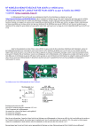
New
bhi DSP Noise Cancellation Products
for Radio and Voice Communications
www.bhi-ltd.com
NEDSP900
Preliminary Datasheet/User Manual
Main Features:
• Dual channel configurable Noise Suppression
• 30 dB AGC in channel 1 switchable
• Up to 30 dB maximum gain configurable input amplifiers
• Low power consumption (typ <5mA)
• Wide supply voltage range (3 to 20V)
• In‐and outputs RF protected with LC low pass filter
• Up to 40dB noise suppression
• Audio bandwidth 300Hz to 5KHz
Applications:
• Noise Cancelling Microphones
• Noise Suppression for radio voice communications
• Noise Cancelling in voice recognition to improve accuracy rates
• Intercoms
Issue:3
21‐11‐2013
NEDSP900
User Manual
1. Introduction
The NEDSP900 is a dual channel audio Noise Suppression pcb module capable of handling a wide
range of audio inputs and providing up to 40dB of noise suppression.
The module operates on a single supply rain with on‐board voltage regulation and clock oscillator. It
has low power consumption which makes it suitable for portable applications.
The noise suppression is carried out using a Digital Signal Processing (DSP) device that runs software
containing a CNS Noise Suppression algorithm. This is patented technology for noise reduction of
speech signals. It is known as one of the best algorithms of its kind and is ideally suited for real‐time
processing in any kind of voice communication system in noisy environments, such as handsfree
telephone sets, industrial intercom systems and radio communication systems.
2. Module Outline
The module comprises a multi‐layer PCB that provides good signal isolation and grounding making
integration into target systems easy with the minimum of design effort. A few simple rules need to
be observed in order to preserve the achievable levels of noise suppression, these are dealt with
later in this document. Pins are on a 2mm pitch.
Fig 1: View looking down on top of module showing basic dimensions and pin designations
2
Issue: 3
NEDSP900
User Manual
3. Pin Designations (see fig1)
From the annotated module outline fig1 on the previous page, the pattern of the pin‐outs provides
the user with good signal separation that can be continued easily on any board designed to carry the
analogue and digital interface electronics.
Pin
1
2
3
4
5
6
7
8
9
10
11
12
13
14
15
16
17
18
19
20
21
22
23
24
25
26
Designation
+ve Supply
GND
Cnl 1 NS On/Off
Cnl 1 NSL Bit 2
Cnl 1 Gain Bit 0
GND
Audio 1 Out
Audio 2 Out
GND
GND
Audio 1 In
GND
Audio 2 In
GND
Cnl 1 Gain Bit 1
Cnl 1 Gain Bit 2
Cnl 2 Gain Bit 0
Cnl 2 Gain Bit 1
S.F.
Cnl 1 NSL Bit 0
Cnl 1 NSL Bit 1
Cnl 2 NSL Bit 0
Cnl 2 NSL Bit 1
Cnl 2 NSL Bit 2
Cnl 2 NS On/Off
Cnl 1 AGC On/Off
Function
Positive supply input
Ground ‐ Power
Channel 1 Noise Suppression On/Off
Channel 1 Noise Suppression Level control Bit 2
Channel 1 Input Gain control Bit 0
Ground –use for Analogue/Digital Isolation
Channel 1 Audio Output
Channel 2 Audio Output
Ground – for use with Audio I/O Isolation
Ground – for use with Audio I/O Isolation
Channel 1 Audio Input
Ground – for use with Audio Inputs
Channel 2 Audio Input
Ground associated with Control Signals
Channel 1 Input Gain control Bit 1
Channel 1 Input Gain control Bit 2
Channel 2 Input Gain control Bit 0
Channel 2 Input Gain control Bit 1
Special Function – Algorithm ‘Hold/Run’
Channel 1 Noise Suppression Level control Bit 0
Channel 1 Noise Suppression Level control Bit 1
Channel 2 Noise Suppression Level control Bit 0
Channel 2 Noise Suppression Level control Bit 1
Channel 2 Noise Suppression Level control Bit 2
Channel 2 Noise Suppression On/Off
Channel 1 Automatic Gain Control On/Off
Use
+5V to +20V supply
Associated with Supply
Internal Pull Up
Internal Pull Up
Internal Pull Up
DC Isolated
DC Isolated
DC Isolated
DC Isolated
Internal Pull Up
Internal Pull Up
Internal Pull Up
Internal Pull Up
Leave open*
Internal Pull Up
Internal Pull Up
Internal Pull Up
Internal Pull Up
Internal Pull Up
Internal Pull Up
Internal Pull Up
*‐ S.F . Pin 19. – Leave this pin un‐connected. See para 14.
4. Power Supply
Pin 1 (+Ve Supply) is the device power pin. The module has an ‘on‐board’ regulator providing the
internal circuits with a regulated supply. The regulator requires a minimum of +3V to provide good
regulation and can handle up to +20 Volts Maximum. Due to size constraints the module is not
fitted with reverse voltage protection or current limiting circuitry, therefore it is recommended that
connections are checked well before applying power to the module.
3
Issue: 3
NEDSP900
User Manual
The module takes approximately 7mA when fully operational.
It is recommended that, if the module is to be used with other interface circuitry be it buffering the
analogue or digital signals, that further local supply suppression is used between Pins 1 and the
nearest ground (Pin 2 is ground). This should be carried out in line with common engineering
practices. A set of values of 10uF (Tantalum or Low ESR electrolytic), 100nF Ceramic and 10nF
Ceramic should be considered.
If it is expected that the Power Supply are to be very noisy, then consider fitting a ‘Pi’ filter network
close to Pins 1 and 2. Again this is a common practice.
5. Audio
All audio Inputs and Outputs have Radio Frequency (RF) filters to minimise the risk of EMC problems
when used in high – RF Environments such as communication systems.
Dependant on the modules use, the audio signals may be at very different levels, this is very likely to
be the case between the Audio Inputs and Outputs, but also may be the case between the two audio
channel inputs (if for instance a microphone is being used on Channel 1 and a Line level is being used
on channel 2). Minimise the possible cross‐talk between all the channels in line with common audio
practices.
6. Digital
The digital control pins are all pulled up internally (via several hundreds of kilo‐Ohms). In operation
the pins are normally pulled down to ground. Pins or functions that are not used can be left with the
appropriate pin ‘floating’. However, in applications where external interfacing is being used or the
electrical environment is noisy, the pins may be pulled up, using a much lower resistance (say a few
10’s of kilo‐Ohms) to a supply of no more than 1.8 Volts referenced to ground.
Functionality
The following sections deals with the basic device functionality and what settings can be made.
7. Audio Gain
The two audio channels are independent and have individual input gain setting facilities.
Channel 1 is recommended for Microphone signals as this has up to 30dB of selectable gain and a
unique AGC control. Channel 2 has its gain limited to +18dB. This makes the module useful for
many applications that involve processing either Stereo Audio signals or two different Audio signals
such as Microphone signal and a Receiver audio signal (as would be found in a communication or
Intercom system).
4
Issue: 3
NEDSP900
User Manual
Note:
Two important things to note about the audio channels, firstly the Gain setting only takes place
when the module initialises. This means that any change in audio Gain setting can only be done
before powering the module. Secondly, due to the design of the DSP device silicon, at 0dB audio
gain selection, there may be up to 9dB of insertion loss between the module input and output.
8. Channel 1 Gain
Gain (dB)
0
12
15
18
21
24
27
30
Module Pin 16/
Gain Bit 2
1
1
1
1
0
0
0
0
Module Pin 15
Gain Bit 1
1
1
0
0
1
1
0
0
Module Pin 5
Gain Bit 0
1
0
1
0
1
0
1
0
Note: ‘1’ is pin left open or pulled up to 1.8V, ‘0’ is pin pulled to ground.
9. Automatic Gain Control (AGC)
Like the other control pins, pin 26 (Cnl 1 AGC On/Off) requires pulling to ground to invoke the AGC
action on. Leaving this pin unconnected or high will inhibit the AGC action.
Note: The AGC control pin does not require the module to be re‐powered to take effect.
The AGC action makes use of the full 30dB Gain range and as such inhibits any pre‐set gain. When
operating it keeps the audio output level within 10dB of the maximum module output level, no
matter how much the input level is varying.
The AGC has a unique action, in that it recognises speech in a similar way to that of the Noise
cancellation programme. If there is no speech present, the AGC tends to hold the audio gain until it
next recognises a speech pattern. This holding of the Gain setting means that the audio does not
suddenly increase or start to ‘breath’ when the speech disappears. Any small amount of
recognisable speech will start the AGC tracking again.
10. Channel 2 Gain
This channel has less gain and therefore unsuitable for direct connection to a microphone, however,
it does still have sufficient gain to be used with many low level output devices such as receiver
detectors.
5
Issue: 3
NEDSP900
User Manual
The gain settings for Channel 2 are as follows:
Module Pin 18 Module Pin 17
Gain (dB)
Bit 1
Bit 0
0
1
1
12
1
0
15
0
1
18
0
0
Note: ‘1’ is pin left open or pulled up to 1.8V, ‘0’ is pin pulled to ground.
11. Channel Overloading
The module handles large input signals quite well. However, the user should try and keep their
maximum input levels below 1 Volt peak to peak (with gains set to 0dB). Above this value, a set of
protection diodes will act and the audio will sound distorted, however it will still continue to
operate.
Unfortunately, there are no overload indications available from the module and it is left up to the
user to ensure that the maximum module limits are adhered to or an overload detector is provided
to warn of such situations.
12. Noise Suppression
The noise suppression of each channel may be selected independently.
There are 8 levels of noise suppression per channel plus each channel may have its noise
suppression switched off.
Channel 1
Channel 2
Attenuation
(of white noise ‐ dB)
8
12
16
20
25
30
35
40
Module Pin 4
Module Pin 24
Bit 2
Module Pin 21
Module Pin 23
Bit 1
Module Pin 20
Module Pin 22
Bit 0
1
1
1
1
0
0
0
0
1
1
0
0
1
1
0
0
1
0
1
0
1
0
1
0
13. Noise suppression ON/OFF
The noise suppression function may be switched off on either channel. This is accomplished using
Pin’s 3 for channel 1 and Pin 25 for channel 2. Like the other control pins, to invoke noise
6
Issue: 3
NEDSP900
User Manual
suppression on the channel take the appropriate pin down to ground. Allowing the pin to float will
inhibit the noise suppression.
14. S.F. ‐ Pin 19 (Special Function)
The Noise Cancellation programme has a special function built in to allow it to be used in PTT
intercom systems. This special function pin enables the noise cancellation to held at the current
value. When the pin is released (allowed to float to 1.8 Volts), the algorithm continues where it left
off. This is very useful when the module is used in a half duplex intercom system. More information
available on request.
15. Electrical Characteristics
Absolute Maximum Ratings:
Power Supply Voltage: +24V; Negative voltage is not allowed
Maximum voltage at Digital Inputs: > ‐0.2; <1.8V
Maximum Voltage at Analogue outputs >0v; <2V
Maximum Ambient temperature: ‐50˚C to +100˚C
Storage Temperature: ‐55˚C to +150˚C
Operating Ratings: ‐40˚C to +85˚C
Parameter:
Supply Voltage
Power consumption
Audio Channels
Sampling Rate
Audio Bandwidth
Input:
Input Level (Max.)
Input Resistance
Output:
Output Level
Output Impedance
Signal to Noise Ratio
Total Harmonic
Distortion (THD)
Crosstalk between
output channels
Power supply rejection
Ratio
Input to output latency
Symbol
Vs
I
Value
3 to 20 Volts
Approx. 7 mA
2
16KHz
300Hz to 5KHz
Vin
Rin
700mV (eff)
550kΩ
Vout
Rout
SNR
220mV (eff)
12kΩ
>60dB
k
0.4%
20Hz to 20kHz; Measured at max.
Amplitude
Measured at 70% of max. amplitude
>55dB
Measured at maximum amplitude
>70dB
At Vs=5V; 1V ripple 20Hz to 20KHz
During operation of noise cancellation
At 0dB input gain setting
25mS
7
Issue: 3
Remarks
NEDSP900
User Manual
16. Background information on the DSP Noise Cancelling
Automatic Gain control
Automatic Gain control (AGC) selects the optimal input gain according to the input level. For low
input signals the AGC Increases the gain up to 30dB, whereas the AGC only cares for the voice
content. The noise floor during speech pauses is disregarded due to the algorithm only looking for
speech patterns.
CNS Noise Suppression
The CNS Noise suppression is capable of distinguishing between voice and noise components of an
audio signal. One of the signal properties being monitored is the modulation frequency of each
spectral component of the input signal.
Analysis of human speech yields typical modulation frequencies in the range of 2Hz to 5Hz. The idea
of the noise cancellation algorithm is that the signal components that switch modulation frequencies
in said interval, pass the system nearly without attenuation, while signal components with higher or
lower modulation frequencies as classified as noise. Such components are attenuated independency
of a selectable parameter. Figure 1 shows the modulation characteristic of the system measured
with amplitude modulated white noise, shown for 3 different values of the Noise Suppression
parameter.
8
Issue: 3
NEDSP900
User Manual
17. Applications
The following section deals with the basic common practice requirements for integrating the
NEDSP900 module into a system.
A.
Layout considerations
The NEDSP900 board is designed to provide a plug‐in solution for noise cancellation. The board itself
is designed to provide the best immunity from electrical noise and the best inter channel isolation,
while giving the user plenty of latitude in way to incorporate the board into their system.
It’s recommended that a good quality double sided PCB is used for the layout with good grounding
throughout any circuitry preceding or following the module. Any ground areas should be solidly
connected with all others to ensure good grounding system.
As previously stated, while the power pin is decoupled within the module, it is recommended that
further decoupling is employed between pins 1 and 2 of the module. A set of parallel capacitors
with values 10uF, 100nF and 10nF should be employed. If the supply rail is to be used for other
circuits, further decoupling capacitors of appropriate values should be employed locally at these
circuits as well.
In particularly noisy supply systems, use of individual ‘Pi’ filtering on the power supply lines should
also be considered to de‐couple the more sensitive devices.
B. Audio Lines
When placing audio tracks to and from the module pins, try to make as much use of the way in
which the ground pins are provided to ensure isolation between the audio signals and the digital
control signals.
Connecting Microphones
Only channel 1 (Pin 11 Signal /Pin 10 or 12 Ground) supports very low level inputs such as those
provided by microphones. Almost any type of microphone may be used including low impedance
(Circa. 300R or less) magnetic devices or higher impedance (1k0 or more) Electret inserts.
In the case of magnetic microphones, many of these have very low output levels of between 2mV
and 5mV. With these signal levels you will probably need the highest gain available on audio
channel 1. This will require all the ‘Chl1 gain’ pins to be grounded to provide the 30dB of gain.
In the case of Electret microphones, these can produce up to 20mV and therefore lower gains may
be selected such as 21dB through to 27dB. Note that the module does not provide a bias voltage for
electret microphones and this will have to be provided as part of the circuit into which the module is
to be integrated. The manufacturer of the Electret module will usually provide the appropriate bias
requirements and how to meet them. The NEDSP900 audio input is DC isolated already, alleviating
the need for extra DC Isolation capacitors being required between the microphone output and the
module.
9
Issue: 3
NEDSP900
User Manual
When using microphones for close in operation i.e. headset systems or desk microphones, it may be
worth trying the modules AGC option – see section 9.0 of this manual.
Higher level input signals
Because the NEDSP900 has a wide range of gain settings, it is configurable for many types of input
signal levels, however, if the module is to be used with speaker or headset output levels for instance
an MP3 player or a mobile radio set, consideration should be given to the use of a potential divider
network. The use of such a network will allow the system supplying the signal to be correctly loaded
and for the signal to be reduced to adequate levels required for the NEDSP900 input. Note that at
0dB gain setting on either audio channel the maximum input signal level is approximately 900mV p‐
p.
Audio Output
The NEDSP900 has an output impedance of around 12KOhms, therefore if the maximum output
level (approx. 500mV p‐p) is too much for the following circuitry, then a 10 KOhm or 20 KOhm
trimmer or volume control may be used to adjust the signal to attain the correct level. Do not use
any resistance values of less than 10K Ohm as this may cause damage to the output circuitry.
Using with Balanced Audio
The module has an unbalanced signal input and output. This may be a problem for some that have
balanced audio inputs or
feeds that need to be
balanced.
Input
If the input signal
level and impedance
allows, the simplest
option is to use a
balanced audio transformer. Apart from producing the balanced to unbalanced input
transformation, the transformer also provides good RF immunity.
For very low level input signals, such as balanced magnetic microphones, it may be
necessary to use an active balanced to unbalanced transformation. This can be
accomplished using simple Op‐amp circuits such as the one given here.
If higher gain and immunity from induced electrical noise is required then a 3 Op‐amp
Instrumentation Amplifier may be required. In all cases, RF immunity components should be
added.
10
Issue: 3
NEDSP900
User Manual
Output
The module output impedance is nominally 12 KOhm. This means that driving a low
impedance balanced line will require buffering before using an unbalanced to balanced
transformer.
Alternatively,
depending on the
grounds within the
system, it may be
possible to use an
unbalanced to
balanced Op‐Amp
circuit.
If using the later
solution ensure that
extra RF immunity
components are added.
C. Control Lines
The control lines are pulled up internally via several hundreds of kilo‐Ohms. If using the module with
an active control system (i.e. not using It is important that these lines are not driven beyond 1.8
Volts or below ‐0.3v negative as the main device will be damaged.
All control GPIO lines should be dressed away from the module and away from any audio input or
output lines in order to minimise the likelihood of digital interference to the audio signals.
18. Controlling the device
There are two ways in which the device can be controlled. The module has been designed
such that it may be used with purely passive control elements such as switches or solder
pads. To get to know the module functionality its worthwhile hooking it up with a set of DIP
switches. Using these allow the quick re‐configuration of the module functions with the
minimum of fuss.
11
Issue: 3
NEDSP900
User Manual
Typical NEDSP900 test circuit
Note: the use of switches allows quick re‐configuration of the NEDSP900 for testing. When the switches close the
function is selected.
The use of jumper pins or PCB solder patches are recommended for applications where the
board is to be integrated into a larger system or where the configuration is likely to be fixed,
but may need modifying.
Logic control
There are several ways in which the module may be controlled by external logic or
microprocessor. The simplest is to use a transistor to pull the appropriate pin to ground.
The collector load and supply is provided by the module itself and all that is required is the
appropriate drive to the transistor base. Alternatively, there are logic transistors that will
perform this function without the need for any additional resistors.
Many processors may also drive the module directly as they already have full pull up/pull
down outputs that use MOSFET’s. There are two approaches to this. This simplest is to use a
diode placed with it’s anode to the module pin and cathode to the processor pin. When the
processor pin goes high the diode is back biased and the module pin is allowed to float.
When the processor pin goes low the diode conducts and the module pin is pulled low. This
is simple and usable where the processor supply is up to 5 Volts. If the processor is powered
using 1.8 Volts or lower, the likelihood of the diode being back biased is small and therefore
Logic transistors may be the path to take.
12
Issue: 3
NEDSP900
User Manual
The alternative method to using a diode is to use a potential divider network. This will
ensure that the module pin is pulled low without a processor being connected. When the
processor pulls high, the resistor network needs to be able to divide the processor output
down to a maximum of 1.8 Volts.
From logic or
To module
processor output
R2
pin
R1
Processor supply
3.3v
5v
R1 Ohms
1K
1K
R2 Ohms
820R
1.8K
13
Issue: 3
NEDSP900
User Manual
Contact details:
bhi Ltd
22 Woolven Close
Burgess Hill
West Sussex
RH15 9RR
Tel: +44 (0)1444 870333
Fax: +44 (0)845 2179936
Email: sales@bhi‐ltd.com
Web: www.bhi‐ltd.com
14
Issue: 3