1
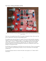
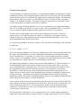
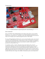
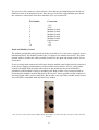
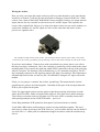
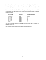
Oakley Sound Systems
Oakley Modular Eurorack Series
RM-4014 Ring Modulator
PCB Issue 3E
Builder's Guide
V3.1.0
Tony Allgood
Oakley Sound Systems
CARLISLE
United Kingdom
Introduction
This is the Project Builder's Guide for the issue 3E RM-4014 Ring Modulator Euro module
from Oakley Sound. This document contains a basic introduction to the board, a full parts list
for the components needed to populate the board, a circuit description, and a list of the
various interconnections.
For the User Manual, which contains an overview of the operation of the unit and the
calibration procedure, please visit the main project web page at:
http://www.oakleysound.com/ringmod-e.htm
For general information regarding where to get parts and suggested part numbers please see
our useful Parts Guide at the project webpage or http://www.oakleysound.com/parts.pdf.
For general information on how to build our modules, including circuit board population,
mounting front panel components and making up board interconnects please see our generic
Construction Guide at the project web page or http://www.oakleysound.com/construct.pdf.
2
The Issue 3E Ring Modulator PCB
This is the issue 3E Euro sized Ring Modulator board fully populated and awaiting panel mounting and
sockets wiring.
This is one of our smaller format PCBs. The module is designed to fit into a Euro rack. The
pots are Alpha/ALPS 16mm types with matching brackets.
The module requires plus and minus 12V supplies. The power supply should be adequately
regulated. The current consumption is about +/-38 mA. Power is routed onto the main PCB
via the usual 2 x 5 way 0.1” (2.54mm) header for compatibility with Euro format modular
systems. The top pins on the header are connected to the +12V supply. Reverse polarity
protection diodes have been fitted although these should not be relied upon to protect your
module for a long period of time.
The PCB has four mounting holes for M3 bolts, one near each corner. These are not required
if you are using our specially made pot brackets. The size of the board is 96.5mm high by
86.4mm deep.
The input and output sockets are wired to the board via an eight way 0.1” Molex or MTA
interconnect.
3
Ring Modulator issue 3E Parts List
For general information regarding where to get parts and suggested part numbers please see
our useful Parts Guide at the project web page or http://www.oakleysound.com/parts.pdf.
The components are grouped into values, the order of the component names is of no particular
consequence.
A quick note on European part descriptions. R is shorthand for ohm. K is shorthand for kiloohm. R is shorthand for ohm. So 22R is 22 ohm, 1K5 is 1,500 ohms or 1.5 kilohms. For
capacitors: 1uF = one microfarad = 1000nF = one thousand nanofarad.
To prevent loss of the small ‘.’ as the decimal point, a convention of inserting the unit in its
place is used. eg. 4R7 is a 4.7 ohm, 4K7 is a 4700 ohm resistor, 6n8 is a 6.8 nF capacitor.
Resistors
All 5% carbon 1/4W or better, except where stated.
220R
470R
680R
1K
4K7
10K
12K
15K
18K
39K
56K
1M
2M2
R20
R19
R6, R16
R10
R22, R4
R9, R1, R2, R8
R14
R11
R7, R15, R18
R3, R21
R13
R12
R5, R17
Capacitors
15pF 2.5mm C0G ceramic
47pF 2.5mm C0G ceramic
100nF axial multilayer ceramic
1.5uF or 2u2, 63V or 50V polyester
2.2uF, 25V electrolytic
C11
C3
C7, C8, C9, C10, C15, C16
C1, C6
C4, C17, C13, C14
4
Discrete Semiconductors
1N4004 rectifier diode
1N4148 signal diode
BC550 NPN transistor
BC560 PNP transistor
D7, D8
D1, D2, D3, D4, D5, D6
Q2, Q4
Q1, Q3
Integrated Circuits
TL072 dual op-amp
THAT320P PNP array
THAT300P NPN array
U2, U3
U1
U4
Variable Resistors
50K or 100K multiturn trimmer
BAL1, BAL2, GAIN
100K linear Alpha 16mm pot
50K linear Alpha 16mm pot
X-LEVEL, Y-LEVEL
Y-OFFSET
Pot brackets
Three off
Miscellaneous
Leaded ferrite beads
L1, L2
2 x 5 (10-way) 0.1” box header
PSU
0.1” 8-way Molex or MTA header SOCKETS
0.1” 8-way Molex or MTA housing SOCKETS
DIL14 pin IC sockets
DIL 8 pin IC sockets
– board mounted
– wire harness
Two off
Two off
Other Parts Required
3.5mm sockets
Five off mounted on panel
Three 20mm knobs.
Around 2m of insulated multistrand hook up wire for the socket connections.
5
Circuit description
A ring modulator is sometimes described as a four quadrant multiplier, and while this certainly
sounds more grand, it also explains the action of the device in more detail. The four quadrants
refer to the four quarters of a standard XY graph with the origin in the middle. The idea being
that this device allows two inputs, we will call them X and Y, of either positive or negative
voltage, to be multiplied together. The output is therefore either positive when both X and Y
are the same polarity, or negative when they are different.
A standard voltage controlled amplifier (VCA) can be considered as two quadrant multiplier
since one of its inputs can only be of a positive value. The two quadrants where Y is negative
are not computed, and the output normally remains at zero when Y is not positive.
In audio when an input signal is processed so that it changes from a positive value to a
negative one we say it has been inverted, or that it is 180 degrees out of phase with the
original. In this way, a ring modulator may be considered to change the phase of one of its
inputs depending on the polarity of the other.
In a perfect ring modulator the inputs X and Y can be considered as having the same functions
as each other.
ie. X x Y = output = Y x X
In our real life ring modulator this is not true. Imperfections in the circuit topology means that
the output will sound different, or behave differently, depending on which signal you insert
into X and which into Y. Generally, we will use X as our input signal (sometimes called the
carrier), and Y as our modulator. That is, Y will shape X. In many applications it doesn't make
too much difference which is which, so experimentation is the key here.
The Oakley Ring modulator is based around the old ARP module 4014. This was built on an
incredibly tightly cramped circuit board which was then securely potted, with a very hard
epoxy compound, into a small plastic box. The various interconnections were made to some
thin gold plated legs that stuck out from the hard epoxy on the underside. It is almost
impossible to remove the circuitry from its hard plastic shell and all encompassing resin. I
suppose this was mostly down to Alan Pearlman's previous history in making op-amps for the
aerospace industry – enclosing circuits like this would make them less likely to drift with
temperature and be affected by surrounding humidity. However, one might also think that they
did it to keep out the prying eyes of their competitors.
Later versions of the 4014 used soft and rubbery silicone to pot the circuitry into its shell with
only a thin layer of epoxy on the underside to seal it all in. These are easier to repair since it is
now possible, with great care, to remove the delicate circuitry from its shell and potting
compound. Various folk have since reverse engineered this circuit and it can be found in
various places on the internet.
The basic function of the 4014 is of two complementary VCA circuits, both controlled by a
single driver, and each feeding a common current to voltage output stage. The driver features
6
a non linear gain that acts as a pre-distortion device which compensates for some of the non
linearities in the VCA sections.
The very first Oakley ring modulator module built to replace a dead ARP-4014 module in an ARP2600
synthesiser. The Oakley RM-4014 module borrows heavily from the design shown here.
U3, a dual op-amp, is configured as two voltage followers, one for each input. The signal level
to each one is controlled via its own level pot. The source of the signal can come from either a
direct coupled input via a single resistor, or AC coupled via a capacitor. The capacitor in
conjunction with the resistor following it and the pot itself will act as a high pass filter. This
will attenuate very low frequency signals with a -3dB point of around 1Hz. It is possible to use
both the AC and DC inputs simultaneously thus creating a crude two channel mixer. However,
although no harm to the unit will come about, it does cut down the overall signal level
presented to the input level pot.
Both U3 halves act as protective buffers for the relatively high output impedance of the level
pots. The lowish input resistances of the ring modulator input stages would otherwise
detrimentally affect the pots' apparent taper, the cut-off frequency of the AC coupled input,
and perhaps also the output stage of the connected modules.
The ring modulator core is built from two transconductance amplifiers that are complementary
to one another. A transconductance amplifier is basically a 'voltage in, current out' device
whose gain, in this case, is controlled by another modulating current. And complementary in
this definition means identically opposite, mirrored if you like. In other words they behave
7
mostly the same but one is modulated by positive currents from the driver, the other negative
currents. Since the driver is common to both of them and its own output is either positive or
negative, only one of the transconductance stages is active at any one time.
I have tried to draw the schematic so you can see the two complementary halves of the core
easily. Each one appears identical but for the type of transistors used. Where one uses a NPN,
the other will use a PNP, and vice versa. Note too, that the X input is applied to different sides
of the transconductance stages resulting in one of them being of opposite phase to the other.
The left hand side deals with Y modulation signals that are positive in value. The right hand
side deals with Y modulations that are negative in value.
Each transconductance amplifier is made from five transistors. Four are two sets of matched
pairs. A matched pair is exactly that; two devices that share with almost identical
characteristics. This cannot usually be obtained from simply buying two transistors of the same
type, since in manufacturing there are small discrepancies that make every device slightly
unique. In the original 4014 module, ARP would have hand selected their transistors by trying
hundreds out and grouping them together into large bins with contained those devices with
similar characteristics. Each pair would then be made by selecting two devices from the same
bin. This would take too much time when you only want to build one or two Oakley Ring
Modulators, so I have used pre-matched quad transistor arrays. The THAT300 is four
matched NPN transistors, and the THAT320 is four matched PNP transistors. The electronic
matching is near perfect and they are also made onto the same silicon die and in the same
housing thus ensuring a good thermal matching too.
The voltage at the top of each transconductance stage is fixed by diodes to be 1.2V for the left
hand side one and -1.2V for the right hand side. C4 and C17 provide some additional
decoupling to reduce any noise or audio signal bleedthrough at these points. C4 and C17 were
not in the original design, but I have added them here to reduce any chance of extraneous
noise pick up.
The output of both transconductance stages go to the inverting input of the output op-amp,
U2, pins 1, 2 and 3. This is wired as an inverting transimpedance amplifier, which is a 'current
in, voltage out' device and essentially the opposite of a transconductance amplifier. A
transconductance amplifier followed by a transimpedance amplifier make an amplifier, ie.
'voltage in, voltage out'.
To make sure the overall gain of the ring modulator is positive for Y being positive, we use
the inverting outputs from each transconductance amplifier. These are found on the collector
of the left hand transistor of the input pair, ie. U14, pin 14 and U1, pin 7.
The gain of the transconductance amplifiers is controlled by the driver circuit. The output of
the driver circuit is converted to a current by R18 which in turn affects the current through the
input pairs and hence the amplitude of the current output. However, the response of gain
versus input current is not linear when the output of U2 is less than 0.6V for the left hand
amplifier and above 0.6V for the right hand one. This is because to control the gain of the
transconductance amplifiers the voltage at the bottom of R18 must be enough to overcome the
inherent base-emitter voltage and turn on either of the input transistor pairs. This would give
rise to a dead zone of operation if it were not for the deliberate non linearity introduced in the
driver circuit.
8
Q3 and Q4 are wired as diodes in the feedback of the driver op-amp. This means for output
voltages between -0.6V and +0.6V the gain of the op-amp is very high indeed as it is pretty
much set solely by the ratio of R12 and R11. Thus even a small voltage on the Y input will
lead to either +0.6V or -0.6V depending on the polarity of the input. Once this voltage has
been achieved any increase in input voltage will decrease the gain as either Q3 or Q4 turns
increasingly on. Eventually, the gain tends to the ratio of R15 and R11, a much smaller figure.
Unlike the original circuit application, the Oakley Ring Modulator allows you to add a positive
offset voltage to the Y input voltage. Thus effectively increases the gain of the left hand
transconductance amplifier thus allowing the non inverted X signal to pass through to the
output even when no positive Y input is present.
Power is supplied via the usual 10-way 0.1” header. As is the custom for Oakley modules, I
have used ferrite beads to act as high frequency filters on the power lines. Decoupling at the
point of entry is provided by C13 and C15 for the positive rail, and C14 and C16 for the
negative rail. Additional decoupling is also provided elsewhere on the board by the other
capacitors shown at the bottom of the schematic. All these capacitors keep the power supply
clean of noise, and provide a reservoir for the little bursts of current that the circuit takes in
normal operation.
D7 and D8 provide some protection against the power lead being connected in reverse.
9
Connections
Power is admitted to the module via a boxed 10-way IDC header. The sockets are connected via an
optional 8-way Molex 'strip and crimp' style 0.1” header and housing.
Power connections
Power is provided via the standard Doepfer power header system. This is a 10 way header
based on a 2 x 5 0.1” grid. It is not typical to use a boxed keyed header as Doepfer uses an
unenclosed set of pins. However, I, and others, prefer these shrouded headers as it lessens the
chance of reversing the power lead and frying the electronics of the module.
The issue 3E Ring Modulator PCB does have reverse protection diodes. In the event of power
reversal these will conduct and draw a large amount of current. This should cause the power
supply to go into current limit. However, this current may be large enough to eventually burn
out the diodes and damage them. The protection diodes are therefore only suitable for
protection for a short period of time.
It is possible to replace L1 and L2 with quick acting semi-conductor fuses. I am not
experienced in using these devices but other designers have used them with success. When
activated they will effectively reduce the current taken by the diodes and protect all the
components on the module for a great deal longer than the diodes would on their own. I'll be
glad to hear of people's experiences with these devices if you do choose to use them. Bear in
mind though that when the fuses are not tripped they do still have some resistance. This small
resistance will reduce the voltage to the module a bit and this may have some audible affect.
10
The pin out for the connector is shown below. Note that the pin numbering of the header are
different to that of an integrated circuit. Here they go from left to right and then move down
the connector, rather than count down and then up as you would an IC.
Pin Number
Connection
1
2
3
4
5
6
7
8
9
10
+12V
+12V
Module Ground
Module Ground
Module Ground
Module Ground
Module Ground
Panel Ground
-12V
-12V
Panel and Module Ground
The module ground and panel ground are both connected to 0V at the power supply or power
distribution board. The module ground is the 0V supply to the module electronics. The panel
ground, while it is still at the same potential, connects to the input and output sockets' screen
connection.
If you are using metal sockets this will ensure that the module panel is then directly connected
to the power supply's ground and not via the module's more sensitive 0V line. Using plastic
sockets will simply float the panel with respect to the module but the panel will then be
grounded via the modular's casing or mounting rails. Both of these ways seem preferable to
connecting the module's sockets and panel to the local 0V where ground currents could travel
down any patch cable's screen connection. But in either case any Oakley module wired in such
way will still be compatible with any other Euro module.
The current version of the Krisp1 Oakley Ring Mod. Older versions have only two input sockets and two
switches.
11
Wiring the sockets
How you wire your input and output sockets up will very much depend on your panel design
and choice of sockets. I will only go into the details of wiring up a panel with the five 3.5mm
sockets. One variant of the Krisp1 built RM-4014 uses only three sockets, one output and two
inputs, but has also two switches to select between AC and DC inputs. This replicates the
circuit of the original 2600. However, by using four input sockets you can use the module as a
crude mixer. Both the AC and DC inputs are active at the same time and can be used to
process two signals at once.
The standard 3.5mm chassis mount socket. The metal bush means that the panel will be electrically
connected to the socket's ground lug. The ground lug is the one that sticks out from the side of the socket.
If you have used ordinary 3.5mm sockets with a metal bush (see picture above) you will see
that they have three connections. One is the earth lug or ground tag, which connects the metal
mounting bush. The second is the signal tag which will be connected to the tip of the jack plug
when it is inserted. The third tag is the normalised tag, or NC (normally closed) lug. The NC
lug is internally connected to the signal tag when a jack plug is not inserted. This connection is
automatically broken when you insert a jack. We shall not be using the NC lugs at all on this
module.
Firstly, we are going to ‘common’ the sockets’ ground lugs. This means that the sockets’
ground lugs are going to be joined together. I normally do this part of the wiring without the
PCB or pots in place on the panel.
Fit the five input signal sockets onto the panel so that the ground tag sticks down towards
where the PCB will be. Solder a length of thin solid core wire right across all the earth tags.
Trim off any excess that sticks out on either end. This wire will be eventually connected to
either panel ground pin on the SOCKETS header – pin 6 or 8.
Fit the Ring-modulator PCB against the front panel if you haven't done so already.
I used Molex KK headers and housings to connect my ring modulator together. This way I
don't have to solder my wiring to the PCB. However, you can solder directly onto the board if
you wish. The 0.1” solder pads are substantial enough to be able to solder the usual hook up
wire to.
12
Use multistrand hook up wire to connect each socket lug to the relevant pin on the header.
Keep your wires short but not too short and you can use as many different colour wires as you
can – although I tend to use one colour because I'm a minimalist. There is absolutely no need
to use screened cable for such short runs.
The connections of the lugs of the CV and audio output sockets that go directly to the PCB
are summarised in the table below. They are given in the order in which I would recommend
that they be soldered.
Socket Name
Lug type
Header Pin number
All sockets
IN X (DC)
IN X (AC)
IN Y (DC)
IN Y (AC)
XxY
Earth
Signal
Signal
Signal
Signal
Signal
6 or 8
1
2
4
5
7
Note: Pin 1 is the square solder pad on the PCB. All the other solder pads on the header are
round. Pin 3 is not used.
Once the wiring is done your module is ready for testing and calibration.
13
Testing, testing, 1, 2, 3...
Apply power to the unit making sure you are applying the power correctly. Check that no
device is running hot. Any sign of smoke or strange smells turn off the power immediately and
recheck the polarity of the power supply, and the direction of the ICs in their sockets.
Assuming everything is OK so far, it is time to apply an audio input. Use a signal like a
triangle output from a VCO. Middle A, 440Hz is a good note to use. Turn down all the pots
to their minimum setting and insert your triangle wave signal into IN X (AC). Listen to the
output signal from the ring modulator module. For the moment you should hear nothing.
Turn up the X LEVEL pot to full. Again, you shouldn't hear anything, but maybe you will
hear a little triangle wave bleedthrough. Now slowly turn up the Y OFFSET pot. If all is well
this should behave like a volume control, increasing the level of the triangle wave as it is
turned up.
Ensure that altering Y LEVEL should have no effect on the sound, but that X LEVEL
behaves also like a volume control. It should seem that both X LEVEL and Y OFFSET do the
same thing. They do not of course, since X LEVEL is altering the signal level going into the
ring modulator circuit, and Y OFFSET is adjusting the gain of the amplification within the ring
modulator.
Swap the input signal over to the IN X (DC) input. This should have no apparent effect on the
sound.
There is a very good chance your circuit is working correctly if you have got this far with no
problems. However, we still need to check a few other things and you'll need another signal
source to do this. Connect a LFO or VC-LFO to the IN Y (DC) input. Use a sine or triangle
wave signal at a lowish frequency, say 1Hz or so.
Turn the Y OFFSET down and the X LEVEL up. Now slowly turn the Y LEVEL up and
listen to the resultant sound. It should be the triangle wave you can hear again, but it will pulse
up and down with LFO signal. You should hear it go up and down in volume twice for every
cycle of the LFO, ie. at 2Hz if you have set your LFO to 1Hz. This is because, unlike an
ordinary VCA, the triangle wave is being multiplied by both the positive and negative parts of
the LFO's waveform. Thus you get a rise in volume with increasing positive voltages and a rise
volume with increasing negative ones.
If you increase the Y OFFSET pot to its maximum value, you should find that you now have
only one cycle of volume change per LFO cycle. The offset pot has added a positive voltage to
the Y input thus making it solely positive in value.
If all is well, then you have a working ring modulator module.
14
Final Comments
If you have any problems with the module, an excellent source of support is the Oakley Sound
Forum at Muffwiggler.com. Paul Darlow and I are on this group, as well as many other users
and builders of Oakley modules.
If you can't get your project to work, then Oakley Sound Systems are able to offer a 'get you
working' service. If you wish to take up this service please e-mail me, Tony Allgood, at my
contact e-mail address found on the website. I can service either fully populated PCBs or
whole modules. You will be charged for all postage costs, any parts used and my time at
25GBP per hour. Most faults can be found and fixed within one hour, and I normally return
modules within a week. The minimum charge is 25GBP plus return postage costs.
If you have a comment about this builder's guide, or have a found a mistake in it, then please
do let me know. But please do not contact me or Paul Darlow directly with questions about
sourcing components or general fault finding. Honestly, we would love to help but we do not
have the time to help everyone individually by e-mail.
Last but not least, can I say a big thank you to all of you who helped and inspired me. Thanks
especially to all the nice people on the SynthDIY and Analogue Heaven mailing lists and at
Muffwiggler.com.
Tony Allgood at Oakley Sound
Cumbria, UK
© May 2012 – updated September 2014
No part of this document may be copied by whatever means without my permission.
15