1
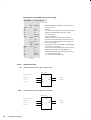
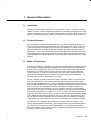
DEZ 161 Interrupt Processing, Discrete Input Module for A250 User Manual A91M.12-703500.20-0294 Translation of the German Description A91M.12-700224 Notes Application Note Caution The relevant regulations must be observed for control applications involving safety requirements. For reasons of safety and to ensure compliance with documented system data, repairs to components should be performed only by the manufacturer. Training AEG offers suitable training that provides further information concerning the system (see addresses). Data, Illustrations, Alterations Data and illustrations are not binding. We reserve the right to alter our products in line with our policy of continuous product development. If you have any suggestions for improvements or amendments or have found errors in this publication, please notify us by using the form on the last page of this publication. Addresses The addresses of our Regional Sales Offices, Training Centers, Service and Engineering Sales Offices in Europe are given at the end of this publication. Copyright All rights reserved. No part of this document may be reproduced or transmitted in any form or by any means, electronic or mechanical, including copying, processing or any information storage, without permission in writing by the AEG Aktiengesellschaft. You are not authorized to translate this document into any other language. Trademarks All terms used in this user manual to denote AEG products are trademarks of the AEG Aktiengesellschaft. 1994 AEG Aktiengesellschaft. ii 20 Terminology Note This symbol emphasizes very important facts. Caution This symbol refers to frequently appearing error sources. Warning This symbol points to sources of danger that may cause financial and health damages or may have other aggravating consequences. Expert This symbol is used when a more detailed information is given, which is intended exclusively for experts (special training required). Skipping this information does not interfere with understanding the publication and does not restrict standard application of the product. Path This symbol identifies the use of paths in software menus. DPM IR Dual-Port-Memory Interrupt Figures are given in the spelling corresponding to international practice and approved by SI (Système International d‘ Unités). I.e. a space between the thousands and the usage of a decimal point (e.g.: 12 345.67). Informational Objectives This manual describes the capability of interrupt processing and binary input of the digital input expert DEZ 161 as well as the linking of these activities to the A250 programmable controller. Our goal is that you should be able to realize interrupt processingwith the DEZ 161. Prerequisites are: Basic knowledge in configuration/design of the A250 programmable controller Basic knowledge in the programming of the A250 programmable controller in Dolog AKF → A120/A250 (AKF125) 20 iii Content Arrangement of this Publication Chapter 1 General Information This chapter describes structural elements of interrupt user programs and their effect on the runtime of the primary user program; it also contains instructions for the creation of IR user programs. The reader will learn about the cooperation betweenthe DEZ 161 hardware module incl. firmware and the DEZ-related standard function blocks (data structures). Chapter 2 Operation This chapter provides an overview of the indicator and operating elements on the DEZ 161 module. Chapter 3 Configuration/Design This chapter lists all required hardware and software that has to be in place to make the DEZ 161 operational all special conditions that must be observed when designing the programmable controller all steps necessary for configuration, parameterization and start-up of the module. Following the list of configuration steps is a detailed example of an IR application with actual task definition and hardware configuration as well as a description of the solution. At the end of this example is an FBD representation of the IN and OUT blocks. In presenting the software solution, an abbreviated method of writing was chosen to give the reader an opportunity for exact reconstruction of the parameter processing without the inconvenience of having to look at other pages. The detailed execution of above mentioned configuration steps is described in the respectiveuser manual of the A250 or U250 programmable controllers, or in the respective software package. iv Appendix A DEZ 161 Module Descriptions Appendix B O_INTR Block Description 20 Related Documentation Modicon A250 Compact Controller User Manual A91M.12-271 953 Dolog AKF → A120/A250 Typ AKF125 Version 2.0 Diskettes 3 1/2 ’’ and 5 1/4 ’’ User Instructions E-No. 424 275 181 A250 Dolog AKF Standard Function Blocks (AKF125 Version 2.x) Volume 1 (A to P) Block Library A91M.12-279384 A250 Dolog AKF Standard Function Blocks (AKF125 Version 2.x) Volume 2 (Q to Z) Block Library A91M.12-279385 User Manual U250, in preparation Operating instructions for software package PRO→ U250, in preparation 20 v Applicability The performance described in this manual represents performance level 1 of theDEZ 161 module (”digital input expert”), the EPROMs DEZ F01 and F02 are at revision status Rev. 0 Statements made for the SFBs refer to AKF125 Version 2.0 vi 20 Table of Contents Chapter 1 1.1 1.2 1.2.1 1.2.2 1.2.3 20 General Information . . . . . . . . . . . . . . . . . . . . . . . . . . . . . . . . . . . . . . . . . . . . 1 Performance Capability of the DEZ 161 . . . . . . . . . . . . . . . . . . . . . . . . . . . . . . . . . . . . . . . . . Path to Solutions with IR Processing . . . . . . . . . . . . . . . . . . . . . . . . . . . . . . . . . . . . . . . . . . . . Structural elements of IR user programs . . . . . . . . . . . . . . . . . . . . . . . . . . . . . . . . . . . . . . . . . Important SFBs and their impact on user program runtime . . . . . . . . . . . . . . . . . . . . . . . . . References to examples in IL and FBD format . . . . . . . . . . . . . . . . . . . . . . . . . . . . . . . . . . . 2 2 2 3 5 Chapter 2 Operation . . . . . . . . . . . . . . . . . . . . . . . . . . . . . . . . . . . . . . . . . . . . . . . . . . . . . . 7 2.1 2.2 Indicator Elements . . . . . . . . . . . . . . . . . . . . . . . . . . . . . . . . . . . . . . . . . . . . . . . . . . . . . . . . . . . . 8 Operating Elements . . . . . . . . . . . . . . . . . . . . . . . . . . . . . . . . . . . . . . . . . . . . . . . . . . . . . . . . . . . 8 Chapter 3 Configuration/Design . . . . . . . . . . . . . . . . . . . . . . . . . . . . . . . . . . . . . . . . . . . 9 3.1 3.2 3.3 3.3.1 3.3.1.1 3.3.1.2 3.3.1.3 3.3.2 3.3.2.1 3.3.2.2 3.3.2.3 3.3.2.4 3.3.3 3.3.3.1 3.3.3.2 3.3.3.3 3.3.4 3.3.5 3.3.5.1 3.3.5.2 3.3.6 Prerequisite Knowledge . . . . . . . . . . . . . . . . . . . . . . . . . . . . . . . . . . . . . . . . . . . . . . . . . . . . . . 10 Hardware and Software Requirements . . . . . . . . . . . . . . . . . . . . . . . . . . . . . . . . . . . . . . . . . 10 Steps for configuration/design . . . . . . . . . . . . . . . . . . . . . . . . . . . . . . . . . . . . . . . . . . . . . . . . . 11 Preparations to build the programmable controller (hardware) . . . . . . . . . . . . . . . . . . . . . 11 Requirements for the A250 . . . . . . . . . . . . . . . . . . . . . . . . . . . . . . . . . . . . . . . . . . . . . . . . . . . 11 Requirements for the U250 . . . . . . . . . . . . . . . . . . . . . . . . . . . . . . . . . . . . . . . . . . . . . . . . . . . 11 Procedure . . . . . . . . . . . . . . . . . . . . . . . . . . . . . . . . . . . . . . . . . . . . . . . . . . . . . . . . . . . . . . . . . . 11 Preparations for the programming of the programmable controller in AKF125 . . . . . . . 12 Requirements for the A250 . . . . . . . . . . . . . . . . . . . . . . . . . . . . . . . . . . . . . . . . . . . . . . . . . . . 12 Requirements for the U250 . . . . . . . . . . . . . . . . . . . . . . . . . . . . . . . . . . . . . . . . . . . . . . . . . . . 12 Procedure for the A250 . . . . . . . . . . . . . . . . . . . . . . . . . . . . . . . . . . . . . . . . . . . . . . . . . . . . . . . 12 Procedure for the U250 . . . . . . . . . . . . . . . . . . . . . . . . . . . . . . . . . . . . . . . . . . . . . . . . . . . . . . . 12 Example of IR Application with Block Linking . . . . . . . . . . . . . . . . . . . . . . . . . . . . . . . . . . . . 13 Configuration with task definition . . . . . . . . . . . . . . . . . . . . . . . . . . . . . . . . . . . . . . . . . . . . . . . 13 Solution presented in IL and/or FBD format . . . . . . . . . . . . . . . . . . . . . . . . . . . . . . . . . . . . . 15 Additional blocks . . . . . . . . . . . . . . . . . . . . . . . . . . . . . . . . . . . . . . . . . . . . . . . . . . . . . . . . . . . . . 18 Example of binary input . . . . . . . . . . . . . . . . . . . . . . . . . . . . . . . . . . . . . . . . . . . . . . . . . . . . . . 19 Preparations for the parameterization of the DEZ 161 (software) . . . . . . . . . . . . . . . . . . 19 Procedure for the A250 . . . . . . . . . . . . . . . . . . . . . . . . . . . . . . . . . . . . . . . . . . . . . . . . . . . . . . . 19 Requirements for the U250 . . . . . . . . . . . . . . . . . . . . . . . . . . . . . . . . . . . . . . . . . . . . . . . . . . . 20 Procedure for initial start-up . . . . . . . . . . . . . . . . . . . . . . . . . . . . . . . . . . . . . . . . . . . . . . . . . . . 20 Table of Contents vii Appendix A Module Descriptions . . . . . . . . . . . . . . . . . . . . . . . . . . . . . . . . . . . . . . . . . . 21 DEZ 161 Binary Input (Discretes In) . . . . . . . . . . . . . . . . . . . . . . . . . . . . 23 DCF 77E Receiver . . . . . . . . . . . . . . . . . . . . . . . . . . . . . . . . . . . . . . . . . . . . 33 Appendix B Block Description . . . . . . . . . . . . . . . . . . . . . . . . . . . . . . . . . . . . . . . . . . . . 39 O_INTR Interrupt-Processing 41 A250 Index . 47 viii Table of Contents 20 Chapter 1 General Information This chapter describes structural elements of interrupt user programs and their effect on the runtime of a primary user program.It also contains information on how to create IR user programs. The purpose of this chapter is to provide the reader with an understanding of the cooperation between the DEZ 161 hardware module incl. firmware and the DEZrelated standard function blocks (data structures) . 20 General Information 1 1.1 Performance Capability of the DEZ 161 Depending on firmware and parameter EPROMs and the cooperation with the required AKF user program of the ALU, the DEZ 161 is capable to process interrupts and binary input as well as count values and real-time events provided it is connected to a DCF receiver; refer to Appendix A, Ch. 1. This user manual is only treating the application relative to interrupts and binary<Sa><R> input with special consideration of interrupt processing;interrupts are simply described as ”binary input with a high priority”. All module-relative IR processing is carried out in a DEZ F01 firmware program, the parameterization of 16 interrupts and 16 discretes in (refer to Figure 2) is defined in a DEZ F02 parameter EPROM. Individual user programs can assemble and evaluate interrupt groups according to priority by utilizing the standard function block O_INTR of the basic ALU software. By suppressing unused IR discretes in with masks, optimum IR evaluation can already be achieved during initialization. The programmed DEZ F01 and DEZ F02 EPROMs are available and can be shipped when ordered. The outlined application sample case does not requirea DCF receiver. 1.2 Path to Solutions with IR Processing 1.2.1 Structural elements of IR user programs The standard function block O_INTR (SFB 392) that is part of the AKF125 provides users with a ”tool” which enables them to program their own interrupt evaluation programsfor the DEZ 161. The path runs via the OB1 organization block and with networks for one SFB call each of the O_INTR (for group assembly of interrupts, a max. of 4 networks, if assigning a max. of 4 interrupt groups) to additional networks and program blocks: During spontaneous occurrence of an expected interrupt (IR) within the assigned IR group, the SFB 392 triggers a user OBxxx which (in a network) identifies the respectively occurring IR and then activates the assigned program block PB xxx of the user through a conditional jump, refer to Figure 1. The user can utilize an interrupt for internal logic operations and to prepare future processing steps. However, in most cases an IR should very quickly trigger an action in the peripherals even before returning to the primary user program that was interrupted by the IR. Note The most immediate reaction in the peripherals will then require an SFB OUT. If there is no remaining reserve for the capture of a secondary condition in the discretes in 17 ... 32 on the same DEZ module as shown in IDATXn.33, it is also possible to use the SFB IN for the selection of another module. In such a case the IN and OUT blocks are additional structural elements of the IR user program. (IDATXn.33 = element of the O_INTR data structure IDATX) 2 General Information 20 1.2.2 Important SFBs and their impact on user program runtime If time-sensitive processes require an immediate external response which prohibits a linking into the next PLC scan cycle, the user also works with the SFB 443, standard function block OUT = direct binary output. The runtime of the O_INTR incl. OUT for direct processing with no additional logic operations will then be 4 ms. OUT is always going to be part of each interrupt program block (IR-PB) when the IR has to be in conjunction with peripheral output that is immediately following the event. OUT will produce a complete word , e.g. the first 16 bits of the DAP 112, which, for instance, has one bit combination intended to shut-off a valve and another one to open a valve, refer to Ch. 3, runtime of the OUT: 0.5 ms. OB471 IDATX1.y OB1 NW 1 BAB PB481 NW1 BC SFB 392 PB484 NW2 BA SFB 392 NW4 BC SFB 392 NW End *** from DPM of the DEZ from the expert driver PB481 O_INTR PB 481 ... 9 I2.n IN NW1 BC SFB 442 OB472 NW 1 BC SFB 443 PB485 NW End *** TN OUT CTR OB473 PARA NW 1 PB486 OB474 NW 1 PB487 Q3.n OB DAT PB489 MELD AF WAF The OBxxx and PBxxxnumbers in this diagram have been arbitr are to explain the example in Ch. 3. Figure 1 Program structure in block format If quasi-simultaneously with the occurrence of the IR it is necessary to know the condition of an input point but there is no remaining reserve in the discretes in 17 .. 32 of the DEZ, the user program can issue an additional call for the SFB 442 (standard function block IN = direct binary input), in order to skip the waiting period otherwise required before going to the next PLC scan cycle. IN will read in a bit group, e.g. the last 3 bits of the DEP 112. This allows individual input points to be checked runtime of the IN: 1.1 ms. When using the IN, the call of this block has to precede the OUT in the user program (IL). With both SFBs, the respective bit field is addressed through the first and last bit as well as the slot number of the associated module. The bit to be chosen must already be specified for the routing to an output module (e.g. E29.1 to A28.1). The IR-PB interrupts the primary user program. After executing the IR-PBs the primary user program continues at the interrupted point. Each IR prolongs the runtime of the 20 General Information 3 primary user program. If several IRs with the same levelof priority are occurring at the same time (no bouncing of an IR), the processing sequence is determined by the sequence of the notation in the user program (branch distributor, e.g. OB471). Every user can independently choose to link additional tasks / functions with an IR, e.g. scanning of one or more conditions, such as existence of a contact status or filler status message or prefix of a temperature gradient. Note For optimum runtimes it is recommended to program interrupt user programs in IL. Note If the discretes in 17 ... 32 on the DEZ 161 are still free and available next to the IR discretes in 1 ... 16, the secondary conditions that are to be scanned should be placed there in order to save time since the user can read the secondary conditions in the highword of the IDATXn.33 directly (no waiting for information to arrive in the DEBZ). The process image of the DEZ discretes in is recorded in IDATXn.33 and in DEBZn.3 to 6 after a number of cycles, refer to Ch. 3.3.4 DEZ 161 O_INTR IDATXn event flag group* IR trigger 1 IR trigger 16 IR DPM 1 32 33 Image process image (EZM/RTE) DEBZn 5 byte (17 .. 24) 6 byte (25 .. 32) cyclical ** per OB Bin. Inpt. Signal memory DEEM cyclical in preparation * event flag = event flag, refer to Note Appendix B, Ch.2.3 ** standard all 5 cycles Figure 2 Data/Transmission structure Through the DEZ firmware a data image of all 32 DEZ discretes in is being created in expert memory (DPM of the DEZ 161). Based on this image, and interrupt-controlling via the O_INTR, the expert driver of the PLC creates the IDATXn.33 process image. The bits IDATXn.1 to IDATXn.32 contain the interrupt-triggering conditions of those discretes in (selected by the IPARn.2 mask) 4 General Information 20 that are assigned to the corresponding IR group (i.e. also to a task). In addition, for an application case the expert driver creates parameter EPROM DEZ F02 cyclically (refer to Ch. 3.3.4) in DEBZ1.5 to ..1.6 an image of the discretes in 17... 32 (after the 5th cycle the transmission is parameterized) Note The DEEM data structure shown in the EQ menu is reserved for real-time message processing. There, the expert driver can maintain an additional image of the realtime messages EZM. EZM (real-time event) is in preparation. 1.2.3 References to examples in IL and FBD format The examples in Ch. 3 ”Configuration/Design” show interrupt evaluationin IL programming with IL and FBD format OB1 NW 1 OB1 SFB392 OB471 PB481 SFB442 SFB443 PB482 PB483 PB484 NW 2 NW 3 NW 4 SFB392 OB472 NAME TN CRT PARA OB DAT MELD AF :BC SFB 392 :O_INTR : SA 1 : I 29.2 : IPAR 2 : PROC 2 : IDATX 2 : MELD 2 : Q 28.2 WAF : PB485 SFB392 OB473 PB486 SFB392 OB474 PB487 PB488 PB489 BE C:\ AKF125\DEZ161\OB1 Network: 2 MW 1122 :*** Figure 3 Program structure in networks In Ch. 3, with the exception of NW2, the networks NW1 to NW4 of the organization block OB1 (also refer to Figure 1) are not presented in IL format but only as a sequence of parameterized blocks SFB392 = O_INTR (Figure 7). Each parameterized SFB392 block contains the assigned OB47x call(e.g. OB471 as task7). The reader will get the IL format of the parameterized O_INTR when transferring the actual parameters that are specified in the respective FBD representation into the given network 2 example, also refer to Figure 3 at right, NW2 then becomes NW1 or NW3 or NW4. 20 General Information 5 C:\ AKF125\DEZ161\OB1 Network: 2 NAME TN CRT PARA OB DAT MELD AF :BC SFB 392 :O_INTR : SA 1 : I29.2 : IPAR 2 : PROC 2 : IDATX 2 : MELD 2 : Q28.2 Name of SFB 392 Node No. = 1 Enable bit on DEP 112 in expansion DTA, scan SP29 Presetting through masking via data structure IPARn, n = 2 If IR recorded by mask, identify IR with OB472 and evaluate. Puts IR data into declared data structure IDATXn of IR group n Update this data structure for diagnostic purposes Error flag WAF : Error ID :*** MW 1122 For <CRT> = 0: task is created, but the O_INTR is not called Note Additional explanations of the standard function block that is shown here in IL programming can be found in the block description O_INTR in Appendix B. 6 General Information 20 Chapter 2 Operation This chapter provides an overview of indicator and operating elements in the DEZ 161 module. 20 Operation 7 2.1 Indicator Elements The front of the module has 38 indicators 4 x green LEDs ”U” for sensor supply(one each per group) on: supply available off: supply not available 32 x red LEDs ”1 ... 32” for signal condition of discretes in on: signal available off: signal not available 1 x yellow LED ”comm DCF” for DCF communication blinking: communication DCF o.k. 1 x green LED ”ready” for DEZ operation on: DEZ firmware is running 2.2 Operating Elements The module has no operating elements. Caution The BAT jumper on the module is not an operating element. Therefore, the operator should never attempt to modify it. 8 Operation 20 Chapter 3 Configuration/Design This chapter lists the hardware and software that must be in place for the DEZ 161 to become operational specific requirements for the installation of theprogrammable controller steps for configuration, parameterization and start-up of the module Following the configuration steps is an example of a detailed IR application with actual task definition and hardware configuration as well as a description of the solution. After the example is the FBD presentation of the IN and OUT blocks. The software solution is presented and written in an abbreviated method that will give the reader an opportunity to reconstruct the parameter processing without having to go to other pages. The exact procedure of above stated points is described in the respective user manual of the A250 or U250 programmable controller,and/or in the appropriate software package. 20 Configuration/Design 9 3.1 Prerequisite Knowledge In order to accomplish the configuration/design of the module as part of a programmable controller it is expected that you are familiar with the mode of functioning of the programmable controller and that you can design its hardware components. Another prerequisite is your programming knowledge of the programmable controller in Dolog AKF. 3.2 Hardware and Software Requirements The configuration/design should be carried out in three steps Preparations for the design of the programmable controller (hardware) incl. the DEZ 161, refer to Ch. 3.3.1 Preparations for the programming of the programmable controller in Dolog AKF (software), refer to Ch. 3.3.2 Preparations for the parameterization of the DEZ 161 (software), refer to Ch. 3.3.5 Specific hardware and/or software requirements must be given consideration at each step. They are therefore listed first for every given configuration step. Please make sure that these requirements have been met. 10 Configuration/Design 20 3.3 Steps for configuration/design Following are the steps involved in the configuration/design. Whenever additional information is needed, the appropriate documentation is clearly referenced. 3.3.1 Preparations to build the programmable controller (hardware) 3.3.1.1 Requirements for the A250 For operation in the primary subrack: BIK 116, DNP 1061) or DNP 116 (prescribed location for DEZ 161 in IR operation) In secondary subrack for input without IR: DEA 116 DEZ 161 with DEZ F01 and DEZ F02 EPROM (for IR operation only 1 DEZ 161 employable) A250 forms pad documentation aids, optional SFB-EXP forms pad documentation aids, optional 3.3.1.2 Requirements for the U250 Same as A250 If working with other parameters than those for the A250, create parameter EPROM with PRO-U250 or download the parameters For details, refer to the U250 user manual 3.3.1.3 Procedure Design and configure the programmable controller according to the specific requirements applicable to you incl. the DEZ 161 as described in the A250 or U250 user manual. Information regarding the connection of sensors and actuators to the DEZ can be found in the module description of this manual, Appendix A Define the slot references of the I/O modules and the intelligent function modules (refer to the A250 or U250 user manual). Assemble the subrack. I/O modules for time-sensitive I/O that do not permit any delay, to be installed in the primary subrack with instruction type dir (= direct, not cyclical) in the EQ menu. In accordance with the A250 user manual, Ch. ”Settings on Modules” the settings to be performed (all details should be looked up in the respective module descriptions) are in reference to earthing of the DTA switch-on mode of the ALU transmission rate of the BIK. Cabling of the module as defined by you and according to information contained in the module descriptions (cabling system, shield). Document the terminal assignment you defined (DIN A3 form pads and card labels; refer to Module Description DEZ 161). 1) When using the DNP 106, perform total current! 20 Configuration/Design 11 3.3.2 3.3.2.1 Preparations for the programming of the programmable controller in AKF125 Requirements for the A250 A programming panel (PADT) where the software package Dolog AKF → A120/A250 2) (as of Version 2.0) has been loaded YDL 052 connection cable 3.3.2.2 Requirements for the U250 A programming panel (PADT) that provides access to the software package Dolog AKF → A120/A250, and to the PRO–U250 software 3) for configuration, programming, and parameterization. YDL 052 connection cabel 3.3.2.3 Procedure for the A250 Define the assembly of your system in the equipment list! Place symbols for the data structure elements in the SYM/KOM block of Dolog AKF as long as initial values to be assigned to the symbols! Use the standard function block O INTR for your user program! This block checks interrupts recorded by the DEZ 161 within the basic ALU software of the PLC and allows their evaluation in the special user programs. Interrupts with the highest priority are to be given the value 4. A detailed description of this block and its parameters can be found in the block description, Appendix B of this manual. Examples are in Ch. 3.3.3 Use the standard function block OUT (if necessary, also IN) for your user program! Link your AKF user program! Connect the programming panel and the programmablecontroller with YDL 052 and transfer the AKF user program to the ALU! Do not start your AKF program until the DEZ 161 has been equipped and parameterized according to Ch. 3.3.5! Otherwise, the error key words of the DEZ-related standard function blocks are going to send error messages. Note There is no need to establish expert memory because this is an automatic function of the AKF125. 3.3.2.4 Procedure for the U2504) 2) there are more requirements made of the programming panel than only IBM AT compatible! Details are in the user instructions enclosed in the respective software package. 3) in preparation 4) in preparation 12 Configuration/Design 20 3.3.3 3.3.3.1 Example of IR Application with Block Linking Configuration with task definition The DEZ 161 has 16 interrupt discretes in, and of these every discrete in from 1 to 8 should be occupied without any gaps. The 8 interrupts to be processed are assigned 4 levels of priority, refer to Table 1. Each IR is to be enabled with its own input bit on a DEP module (slot address SP 29). Each IR has at least one secondary condition which is entered via another DEP module (SP 2). Successful processing of each IR should trigger an action that is dependent on the predetermined secondary condition, i.e. placing an output bit of its own on a DAP module (SP 3). Each level of priority should be assigned an output bit on another DAP module (SP 28) whenever the IR processing is faulty , refer to Table 1. The following priority / task combinations: 4 / 7, 3 / 8, 2 / 9, 1 / 10 or hex.masks of IR =^ IPARn.2 H89, H4, H40, H32 respectively, have been selected, i.e. task 7 is assigned 3 IRs, task 8 and task 9 is assigned 1 IR each and task 10 is assigned 3 IRs, also refer to picture 6 and O_INTR module description. (Task =^ program that is instructed by the operating system, refer to footnote in O_INTR). Table 1 IR assignment to mask and IN / OUT signal DEZ 161, Sl.4 IR discretes in ^ IR group on DEZ HEX. mask = 89 4 40 32 I4. 20 DEP 112, Sl.2 DAP 112, Sl.3 ^ ^ for IN = for OUT = E2. 1 2 3 4 5 6 7 8 ^ IDATXn.y) (= x IR enable Priority Task I29.1 4 7 Error output Q28.1 Q28.2 Q28.3 Q28.4 x x x x x x x I29.2 3 8 I29.3 2 9 I29.4 1 10 A3. 1 8 16 10/19 25 25 20 28 1 8 16 10/19 25 25 20 28 on DEP 112, Sl.29 defined for ^ IPARn.2) 1 IR group each, (mask = Sl. = slot, refer to Figure 4 on DAP 112, Sl.28 Configuration/Design 13 Primary Subrack 2 3 1 0 0 0 1 0 0 1 – H89 0 1 0 0 0 0 0 0 = H40 BIK 116 0 0 1 1 0 0 1 0 + H32 IR mask IPARn.2 for interrupts of equal priority 19 – 20 = Bin. Inpt. DEP DAP DEZ161 Slot Addresses Slot 20 21 22 23 24 25 26 27 28 29 IR-Enable 16 # IR Error-Output 10 – 0 0 0 0 0 1 0 0 # H04 ALU DEP112 Secondary conditions 8 + 4 Interrupt-Input Slot Addresses 1 DTA 112 Output to the peripherals 1 – Secondary conditions Slot 2 25 + (DAP, Slot 3) DEA 116 28 – Allocation of discretes in with secondary conditions for one IR group each (Allocation of the corresponding discretes out to the peripherals) – task 7, # task 8, Secondary Subrack = task 9, + task 10 DAP112 DEP112 DTA 113 Figure 4 HW configuration and IR assignment Figure 5 List of symbols and comments with initial values Type of presentation (hex), type of element (DW) are referring to the individual elements (e.g. IPARn.2); the attribute ”overwrite” applies to the complete list. These attributes are fix-programmed to aid the user. Figure 5 is already displaying the result of the 14 Configuration/Design 20 initial value input. If the user does not want to predetermine the initial values for IPAR per SYM/KOM editor, a declarationpart can instead be created per IL prior to every O_INTR call. Note IR enable via a module in a secondary subrack is almost never time-sensitive, since interrupts in general remain enabled for longer periods of time and their enable bits have already been stored in the process image. 3.3.3.2 Solution presented in IL and/or FBD format Please compare the IL presentation with the FBD presentation of Figure 7, also refer to Ch.1.2.3 OB1 SFB392 OB471 SFB442 SFB443 SFB442 SFB443 SFB442 SFB443 SFB442 SFB443 PB481 PB482 PB483 PB484 SFB392 OB472 PB485 SFB442 SFB443 SFB392 OB473 PB486 SFB442 SFB443 SFB392 OB474 PB487 SFB442 SFB443 SFB442 SFB443 SFB442 SFB443 PB488 PB489 C:\AKF125\DEZ161\OB1 Networks: 2 NAME TN CRT PARA OB DAT MELD AF :BC SFB 392 :O_INTR : SA 1 : I29.2 : IPAR 2 : PROC 2 : IDATX 2 : MELD 2 : Q28.2 WAF : WORD1122 :*** IL Presentation Figure 6 Program structure Branch distributor in IR program blocks C:\ AKF125\ DEZ161\ OB471 NETWORK: 1 1.IR gr, prio4 :A :BCC IDATX 1.1 PB 481 (OB472) (OB474) :A :BCC :A :BCC IDATX 2.3 PB 485 IDATX 4.2 PB 487 :A IDATX 1.4 :*** :A IDATX 4.5 :BCC :A :BCC PB 482 IDATX 1.4 PB 483 (2. IR group) (OB473) :BCC :A :BCC PB 488 IDATX 4.6 PB 489 :A IDATX 1.8 :A IDATX 3.7 :*** :BCC PB 484 :BCC PB 486 (4. IR group) :*** identifies the IR in the group :*** (3. IR group) original OB471 format for PB calls 20 Configuration/Design 15 SFB 392 Condition SA 1 I29.1 IPAR 1 PROC 1 IDATX 1 SFB 392 Condition O_INTR TN CRT PARA OB DAT MELD AF WAF SA 1 I29.3 IPAR 3 PROC 3 IDATX 3 MELD 1 Q28.1 MW 1121 SFB 392 Condition SA 1 I29.2 IPAR 2 PROC 2 IDATX 2 TN CRT PARA OB DAT MELD AF WAF MELD 3 Q28.3 MW 1123 SFB 392 O_INTR TN CRT PARA OB DAT O_INTR Condition MELD AF WAF MELD 2 Q28.2 MW 1122 SA 1 I29.4 IPAR 4 PROC 4 IDATX 4 O_INTR TN CRT PARA OB DAT MELD AF WAF MELD 4 Q28.4 MW 1124 FBD representation of networks 1...4 Figure 7 Listing of the IR organizational blocks, sorted in descending priority Description of solution If at receipt of every IR a specific precondition is being met at a discrete in of the DEP, slot 2, this status is then issued to the appropriate output point of the adjacent DAP, slot 3, with every successful IR processing, compare associated LEDs of the modules. If two secondary conditions are met at receipt of an IR (refer to IDATX1.4), it will activate two discretes out (discrete out 10 and 19 on DAP, refer to PB482 and PB483). In case of failure, the assigned WAF contents are stored in the marker words MW 1141 ... 1149 for the IN or in MW 1151 ... 1159 for the OUT block, respectively. The interrupt defaults and other input were made with the SIM 011 simulator (8 direct discretes in each). The distribution of the I/O modules to 2 subracks is arbitrary. Using only one DTA effects address changes in the selected example and results in faster triggering of the input/output modules because there are no bitbus runtimes. Note In listing the program blocks created in the IL an abbreviated column-by-column method of writing was chosen (not usually done in actual work situations): only those parameters are listed, that have changed compared to thoseof the previous column. I/O = input/output group Grey-shaded fields left middle 16 Configuration/Design = original representation of the program blocks PB481 and PB485 incl. station path PB482 and PB487 without heading (station path) 20 Listing of the program blocks PB481 to PB489 C:\ AKF125\ DEZ161\ PB481 NETWORK: 1 1.IR, priority 4 :BC NAME TN KA KE AF WAF :IN : : : : : :NOP :A (PB482, ... 483, ... :BC SFB 442 SFB 442 NAME TN KA KE AF WAF SA 2 K1 K1 M 36.21 MW 1141 I 2.1 :IN : : : : : :NOP :A 484) SA 2 K 10 ... K 19 ... K 10 K 19 M 36.22 M 36.23 MW 1142 MW 1143 K 28 K 28 M 36.24 MW 1144 I 2.10 I 2.19 I 2.28 Q 3.10 Q 3.19 Q 3.28 SA 3 K1 K 16 M 36.31 := :NOP :BCC NAME :OUT TN : KA : KE : AF : SA 3 K1 ... K 17 K 16 K 32 M 36.32 M 37.1 M 37.2 MW 1151 WAF MW 1152 MW 1153 MW 1154 3. I /O 4. I /O Q 3.1 NAME TN KA KE AF := :NOP :BCC :OUT : : : : WAF : SFB 443 : :*** :*** 1. I /O 2. I /O SFB 443 C:\ AKF125\ DEZ161\ PB485 NETWORK: 1 1.IR, priority 3 (PB486, :BC NAME TN KA KE AF WAF :IN : : : : : :NOP :A :BC SFB 442 SA 2 K 16 ... K 19 K 16 K 20 M 36.25 M 36.26 MW 1145 MW 1146 I 2.16 I 2.20 Q 3.16 Q 3.20 NAME TN KA KE AF := :NOP :BCC :OUT : : : : WAF : MW 1155 SFB 443 SA 3 K1 K 16 M 37.3 ... K 17 K 32 M 37.4 MW 1156 20 NAME TN KA KE AF WAF :IN : SA 2 : K8 .. K 25 : K8 K 25 : M 36.27 M 36.28 : MW 1147 MW 1148 :NOP :A I 2.8 I 2.25 M 36.29 MW 1149 := Q 3.8 Q 3.25 :NOP BCC SFB443 NAME :OUT TN : SA 3 KA : K1 .. K 17 KE : K 16 K 32 AF : M 37.5 M 37.6 M 37.7 WAF MW 1158 MW 1159 2. I /O 3. I /O : MW 1157 :*** :*** 1. I /O PB487, ... 488, ... 489) SFB 442 1. I /O 1. I /O Priority 2 Priority 1 Configuration/Design 17 Explanation of the PB481 from previous page NETWORK: 1 1.IR, priority 4 :BC NAME TN KA KE AF WAF :IN : : : : : :NOP :A SFB 442 The SFB IN targets and reads in a single input point with KA = KE = K1 slot No. 2 AF = error marker. Various errors such as internal error, module error are identified in WAF as a number <AF> after M36.21 <WAF> after MW1141, Content of input point 1 from DEP 112 on SP2 is ”transported” in signal memory to output point 1 from SA 2 K1 K1 M 36.21 MW 1141 I 2.1 Q 3.1 NAME TN KA KE AF := :NOP :BCC :OUT : : : : SA 3 K1 K 16 M 36.31 DAP112 to SP3; direct output per OUT call will occur only if value is positive The SFB OUT issues word-by-word to the peripherals e.g. to DAP 112 on slot SP3 The first 16 bits that are addressed on DAP 112 by KA and KE and also contain the newly defined bit 1 are set by OUT based on the internal signal memory, i.e. issued to the peripherals WAF : MW 1151 AF = error marker for output failure SFB 443 :*** 1. I /O 3.3.3.3 IN Additional blocks Standard function block direct binary input SFB 442 Condition SA???? K???? K???? OUT IN TN KA KE AF WAF BIT WORD? Standard function blockdirect binary output SFB 443 Condition SA???? K???? K???? 18 Configuration/Design OUT TN KA KE AF WAF BIT WORD? 20 Direct binary output is only possible for a whole word, i.e. for KA (first bit of the bitfield”beginning of channel”) only the values 1 and 17 are permitted, for KE (last bit of the bitfield ”end of channel”) only the values 16 and 32. Other values for KA and/or KE will prompt an error message with no output. The slot number to be entered is a number referring to the equipment list that may correspond to the physical slot address in the subrack. For direct binary input the valid bit field address is KE > KA. 3.3.4 Example of binary input In general, the 32 signal discretes in of a DEZ 161 can be filled with data types in 4 input groups each, i.e. mixed or uniformly with only one data type. Interruptsare a special form of binary input with differently configured priorities. Contrary to DEP modules, the DEZ 161 allows restriction of signal processingto exactly defined signals. Each discrete in can be configured with polarity and filter time (1 ... 255 ms debounce time of the signals). A signal is valid if the modified polarity remains for a predetermined period of time. Note However, the default setting from the parameter EPROM DEZ F02 has 16 IRs and 16 discretes in. The filter time periods predetermined there are 8 ms for binary input and 1 ms for interrupts. Binary input is recorded per ms and if valid it is stored byte-by-byte in the header of the actual value field of the expert DPM as well as in the actual value field DEBZ1.3 to DEBZ1.6 of the DEBZ data structure, i.e. for instance in DEBZ1.5 3. discretes in block =^ discretes in 17 ... 24 DEBZ1.6 4. discretes in block =^ discretes in 25 ... 32 The transfer to DEBZ in the area of the PLC occurs cyclical. That is where they are then available for continued processing. DEBZ is made available to the user by the SYM/KOM editor. The EQ editor can be used in the predefining of job elements for DEZ 161 regarding cycle and phase. The entry for number of cycles determines after how many cycles the expert driver goes to the DPM of the DEZ to get the appropriate value and when it should continue to process it; default setting is 5. This helps to avoid an unnecessary slow-down of the program cycle with too many processing actions. Phase indicates the phase displacement of cyclical processing relative to the start cycle. Parameterization of the job elements is supported by EQ help texts. 3.3.5 3.3.5.1 Preparations for the parameterization of the DEZ 161 (software) Procedure for the A250 install ordered firmware EPROM DEZ F01 (already programmed) in FW slot, Install ordered parameter EPROM DEZ F02 (already programmed) in EP slot The module is now ready for initial startup or for the continuing operation. 20 Configuration/Design 19 3.3.5.2 3.3.6 Requirements for the U250 The program PRO-U250 is a prerequisite. The parameters are to be adjusted in accordance with the assignment of the DEZ 161 discretes in and to be filed on a parameter EPROM if fixed-point writing is planned or transferred to the DEZ 161 through downloading. PRO-U250 is in preparation. Procedure for initial start-up The settings required for initial start-up are listed in Ch. 3.3.1.3. The AKF user program must already be created and linked on the PADT, refer to Ch. 3.3.2.3. Step 1 Connect PADT ↔ PLC with YDL 052 cable Step 2 Turn on PLC Step 3 Prepare ALU for networking and bootloading: B3 of the ALU to ON (LED ”run” of the ALU is blinking) Step 4 Initiate networking PADT ↔ PLC with ”SeTup” → ”Networking” → ”Local (V.24)” Step 5 Load basic SW into the ALU with ”Loading” → ”Bootloading” Step 6 Finish bootloading: B3 of the ALU to OFF Step 7 Transfer of program to PLC with ”Loading”→ ”Program to the PLC” Step 8 Start program with ”Online” → ”Starting PLC” (LED ”run” of the ALU is on) Step 9 Testing and, if necessary, diagnostics of program with ”Online” → ”Dyn. status display” or ”Online” → ”Online list” Step 10 Stopping of program with ”Online” → ”Stopping PLC” The steps listed above are excerpts from the A250 user manual. Under no circumstances does this listing replace the study of the manuals by the user. 20 Configuration/Design 20 Appendix A Module Descriptions 20 Module Descriptions 21 22 Module Descriptions 20 DEZ 161 Binary Input (Discretes In) Module Description The DEZ 161 is an expert module for Modicon A250 or Geadat U250 with 32 isolated discretes in (24 ... 60 VDC), respectively. In cases where a DCF 77E module is attached, the DEZ 161 can also record real-time events. 21 DEZ 161 23 code 1 U 2 comm DCF 3 1 4 2 5 3 6 4 7 5 8 6 9 7 10 group 1 8 11 M 12 U group 2 13 14 9 15 10 16 11 17 12 18 13 19 14 20 15 21 16 22 M 23 U group 3 24 25 17 26 18 27 19 28 20 29 21 30 22 31 23 32 24 33 M 34 U 35 ready 36 25 37 26 38 27 39 28 40 29 41 30 42 31 43 32 44 M card AEG OS-No. DEZ 161 2993-274 937 group 4 (EP) (FW) (MP) (RAM) (SR) (ST) Parameter EPROM Firmware EPROM Micro controller Slot for RAM Screws for the earthing of metallic shield components 11-pole screw/plug terminals (process connection, sensor supply The module has no operating elements, but it does have a BAT jumper to connect the data-RAM to the backup voltage of the PAB (parrallel system bus). In order to configure, parameterize and program the DEZ 161 it is necessary to have a P510 or P610 programming panel as well as the EPS 2000 programming station for a universal application job. 274 935 Figure 9 Overview of configuration/design elements Figure 8 Front view and DEZ 161 card label 24 DEZ 161 21 1 General Information 1.1 Application The DEZ 161 is an expert module with 4 x 8 discretes in for 24 ... 60 VDC, which are isolated in groups as well as against the internal logic. Besides operating events, count values and interrupts, it can also record realtime events whenever a DCF receiver is attached. In interrupt operation the DEZ 161 is working in the same module as the ALU. 1.2 Physical Structure The module has a European double format with rear PAB contactand peripheral connection in front via screw/plug-in terminals for process signals and supply as well as a 4-pole screw/plug-in terminal for DCF reception. The discretes in for the process signals are divided into 4 isolated groups with 8 signals each and a separate supply for each group. One of the enclosed card labels is inserted at the snap-open front cover of the subrack next to the display panel for the LEDs. Next to the already entered terminal identifications (address/ potential) is space for system-related entries (e.g. signal names). 1.3 Mode of Functioning The DEZ 161 module is controlled by its own micro controller which accesses one program EPROM, parameter EPROM, data-RAM and dual-port-RAM each.The DEZ 161 records count impulses up to 100 Hz with a pause and/or pulse duration that is≥2 ms, adds them up in 16-bit registers and puts the count value sumsinto the DPM to be routed to the ALU. In order to process events and count values, different debounce times can be preselected for the 4 groups of a module through parameterization, i.e. the same time is valid for 8 discretes in of a group. For the collection of realtime events the module must have a DCF 77E receiver (with built-in Ferrit-antenna) so that it can process the BCD-coded time information transmitted by the PTB-Braunschweig. The DCF transmitter station Mainhausen sends this time and date informationen in pulse-length modulated messages and updates the time minute by minute. The message information is decoded by the DEZ firmware, it is compared and after synchronization of its own software clock (max. synchronization time 3 min) the real-time is recorded event-dependent in the appropriate real-time field. The internal time base has a resolution of 1 ms. The real-time events are reaching the ring buffer of the DEZ in the sequence of their occurrence and are also made available to the DEEM data structure (accessible to the user in the PLC). The data string (8 bytes per real-time event) deposited in the ring buffer delivers a correct time sequence image made up of event information with exact time notation and rough time markers. The DEZ 161 can accomplish the processing of process interrups in approx. 4 ms through interrupt-specific subroutines, giving highest priority to the undervoltage warning. The DEZ 161 has dynamic restart characteristics, i.e. (if the respective identitydata, such as ident code or station-number, correspond), it attempts a self-restart of the program in case of permanent failure. 21 DEZ 161 25 The system-related parameters of every DEZ 161 are stored against failure per programming panel with the parameterization program PRO–U250 and a programming station in the corresponding parameter EPROM, or they are loaded directly into the DPM without a programming station and without additional memory on EPROM. The internal voltage supply is handled by the power supply module, e.g. DNP 116, BIK 116. The isolated descretes in are supplied in groups with external 24 ... 60 VDC. 2 Operating and Display Elements The front of the module has 38 displays. 4 x green ”U” LEDs for sensor supply(one each per group) on: power supply available off: power supply not available 32 x red LEDs ”1 ... 32” for the signal condition of the discretes in on: signal available off: signal not available 1 x yellow LED ”comm DCF” for DCF communication blinking: DCF communication o.k. 1 x green LED ”ready” for DEZ operation on: DEZ firmware is running The SIM 011 simulator (8 toggle switches) can be plugged on in order to simulate 8 discretes in each of the 11-pole screw/plug-in terminal. 26 DEZ 161 21 3 Configuration/Design Configurating the module requires Slot reference Parameterization and equipping with firmware Assignment signal references to peripheral signals Connection lay-out peripheral signals 3.1 Slot Reference The module has no adjusting elements for the addressing because addressing is slotdependent. The respective slot reference has to be entered in the equipment list via Dolog AKF according to information for the system configuration. With universal application, Ch. 3.3.2, this is done / taken over by PRO–U250 / . 3.2 Parameterization The DEZ 161 can process binary input, count values, real-time events and process interrupts asynchronously. In general, all functions are to be configured homogenously per byte. For interrupt operation, the DEZ 161 must be installed in the primary subrack; only one DEZ module can be used for interrupt operation. 3.3 DEZ Firmware 3.3.1 Defined application for IR processing For Modicon A250 applications that generally concentrate on interrupt processing, a programmed DEZ F01 firmware EPROM as well as a DEZ F02 fixed-parameter EPROM is available. These EPROMs are not included in the scope of the DEZ product delivery and have to be ordered separately. Module-specific interrupt processing is carried out in a firmware subroutine, compare with DEZ F01. Standard function blocks (SFB..) provide the capability of level allocation and targeted evaluation of interrupts with the user program that is to be implemented in the ALU. 3.3.2 Universal application Geadat U250 applications and universal tasks of the DEZ with the A250 are self-parameterized by the user. This requires the PRO–U250 parameterization program on AKF125 basis. The firmware program to operate the DEZ 161 is available in diskette format. Both programs will be deliverable together on diskette in the same slipcase incl. reserve EPROM. The user will be programming the firmware EPROM as well as the parameter EPROM using a programming station along with programming panel incl. the appropriate diskette. As an alternative, the application-specific parameters can be loaded directly into dual port memory (DPM). Note The DEZ 161 cannot run without firmware. 21 DEZ 161 27 3.4 Connection and Assignment of Signal References UB = 24 ... 60 VDC M1 0.5 A M 1 1) 2 I1 . . . 0.5 A 3 4 5 6 7 group 1 U1 = 24 VDC 8 9 I8 10 11 12 13 14 15 16 17 18 group 2 to DCF 77E I9 . . . 19 20 I16 21 22 23 24 25 26 27 28 29 group 3 I17 . . . 30 31 I24 32 33 34 35 36 37 38 39 40 group 4 I25 . . . 41 42 I32 43 44 UB = 24 ... 60 VDC 1) Omly at UB = 24 VDC an alternative connection UB-U1 and M1-M is allowed (DCF 77E). Figure 10 Example of connection for process discretes in and DCF 77E receiver The self-adjusting protective input circuit eliminates configuration measures in case of different external voltages. 28 DEZ 161 21 1. DEZ 161 2. DEZ 161 code n. DEZ 161 code code UB for DCF 77E ...... from DCF 77E The connection UB with U1 is only allowed when UB = 24 VDC, U1 is not ”dragged along” For DEZ modules that are served by a common DCF 77E in spite of greater distances, special operating procedures should possibly be considered, n < 16. Figure 11 Example of connection for several DEZ 161 on one DCF 77E receiver Note A commercial cable (by the meter) with screw/ plug-in terminal (socket connector) is attached to each 4-pole connector. For the quick replacement of a DEZ this socket connector is removed without having to take off the threaded joints of the attached I, M, and PE cores to the next DEZ 161. 3.5 Schematic Symbols DCF 77E DCF 1 2 11 U U M 1 2 comm. 35 ready 3 I1 3 10 I8 10 12 13 22 U U M 12 14 I9 14 21 I16 21 DEZ 161 U1 I M PE PAB (PSB) 23 25 I17 17 32 I24 24 34 35 44 U U M 34 36 I25 36 43 I32 43 DEZ 161 23 24 33 U U M PAB (PSB) Figure 12 Schematic symbols of the DEZ 161 21 DEZ 161 29 4 Specifications 4.1 Assignment Devices at present only A250 4.2 Process Interface (Discretes in) Sensor supply U (nominal value) UN = 24 ... 60 VDC for 8 discretes in each U (operational value) UB = 18 ... 75 VDC5) Reference potential M M1 for 8 discretes in each Number of discretes in 4 x 8 in groups Isolation 4 groups mutually and isolated against parallel system bus (PAB) via optical coupler Nominal signal value +24 ... +60 VDC Signal level 1-signal UB 0-signal UB – 20 VDC ( < 5 VDC when UB = 18 VDC) Input current 5.0 mA at 24 V 7.5 mA at 60 V (simultaneity factor 50 %) 4.3 Data Interface Parallel system bus (PAB) Supply (internal) Ident code refer to respective user manual, Ch. 4 5 VDC, 100 mA H ”53” Displays 4 green LEDs 1 yellow LED 1 green LED 32 red LEDs for sensor supply DCF clock DEZ 161 in operation for process discretes in 4.4 4.5 Physical Structure Format Weight 4.6 Type of Connection Process Parallel system bus (PAB) (internal) 4.7 Environmental Conditions System data permissable environmental operating temperature European double format, dimension 6HE (height units), 8T (width units) 450 grams 4 insertable 11-pole screw/plug-in terminals for crosssectional areas 0.25 ... 2.5 mm2 one 4-pole screw/plug-in terminal for optional DCF reception plug connector C34M refer to respective user manual, Ch. 4 0 ... +50 oC 5) If the operational voltage exceeds 24 VDC, the UB – 24 VDC voltage is passed on to continue externally (voltage offset, can mistakenly light up the LED of an attached output module). 30 DEZ 161 21 4.8 Ordering Information Module DEZ 161 (without firmware) Replacement card labels 424 274 935 424 274 937 Firmware DEZ F01, EPROM for A250 424 275 198 DEZ F02, parameter EPROM 424 277 794 for interrupt processing 6) Accessories for DEZ 161 SIM 011 simulator DCF 77E receiver 424 244 721 424 246 687 Accessories for DCF 77E DCF K01 console LiYrdF(Cgv)Y cable YDL DC1 cable 424 246 688 424 002 691 (by the meter) 424 246 697 (50 m, ready for service) We reserve the right to make technical changes! 6) interrupt discretes in I1 ... I16 with 0.5 ms input delay, discretes in I17 ... I32 with 4 ms input delay 21 DEZ 161 31 32 DEZ 161 21 DCF 77E Receiver Module Description The DCF 77E receiver is a module to receive the official time of the Federal Republic of Germany. 20 DCF 77E 33 1 General Information The DCF 77E receives the BCD coded time information transmitted from the Physikalisch Technische Bundesanstalt (Physial Technical Federal Office) in Braunschweig. This information is the time scale valid in the Federal Republic of Germany. It is constantly transmitted from the DCF 77 long-wave transmitter in Mainhausen near Frankfurt a. M. with a frequency of 77.5 kHz. 1.1 Physical Characteristics The DCF 77E is integrated in a plastic chassis. It consists of grey polyester and is protected against splashes. A connection cable with a length of approx. 4 m is part of the device. The cable is guided out of the chassis via a PG7 screwed slant. 1.2 Mode of Functioning 1.2.1 Coding the Time Signal The time information is coded in the signal of the transmitter in the following way: The carrier amplitude is lower to approx. 25 % for a period of 100 ms or 200 ms at the start of each second. A reduction for 100 ms corresponds to coding a logical “0”, a reduction for 200 ms a logical “1”. The start of a minute is indicated by the fact that the 59th second pulse is missing. The transmission of the BCD coded time information starts after the start bit transmitted in the 20th second (one bit per second). The complete time information is therefore transmitted once a minute. It consists of various identifier bits (summer/winter time, switching second, start bit, check bits), the minute, hour, day, week day, month and year information. 1.2.2 Circuit Description The heart of the DCF 77E is a narrow-band non-reversing receiver with a quartz filter and automatic amplification control. A ferrite rod with a single-layer coil made from an RF litz wire serves as the receiving aerial. Together with a parallel capacitor, this inductivity forms an oscillating circuit, the resonance of which is adjusted finally by moving the coil on the ferrite rod. The output signal is present as a pulse length modulated message according to the transmitter keying. The second pulses are amplified so that the information is available serially for downstream modules. The downstream impedance may not exceed 280 ohms. This corresponds to a load of 16 modules of the DEZ 160 type, for example. A PTC thermistor is present as a protection against the short circuit. A LED which is visible with the chassis open and which can serve to check the functions andd set-up is located at the output of the switching amplifier. Intelligent modules which are connected to the DCF 77E must have an isolation input at their disposal. The start of each new minute serves the synchronization of the very accurate clock which must be formed inside the processor. 34 DCF 77E 20 2 Operating and Display Elements A yellow light-emitting diode is integrated as a pulse indicator inside the device. However, it only serves as a set-up aid and a simple functional check. 3 Configuration The following is to be planned for the module: The location The installation and alignment 3.1 Location The location is to be selected so that the receiver is not subjected to any direct sunlight during the operation. It is also to be noted that the device must still be turned for the alignment. 3.2 Installation and Alignment It is recommended to install the DCF 77E receiver by means of the DCF K01 console which can be supplied as an option (see ordering information, chapter 4). The installation and the alignment are to be carried out according to the user information enclosed with the receiver. 3.3 Accessories 3.3.1 DCF K01 Console The DCF K01 console serves the installation and alignment of the DCF 77E to the long-wave transmitter. It consists of a bracket and a mounting plate. The device can be turned on the console, aligned to the DCF 77 transmitter in Mainhausen and fixed in this position. 3.3.2 Cables If the fixed cable is not sufficient, it can be replaced by one of the following cables: LiYrdF(Cgv)Y cable This service cable is to be ordered in meters. However, it must still be assembled. YDL DC1 special cable This service cable with a length of 50 m is supplied pre-assembled with a 4 pole connector. The special cable must be solded again for the replacement. 20 DCF 77E 35 Dimension Sheet ÇÇ ÇÇ ÇÇ ÇÇ 60 ∅ 6.5 105 55 3.4 max. 240 36 DCF 77E 20 4 Specifications Supply Supply voltage Nominal value Operating value Current input max. 25 mA in addition 6 mA per DEZ / KOS / ALU Receiver Data Receiving frequency 77,5 kHz Sensitivity (minimum decodable input signal) 0.5 µVeff max. permitted input level 80 mVeff Delay of the output signal as opposed to the transmitter keying < 60 ms Pulse length ta0 > 50 ms ta1 > 110 ms Output Output load Indicator > 280 Ohms for 24 V yellow light-emitting diode inside the device Mechanical Structure Dimensions (LxBxD) Chassis Colour Weight 160 x 75 x 55 mm polyester (UV resistent) grey 0.7 kg Connection Cable Socket connector on the cable Environmental Conditions Safety type permitted ambient temperature during operation 20 24 V DC 18 ... 30 V DC approx.4 m long, introduced via a PG7 screwed blend, solded wires inside 4 pole fitting DEZ, remove it if connected to KOS / ALU IP 65 –20 ... +50 °C DCF 77E 37 Ordering Information DCF 77E receiver Accessories DCF K01 console LiYrdF(Cgv)Y cable (in meters) YDL DC1 special cable (50 m, ready for the connection) 424 246 687 424 246 688 424 002 691 424 246 697 Technical rights reserved 38 DCF 77E 20 Appendix B Block Description 20 Block Description 39 40 Block Description 20 O_INTR Interrupt-Processing 1 A250 Function The standard function block O_INTR organizes the priority-controlled processing of the interrupts coming from the DEZ 161 module. If there is a spontaneous change of signal at the DEZ 161, the block supports event-controlled processing of interrupt tasks1). Each user defines the allocation of the bit change to the activity himself. 4 priority levels for selection are provided to activate different OBs for the interrupt inputs in max. 4 bit groups (definition with masks). Warning Online exchange of the formal operands, i.e. also of the organisation module connected to the OB, as well as the data structure is not allowed. 2 2.1 Display Function Block Symbol SFB 392 Condition SA? BIT? IPAR? PROC? IDATX? 2.2 O_INTR TN CRT PARA OB DAT MELD AF WAF MELD? BIT? WORD? Block Structure Formal operand Identifier O_INTR TN SA - addr. CRT PARA OB Bit - addr. IPAR? PROC? DAT MELD AF WAF IDATX? MELD? Bit - addr. Word - addr. Number Meaning Operation (call) Logical node number of the DEZ 161 in the equipment list, preset value =1. The number of different node numbers of the DEZmodules is equal to the number of DEZ in the ALU subrack Enable (edge detection) Data structure ”interrupt parameter” Number of the organization block in which the interrupt program resides (e.g. OB7) Data structure ”interrupt data” Data structure ”signals” Error marker, AF = 1: error Error codeword, <WAF> = error number (see chap. 3.2) 1) Task = job to which a sequence of commands, usually an execution object, is assigned in the operating system. 22 O_INTR 41 IPAR Element Element type IPARn IPARn.1 Byte-addr. IPARn.2 Double word-addr. IPARn.3 Byte-addr. IPARn.4 ... IPARn.7 Symbol suggestion PRIO MASKE I_TASK Meaning Data structure ”interrupt parameter”, n = 1 ... 4 Priority 1 ... 4 of the IR-task to be created, 4 has highest priority 32-bit mask of the bit to be-processed by the IR task at the DEZ-module Task-no. of the IR-task, to be created, value 7 ... 10 Reserve Note Priority, mask and task no. can be preset in tabular form as initial value by the SYM/COM-editor, see user manual DEZ 161. Only inputs 1 .. 16 can be assigned IR at the moment. Exchange of the mask IPARn.2 is invalid online. IDATX Element Element type IDATXn IDATXn.1 Bit-addr. IDATXn.2 Bit-addr. : . IDATXn.16 Bit-addr. IDATXn.17 ... IDATXn.30 IDATXn.31 Bit-addr. IDATXn.32 Bit-addr. IDATXn.33 Double word-addr. IDATXn.34 ... IDATXn.63 Symbol suggestion BIT01 BIT02 BIT16 BIT31 BIT32 HW_BITS Meaning Data structure ”interrupt data”, n = 1 ... 9, max. 4 can be assigned Input 1 of the DEZ 161 Input 2 of the DEZ 161 : Input 16 of the DEZ 161. Inputs 17 .. 32 cannot be used at the moment Input 31 of the DEZ 161 Input 32 Image of the 4 x 8 DEZ-161-inputs, faster in reaction than IDATXn.1, 2, ...32 Reserve Note Data structure IDATXn is only read in within the framework of the OB1 if a special IR-input of the DEZ 161, (addressed and interrogated in the corresponding OB with IDATXn.y) was actually set, i.e. the expected IR really arrived. Note IDATXn.1 ... 32 provides statuses which trigger the IR. A differently indexed ”data structure IDATX” should be used for each user task to be created. IDATXn.33 is the process image of the inputs DEZ 161. MELD Element Element type MELDn MELDn.1 MELDn.2 MELDn.3 MELDn.4 MELDn.5 MELDn.6 MELDn.7 Byte-addr. Word-addr. Word-addr. Double word-addr. Word-addr. Double word-addr. Word-addr. 42 O_INTR Symbol suggestion N_UEBER T_MAX T_AKT ZEITM_SEK ZEITM_MS ZEITD_SEK ZEITD_MS Meaning Data structure ”signals”, n = 1 ... 4 (diagnostic aid) not used for O_INTR Max. runtime in milliseconds Current runtime in milliseconds Moment of the last task start in seconds since 1.1.1980 Time in milliseconds (with regard to last full second, see double word) Time difference to last task start in seconds Time difference in milliseconds (with regard to last full second) 22 2.3 Mode of Operation of the Block The SFB O_INTR sets up the link from a group of interrupt inputs to the corresponding interrupt user program (OB). The link is activated by a signal change (0→ 1, current definition in DEZ 161) at an input of the selected group of DEZ-inputs. Any combination is possible in a group and any selection of allocated task numbers (7 ..10) is allowed. Basic data from expert-dual port memory: 4 Byte = ”change state of the process interrupts” = IDATXn.1 to IDATXn.32 i.e. the activating bits are valid for this task and this interrupt, depends on the masking in IPARn.2 4 Byte = ”actual state of the process interrupts and process image” = IDATXn.33 of all 32 inputs of the DEZ-module Note The bit–dependent images of the individual DEZ-inputs, e.g. IDATXn.1, ...2, ...3 to IDATXn.31, ...32, do not have faster reactions than the double-width image IDATXn.33 of all inputs of the whole DEZ161-module. Expert When determining the priority, the selected priority parameter (e.g. 4 as highest priority→ 124) is subtracted internally from the number 128. Internally, the lowest number has the highest priority, i.e. 120 has a greater urgency than 124. Expert The service subroutine assigned to the O_INTR only calls an initialization procedure which creates the common data segment and the event flag group for the interrupt tasks if this is necessary. This prevents unnecessary extensions in the scan times. An attempt to generate more than 4 interrupt tasks will be rejected and causes an error message. Correct initialization is acknowledged by setting the event flag in the component event flag group. 22 O_INTR 43 3 3.1 3.1.1 Configuration Explanation of individual formal operands Formal operand CRT: ”Create Task” Depending on the edge 0→ 1 (bit status interrogated for 1), the task is enabled. Depending on the edge 1→ 0 (bit status interrogated for 0) the task is inhibited. Note After the 1. O_INTR-call, the corresponding system markers are handled and a task is created. However, it depends on CRT whether or not the O_INTR is executed. The CRT-value can also be connected to an input of a peripheral module or be read in with an input of this module. The system markers important for interrupt management, e.g. SM7 ... 10, SM45 ... 48 and SM83 ... 86 (also with regard to switch-on behavior and network state), are described in the user manual for AKF125. The SM39 = NORM is also described there. 3.1.2 Formal operand PARA: This contains the number of data structure IPARn, especially data element IPARn.3 for allocating the task number I_TASK Some system markers for user program processing under clock pulse control or event control are monitored in the A250. The system marker addresses are assigned to the OBs by I_TASK. The task numbers can be assigned any priority (4 ... 1); Priority 4 is of greater urgency than priority 1. Example: :A NORM :JF LABEL :L K1 := IPAR 3.1 :L KH FFFF := IPAR 3.2 :L K9 := IPAR 3.3 :NOP LABEL :BC SFB 392 NAME :O_INTR TN : SA 1 CRT : SM 161 PARA : IPAR 3 OB : PROC 3 DAT : IDATX 3 MELD : MELD 3 AF : M 1.3 WAF : MW 3 :*** NORM after a cold restart for 12 scans log. 1 Priority Mask I_TASK = 9 Note Bit LSB of mask IPARn.2 corresponds to input 1 of DEZ 161, bit MSB of mask IPARn.2 corresponds to input 32 of DEZ 161 (see label marking) 44 O_INTR 22 3.1.3 3.2 Formal Operand OB: This contains the number of the organization block which calls/contains the allocated interrupt processing program (e.g. OB10). PROC = Dummy code for another block written by the user himself, e.g. OB 10 or OB 471 as IR-OB. Error Handling If an error is detected when the block is executed, error marker AF is set (AF = 1) and the corresponding error number is entered in the WAF. AF might possibly only be present for a short time and return for each SFB-call as long as the cause of the error is not corrected. WAF is not reset automatically. The meaning of the INTR error numbers is shown in the following table: <WAF > Meaning 45 47 48 1302 value < zero value < minimum value > maximum error task generation Example: SFB 392 (1) (Bit) (+xx) (+xx) (+xx) Condition SA 1 I1.2 IPAR 1 PROC 10 IDATX 1 O_INTR TN CRT PARA OB DAT MELD AF WAF MELD 1 Q6.2 MW 40 (+xx) (Bit) (Word) Note Please refer to ”Example of IR Application ..” (DEZ 161 User Manual Interrupt Processing, Binary Input for A250) for more information. 22 O_INTR 45 46 O_INTR 22 Index A IR sequence, 4 actual value field, 19 J B Block Library, v branch distributor for IR programs, 4 job elements for DEBZ, 19 L linking of user program, 12 C cabling of the modules, 11 D Data structure IDATX, 42 IPAR, 42 MELD, 42 DCF 77E, 33 DEBZ data structure, 19 direct binary input, IN, 19 direct binary output, OUT, 19 E EQ editor, 19 event flag, 43 expert driver, 4 expert memory, 12 F FBD for IN, 18 FBD for OUT, 18 FBD representation of networks, 16 filter time as parameter, 19 H hardware requirements, 10 hex. mask, IPARn.2, 13 M Mode of functioning A250, 10 module settings, 11 Module–related (module/block), DEZ161/O_INTR, 41 N networks, 2 number of cycles, standard = 5, 19 O O_INTR, runtime, 3 Organization block, Interrupt (O_INTR), 41 organization block, 2 OUT, runtime, 3 P parameter EPROM for U250, 11 PB listing, 17 prerequisite knowledge, 10 priorities, 19 priority levels, 4, 13 priority/task combinations, 13 PRO–U250, 12 process image, 4 program structure, networks, 5 Programming of the A250 in AKF, 10 R I Identifying of IR, 6 IL representation, abbreviated, 16 implementing SFBs, 12 IN, runtime, 3 individual user programs, 2 initial start-up, steps, 20 Initial values for IPAR, 14 Interrupt processing A250, O_INTR/DEZ161, 41 IR program blocks, branch distributor, 15 20 Receiver DCF 77E, 33 S scanning of secondary conditions, 4 SFB392, O_INTR, 41 slot address, physical, 19 slot No., 19 slot reference, 11 software requirements, 10 Index 47 T Task, 42 task, 5 task definition, 13 terminal assignment, 11 terminal assignment, forms, 11 time-sensitive processes, 3 two secondary conditions per IR, 16 48 Index 20