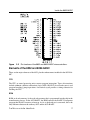
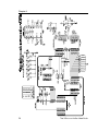
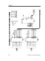
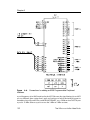
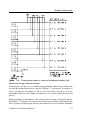
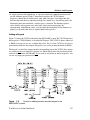
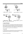
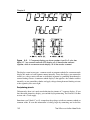
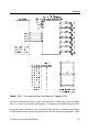
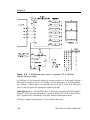
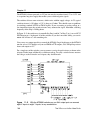
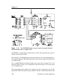
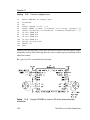
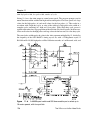
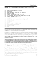
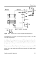
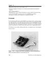
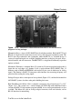
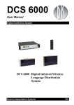
1
You download this file from web-site: http://www.pcports.ru
The
Microcontroller Idea Book
Circuits, Programs, & Applications
featuring the 8052-BASIC Microcontroller
Jan Axelson
Lakeview Research
Madison, WI
copyright 1994, 1997 by Jan Axelson
Published by Lakeview Research
14 13 12 11 10 9 8 7 6 5 4
Lakeview Research
5310 Chinook Ln.
Madison, WI 53704
USA
Phone: 608-241-5824
Fax: 608-241-5848
Email: [email protected]
WWW: http://www/lvr.com
No part of this book, except the programs and program listings, may be reproduced in any
form, or stored in a database or retrieval system, or transmitted or distributed in any form,
by any means, electronic, mechanical photocopying, recording, or otherwise, without the
prior written permission of Lakeview Research or the author, except as permitted by the
Copyright Act of 1976. The programs and program listings, or any portion of these, may be
stored and executed in a computer system and may be incorporated into computer programs
developed by the reader.
Trademarks
Macintosh is a registered trademark of Apple Computer. Procomm Plus and Datastorm are
registered trademarks of Datastorm Technologies, Inc. VT100 is a registered trademark of
Digital Equipment Corporation. IBM is a registered trademark of International Business
Machines Corporation. MCS-BASIC-52 and Intel are registered trademarks of Intel Corporation. Microsoft, MS-DOS, GW-BASIC, and Microsoft Windows are registered trademarks
of Microsoft Corporation. Philips is a registered trademark of Philips International BV.
The author and publisher have used their best efforts in preparing this book and the
materials in it. The author built and tested the electronic circuits described, ran and tested
the computer programs presented, and reviewed all materials for completeness and
accuracy. The author and publisher make no warranty with regard to the circuit
schematics, program listings, and other materials in this book. The author and publisher
take no responsibility for any damages resulting from any use of the material in this book.
ISBN 0-9650819-4-X
Apart from any fair dealing for the purposes of research or private study, or criticism or review, as permitted under the relevant copyright,
designs and patents acts, this publication may only be reproduced, stored or transmitted, in any form or by any means, with the prior
permission in writing of the publisher. eBooks Corporation
Table of Contents
Chapter 1
Microcontroller Basics
What’s a Microcontroller? 1
A Little History 2
New Tools 3
Project Steps 4
1
Chapter 2
Inside the 8052-BASIC
Possibilities 11
Limits 13
What You Need 14
The 8051 Family 16
Elements of the 8052 and 8052-BASIC 17
11
Chapter 3
Powering Up
About the Circuit 23
Circuit Construction 30
Powering Up 35
Basic Tests 38
Simple Programs to Try 40
Exiting Programs 44
23
Chapter 4
Saving Programs
Nonvolatile Memory Options 47
Adding NVRAM or EEPROM 50
Using the Programming Commands 53
Adding Bootup Options 54
47
iii
Erasing NV Memory 55
Adding more NVRAM or EEPROM 56
Adding EPROM 56
EPROM-programming Circuits 57
Power Supplies for Programming 61
Storing Programs on Disk 63
Chapter 5
Programming
Programming Basics 65
BASIC-52 Bugs and Things to Watch Out For 69
Finding Program Errors 70
BASIC-52 Keywords by Function 72
Quick Reference to BASIC-52 74
65
Chapter 6
Inputs and Outputs
The Memory Map 87
Uses for I/O Ports 89
Adding Ports 89
The 8255 Programmable Peripheral Interface 98
87
Chapter 7
Switches and Keypads
Simple Switches 109
Adding a Keypad 116
109
Chapter 8
Displays
Using LEDs 125
7-segment Displays 129
Displaying Messages 138
Inside the Display Controller 140
Mounting Displays in an Enclosure 152
125
Chapter 9
Using Sensors to Detect and Measure
Sensor Basics 153
Choosing Sensors 154
On/off Sensors 155
Analog Sensors 156
Sensor Examples 163
Level Translating 167
Choosing a Converter 169
153
Chapter 10
Clocks and Calendars
BASIC-52’s Real-time Clock 171
A Watchdog Timekeeper 174
171
iv
Chapter 11
Control Circuits
Switching Power to a Load 185
Controlling a Switch Matrix 187
Op Amp with Programmable Gain 189
Controlling a Stepper Motor 191
Speed Control of a Continuous DC Motor 195
185
Chapter 12
Wireless Links
Infrared Links 199
Increasing the Distance 212
Radio Links 216
199
Chapter 13
Calling Assembly-language Routines
Assembly-language Basics 218
What You Need 218
Loading a Routine 221
File Formats for Assembly-language Routines 222
Assembling a Program 224
Uploading a Program 225
Example: Creating a Sine Wave 227
Avoiding Program Crashes 231
Interrupts 232
Adding Custom Commands and Instructions 233
A General-purpose EPROM Programmer 237
217
Chapter 14
Running BASIC-52 from External Memory
Reasons 239
Copying BASIC-52 240
System Requirements 241
Storing BASIC-52 Programs 243
239
Chapter 15
Related Products
Enhanced BASIC-52 245
BASIC Compilers 246
Programming Environments 247
Pc Boards 248
BASIC-52 Source Code 250
245
Appendix A Sources
Books 251
BBS’s 254
Product Vendors 255
251
v
Appendix B Programs for Loading Files
263
Appendix C Number Systems
About Number Systems 271
Kilobytes and Megabytes 273
271
vi
Introduction
Introduction
This book is a hands-on guide to designing, building, and testing microcontroller-based
devices. Microcontrollers, or single-chip computers, are ideal for projects that require
computer intelligence, but don’t need the overhead of a complete personal computer with
disk drives, keyboard, and full-screen display.
Why the 8052-BASIC?
This book focuses on the 8052-BASIC microcontroller, which is easy to use, full featured,
and inexpensive to work with. The on-chip BASIC-52 programming language enables you
to write, run, and test your programs quickly. With over 100 commands, instructions, and
operators, BASIC-52 is more capable than other microcontroller BASICs. And, as a member
of the 8051 microcontroller family, the 8052-BASIC has a standard, popular architecture.
The ideas and applications presented here are not limited to the 8052-BASIC, however. If
your favorite chip is a different one, you can adapt the circuits and programs to it. The
schematics and program listings in this book include comments and explanations to help
you apply the ideas, whether or not you are using the 8052-BASIC.
vii
Introduction
What’s Inside?
This is not just a textbook that presents information but glosses over the details of how to
apply it. Inside, you’ll find practical information, including the following:
• Complete circuit schematics and parts lists—so you can easily build the circuits
yourself.
• Design theory—for example, why use this particular component? or how can I expand
or modify the circuit shown?
• Example program listings—for easy testing and use of the circuits.
• Construction and debugging tips—to help you get the circuits up and running without
problems.
The appendices include a complete list of sources to help you find the components and
additional information you need for your projects.
Because microcontroller projects involve both circuit design and programming, I cover both
the hardware and software aspects. The book begins with an introduction to microcontrollers, and to the 8052-BASIC chip in particular. Next are basic circuits to get you started
programming and interfacing to the chip, along with the reasons behind the component and
design choices, and construction details for prototyping. To the basic circuits, I show how
to add switches, keypads, displays, and other input/output interfaces.
A programming reference describes each of BASIC-52’s keywords, with specific tips for
trouble-free programming in BASIC-52.
You’ll also find out how to add these to your system:
• Sensors, for detecting detect and measuring physical properties.
• Clock/calendar functions, for keeping track of seconds, minutes, hours, days, months,
and years, and to trigger alarms at particular times.
• Control of AC power, switch matrices, stepper and continuous motors, and gain of an
op amp.
• Programmable wireless links, for situations where stringing wires isn’t practical or
convenient.
viii
Introduction
A chapter on assembly-language interfacing shows how to add assembly-language programs
for faster program execution, how to add your own commands the BASIC-52 programming
language, and how to use the 8052-BASIC as a development system for an all-assemblylanguage project.
The final chapters cover other options for 8052-BASIC systems, including how to store
BASIC-52 in external memory rather than in the 8052’s internal ROM, and a review of
related products, including BASIC compilers, 8052-BASIC circuit boards, and development
software for more convenient and possibly cheaper project development.
Your Feedback Is Welcome
This book is the result of requests from readers of my articles in ComputerCraft magazine
and its successor, The MicroComputer Journal. I’ve expanded the coverage of several topics,
including programming of EPROMs and other devices, display options, sensors, and
programming tips.
Thanks to everyone who responded to my articles with comments, questions, criticisms, and
suggestions, and who, in doing so, helped to make this book as useful as it can be. As always,
I welcome your comments on this work.
Jan Axelson
10-94
ix
x
Microcontroller Basics
1
Microcontroller Basics
This chapter introduces you to the world of microcontrollers, including definitions, some
history, and a summary of what’s involved in designing and building a microcontroller
project.
What’s a Microcontroller?
A microcontroller is a computer-on-a-chip, or, if you prefer, a single-chip computer. Micro
suggests that the device is small, and controller tells you that the device might be used to
control objects, processes, or events. Another term to describe a microcontroller is embedded
controller, because the microcontroller and its support circuits are often built into, or
embedded in, the devices they control.
You can find microcontrollers in all kinds of things these days. Any device that measures,
stores, controls, calculates, or displays information is a candidate for putting a microcontroller inside. The largest single use for microcontrollers is in automobiles—just about every
car manufactured today includes at least one microcontroller for engine control, and often
more to control additional systems in the car. In desktop computers, you can find microcontrollers inside keyboards, modems, printers, and other peripherals. In test equipment,
microcontrollers make it easy to add features such as the ability to store measurements, to
create and store user routines, and to display messages and waveforms. Consumer products
that use microcontrollers include cameras, video recorders, compact-disk players, and
ovens. And these are just a few examples.
The Microcontroller Idea Book
1
Chapter 1
A microcontroller is similar to the microprocessor inside a personal computer. Examples of
microprocessors include Intel’s 8086, Motorola’s 68000, and Zilog’s Z80. Both microprocessors and microcontrollers contain a central processing unit, or CPU. The CPU executes
instructions that perform the basic logic, math, and data-moving functions of a computer.
To make a complete computer, a microprocessor requires memory for storing data and
programs, and input/output (I/O) interfaces for connecting external devices like keyboards
and displays.
In contrast, a microcontroller is a single-chip computer because it contains memory and I/O
interfaces in addition to the CPU. Because the amount of memory and interfaces that can fit
on a single chip is limited, microcontrollers tend to be used in smaller systems that require
little more than the microcontroller and a few support components. Examples of popular
microcontrollers are Intel’s 8052 (including the 8052-BASIC, which is the focus of this
book), Motorola’s 68HC11, and Zilog’s Z8.
A Little History
To understand how microcontrollers fit into the always-expanding world of computers, we
need to look back to the roots of microcomputing.
In its January 1975 issue, Popular Electronics magazine featured an article describing the
Altair 8800 computer, which was the first microcomputer that hobbyists could build and
program themselves. The basic Altair included no keyboard, video display, disk drives, or
other elements we now think of as essential elements of a personal computer. Its 8080
microprocessor was programmed by flipping toggle switches on the front panel. Standard
RAM was 256 bytes and a kit version cost $397 ($498 assembled). A breakthrough in the
Altair’s usability occurred when a small company called Microsoft offered a version of the
BASIC programming language for it.
Of course, the computer world has changed a lot since the introduction of the Altair.
Microsoft has become an enormous software publisher, and a typical personal computer
now includes a keyboard, video display, disk drives, and Megabytes of RAM. What’s more,
there’s no longer any need to build a personal computer from scratch, since mass production
has drastically lowered the price of assembled systems. At most, building a personal
computer now involves only installing assembled boards and other major components in an
enclosure.
A personal computer like Apple’s Macintosh or IBM’s PC is a general-purpose machine,
since you can use it for many applications—word processing, spreadsheets, computer-aided
design, and more—just by loading the appropriate software from disk into memory.
Interfaces to personal computers are for the most part standard ones like those to video
displays, keyboards, and printers.
2
The Microcontroller Idea Book
Microcontroller Basics
But along with cheap, powerful, and versatile personal computers has developed a new
interest in small, customized computers for specific uses. Each of these small computers is
dedicated to one task, or a set of closely related tasks. Adding computer power to a device
can enable it to do more, or do it faster, better, or more cheaply. For example, automobile
engine controllers have helped to reduce harmful exhaust emissions. And microcontrollers
inside computer modems have made it easy to add features and abilities beyond the basic
computer-to-phone-line interface.
In addition to their use in mass-produced products like these, it’s also become feasible to
design computer power into one-of-a-kind projects, such as an environmental controller for
a scientific study or an intelligent test fixture that ensures that a product meets its specifications before it’s shipped to a customer.
At the core of many of these specialized computers is a microcontroller. The computer’s
program is typically stored permanently in semiconductor memory such as ROM or
EPROM. The interfaces between the microcontroller and the outside world vary with the
application, and may include a small display, a keypad or switches, sensors, relays, motors,
and so on.
These small, special-purpose computers are sometimes called single-board computers, or
SBCs. The term can be misleading, however, since the computer doesn’t have to be on a
single circuit board, and many types of computer systems, such as laptop and notebook
computers, are now manufactured on a single board.
New Tools
To design and build a computer-controlled device, you need skills in both circuit design and
software programming. The good news is that a couple of recent advances have simplified
the tasks involved.
One is the introduction of microcontrollers themselves, since they contain all of the elements
of a computer on a single chip. Using a microcontroller can reduce the number of
components and thus the amount of design work and wiring required for a project. The
8052-BASIC microcontroller even includes its own programming language, called BASIC52.
The other development is personal computers themselves. A desktop computer can help
tremendously by serving as a host system for writing and testing programs. As you are
developing a project, you can use a serial link to connect the host system to a target system,
which contains the microcontroller circuits you are testing. You can then use the personal
computer’s keyboard, video display, disk drives, and other resources for writing and testing
programs and transferring files between the two systems.
The Microcontroller Idea Book
3
Chapter 1
Project Steps
Putting together a microcontroller project involves several steps:
1. Define the task
2. Design and build the circuits
3. Write the control program
4. Test and debug
Sometimes the steps won’t follow exactly in this order. You may begin writing your program
before you build the circuits, or you may build and test some of the circuits before you start
programming. But however you go about it, each of the above steps is part of the process.
To see what’s involved in each step, let’s look at each in more detail.
Defining the Task
Every project begins with an idea, or a problem that needs a solution. For example, How
can I monitor light intensity at different locations and times of day to find the best location
for a solar collector? Or how can I automate the process of drilling printed-circuit boards?
Or how can I create a computer-controlled, animated display for a store window?
Once you know what you want to accomplish, you need to determine whether or not your
idea is one that requires a computer at all. In general, a computer is the way to go when the
circuits must make complex decisions or deal with complex data. For example, a simple
AND gate can easily decide whether or not two inputs are both valid logic highs, and will
change its output accordingly. But it would require many small-scale chips to build a circuit
that stores a series of values representing sensor outputs and the times they occurred, and
displays the information in an easily understandable form.
This type of application is where microcontrollers come in handy. Inside, microcontrollers
are little more than a carefully designed array of logic gates and memory cells, but modern
fabrication processes allow thousands of these to fit on a single chip. Since the basic
functions of a microcontroller—performing arithmetic, logic, data-moving, and program
branching functions—are common ones that are useful in many applications, it’s practical
to design and market a chip that performs these functions. The user accesses the abilities of
the microcontroller by writing a program that performs the desired functions.
On the other end of the scale, how do you know if an idea is suitable for a microcontroller,
or whether you should use a full desktop computer? If your design requires users to enter
or view complex commands, data, or graphical information, or if you need large amounts
of data or program storage, then a system with keyboard, full-screen display, and disk drives
4
The Microcontroller Idea Book
Microcontroller Basics
makes sense. For simpler designs, a microcontroller with perhaps a keypad, small display,
and solid-state memory (no disk drives) can often do the job, with less expense and smaller
size.
In fact, recently the two extremes have been meeting. Some 32-bit microcontrollers are as
capable as desktop systems, and notebook-size computers are available with solid-state,
diskless storage. Also, expansion cards, other hardware, and software are now available for
those who want to use desktop computers for monitoring and control tasks. So there’s
something for everyone.
The 8052-BASIC chip described in this book is perfect for many simpler applications,
especially control and monitoring tasks. Because the chip is easy to use, it’s a good way to
learn about microcontrollers and computers in general. Although you can’t do the most
complex projects with it, you can do a lot, at low cost and without a lot of hassle.
Designing and Building
When you’re ready to design and build the circuits for a project, there are several ways to
proceed. You can design your circuits from scratch, using manufacturers’ data books as
guides; you can follow a tested design (a kit or project presented in a magazine for example);
or you can buy an assembled single-board computer, adding only the interfaces and
programming your application requires. This book presents designs that you can build
yourself, but you can also use a kit or assembled board as a base if you wish.
Choosing a chip. Does it matter which microcontroller chip you use? All microcontrollers
contain a CPU, and chances are that you can use any of several devices for a specific project.
Within each device family, you’ll usually find a selection of family members, each with
different combinations of options. For example, the 8052-BASIC is a member of the 8051
family of microcontrollers, which includes chips with program memory in ROM or EPROM,
and with varying amounts of RAM and other features. You select the version that best suits
your system’s requirements.
Microcontrollers are also characterized by how many bits of data they process at once, with
a higher number of bits generally indicating a faster or more powerful chip. Eight-bit chips
are popular for simpler designs, but 4-bit, 16-bit, and 32-bit architectures are also available.
The 8052-BASIC is an 8-bit chip.
Power consumption is another consideration, especially for battery-powered systems. Chips
manufactured with CMOS processes usually have lower power consumption than those
manufactured with NMOS processes. Many CMOS devices have special standby or “sleep”
modes that limit current consumption to as low as a few microamperes when the circuits are
The Microcontroller Idea Book
5
Chapter 1
inactive. Using these modes, a data logger can reduce its power consumption between
samples, and power up only when it’s time to take data.
The 8052-BASIC chip is available in both NMOS and CMOS versions. The original
8052-BASIC was an NMOS chip, offered directly from Intel. (Intel’s term for its NMOS
process is HMOS.) Although Intel never offered a CMOS version directly, Micromint
became a source by ordering a batch of CMOS 8052’s with the BASIC-52 programming
language in ROM. The CMOS version, the 80C52-BASIC, has maximum power consumption of 30 milliamperes, compared to 175 milliamperes for the NMOS 8052-BASIC.
All microcontrollers have a defined instruction set, which consists of the binary words that
cause the CPU to carry out specific operations. For example, the instruction 0010 0110 tells
an 8052 to add the values in two locations. The binary instructions are also known as
operation codes, or opcodes for short. The opcodes perform basic functions like adding,
subtracting, logic operations, moving and copying data, and controlling program branching.
Control circuits often require reading or changing single bits of input or output, rather than
reading and writing a byte at a time. For example, a microcontroller might use the eight bits
of an output port to switch power to eight sockets. If each socket must operate independently
of the others, a way is needed to change each bit without affecting the others. Many
microcontrollers include bit-manipulation (also called Boolean) opcodes that easily allow
programs to set, clear, compare, copy, or perform other logic operations on single bits of
data, rather than a byte at a time.
Options for storing programs. Another consideration in circuit design is how to store
programs. Instead of using disk storage, most microcontroller circuits store their programs
on-chip. For one-of-kind projects or small-volume production, EPROM has long been the
most popular method of program storage. Besides EPROMs, other options include
EEPROM, ROM, nonvolatile (NV), or battery-backed, RAM, and Flash EPROM. The
program memory may be in the microcontroller chip, or a separate component.
To save a program in EPROM, you must set the EPROM’s data and address pins to the
appropriate logic levels for each address and apply special programming voltages and
control signals to store the data at the selected address. The programming process is
sometimes called burning the EPROM. You erase the contents by exposing the chip’s quartz
window, and the circuits beneath it, to ultraviolet energy.
Some microcontrollers contain a one-time-programmable, or field-programmable, EPROM.
This type has no window, so you can’t erase its contents, but because it’s cheaper than a
windowed IC, it’s a good choice when a program is finished and the device is ready for
quantity production.
6
The Microcontroller Idea Book
Microcontroller Basics
Several techniques are available for programming EPROMs and other memory chips. With
a manual programmer, you flip switches to toggle each bit and program the EPROM byte
by byte. This is acceptable for short programs, but quickly becomes tedious with a program
of any length. Computer control simplifies the job greatly. With an EPROM programmer
that connects to a personal computer, you can write a program at your keyboard, save it to
disk if you wish, and store the program in EPROM in a few easy steps. Data sheets for
EPROMs rarely specify the number of erase and reprogramming cycles a device is
guaranteed for, but a typical EPROM should endure 100 erase/program cycles, and usually
many more.
EEPROMs are much like EPROMs except that they are electrically erasable—no ultraviolet
source is required. Limitations of EEPROMs include slow speed, high cost, and a limited
number of times that they can be reprogrammed (typically 10,000 to 100,000).
ROMs are cost-effective when you need thousands of copies of a single program. ROMs
must be factory-programmed and once programmed, can’t be changed.
NVRAM typically includes a lithium cell, control circuits, and RAM encapsulated in a
single IC package. When power is removed from the circuit, the lithium cell takes over and
preserves the information in RAM, for 10 years or more. You can reprogram an NVRAM
n infinite number of times, with the only limitation being battery life.
Flash EPROM is electrically erasable, like EEPROM, but most Flash devices erase all at
once, or in a few large blocks, rather than byte-by-byte like EEPROM. Some Flash EPROMs
require special programming voltages. As with EPROMs, the number of erase/program
cycles is limited.
The 8052-BASIC uses two types of program memory. An 8-kilobyte, or 8K, on-chip ROM
stores the BASIC-52 interpreter. For storing the BASIC-52 programs that you write, the
BASIC-52 language has programming commands that enable you to save programs in
external EPROM, EEPROM, or NVRAM.
Other memory. Most systems also require a way to store data for temporary use. Usually,
this is RAM, whose contents you can change as often as you wish. Unlike EPROM, ROM,
EEPROM, and NVRAM, the contents of the RAM disappear when you remove power the
chip (unless it has battery back-up).
Most microcontrollers include some RAM, typically a few hundred bytes. The 8052-BASIC
has 256 bytes of internal RAM. A complete 8052-BASIC system requires at least 1024 bytes
of external RAM as well.
I/O options. Finally, input/output (I/O) requires design decisions. Most systems require
interfaces to things like sensors, keypads, switches, relays, and displays. Most microconThe Microcontroller Idea Book
7
Chapter 1
trollers have ports for interfacing to the world outside the chip. The 8052-BASIC uses many
of its ports for accessing external memory and performing other special functions, but some
port bits are available for user applications, and you can easily increase the available I/O by
adding support chips.
Writing the Control Program
When it’s time to write the program that controls your project, the options include using
machine code, assembly language, or a higher-level language. Which programming language you use depends on things like desired execution speed, program length, and
convenience, as well as what’s available in your price range.
Machine code. The most fundamental program form is machine code, the binary instructions that cause the CPU to perform the operations you desire.
Assembly language. One step removed from machine code is assembly language, where
abbreviations called mnemonics (memory aids) substitute for the machine codes. The
mnemonics are easier to remember than the machine codes they stand for. For example, in
the 8052’s assembly language, the mnemonic CLR C means clear the carry bit, and is easier
to remember than its binary code (11000011).
Since machine code is ultimately the only language that a CPU understands, you need some
way of translating assembly-language programs into machine code. For very short programs,
you can hand assemble, or translate the mnemonics yourself by looking up the machine
codes for each abbreviation. Another option is to use an assembler, which is software that
runs on a desktop computer and translates the mnemonics into machine code. Most
assemblers provide other features, such as formatting the program code and creating a listing
that shows both the machine-code and assembly-language versions of a program side
-by-side.
Higher-level languages. A disadvantage to assembly language is that each device family
has its own set of mnemonics, so you have to learn a new vocabulary for each family you
work with. To get around this problem, higher-level languages like C, Pascal, Fortran, Forth,
and BASIC follow a standard syntax so that programs are more portable from one device
to another. The idea is that with minor changes, you can use a language like BASIC to write
programs for many different devices. In reality, each language tends to develop many
different dialects, depending on the chip and the preferences of the language’s vendor, so
porting a program to a different device isn’t always effortless. But there are many similarities
among the dialects of a single language, so, as with spoken language, a new dialect is easier
to learn than a whole new language.
Higher-level languages also simplify programming by allowing you to do in one or a few
lines what would require many lines of assembly code to accomplish.
8
The Microcontroller Idea Book
Microcontroller Basics
Interpreters and compilers are two forms of higher-level languages. An interpreter translates a program into machine code each time the program runs, while a compiler translates
only once, creating a new, executable file that the computer runs directly, without re-translating.
As a rule, interpreters are very convenient for shorter programs where execution speed isn’t
critical. With an interpreted language, you can run your program code immediately after you
write it, without a separate compile or assembly step. A compiler is a good choice when a
program is long or has to execute quickly. A single language like BASIC may be available
in both interpreted and compiled versions.
Each device family requires its own interpreter or compiler to translate the higher-level code
into the machine code for that device. In other words, you can’t use QuickBASIC for IBM
PCs to program an 8052 microcontroller—you need a compiler that generates program code
for the 8052.
Compared to an equivalent program written in assembly language, a compiled program
usually is larger and slower, so assembly language is the way to go if a program must be as
fast or as small as possible. A higher-level language also may not offer all of the abilities of
assembly code, though you can get around this by calling subroutines in assembly language
when necessary.
BASIC-52 is an interpreted language, but BASIC compilers for the 8052 are also available.
In fact, you can have the best of both worlds by testing your programs with the BASIC-52
interpreter, and compiling the finished product for faster execution and other benefits of the
compiled version.
Testing and Debugging
After you’ve written a program, or a section of one, it’s time to test it and as necessary, find
and correct mistakes to get it working properly. The process of ferreting out and correcting
mistakes is called debugging. Easy debugging and troubleshooting can make a big difference
in how long it takes to get a system up and running. As with programming, you have several
options here as well.
Testing in EPROM. One way is to burn your program into EPROM, install the EPROM
in your system, run the program, and observe the results. If problems occur (as they usually
will) you modify the program, erase and reburn the EPROM, and try again, repeating as
many times as necessary until the system is operating properly.
Development systems. Another option is to use a development system. A typical development system consists of a monitor program, which is a program stored in EPROM or other
memory in the microcontroller system, and a serial link to a personal computer. Using the
The Microcontroller Idea Book
9
Chapter 1
abilities of the monitor program, you can load your program from a personal computer into
RAM (instead of the more permanent EPROM) on the microcontroller system, then run the
program, modify it, and retry as often as necessary until the program is working properly.
Most development systems also allow single-stepping, setting breakpoints, and viewing and
changing the data in memory. In single-stepping, you run the program one step at time,
pausing after each step, so you can more easily monitor what the circuits and program are
doing at each step. A breakpoint is a program location where the program stops executing
and waits for a command to continue. You can set breakpoints at critical spots in your
program. At any breakpoint, you can view or change the contents of memory or perform
other tests.
Simulators. Another development tool is a simulator, which is software that runs on a
desktop computer and uses the video display to demonstrate what would happen if a specific
microprocessor or microcontroller were to run a particular program. You can look “inside”
the simulated chip, observe the contents of internal memory, and single-step or set breakpoints to stop program execution at a desired program location or condition. In this way,
you can get a program working properly before you commit it to EPROM. One drawback
to simulators is that they can’t mimic all features of the chip of interest, especially
interrupt-response and timing characteristics.
Emulators. An in-circuit emulator (ICE) is hardware that replaces the microprocessor in
question by plugging into the microprocessor’s socket on the device you want to test. Like
a simulator, an emulator lets you control program execution and monitor what happens at
each program step. Microprocessor emulators typically are expensive. A ROM emulator is
a lower-cost option that simulates an EPROM (using RAM, for example) for program
storage, and usually provides the abilities of a development system as well.
The 8052-BASIC’s development system. The 8052-BASIC system and a personal computer form a complete development system for writing, testing, and storing programs. The
personal computer’s keyboard and screen make it easy to write and run programs and view
the results.
BASIC-52 has many built-in debugging features that make it easy to test programs. You can
run a program immediately after writing it, without having to assemble, compile, or program
an EPROM. You can use a STOP statement and CONT (continue) command to set
breakpoints and resume executing your program. You can use PRINT statements to display
variables as the program runs. And, if you wish, you can use your personal computer for
writing programs off-line and uploading and downloading them to the 8052-BASIC system.
10
The Microcontroller Idea Book
Inside the 8052-BASIC
2
Inside the 8052-BASIC
This chapter introduces you to the 8052-BASIC chip, including the kinds of projects you
can do with it, what equipment, materials, and skills you need in order to design and build
an 8052-BASIC project, and a pin-by-pin look at the chip and its abilities.
Possibilities
The 8052-BASIC microcontroller is an easy-to-use, low-cost, and versatile computer-on-achip. It’s ideal for projects that require more than an assortment of logic gates, but less than
a complete desktop computer system with a full keyboard, display, and disk drives. If you’re
interested in doing more with computers than simply running applications programs, the
8052-BASIC gives you a chance to design and build a system from the ground up.
With a few support chips and a program stored in memory, you can use the 8052-BASIC to
sense, measure, and control processes, events, or conditions. Here are just a few examples
of the uses you can put it to:
• data collection
• machine control
• test equipment
• wired and wireless links for communications and control
The Microcontroller Idea Book
11
Chapter 2
The 8052-BASIC is actually two products in one: it’s an 8052 microcontroller, with the
BASIC-52 programming language on-chip. To begin using the 8052-BASIC, you need a
minimum circuit consisting of the 8052-BASIC and some support components, plus a
personal computer. This book contains specific instructions for use with “IBM-compatible,”
or MS-DOS, computers, but you can use any computer that has an RS-232 serial port and
communications software to go with it. Figure 2-1 shows the basic setup.
With an 8052-BASIC circuit connected by a serial link to a personal computer, you have a
complete development system with these abilities:
• You can write and run BASIC programs. You use the keyboard, video display, and
other resources of the personal computer to type and view the programs and commands
that the 8052-BASIC system executes. BASIC-52 is an interpreted language whose
programs do not require an additional assembling or compiling step. You can run
programs or execute commands immediately after you write them.
• You can use BASIC-52’s programming functions to permanently store your programs
in EPROM or other nonvolatile memory. You don’t need a separate EPROM
programmer.
Figure 2-1 Setup for working with the 8052-BASIC.
12
The Microcontroller Idea Book
Inside the 8052-BASIC
• You can also store programs on your personal computer’s disk. You can write or edit
programs on your personal computer, and then upload them to the 8052-BASIC system.
• To the basic circuits, you can add displays, switches, keypads, relays, and other
components, depending on the needs of your project.
• After program development, you can disconnect the link to the personal computer and
let the 8052-BASIC system run its stored program on its own.
Limits
No single product is ideal for every use. These are some of the limitations to the 8052-BASIC:
• Program execution can be slow, compared with programs that run on more powerful
computers, or programs written in assembly language. A typical program line in
BASIC-52 takes several milliseconds to execute. Because of this, there are some tasks
that BASIC-52 just can’t handle—for example, detecting and responding to an interrupt
within a few microseconds. But for many control, monitoring, and other tasks,
BASIC-52 is fine. For example, a weather station that senses conditions once per
minute and stores or displays the results doesn’t need super-fast response. And, if
necessary, you can call an assembly-language routine for a portion of a program where
speed is critical.
Even if you write your programs in assembly language, C, or another language, you can
use the 8052-BASIC system as a development system that enables you to upload your
program to memory, run the program, and test and debug your programs and circuits.
• Another limitation of the 8052-BASIC is that a complete project requires additional
components. If you’re looking for a true single-chip solution, the 8052-BASIC isn’t it.
Even a minimal system requires an external RAM chip, and most systems also have an
external EPROM or other non-volatile memory. The serial link and other optional
functions also use some of the on-chip timers and input/output ports, so these may not
be available for other uses.
Still, the 8052-BASIC lets you to do a lot with a little. When needed, you can easily add
chips to expand the input/output ports, timers, and other functions.
• And finally, don’t expect BASIC-52 to have the abilities of QBasic, Visual Basic or
other BASIC programming languages that you may use on your personal computer.
BASIC-52 is more capable than many other single-chip BASICs. It includes features
like loops, subroutines, string handling, and even floating-point math for handling
The Microcontroller Idea Book
13
Chapter 2
fractional quantities. But there are some primitive aspects to the language. For example,
the on-line editing functions are limited. Once you write a program line, you can
change it only by retyping from the beginning. The limitations are understandable,
because the entire programming language has to fit in the 8052’s 8 kilobytes of ROM.
Fancy editing and other features just aren’t feasible in this small space.
There are solutions here as well. You can get around many of the editing limitations by
writing and editing programs off-line, using your personal computer and text editor, and
then uploading to the 8052-BASIC system. And, there are software and hardware
products that enhance BASIC-52 and make it easier to use, especially for longer, more
complex programming jobs.
What You Need
To use the 8052-BASIC chip, you need the following equipment, materials, and skills:
Components
The 8052-BASIC chip and supporting components are widely available. Appendix A lists
sources for the components used in the circuits described in this book.
Power Supply
You’ll need a regulated +5-volt power supply to power the circuits. Output capability of at
least 500 milliamperes is recommended for general experimenting. The power supply can
be powered by batteries or AC line voltage, but it must have a regulated output between 4.75
and 5.25 volts.
Construction Materials
To build the circuits, you’ll need circuit-construction materials and the skills to use them.
Wire-wrapping is an effective, quick way to build the circuits described, but if you prefer,
you can use point-to-point soldering or design and make a printed-circuit board, or use any
method that you’re comfortable with. Another option is to buy one of the available kits or
prebuilt 8052-BASIC boards. You can then use this book as a guide to using and expanding
the abilities of your board. Appendix A lists board suppliers and books on project-construction techniques.
Documentation
Using just the information in this book, you can build and begin using your system. For
serious experimenting, two additional references are recommended: programming and
14
The Microcontroller Idea Book
Inside the 8052-BASIC
hardware manuals. For programming, you have two choices: Intel’s BASIC-52 User’s
Manual, or Systronix’s BASIC-52 Programming. Each of these describes the BASIC-52
programming language in detail. The Intel manual includes a few schematics, while
Systronix’s version has more programming examples and is better organized in general.
Intel’s Embedded Microcontrollers data book is a hardware reference that describes the 8052
chip, including electrical specifications and timing requirements. It also includes an assembly-language reference. Appendix A tells where to get these.
Other useful documentation includes data sheets for the other components in your projects.
For a small charge, many component vendors will send along data sheets for the parts you
order.
Host Computer
To program the 8052-BASIC, you connect its circuits to a host computer, using an RS-232
asynchronous serial port and terminal-emulation software. The computer can be any type,
as long as it has a serial port and appropriate software.
The serial port is the same connector where you plug in an external modem, serial printer,
serial mouse, or other RS-232 serial device.
Terminal-emulation software is the same type of software that you may use for modem
communications with an on-line BBS. Examples for MS-DOS computers are Datastorm
Table
Chip
2-1.
Differences among 8051-family chips.
Program Memory
Ram
(bytes)
Timers
Type
kilobytes
8051
ROM
4
128
2
8052
ROM
8
256
3
8031
none
-
128
2
8032
none
-
256
3
8751
EPROM
4
128
2
8752
EPROM
8
256
3
• 80C51, 80C52, 80C31, and so on are CMOS versions of above.
• 80C51FA/B/C add more versatile timers and an enhanced serial channel.
• 8052-BASIC has the BASIC-52 programming language in ROM.
• Packages include 40-pin DIP, 40-lead PLCC, and 44-pin QFP.
The Microcontroller Idea Book
15
Chapter 2
Technologies’ Procomm Plus and the Terminal accessory in Microsoft Windows. At minimum, the software must enable you to do the following: set the baud rate and other
communications parameters, serially transmit the characters that you type at the keyboard,
and display the characters received at the serial port. Also useful, but not essential, is the
ability to upload and download text files from your disk, over the serial link. If you don’t
have a favorite communications program, look in shareware catalogs or the file areas of
online services or BBS’s, where you can try out the offerings for a small disk-copying or
downloading charge.
Test Equipment
Some basic test equipment will help you monitor, test, and troubleshoot your circuits.
Minimum requirements include a multimeter capable of reading volts, ohms, and milliamperes. Just about any basic meter will do for this. A logic probe is convenient, but not
essential, for monitoring logic levels and transitions. Best of all, an oscilloscope lets you
view the actual waveforms on one or more channels.
Knowledge
This book assumes that you have a basic knowledge of electronic circuits, including digital
logic. It does not assume that you know a lot about computer programming and computer
circuits. Appendix A lists some books that cover the basics, if you want to review or learn
these. Appendix C is a review of hexadecimal, binary, and decimal number systems.
The 8051 Family
At the core of the 8052-BASIC is an 8052 microcontroller, a member of the 8051
microcontroller family. Intel Corporation introduced the 8051 in 1980. Since that time,
8051-family chips have been used as the base of thousands of products. Many other
companies, including Philips, Siemens, Dallas Semiconductor, OKI, Fujitsu, and HarrisMatra now also make 8051-family chips. Some companies have expanded the 8051 family
by offering compatible chips with additional features.
Table 2-1 summarizes the differences among popular 8051-family chips. The 8052 is an
enhanced 8051, with an extra timer and more RAM and ROM. The 8031 and 8032 are
identical to the 8051 and 8052, except that the ROM area is unused, and program code must
be stored in an external EPROM or other memory chip.
The 8052, like other 8051-family chips, is available in NMOS and CMOS versions. Figure
2-2 shows the pinout of the 8052 and 8052-BASIC, and Table 2-2 describes the pin
functions.
16
The Microcontroller Idea Book
Inside the 8052-BASIC
Figure
2-2 Pin functions of the 8052 and 8052-BASIC microcontrollers.
Elements of the 8052 and 8052-BASIC
These are the major elements of the 8052, plus the enhancements included in the 8052-BASIC:
CPU
The CPU, or central processing unit, executes program instructions. Types of instructions
include arithmetic (addition, subtraction), logic (AND, OR, NOT), data transfer (move), and
program branching (jump) operations. An external crystal provides a timing reference for
clocking the CPU.
ROM
ROM (read-only memory) is the read-only memory that is programmed into the chip in the
manufacturing process. In the 8052-BASIC, the ROM contains the BASIC-52 interpreter
program that the 8052 executes on boot-up. As far as the hardware is concerned, this is the
only difference between the ordinary 8052 and the 8052-BASIC.
The Microcontroller Idea Book
17
Chapter 2
Table 2-2. (page 1 of 2) Pin functions of the 8052 microcontroller and
8052-BASIC additions.
Pin
Symbol
Input/
Output
8052
Function
8052-BASIC Additions
Symbol
Function
1
P1.0
T2
I/O
Port 1, bit 0;
Timer 2 external input
2
P1.1
T2(EX)
I/O
Port 1, bit 1;
Timer 2 external reload/capture
3
P1.2
I/O
Port 1, bit 2
PWM
Pulse-width-modulated output
4
P1.3
I/O
Port 1, bit 3
ALE DIS
Address latch disable
5
P1.4
I/O
Port 1, bit 4
PGM PLS Program pulse
6
P1.5
I/O
Port 1, bit 5
PGM EN
7
P1.6
I/O
Port 1, bit 6
DMA ACK DMA acknowledge
8
P1.7
I/O
Port 1, bit 7
LPT
Line printer out
9
Reset
Input
Reset system
10
P3.0
RXD
I/O
Port 3, bit 0
Serial receive
SER IN
Serial port in
11
P3.1
TXD
I/O
Port 3, bit 1
Serial transmit
SER OUT Serial port out
12
P3.2
INT0
I/O
Port 3, bit 2
External interrupt 0
DMA
REQ
13
P3.3
INT1
I/O
Port 3, bit 3
External interrupt 1
14
P3.4
T0
I/O
Port 3, bit 4
Timer 0 external input
15
P3.5
T1
I/O
Port 3, bit 5
Timer 1 external input
16
P3.6
WR
I/O
Port 3, bit 6
Write strobe for external
memory
17
P3.7
RD
I/O
Port 3, bit 7
Read strobe for external
memory
18
XTAL1
Input
Inverting oscillator amplifier
(crystal)
19
XTAL2
Output
Inverting oscillator amplifier
(crystal)
20
VSS
Input
Circuit ground
18
Programming voltage enable
DMA request
The Microcontroller Idea Book
Inside the 8052-BASIC
Table 2-2. (page 2 of 2)
Pin
Symbol
Input/
Output
8052
Function
21
P2.0
A8
I/O
Port 2, bit 0
Address bit 8
22
P2.1
A9
I/O
Port 2, bit 1
Address bit 9
23
P2.2
A10
I/O
Port 2, bit 2
Address bit 10
24
P2.3
A11
I/O
Port 2, bit 3
Address bit 11
25
P2.4
A12
I/O
Port 2, bit 4
Address bit 12
26
P2.5
A13
I/O
Port 2, bit 5
Address bit 13
27
P2.6
A14
I/O
Port 2, bit 6
Address bit 14
28
P2.7
A15
I/O
Port 2, bit 7
Address bit 15
29
PSEN
Output
Program store enable
Read strobe for external
program memory
30
ALE
Output
Address latch enable
31
EA
Input
External access enable for
program memory
32
P0.7
AD7
I/O
Port 0, bit 7
Address/data bit 7
33
P0.6
AD6
I/O
Port 0, bit 6
Address/data bit 6
34
P0.5
AD5
I/O
Port 0, bit 5
Address/data bit 5
35
P0.4
AD4
I/O
Port 0, bit 4
Address/data bit 4
36
P0.3
AD3
I/O
Port 0, bit 3
Address/data bit 3
37
P0.2
AD2
I/O
Port 0, bit 2
Address/data bit 2
38
P0.1
AD1
I//O
Port 0, bit 1
Address/data bit 1
39
P0.0
AD0
I/O
Port 0, bit 0
Address/data bit 0
40
Vcc
Input
Supply voltage
The Microcontroller Idea Book
8052-BASIC Additions
(none on pins 21-40)
19
Chapter 2
RAM
RAM (random-access memory) is where programs store information for temporary use.
Unlike ROM, the CPU can write to RAM as well as read it. Any information stored in RAM
is lost when power is removed from the chip. The 8052 has 256 bytes of RAM. BASIC-52
uses much of this for its own operations, with a few bytes available to users.
I/O Ports
I/O (Input/Output) Ports enable the 8052 to read and write to external memory and other
components. The 8052 has four 8-bit I/O ports (Ports 0-3). As the name suggests, the ports
can act as inputs (to be read) or outputs (to be written to). Many of the port bits have optional,
alternate functions relating to accessing external memory, using the on-chip timer/counters,
detecting external interrupts, and handling serial communications. BASIC-52 assigns
alternate functions to the remaining port bits. Some of these functions are required by
BASIC-52, while others are optional. If you don’t use an alternate function, you can use the
bit for any control, monitoring, or other purpose in your application.
Accessing external memory. The largest alternate use of the ports has to do with accessing
external memory. Although the 8052 is a single-chip computer, a complete 8052-BASIC
system requires additional components. It must have external RAM in addition to the 8052’s
internal RAM, and most systems also have EPROM, EEPROM, or battery-backed RAM
for permanent storage of BASIC-52 programs.
Accessing this external memory uses all of Ports 0 and 2, plus bits 6 and 7 of Port 3, to hold
data, addresses, and control signals for reading and writing to external memory. Data here
refers to a byte to be read or written, and may be any type of information, including program
code. The address defines the location in memory to be read or written.
During a memory access, Port 0’s eight pins (AD0-AD7) first hold the lower byte of the
address, followed by the data to be read or written. This method of carrying both addresses
and data on the same signal lines is called a multiplexed address/data bus. It’s a popular
arrangement that many devices use, since it requires fewer pins on the chip, compared to
giving each data and address line its own pin. Port 2’s eight lines hold the higher byte of the
address to be read or written to. These lines make up the high address bus (A8-A15). Together,
the 16 address lines can access 64 kilobytes (65,536 bytes) of memory, from 00000000
00000000 to 11111111 11111111 in binary, or 0000h to FFFFh in hexadecimal.
Besides pins to hold the data and addresses, the 8052 must also provide control signals to
initiate the read and write operations. Control signals include WR (write), RD (read), PSEN
(program store enable), and ALE (address latch enable). Some of the address lines may also
function as control signals that help to select a chip during a memory access.
20
The Microcontroller Idea Book
Inside the 8052-BASIC
Code and data memory. To understand the operation of the control signals, you need to
know a little about how the 8052 distinguishes between two types of memory: data and code,
or program, memory. By using different control signals for each type of memory, the 8052
can access two separate 64K areas of memory, with each addressed from 0000h to FFFFh,
and each using the same data and address lines.
The 8052 accesses code memory when it executes an assembly-language program or
subroutine. Code memory is read-only; you can’t write to it. The only instructions that access
code memory are read operations. Code memory is intended for programs or subroutines
that have been previously programmed into ROM or EPROM. The 8052 strobes, or pulses,
PSEN when it accesses external code memory. Accesses to internal code memory (the
BASIC-52 interpreter in ROM) do not use PSEN or any external control signals.
Data memory is read/write memory, usually RAM. Instructions that read data memory strobe
RD, and instructions that write to data memory strobe WR. The termdata memory may be
misleading, because it can hold any information that is accessed with instructions that strobe
RD or WR. In fact, BASIC-52 programs are stored in data memory, not code memory as you
might think. This is because the 8052 does not execute the BASIC programs directly. Instead,
the BASIC-52 interpreter program reads the BASIC programs as data and then translates
them to machine code for execution by the 8052.
If you don’t need all of the available memory space, you can combine code and data memory
in a single area. With combined memory, WR controls write operations, and PSEN and RD
are logically ANDed to create a read signal that is active when either PSEN or RD is low.
Combined data/code memory is handy if you want the flexibility to store either BASIC or
assembly-language programs in the same chip, or if you want to be able to upload
assembly-language routines into RAM for testing.
ALE is the final control signal for accessing external memory. It controls an external latch
that stores the lower address byte during memory accesses. When the 8052 reads or writes
to external memory, it places the lower address byte on AD0-AD7 and strobes ALE, which
causes the external latch to save the lower address byte for the rest of the read or write cycle.
After a short delay, the 8052 replaces the address on AD0-AD7 with the data to be written or
read.
Timers and Counters. The 8052 has three 16-bit timer/counters, which make it easy to
generate periodic signals or count signal transitions. BASIC-52 assigns optional functions
for each of the timer/counters.
Timer 0 controls a real-time clock that increments every 5 milliseconds. You can use this
clock to time events that occur at regular intervals, or as the base for clock or calendar
functions. Timer 1 has several uses in BASIC-52, including controlling a pulse-width-modulated output (PWM) (a series of pulses of programmable width and number); writing to a line
The Microcontroller Idea Book
21
Chapter 2
printer or other serial peripheral (LPT); and generating pulses for EPROM programming
(PGM PULSE). Timer 2 generates a baud rate for serial communications at SER IN and SER
OUT. These are all typical applications for timer/counters in microcontroller circuits.
If you don’t use the optional timer functions, you can program the timers for other
applications. In addition to timing functions, where the timer increments at a defined rate,
you can use the timers for event counting, where the timer increments on an external trigger
and measures the time between triggers. If you use the timers for event counting, T2, T2(EX),
T0, and T1 detect transitions to be counted.
The serial port. The 8052’s serial port automatically takes care of many of the details of
serial communications. On the transmit side, the serial port translates bytes to be sent into
serial data, including adding start and stop bits and writing the data in a timed sequence to
SER OUT. On the receive side, the serial port accepts serial data at SER IN and sets a flag to
indicate that a byte has been received. BASIC-52 uses the serial port for communicating
with a host computer.
External interrupts. INT0 and INT1 are external interrupt inputs, which detect logic levels
or transitions that interrupt the CPU and cause it to branch to a predefined program location.
BASIC-52 uses INT0 for its optional direct-memory-access (DMA) function.
Programming functions. BASIC-52’s programming commands use three additional port
bits (ALEDIS, PGM PULSE, and PGM EN) to control programming voltages and timing for
storing BASIC-52 programs in EPROM or other nonvolatile memory.
Additional Control Inputs
Two additional control inputs need to be mentioned. A logic high on RESET resets the chip
and causes it to begin executing the program that begins at 0 in code memory. In the
8052-BASIC chip, this program is the BASIC-52 interpreter. EA (external memory access)
determines whether the chip will access internal or external code memory in the area from
0 to 1FFFh. In BASIC-52 systems, EA is tied high so that the chip runs the BASIC interpreter
in internal ROM on boot-up.
Power Supply Connections
And, finally, the chip has two pins for connecting to a +5-volt DC power supply (VCC) and
ground (VSS).
That finishes our tour of the 8052-BASIC chip. We’re now ready to put together a working
system.
22
The Microcontroller Idea Book
Powering Up
3
Powering Up
This chapter presents a circuit that enables you to start using the 8052-BASIC chip. You can
write and run programs and experiment with the BASIC-52 programming language. Later,
you can add non-volatile memory for permanent program storage and interfaces to displays,
keypads, and whatever else your projects require.
About the Circuit
Figure 3-1 contains all of the components you need to get a BASIC-52 system up and
running, plus a few optional extras for future use. Table 3-1 is a parts list for the circuit.
The circuit has five major components: the 8052-BASIC chip (U2), an address latch (U4),
an address decoder (U6), static RAM (U7), and an RS-232 interface (U5). As I’ll explain
below, a few of the components aren’t essential at this point, but I’ve included them to allow
easy expansion later on.
The circuit configuration is a more-or-less standard design, similar to many other microcontroller circuits. When you understand this circuit, you’re well on your way to understanding
many others.
The following paragraphs explain the circuit operation, component by component. If you’re
impatient to get started, you can skim or skip over this section for now, and go straight to
the construction details.
The Microcontroller Idea Book
23
Chapter 3
24
The Microcontroller Idea Book
Powering Up
Table
3-1.
Parts list for Figure 3-1’s circuit.
Semiconductors
LED1
U1
U2
U3
U4
U5
U6
U7
Light-emitting diode
74HC14 quad inverting Schmitt trigger
8052-BASIC or 80C52-BASIC microcontroller
74HCT08 quad AND gate
74HCT373 octal transparent latch
MAX232, RS-232 driver/receiver
74HCT138 3-to-8-line decoder
6264 (8 kilobyte) or 62256 (32 kilobyte) static RAM, access time 250ns or
less
Resistors (1/4-watt, 5% tolerance)
R1-R9
R10
10,000-ohm
330-ohm
Capacitors (16WVDC, 20% tolerance)
C1,C8
C2,C3
C4-C7
C9-C13
10-microfarad, aluminum or tantalum electrolytic
30-picofarad ,ceramic disc
1.0-microfarad,aluminum or tantalum electrolytic
0.1-microfarad, ceramic disc
Miscellaneous
J1-J3
S1
XTAL1
SIP header, 3-terminal, and shorting block
Switch, normally-open momentary pushbutton
11.0592-Mhz crystal
RS232 connector, IC sockets, perforated board, wire, solder, and other circuit-construction
materials
The Microcontroller
U2 is the 8052-BASIC chip. The circuit is designed so that you can use either the NMOS
version or the CMOS 80C52-BASIC.
EA, the External Access Enable input (pin 31 of U2), connects to +5V. This causes the 8052
to run the BASIC-52 interpreter in ROM on boot-up. If EA is low, the 8052 ignores its internal
ROM and instead accesses external program memory on boot-up. You can wire EA directly
The Microcontroller Idea Book
25
Chapter 3
to +5V, or use a jumper as shown in the schematic, to allow you to bypass BASIC-52 and
boot to an assembly-language program in external memory, as described in Chapter 13.
The crystal. XTAL1 is an 11.0592-Mhz crystal that connects to pins 18 and 19 of U2. This
crystal frequency has two advantages. It gives accurate baud rates for serial communications,
due to the way that the 8052’s timer divides the system clock to generate the baud rates.
Plus, BASIC-52 assumes this frequency when it times the real-time clock, EPROM
programming pulses, and serial printer port.
However, you should be able to use any crystal value from 3.5 to 12 Megahertz. If you use
a different value, you can use BASIC-52’s XTAL operator to adjust the timing to match the
frequency of the crystal you are using. The serial communications are reliable if the baud
rate is accurate to within a few percent. The higher the crystal frequency, the faster your
programs will execute, so most designs use either 11.0592 Mhz or 12 Mhz, which is the
maximum clock frequency that the standard 8052 chip can use.
Capacitors C2 and C3 are 30 picofarads each, as specified in the 8052’s data sheet. Their
precise value isn’t critical. Smaller values decrease the oscillator’s start-up time, while larger
values increase stability.
Reset circuit. A logic high on pin 9 of U2 resets the chip. On power up, pin 1 of U1 rises
slowly from 0V to +5V as capacitor C1 charges through resistor R1. Inverter U1 has a
Schmitt-trigger input, which has upper and lower switching thresholds that help to ensure
a clean reset pulse at pin 9 of U2. On a logic gate that doesn’t have a Schmitt-trigger input,
the output may oscillate if a slowly changing input remains near the switching threshold. In
contrast, at U1, when pin 1 reaches the upper switching threshold (about 2.8V), pin 2
switches from high to low, but won’t go high again until pin 1 drops to the lower threshold
of about 1.8V.
Pressing and releasing S1 resets the 8052-BASIC chip by discharging C1 and then allowing
it to recharge, which brings RESET high, then low again
External Memory
The remaining connections to U2 have to do with reading and writing to external memory.
Read and write signals. To enable reading combined program and data memory, AND gate
U3A’s output is RDANY. This signal is low when either READ or PSEN is low. Figure 3-1’s
circuit doesn’t use RDANY, but I’ve included U3A for future use. Writing to data memory
is controlled by WRITE. Code memory can’t be written to.
AD0-AD7 connect to U4, a 74HCT373 octal transparent latch that stores the lower address
byte during memory accesses. The chip contains a set of D-type latches that store logic states.
26
The Microcontroller Idea Book
Powering Up
Figure 3-2. Truth tables for the 74HCT138 decoder and 74HCT373 octal
transparent latch.
A latch-enable input (LE) controls whether the outputs are latched (stored), or not latched
(immediately follow the inputs). Figure 3-2 shows the truth table for the chip. When pin 11
is high, 1Q-8Q follow 1D-8D. When pin 11 goes low, outputs 1Q-8Q will not change until pin
11 goes high again.
During each external memory access, 1Q-8Q store the low address byte, so the eight lines
that connect to these outputs carry the label LOW ADDRESS BUS. AND gate U3B latches, or
stores, U4’s outputs only when both ALE and ALEDIS are high. During normal memory
accesses, ALEDIS remains high, and ALE controls U4. ALEDIS disables the latches when
BASIC-52 executes its programming commands. Figure 3-1’s circuit doesn’t use the
programming commands, so ALE could control U4 directly, but again, I’ve included U3B
for future use.
Because AD0-AD7 hold the data to be read or written during a memory access, the signals as
a group carry the label DATA BUS. Each line of AD0-AD7 has a 10K pullup resistor. These are
The Microcontroller Idea Book
27
Chapter 3
required for the programming functions, and are included for future use. You can use eight
individual resistors, or a resistor network that contains eight resistors in a SIP or DIP package.
In a bussed resistor network, one pin connects to one side of all of the resistors, so you have
fewer connections to wire.
The remaining bus is the HIGH ADDRESS BUS (A8-A15), which consists of the upper eight
address lines, and is not multiplexed.
Address decoding. U6 is a 74HCT138 3-to-8-line decoder. It functions as an address
decoder for the 64K external memory space. Address decoding allows multiple chips to
connect to the address and data buses, with each chip enabled only when it is selected.
Figure 3-2 shows a truth table for the decoder. The 8052-BASIC chip uses the three highest
address lines (A13-A15) to generate a chip-select signal for each of eight 8K blocks in
memory. This is by no means the only way to decode memory, but it’s a common and flexible
one. In the schematic, each output is labeled with the base, or bottom, address in the block
it controls.
For example, when U2 reads or writes to an address between 0 and 1FFFh in external
memory, A13, A14, and A15 are low, so pin 15 of U6 is low. For all other addresses, pin 15 is
high. If we connect pin 15 to the chip-select input of an 8K RAM, the RAM will be enabled
only when addresses from 0 to 1FFFh are accessed. (Remember that 8K, or 8 kilobytes, is
2000h, or 0 through 1FFFh, in hexadecimal.)
If you use a 32K RAM, you don’t need U6 to decode its addressing. For all of the 32K
RAM’s addresses (0 to 7FFFh), A15 is low, and for all other addresses (7FFFh to FFFFh),
A15 is high. This means that you can use A15 directly as a chip select, without additional
decoding. U6 will come in handy later, however, even if you use a 32K RAM.
RAM choices. The minimal circuit includes just one memory chip, U7, which can be an 8K
or 32K static RAM, or SRAM. BASIC-52 requires at least 1K of RAM, but I’ve used the
larger capacities, since the extra room is useful and doesn’t cost much more. The pinouts of
the two chips are similar, with jumpers J2 and J3 routing the signals that vary.
The 8K chip has 13 address inputs (A0-A12), while the 32K chip has 15 (A0-A14). Eight data
I/O pins (I/O1-I/O8) connect to the data bus and hold the bytes to be read or written.
The RAM has three control inputs whose functions match those of the 8052’s control
outputs. Pin 20 (CS1, or Chip Select 1) enables U7 whenever the 8052 reads or writes to the
chip, with the address decoding determining the address range of the chip.
28
The Microcontroller Idea Book
Powering Up
Jumper J3 chooses the chip select for an 8K or 32K device. Some 8K RAMs have a second
chip select (CS2), which is tied high (always selected) by J2. If you limit yourself to either
8K or 32K RAMs, you can eliminate J2 and J3 and wire the appropriate connections directly.
Pin 27 (WE, or Write Enable) is driven by WRITE, and is strobed low during each write to
external data memory. Pin 22 (OE, or Output Enable) is driven by READ, and strobes low
when either external data or code memory is read.
With an 8K RAM, each write cycle follows this sequence: The 8052 brings ALE high and
places the address to be written to on AD0-AD7 and A8-A15. For addresses from 0 to 1FFFH,
A13-A15 are low, so U7 is selected at its pin 20. After a short delay, the 8052 brings ALE low,
which causes U7 to store the lower address byte. After another short delay, the 8052 replaces
the address on AD0-AD7 with the data to be written. A low pulse at pin 27 (WE) causes the
RAM to write the data into the address specified by A0-A12.
Read cycles are similar, except that a pulse at pin 22 (OE) causes the requested data to appear
on AD0-AD7, where the 8052 reads it.
With a 32K RAM, the process is the same, except that A15 is the chip select and there are
two more address lines on the chip.
Static RAM chips are rated by their read-access time, which is the maximum time the chip
will require to place a byte on the data bus after a read is requested. With a crystal frequency
of 12 Mhz or lower, an access time of 250 nanoseconds or less is fine for accessing external
data or code memory. Access times and other timing characteristics are described in the
timing diagrams in the data sheets for the 8052 and RAM.
When you use the 8052-BASIC, you don’t have to worry about any of these specifics about
the read and write cycles. If the circuit is wired correctly, and if all of the components are
functioning as they should, reading and writing occur automatically in the course of
executing BASIC-52 statements and commands. A single program line in BASIC-52 can
cause dozens or more read and write operations to occur.
Logic families. Logic chips U3, U4, and U6 are HCT-family components, which have
TTL-compatible inputs and CMOS-compatible outputs. This means that they can interface
directly to either TTL or CMOS logic.
If HCT-family parts aren’t available, there are alternatives. You may use an LSTTL chip
(74LS08, 74LS138, 74LS373) for U3, U4, or U6. Or, if you use a CMOS 80C52-BASIC
for U2, you may use an HCMOS 74HC08 or 74HC138 for U3 or U6. If U3 is a 74HC08 or
74HCT08, you may use a 75HC373 for U4. For U1, you may use a 74HC14 or 74LS14.
The Microcontroller Idea Book
29
Chapter 3
Table
3-2. Voltage specifications for different types of logic, powered at 5V.
Logic Type
Output
Input
0 (maximum)
1 (minimum)
0 (maximum)
1 (minimum)
TTL, including LSTTL
most NMOS
0.4V
2.4V
0.8V
2.0V
HCTMOS
0.1V
4.9V
0.8V
2.0V
HCMOS
0.1V
4.9V
1.0V
3.5V
4000-series CMOS
0.1V
4.9V
1.5V
3.5V
Table 3-2 summarizes the input and output voltage specifications for different logic-device
families. The main point to remember is that a TTL logic-high output voltage (and most
NMOS high outputs) may be as low as 2.4V, which does not meet the minimum input-voltage
requirement for HCMOS or 4000-series CMOS devices. To interface a TTL output to
CMOS, use an HCTMOS device, which accepts TTL-logic inputs. Or, you may add a pull-up
resistor to a TTL output to pull it near +5V.
Serial Interface
The final chip in the schematic is U5, a MAX232 driver/receiver, which is the popular
single-chip solution for RS-232 interfaces. One side connects to the 8052’s serial input and
output on pins 10 and 11 of U1, and the other side sends and receives signals at standard
RS-232 levels to a personal computer. Larger capacitor values for C4-C7 are fine, and the
MAX232A version can use values as small as 0.1 microfarad. If you splurge on a MAX233,
which has internal capacitors, you don’t need C4-C7 at all.
Power Supply
A final essential component is the power supply. For the basic system, all you need is a
regulated +5-volt supply. These are widely available from mail-order suppliers. An output
capability of at least 500 milliamperes is recommended.
Capacitors C8-C13 provide power-supply decoupling. Digital devices draw current as they
switch. Capacitors C9-C13 store energy that the components can draw quickly, without
causing spikes in the supply or ground lines. C8 stores energy for quick recharging of
C9-C13. The exact values aren’t critical, but C9-C13 should be a type with good high-frequency response, such as ceramic, mica, or polystyrene.
LED1 and current-limiting resistor R10 are an optional power-on indicator.
30
The Microcontroller Idea Book
Powering Up
Figure 3-3. This is the circuit board on which I wire-wrapped and tested
many of the circuits in this book.
Circuit Construction
This circuit is intended for use as a flexible system for testing and experimenting, rather
than a fixed, unchanging design for a single application. For this reason, I recommend
building it with wire-wrapping or another construction method that allows easy changes and
additions. Figure 3-3 shows an 8052-BASIC circuit wire-wrapped onto perfboard.
Reading the Schematic
In the schematic, I used a couple of different techniques to represent connections between
pins and components. In the reset circuit, connections are drawn as direct point-to-point
lines. For the address and data lines, I used buses for a neater, more compact schematic.
When you wire these connections, use the signal labels as a guide. For example, the label
D0 tells you to interconnect these points: pin 39 of U2, pin 3 of U4, pin 11 of U7, and one
end of R2. Other connections are indicated by labels. For example, the WRITE label tells you
to connect pin 16 of U2 and pin 27 of U7.
Another point to be aware of is the conventions used in the schematics and text of this book
for indicating an active-low signal, or a signal that is valid, or enabled, when low. In this
book, the schematics use a leading hyphen (-WRITE) , while the text uses an overscore
(WRITE). Their meanings are the same.
The Microcontroller Idea Book
31
Chapter 3
Figure 3-4. How to determine the correct orientation for ICs, diodes, LEDs,
and electrolytic capacitors.
32
The Microcontroller Idea Book
Powering Up
Construction Tips
These are some things to be aware of as you build the circuit:
• Choose a circuit board that has room for additions, at least 4 by 6 inches.
• A board with interleaved buses, such as Vector’s 3677 series, allows easy,
low-impedance connections to +5V and ground. Designate one bus as ground, and the
other as +5V. For power and ground connections, wrap one end of the wire to the
appropriate pin on the chip, and trim and solder the other end directly to the bus.
• To connect the power and ground buses to the +5V supply, use thick (AWG #22 or
lower) wires, not #30 wire-wrap wires. You can solder the other ends of the wires to
banana plugs or screw terminals, or clip your power-supply leads directly to the wires.
• The schematic doesn’t show an ON/OFF switch for the circuit, but you can add a SPST
toggle or slide switch in series with the connection to the +5V supply if you wish.
• Place C8 near where the +5V supply connects to the board. Mount decoupling
capacitors C9-C13 so that each chip’s +5V and GND pins are near a capacitor. In other
words, space the capacitors evenly around the board; don’t group them all in one area.
Keep the wires or traces between the capacitor’s leads and the IC’s +5V and ground
pins as short as possible.
• To minimize noise in the oscillator circuits, place XTAL1, C2, and C3 close to pins 18
and 19 of U2 and connect them with short wires. Wire the ground terminals of C2 and
C3 directly to pin 20 of U2.
• When you wire the following components, correct orientation is required: C1, C4-C8,
D1, LED1, and U1-U7. Figure 3-4 shows common polarity indicators for these
components. Notice that C7’s positive terminal connects to ground, and C6’s negative
terminal connects to +5V, since these capacitors connect to the MAX232’s -10V and
+10V outputs.
• As you wire the circuits, remember that everything on the wire-wrap or solder side of
the board is a mirror image of the way it looks on the component side of the board. If
pin 1 is in the upper left corner on the component side, it’s in the upper right corner on
the wire-wrap side (assuming that you flip the board over from side to side, not top to
bottom).
• Labels on the wire-wrap side are helpful. You can place a dot of indelible ink near pin
1, or adhesive labels between the pins, or use prelabeled and punched plastic labels that
slide onto the wire-wrap pins.
The Microcontroller Idea Book
33
Chapter 3
Figure
3-5. Pin connections for 25-pin and 9-pin RS-232 connectors.
• Don’t plug the ICs into their sockets until you’ve completed wiring all of the circuits.
Unused Gates
Two gates on U3 and five gates on U1 are unused. To prevent the unused CMOS inputs from
floating and possibly drawing excessive currents, wire pins 9, 10, 12, and 13 of U3 to ground
or +5V. Do the same for pins 3, 5, 9, 11, and 13 of U1. Don’t forget to remove these
connections if you later use the pins. If you are using LSTTL chips (74LS08, 74LS14), leave
the unused inputs open.
34
The Microcontroller Idea Book
Powering Up
Serial Connectors
Connections to RS-232 OUT and RS-232 IN depend on the type of serial connector you have
on your personal computer or its serial cable.
Connectors vary, but two common ones are a male 25-pin or 9-pin D-connector. (The outer
shell of a D-connector is roughly in the shape of a D.) For the 8052-BASIC system, you’ll
need a mating female 25-pin or 9-pin D-connector. The connection has just three wires. A
solder-cup-type connector allows easy soldering of the wires.
Figure 3-5 shows the wiring for 9- and 25-pin connectors. A few computers require additional
handshaking signals. BASIC-52 doesn’t support these, but you can simulate them by
connecting together pins 5, 6, 8, and 20 at the personal-computer end of the link. (Pin
numbers are for a 25-pin connector.)
Powering Up
The first time you power up an untested circuit, it pays to be cautious. I recommend the
following steps:
First Steps
Visually inspect the circuit. You don’t have to spend a lot of time on this, but sometimes a
missing or miswired wire or component or another problem will become obvious.
Install U1-U7 on the board, making sure that pin 1 on each is oriented correctly. Set J1 to
BASIC, and set J2 and J3 to match the size of your RAM at U7.
With an ohmmeter, measure the resistance from +5V to ground, to be sure these aren’t
shorted together by mistake. The exact value you measure isn’t critical, but if you read less
than 100 ohms, something is miswired and you need to find and fix the problem before you
continue.
If you suspect a problem, check the wiring of the power and ground connections, comparing
the connections to those on the schematic. Be sure all components are oriented correctly.
When all checks out, you’re ready to boot up BASIC-52.
Booting BASIC-52
For the initial check, begin with everything powered down. I’ll use the term host computer,
or host system, to refer to the personal computer, and target computer, or target system, to
refer to the 8052-BASIC circuits. Included are some specific tips for users of Datastorm’s
The Microcontroller Idea Book
35
Chapter 3
Figure 3-6. BASIC-52’s sign-on message and a simple program, using the
Windows Terminal accessory for communications.
Procomm Plus for DOS and Microsoft Windows 3.1’s Terminal Accessory, but other
communications software should have similar features and abilities.
Turn on the host computer and run your communications software. Configure the software
for 8 data bits, no parity, and 1 stop bit. The baud rate you select isn’t critical, since BASIC-52
automatically adjusts to what you are using. To start, use a rate of 9600 or less. Don’t enable
any handshaking or flow-control options such as XON/XOFF or RTS/CTS.
Select the appropriate serial, or COM, port, if necessary. If you’re using an MS-DOS
(IBM-compatible) computer, you must find a COM port and interrupt-request (IRQ) level
that aren’t being used by your modem, mouse, or another device. Because COM1 and COM3
often share an IRQ level, as do COM2 and COM4, you generally can’t use COM1 and
COM3 at the same time, or COM2 and COM4. If you have an external modem, you can
unplug it and use its serial port.
In Procomm Plus, use the line/port setup menu (ALT+P) to configure. In the Windows
Terminal, use the Settings menu. Cable together the serial ports of the host and target
systems.
36
The Microcontroller Idea Book
Powering Up
You’re now ready to power up the target system. Turn on its power supply, and press the
SPACE bar at the host’s keyboard. You should see this BASIC-52 sign-on message and
prompt:
*MCS-51(tm) BASIC V1.1*
READY
Figure 3-6 shows the sign-on message and a simple program, using Windows’ Terminal
accessory for communications.
Troubleshooting
If you don’t see the prompt, it’s time to troubleshoot. Getting the system to boot up the first
time can be the most challenging part of a project, especially when serial communications
are involved. Here are some things that may help you isolate the cause of the problem:
• Try again by pressing and releasing S1 and pressing the space bar. If you are using a
32K RAM for U7, BASIC-52 requires about 1 second to perform its memory check
after a reset, before it will respond to the space bar. With an 8K RAM, the delay is a
few tenths of a second (proportionately longer with slower crystals).
• Double-check the easy things. Are the communications parameters correct? Did you
select the correct serial port? Are all ICs inserted?
• Verify that pin 9 of U2 goes high, then low, when you press and release S1.
• Check the power and ground pins of all ICs for proper voltages.
• Connect a logic probe to pin 10 of U2. When you press the space bar, you should see
the logic level toggle as U2 receives the ASCII code for a space (20h). If not, you
probably have a problem in the setup of your communications software or in the serial
cabling.
• Verify that pin 30 of U2 is toggling (at 1/6 the crystal frequency, if you have an
oscilloscope to measure). This indicates that the oscillator circuit is functioning.
• Verify that pins 21-28 and 32-39 of U2 toggle as BASIC-52 performs its memory
check immediately after powering up or rebooting.
• If all else fails, recheck your wiring for missing or misrouted wires. Sometimes there’s
no alternative but to go through the schematic connection by connection, checking each
with an ohmmeter.
The Microcontroller Idea Book
37
Chapter 3
Basic tests
When your system boots, you’re ready for some basic tests. The BASIC-52 programming
manual is a useful reference at this point.
In some ways, BASIC-52 is similar to BASIC compilers like Microsoft’s QuickBASIC.
Many of the keywords and syntax rules are similar. But BASIC-52 is closer to older
interpreted BASICs like GW-BASIC or BASICA. You can type a statement or command and
execute it immediately when you press ENTER, or you can type a series of statements and
run them later as a program. When a line begins with a line number, BASIC-52 treats it as
a program line rather than as a command to execute immediately.
Here are some quick tests and experiments you can do:
Memory Check
Type
PRINT MTOP
to learn the amount of external data memory that BASIC-52 detected on boot-up. With an
8K RAM, MTOP should be 8191, and with 32K, it should be 32,767. If you prefer
hexadecimal notation, type
PH0. MTOP
(In PH0., be sure to include the period and use a zero, not the letter “O”.)
Crystal Frequency
The special operator XTAL represents the value of the timing crystal that clocks the
8052-BASIC. The default value is 11059200, or 11.0592 Mhz. You can verify this by typing
PRINT XTAL
Most BASIC-52 statements don’t use the XTAL operator, so it doesn’t matter if the value
isn’t accurate. Exceptions are the real-time clock, programming commands, PWM output,
and LPT output. For these, XTAL should match your crystal’s frequency. To set XTAL for a
12Mhz crystal, type
XTAL=12000000
To verify, type
38
The Microcontroller Idea Book
Powering Up
PRINT XTAL
Line Editing
After typing a few commands, you may discover some of BASIC-52’s line-editing abilities.
While typing a line, you can correct mistakes by deleting back to the mistake and retyping.
In Procomm Plus, if you select VT100 terminal emulation (under Setup menu, Terminal
Options), you can use either the DELETE or BACKSPACE key to delete. With the Windows
terminal, you must use the DELETE key (not BACKSPACE). Many communications programs
allow you remap the keyboard, so you can select whatever delete key you wish.
Once you press ENTER, you can’t edit a line you’ve typed, unless you retype it from the
beginning.
BASIC-52 treats upper and lower-case characters the same. In most cases, spaces are
ignored, so you can include them or not as you wish.
Running a Program
Here is a very simple program to try:
10
20
30
40
FOR I=1 to 10
PRINT I
NEXT I
END
Enter each of the lines, including the line numbers. BASIC-52 automatically stores the
program in RAM. To run the program, type RUN. You should see this:
1
2
3
4
5
6
7
8
9
10
To view the program lines, type
LIST
The Microcontroller Idea Book
39
Chapter 3
To erase the current program, type
NEW
To verify that the program no longer exists, type
LIST
You can change individual program lines by typing the line number, followed by a new
statement:
10 FOR I=1 to 20
To erase a line, type the line number and press ENTER:
20
Getting Out of Trouble
Occasionally, a programming error may cause a program to go into an endless loop or crash
the system. If it’s an endless loop, you can exit it and return to the READY prompt by pressing
CONTROL+C. If that doesn’t work, your only choice is to press S1 to reset the 8052-BASIC
system. Resetting will erase the program in RAM, so you’ll have to re-enter it.
Simple Programs to Try
The following sections offer some short programs to try, to help you explore your system
and become familiar with BASIC-52. Don’t worry if you don’t understand every line of the
programs. Later chapters get into programming in more detail.
Reading Port 1
You can use BASIC-52 to read and write to Port 1 (pins 1-8) on the 8052-BASIC.
The command
PH0.PORT1
will display the hex value of the entire port. Listing 3-1 is a program that displays the value
of each of the bits in the port.
Enter each line carefully. Be sure to include all of the punctuation shown. When you run the
program, you should see a display like this:
40
The Microcontroller Idea Book
Powering Up
PORT 1 Bit Values:
Bit 0 = 1
Bit 1 = 1
Bit 2 = 1
Bit 3 = 1
Bit 4 = 1
Bit 5 = 1
Bit 6 = 1
Bit 7 = 1
If a port pin is open, or unconnected, its internal pull-up resistor will cause it to read as 1.
If you connect a jumper wire from a port pin to ground, or bring the pin low by driving it
with a logic low output, it should read 0. Line 10 in Listing 3-1 brings all of Port 1’s bits
high, which enables them to be used as inputs.
Writing to Port 1
You can control the bits of Port 1 by writing to them. Listing 3-2 allows you to set or clear
individual bits. Here’s an example of what happens when you run the program:
Enter a bit to set or clear (0-2, 4-7) :7
Enter 1 to set, 0 to clear :0
Enter a bit to set or clear (0-2, 4-7) :3
Do not change bit 3!
The program doesn’t allow you to change bit 3 (P1.3), because the 8052-BASIC circuit
requires this bit to be high when accessing external memory (assuming that you’ve included
U3B in your circuit). If you do clear bit 3 accidentally, you’ll crash the system and will have
to reboot.
Listing
10
20
30
40
50
60
70
80
90
100
110
3-1.
PORT1
PRINT
PRINT
PRINT
PRINT
PRINT
PRINT
PRINT
PRINT
PRINT
END
Displays the value of each bit in Port 1.
= 0FFH
“PORT 1 Bit Values:”
“Bit 0 = ”,(PORT1.AND.1)
“Bit 1 = ”,(PORT1.AND.2)/2
“Bit 2 = ”,(PORT1.AND.4)/4
“Bit 3 = ”,(PORT1.AND.8)/8
“Bit 4 = ”,(PORT1.AND.10H)/10H
“Bit 5 = ”,(PORT1.AND.20H)/20H
“Bit 6 = ”,(PORT1.AND.40H)/40H
“Bit 7 = ”,(PORT1.AND.80H)/80H
The Microcontroller Idea Book
41
Chapter 3
Listing
10
20
30
40
50
60
3-2.
Allows you to set or clear individual bits of Port 1.
INPUT “Enter a bit to set or clear (0-2, 4-7) :”,X
IF X=3 THEN PRINT “Do not change bit 3!” : GOTO 10
INPUT “Enter 1 to set, 0 to clear :”,Y
IF Y=1 THEN PORT1=PORT1.OR.2**X
IF Y=0 THEN PORT1=PORT1.AND.0FFH-2**X
END
Run the program and follow the on-screen instructions to set or clear a bit. To monitor a port
bit as you set and clear it, you can use a logic probe, voltmeter, or oscilloscope. For example,
to monitor bit 0, place a logic probe on pin 1 of U1, or connect the + lead of a voltmeter to
pin 1 and the - lead to ground.
Accessing Memory
Listing 3-3 allows you to read and write to external RAM. Here is an example of what
happens when you run this program:
Enter 0 (read), 1 (write), or 2 (quit): 1
Free memory ranges from 397H to 1FFFH
Enter an address to write to : 1000H
Enter data to be written : 55H
55H has been written to address 1000H
Enter 0 (read), 1 (write), or 2 (quit): 0
External RAM ranges from 0 to 1FFFH
Enter an address to read : 1000H
55H is stored in address 1000H
If you write to an address outside the range specified as free memory, you will overwrite
the RAM currently in use to store your program and run BASIC-52. If you do this
accidentally, your system may crash and you’ll have to reset the system and re-enter the
program.
If you prefer decimal numbers to hex notation, change each PH0 in the program to PRINT.
(PH0. includes a period; PRINT does not.)
Real-time Clock
Listing 3-4 demonstrates BASIC-52’s real-time clock by displaying an on-screen 60-second
timer.
42
The Microcontroller Idea Book
Powering Up
Listing 3-3.
10
20
30
40
50
60
70
80
90
100
110
120
130
140
150
160
170
Allows user to read and write to external memory.
DO
INPUT “Enter 0 (read), 1 (write), or 2 (quit): ”,RW
IF RW=0 THEN GOSUB 70
IF RW=1 THEN GOSUB 120
WHILE RW<>2
END
PH0."External RAM ranges from 0 to “,MTOP
INPUT “Enter an address to read : ”,A
B=XBY(A)
PH0.B," is stored in address “,A
RETURN
PH0."Free memory ranges from “,LEN+512,” to “,MTOP
INPUT “Enter an address to write to :”,A
INPUT “Enter data to be written :”,B
XBY(A)=B
PH0.B," has been written to address “,A
RETURN
For the timer to be accurate, you must set XTAL to match the timing crystal your system
uses.
Further Experiments
Feel free to continue experimenting with BASIC-52 programs, using the programming
reference as a guide. You can do quite a bit with just these circuits.
Listing
10
20
30
40
50
60
70
80
90
3-4.
Real-time clock.
CLOCK 1:TIME=0:SEC=0
DO
ONTIME 1,60
WHILE SEC<60
END
TIME=TIME-1
SEC=SEC+1
PRINT SEC
RETI
The Microcontroller Idea Book
43
Chapter 3
Listing 3-5. This program uses BASIC-52’s GET instruction to detect when
the user has pressed a key.
10
20
30
40
50
60
70
100
110
120
CLOCK1:TIME=0:SEC=0
PRINT “Press any key to quit”
DO
ONTIME 1,100
G=GET
UNTIL G<>0
END
TIME=TIME-1
PH0. PORT1
RETI
Exiting Programs
Some programs, such as Listing 3-3’s, continue to run until the user requests to end it. In
BASIC-52, there are several ways to detect that the user wants to stop a program.
Set a User Variable
In Listing 3-3, the program displays a menu of choices on the host computer’s screen. The
program continues to run until the user selects QUIT by entering 2, which sets the variable
RW to 2 and causes the DO...WHILE loop and the program to end.
Use GET
Sometimes, selecting a menu option isn’t convenient or appropriate. Listing 3-5 reads and
displays the value of PORT1 once per second until the user presses any key at the host
computer. The program uses BASIC-52’s GET operator to detect a keypress. GET stores
the ASCII code of a keypress at the host computer. Setting a varialble equal to GET (line
50) causes GET to reset to 0. You can detect a keypress by reading GET periodically. If GET
Listing
3-6.
This program will end only when the user presses CONTROL+C.
10 CLOCK 1:TIME=0:SEC=0
20 DO
30 ONTIME 1,100
40 WHILE 1=1
50 END
100 TIME=TIME-1
110 PH0. PORT1
120 RETI
44
The Microcontroller Idea Book
Powering Up
Listing 3-7. This program ends when INT1 (pin 13) is brought low and causes
an interrupt routine to execute.
10
20
30
40
50
60
70
80
100
110
120
200
210
CLOCK 1:TIME=0:SEC=0
A=0
PRINT “Bring INT1 (pin 13) low to end program.”
DO
ONTIME 1,100
ONEX1 200
WHILE A=0
END
TIME=TIME-1
PHO. PORT1
RETI
A=1
RETI
doesn’t equal zero, it means that a key was pressed. In Listing 3-5, when GET no longer
equals 0, the program ends.
Wait for CONTROL+C
You can always end a program by pressing CONTROL+C at the host’s keyboard. The only
exceptions are runaway programs that have crashed the system and force you to reboot.
Listing 3-6 is an expanded version of Listing 3-5. It continues to read and display PORT1
in an endless loop (DO...WHILE 1=1), until you press CONTROL+C.
Detect a Switch Press
A final method will end a program without any input from the host’s keyboard. You can use
this in stand-alone projects that don’t connect to a host computer at all. Listing 3-7 ends
when the 8052-BASIC’s pin 13 (INT1) goes low, which causes an interrupt routine to execute.
Bring the pin low by jumpering it briefly to GND, or connect a pushbutton switch as described
in Chapter 7.
The Microcontroller Idea Book
45
46
The Microcontroller Idea Book
Saving Programs
4
Saving Programs
In Chapter 3’s experiments, the BASIC-52 programs that you wrote were stored in RAM.
This is fine for temporary use, but every time you power down, your program disappears
and you have to start over.
This chapter shows you two ways to save BASIC-52 programs more permanently: by adding
nonvolatile memory to the BASIC-52 system, and by downloading your programs to your
host system’s disk. The nonvolatile memory may be battery-backed RAM, EEPROM, or
EPROM. You can also use this memory for storing assembly-language programs or data
that you want to save when you power down or reset. Disk storage is a convenient way to
save programs if you want to edit them off-line, upload them to a different BASIC-52 system,
or just save back-up copies.
Nonvolatile Memory Options
One of BASIC-52’s handiest features is its programming commands that store programs in
nonvolatile (NV) memory: EPROM, EEPROM, or battery-backed RAM. The commands
assume that the NV memory is addressed beginning at 8000h in external data memory.
With the addition of NV memory, you have two areas that may contain BASIC-52 programs:
the NV memory, addressed beginning at 8000h, and the RAM, addressed beginning at 0. To
distinguish between the two areas, you can call the memory beginning at 8000h the EPROM
The Microcontroller Idea Book
47
Chapter 4
Figure
4-1. Pinouts for Dallas Semiconductor’s 8K NVRAM and SmartSocket.
space (even though it may contain NVRAM, EEPROM, or EPROM), and call the memory
beginning at 0, up to 7FFFh or the top of RAM, the RAM space.
BASIC-52’s programming commands are designed to meet the requirements for EPROMs,
using either of two programming algorithms, or procedures. You can use the same commands
to store programs in NVRAM or EEPROM. Like EPROMs, these devices provide nonvolatile storage—in other words, their contents don’t disappear when power is removed. Plus,
they have two advantages over EPROMs: they don’t need any special programming
voltages, and they don’t need ultraviolet exposure to erase. This makes them much more
convenient to use.
For these reasons, the first circuit we’ll look at offers a choice of NVRAM or EEPROM for
nonvolatile storage. Later, we’ll add circuits that allow you to program EPROMs, for those
who want this option.
NVRAM
Dallas Semiconductor offers NVRAM chips that you can use for nonvolatile storage. These
work exactly like static RAM, except that they contain a lithium cell and backup circuits
that retain the RAM’s contents when the main power supply is removed. The backup is
48
The Microcontroller Idea Book
Saving Programs
guaranteed for at least ten years. Dallas also makes a product called the SmartSocket, which
consists of an IC socket with an embedded lithium cell and backup circuits. To create a
NVRAM, you plug your own static RAM chip into the SmartSocket.
Eight kilobytes is a convenient size that will store many short BASIC-52 programs, or fewer
longer ones. For an 8K NVRAM, you can use a DS1225 NVRAM, or a DS1213B or
DS1213C SmartSocket with a 6264 or similar static RAM. Figure 4-1 shows the pinouts.
The 1213B and 1213C SmartSockets differ only in that the 1213B will also accept a 24-pin
2K SRAM, with pins 1, 2, 27, and 28 unused, and the 1213C will also accept a 32K SRAM,
which has address inputs at pins 1 and 26.
The DS1225 offers a choice of two write-protect voltages. On the -AB version, write
protection is guaranteed when the power supply is less than 4.5V, and write operations are
allowed when the power supply is greater than 4.75V. The SmartSockets use these same
voltages. On the -AD and -Y versions of the DS1225, write protection is guaranteed when
the supply is less than 4.25V, and write operations are allowed when the supply is greater
than 4.5V. Either type should work in a BASIC-52 system with a regulated +5V supply.
Access times of 250 nanoseconds or less are fine for the NVRAM.
Don’t be confused by the fact that Dallas describes its devices by the number of bits they
store, rather than the number of bytes. For example, they call the 8-kilobyte DS1225 a 64K
device.
You can order NVRAMs directly from Dallas Semiconductor (no minimum order), and from
other vendors.
EEPROM
The other option for program storage is EEPROM. A typical EEPROM is guaranteed for
10,000 to 100,000 write cycles, compared to infinite write cycles for NVRAM. Access times
for reading an EEPROM are similar to those for static RAM, but writing to EEPROM takes
much longer. Most require 2 to 10 milliseconds after a write operation before you can access
the chip again. In spite of the drawbacks, I’ve included EEPROM as an option because an
8K EEPROM may cost less than a comparable NVRAM.
A typical part number for an 8K EEPROM is 2864 or 28C64. Figure 4-2 shows the pinout
for a 28(C)64 EEPROM. Notice that its pinout, too, is very similar to that of a 6264 static
RAM.
EEPROMs have two common ways of indicating that they are busy performing a write
operation and are unable to be accessed. In one type, when the EPROM is busy, the data
pins hold the last-written data, but with one or more bits inverted. BASIC-52’s programming
The Microcontroller Idea Book
49
Chapter 4
Figure
4-2. Pinout for 8K EEPROM.
commands verify each byte after programming it, so the inverted data automatically keeps
BASIC-52 from programming another byte until the EEPROM is ready to receive it.
Other EEPROMs have a busy output, usually at pin 1, which goes low when the EEPROM
is busy. For this type, you can tie the busy output to pin 12 of U1. BASIC-52’s programming
commands wait for a high logic level at this pin after programming each byte. Note that
this means that pin 12 of the 8052-BASIC must be high (or not connected) during
programming of any device. However, using the BUSY output is optional, since programming won’t continue until the programmed byte verifies.
Whether you choose EEPROM or NVRAM, be sure to ask for a data sheet for the device
you buy, so you can verify its pinout, capacity, and timing characteristics.
Adding NVRAM or EEPROM
Figure 4-3 shows the added circuits for the NVRAM or EEPROM at U8. Because the circuits
are an addition to Figure 3-1’s circuits, the parts continue the same numbering sequence,
beginning with U8. AND gate U3C is the third gate of Figure 3-1’s U3. Table 4-1 is a parts
list of the components needed to add Figure 4-3’s circuits to Figure 3-1.
50
The Microcontroller Idea Book
Saving Programs
Figure
4-3. Circuits for adding NVRAM or EEPROM.
The pinout and wiring of U8 are similar to that of the RAM at U7. The data and address
lines are wired exactly the same as for U7. U8 is accessed from 8000h to 9FFFh. This
location is used because BASIC-52’s programming commands assume that the nonvolatile
memory begins at 8000h.
OR gate U9A prevents the NVRAM or EEPROM from being accidentally overwritten
during power-up. When the 8052-BASIC first powers up, its port pins are in an unknown
state for a brief period, until the reset algorithm in the chip brings them all high. During this
The Microcontroller Idea Book
51
Chapter 4
Table
4-1. Parts list for Figure 4-3.
Semiconductors
U8
U9
8-kilobyte NV memory (DS1225 NVRAM or DS1213 SmartSocket with
6264 SRAM or 2864 EEPROM), access time 250 nanoseconds or less
74HCT32 quad OR gate
Capacitors (16WVDC, 20% tolerance)
C14
0.1-microfarad ceramic disc
Miscellaneous
J4
SIP header, 3-terminal, and shorting block
IC sockets
time, there is a small chance that the right combination of outputs will cause a write operation
to occur at U8.
Since this could destroy the information stored in the chip, we need a way to prevent U8
from being written to for a brief time after power-up. OR gate U9A prevents accesses to U8
until RESET goes low. The delay caused by the charging of R1 through C1 (in Figure 3-1)
ensures that the reset algorithm has enough time to bring the port pins high.
U8’s Chip Select (pin 20) goes low only when both of these are true: RESET is low, and
the 8052-BASIC is reading or writing to an address from 8000h to 9FFFh.
Output-enable (pin 22) connects to RDANY, to allow U8 to be accessed as data or program
memory. This enables U8 to store assembly-language routines as well as BASIC-52
programs.
For writing to U8, AND gate U3C allows a choice of two control signals. WRITE is the
conventional signal for writing to data memory. In addition, BASIC-52 uses a special PGM
PULSE signal to store BASIC-52 programs in NV memory beginning at 8000h. Either of
these signals will bring WE on U8 low.
52
The Microcontroller Idea Book
Saving Programs
Jumper J4 is optional. It enables you to write-protect U8 by jumpering WE to +5V. You might
want to do this if you have critical programs or data stored in U8, and you want to be sure
that you don’t overwrite them accidentally.
Wiring Tips
When you add the circuits for NV memory, use sockets for U8 and U9. If you previously
tied unused pins 9 and 10 of U3 to ground or +5V, be sure to remove these connections
before you wire the ones shown in Figure 4-3. Since pins 4, 5, 9, 10, 12, and 13 of U9 are
unused CMOS inputs, you should wire these to +5V or ground. You may instead use a
74LS32 for U9. If you do so, leave the unused inputs open.
Using the Programming Commands
When Figure 4-3’s circuit is added, you’re ready to power up and try the programming
commands. Begin by entering any simple BASIC-52 program, such as one of the examples
in Chapter 3.
Setting MTOP
If you have a 32K RAM at U7, you have an additional step to perform before you store a
program in U8. On bootup, BASIC-52 tests contiguous memory and sets MTOP to the
highest value it finds below E000h. But BASIC-52’s programming commands won’t work
unless MTOP is below 8000h. To enable program storage, type the following command:
MTOP=7FFFh
This ensures that BASIC-52 won’t try to store RAM programs, variables, or strings in the
area that you’ve reserved for permanent program storage (although it doesn’t prevent you
from writing to the area with BASIC-52’s XBY operator). If U7 is an 8K device, MTOP is
1FFFh, well below 8000h, so you don’t have to worry about changing it.
Saving a Program
To copy the current program from U7 to U8, type
FPROG
The screen will display the number 1, indicating that this is the first BASIC-52 program to
be stored in the device, and after a short delay, the READY prompt should return.
PROG is an alternate command that uses a slower programming algorithm, and should also
work.
The Microcontroller Idea Book
53
Chapter 4
If BASIC-52 is unable to program the chip, you’ll see this:
ERROR: PROGRAMMING
If you get this error message, double-check your wiring. When the programming command
executes, pins 20, 22, and 27 should toggle, along with the address and data lines.
Running a Stored Program
When you have a program saved, you can run it from the NV memory. BASIC-52’s RAM
and ROM commands switch from RAM mode, where BASIC-52 runs the program stored
in RAM (U7), to ROM mode, where it looks in U8 for programs to run. When you’ve
programmed successfully, run your program by typing
ROM
RUN
or
RROM
You can store multiple programs, space permitting, and run each by specifying its number.
For example, to run the second program stored, type
RROM2
To return to editing programs in RAM, type
RAM
Another useful command is XFER. In ROM mode, type
XFER
to copy the current program from ROM into RAM, where you can edit it, and then use
FPROG to store the revised version in U8 if you wish.
Adding Bootup Options
The commands FPROG1-FPROG6 enable you to store additional information besides
programs. FPROG1 saves the current baud rate and causes BASIC-52 to boot immediately
to the READY prompt, without waiting to receive a SPACE character. FPROG2 saves the
current baud rate and also tells BASIC-52 to automatically run the first program in NV
54
The Microcontroller Idea Book
Saving Programs
memory on bootup. This is what allows you to disconnect the system from its host and run
it as a stand-alone system.
You can also permanently store a value for MTOP in U8. If you have a 32K RAM at U7,
storing MTOP will ensure that you can use FPROG, and that your stored programs will be
preserved when you reboot or power down.
If U7 is 32K, type
MTOP=7FFFH
FPROG3
Now, when your system boots up, MTOP will automatically be set to 7FFFh. FPROG3 also
saves the baud rate and boots to the READY prompt without requiring you to press the space
bar.
If you want to save MTOP and also run a program on bootup, use FPROG4, which combines
the features of FPROG2 and FPROG3. FPROG5 is another useful command. It prevents
BASIC-52 from clearing external data memory on bootup. FPROG6 enables you to add
your own assembly-language reset routine.
If you use FPROG2-FPROG6, BASIC-52 will no longer auto-detect your host’s baud rate.
You must use the baud rate and crystal value that were in use when you executed the FPROG
command.
Erasing NV Memory
Eventually, your NVRAM or EEPROM will fill with programs, or you may just want to
erase what you’ve stored and start fresh. Listing 4-1 is a program that erases U8 by writing
0FFh to all locations.
To use the program, enter the listing and type RUN. The READY prompt will return when
erasing is complete. Line 30 verifies each erasure, and is required only for EEPROM,
Listing
10
20
30
40
50
4-1.
Erases NVRAM or EEPROM.
FOR I=8000H TO 9FFFH
XBY(I)=0FFH
IF XBY(I)<>0FFH THEN GOTO 30
NEXT I
END
The Microcontroller Idea Book
55
Chapter 4
because of its longer write times. The program erases all of the stored programs and any
options selected with FPROG1-6 in U8.
Adding more NVRAM or EEPROM
If you want to add an additional 8K of NV RAM or EEPROM, wire another circuit exactly
like Figure 4-3’s, except connect pin 20 of the new NVRAM or EEPROM to A000h (pin
10 of U4) ORed with RESET, so that the chip will be accessed from A000h to BFFFh.
Adding EPROM
Adding EPROM requires more circuitry than NVRAM or EEPROM, because an EPROM
must have a programming voltage at its VPP pin during programming. To use the faster
FPROG commands, which follow Intel’s Intelligent programming algorithm, you should
also raise the EPROM’s supply voltage (VCC) to +6 volts during programming.
Although EPROMs do require additional components, once you have them in the circuit,
you can use the 8052-BASIC system as a general-purpose EPROM programmer, as
described in Chapter 13. You can store assembly-language programs or any information that
you want to save in EPROM, whether it’s for use by the 8052-BASIC system or another
project.
EPROM Types
Since EPROMs were first developed in the 1970’s, each generation of devices has allowed
larger capacities, faster programming, and reduced programming voltages. Although the
recommended programming algorithms, or procedures, for EPROMs are alike in many
ways, the details often vary, depending on the device and manufacturer.
Programming Algorithms
For critical applications, there is no substitute for consulting the EPROM’s data sheet and
following its recommendations exactly. But for general use, you can get reliable results with
most EPROMs by using one of the two algorithms supported by BASIC-52.
50-millisecond programming. This algorithm is an older, slower procedure. To program a
location in the EPROM, you apply a programming voltage to the VPP input, set the address
and data lines to the desired values, and apply a 50-millisecond programming pulse at the
PGM input to write the data into the EPROM at the selected address. You then increment the
address, apply the new data and programming pulse, and continue in this way until all
locations are programmed. After programming, you compare the EPROM’s contents to the
programming data to verify that all locations programmed correctly. (BASIC-52 varies from
this standard by verifying each location immediately after programming.)
56
The Microcontroller Idea Book
Saving Programs
This is the recommended algorithm for older, smaller-capacity EPROMs like the 2-kilobyte
2716 and 4-kilobyte 2732, and some 8-kilobyte 2764s. These typically require a programming voltage of 21 or 25 volts at the EPROM’s VPP input.
Intelligent programming. This algorithm uses much shorter programming pulses, and
verifies after each attempt. After each 1-millisecond programming pulse, you read the
EPROM location to see if the programming succeeded. If not, you try again, up to 25 times.
When the location verifies, you apply a final pulse equal to three times the total amount of
programming pulses already applied. For example, if it takes five attempts to verify, you
would apply a final 15-millisecond pulse. Finally, when all locations are programmed, you
verify each once more.
For Intelligent programming, VPP is typically +12.5 volts, and VCC, the EPROM’s main
power supply, is also raised from +5 to +6V during programming.
Intelligent programming is the recommended algorithm for many 8K EPROMs. Intel’s 2764
EPROM uses 21V, 5—millisecond programming, while the 2764A uses 12.5V, Intelligent
programming.
Quick-pulse programming. Some CMOS 8K EPROMs (27C64) can use an even faster
programming algorithm called Quick-Pulse. In Quick-Pulse programming, VPP is typically
12.75V, VCC is 6.25, and the programming pulses are 100 microseconds. BASIC-52 doesn’t
offer Quick-Pulse programming as an option.
Choosing an algorithm. As a rule, you can program an EPROM using a slower algorithm
than the recommended one, so you should be able to program any 12.5V EPROM with
50-millisecond programming, with VPP at 12.5V and VCC at +5V. And, any EPROM that
can use Quick-Pulse programming should also program with the Intelligent or 50-millisecond programming algorithm and voltages. But whatever you do, don’t exceed the recommended programming voltages for the device at VCC and VPP.
EPROM Pinouts
Figure 4-4 shows the pinout for a 2764 8K EPROM. Once again, the pin functions and
locations are similar to those in an 8K RAM. During normal operation, the data pins
(DQ0-DQ7) are read-only. Pin 27, which is Write Enable (WE) on RAM, is PGM, or program
pulse, on the EPROM, and pin 1, which has no connection on RAM, is VPP, or programming
voltage, on the EPROM.
EPROM-programming Circuits
Figure 4-5 shows additions to Figure 4-3’s circuits that enable you to program a 12.5V 8K
EPROM instead of NVRAM or EEPROM. Table 4-2 is a parts list for Figure 4-5’s circuits.
The Microcontroller Idea Book
57
Chapter 4
Figure
4-4. Pinout for 8K EPROM.
The components continue the numbering sequence begun in Figures 3-1 and 4-4. The
additional circuits for the PROG commands are at pin 1 of U8. Jumper J5 allows you to
configure the memory site for the type of NV memory you’re using.
On NVRAM or EEPROM, pin 1 has no connection (or, on some EEPROMs, it’s a BUSY
output). On the EPROM, it’s VPP, which is +5V during read operations and 12.5V during
programming. PGM EN (pin 6 on the 8052-BASIC) controls the programming voltage by
going low during programming operations and otherwise remaining high.
To prevent accidental programming during power up, OR gate U10A’s output remains high
until RESET goes low. U10 is not an ordinary OR gate—it’s a 75453 peripheral driver. Unlike
ordinary logic gates, U10’s open-collector output can pull up to 30V without damaging the
chip. The output also has much greater current-sinking ability than other logic gates (up to
300mA), and can easily provide base current to drive transistor Q1.
When pin 3 of U10A is high, Q1 is off, and VPP connects to +5V through germanium diode
D2. The diode’s voltage drop is just 0.3V, so VPP is actually at about 4.7V. Intel’s data sheets
specify that read operations require VPP to be at least 3.8V for the 2764A, or VCC-0.7V for
the 27C64, so 4.7V is within the specifications.
58
The Microcontroller Idea Book
Saving Programs
Figure
4-5. Additional circuits for programming EPROMs.
The Microcontroller Idea Book
59
Chapter 4
Table
4-2. Parts list for Figure 4-5.
Semiconductors
D2,D3
Q1,Q2
U10
1N270 or similar germanium diode
PN2907 or similar PNP general-purpose transistor
75453 dual peripheral OR driver
Resistors (1/4-watt, 5% tolerance)
R11,R14
R12,R13
R15,R16
4,700-ohm
10,000-ohm
10,000-ohm
Capacitors(16WVDC, 20% tolerance)
C15
0.1-microfarad ceramic disc
Miscellaneous
J5-J6
SIP header, 3-terminal, and shorting block
When BASIC-52 executes a programming command, PGM EN goes low, pin 3 of U10 goes
low, and Q1 switches on. This brings VPP to 12.5 volts. Diode D2 prevents current from
flowing into the 5V supply. When programming is finished, PGM EN goes high again, and
VPP returns to +4.7V.
Resistor R10 limits U10A’s output current, and R11 ensures that pin 3 of U10 pulls up to
12.5V. Capacitor C14 provides power-supply decoupling.
If you happen to have an older 21V EPROM, the circuit should also work with a +21V
supply in place of +12.5V.
FPROG Circuits
If you want to use the FPROG commands for faster EPROM programming, additional
circuits are required. These are identical to the circuits that switch VPP, except that they
instead switch VCC to +6V during programming.
With the FPROG circuits shown in Figure 4-5, during normal (non-programming) operation,
VCC is actually slightly less than +5V, due to D3’s voltage drop. This should cause no
60
The Microcontroller Idea Book
Saving Programs
problems with EPROMs that have a 10 percent power-supply tolerance; in other words, ones
that are guaranteed to operate from supplies of 4.5 to 5.5V. You do want to be sure that your
main supply is a solid +5V, or even a little higher.
The data sheets for some EPROMs specify 5-percent tolerance: the supply must be between
4.75 and 5.25V to guarantee operation within the specifications. In this case, you will be
operating near or just below the recommended supply voltage, especially if your main supply
is slightly under +5V. When you are not programming the EPROM, you can move J6 to
connect pin 28 directly to +5V. But overall, 10-percent-tolerance EPROMs are a better
choice for this circuit.
If you are using a NVRAM or EEPROM, set J6 to +5V, since VCC must remain at 5V for
these devices.
Power Supplies for Programming
You have several options for creating the programming power supplies of +12.5V and,
optionally, +6V.
Benchtop Supply
For occasional use, if you have a benchtop supply that can supply the needed outputs, you
can add terminals to the appropriate connections in your BASIC-52 system, and connect the
supply leads to them when needed.
Adjustable Regulator
Figure 4-6 shows a circuit that regulates a DC supply of 15 to 18V to 12.5V or 6V. For the
15V supply, you can use a benchtop supply, a wall-transformer AC-to-DC adapter, or even
two 9-volt transistor batteries connected in series. The supply must have a DC output, but
it doesn’t have to be regulated. You’ll need one LM317 and an R1 and R2 for each output
voltage, but you can power both LM317’s from the same supply.
Typical current requirements for programming an NMOS 2764A are 50 milliamperes at
12.5V and 75 milliamperes at 6V, or 125 milliamperes total. For a CMOS 27C64, it’s 30
milliamperes for each, or 60 milliamperes total.
Each regulating circuit uses an LM317 adjustable regulator. You set the output voltage of
the LM317 with R1 and R2, using the formula shown. The LM317 creates a constant 1.25V
reference across R1. The current through R1 also flows through R2, and the voltage across
the pair of resistors is the regulator’s output.
Intel’s EPROM data sheets specify this range for the programming voltages:
The Microcontroller Idea Book
61
Chapter 4
Figure
4-6. Power supply circuit for EPROM-programming voltages.
VPP: 12V to 13V
VCC: 5.75V to 6.25V
If you use 5%-tolerance resistors for R1 and R2, you may have to vary the value of R2 for
the proper output, especially to meet the requirement for Vcc. Or, you can use a 5K
potentiometer for R2 and adjust for the desired output, or use 1%-tolerance resistors for a
more precise output.
You can wire the LM317 circuits to your 8052-BASIC circuit board, and add terminals or
jacks for connecting a 15V supply. Wire the LM317’s output to the appropriate connections
in Figure 4-5.
Switching Regulators
A third way to generate programming voltages is to use switching regulators like those
available from Maxim Semiconductor. These can create the programming voltages from
your +5V supply. For example, the MAX633 can create outputs of 6 and 12.5V from a +5V
62
The Microcontroller Idea Book
Saving Programs
supply. The chip requires an additional inductor and capacitor, plus two resistors to set the
output voltage. Maxim’s data books have more details about this and similar chips.
Storing Programs on Disk
With BASIC-52’s ability to store programs in on-board memory, disk storage isn’t necessary.
But storing programs on the host system’s disk is convenient, since you can save as many
programs as you want without worrying about running out of program memory. Since the
programs are stored as ASCII text, you can write or edit them with any text editor, and then
upload them as needed to the target system.
Most communications software allows you to upload and download files. In Procomm Plus,
you use the PGUP and PGDN keys. In the Windows Terminal Accessory, use the Transfers
menu.
Uploading to the 8052-BASIC System
When you upload a program to the 8052-BASIC system, you have to ensure that BASIC-52
has enough time to process each line before the next one arrives. If there isn’t enough time,
you’ll have missing characters or lines in uploaded programs. There are a couple of ways
to ensure that your uploads are complete.
Most software allows you to add delays after each transmitted line or character. You can
experiment with different values to find the shortest delays that allow you to upload reliably.
If you keep your program lines short, the delays between lines can be shorter.
If these options aren’t available, try using a slower baud rate, which gives BASIC-52 a little
more time to process each line before the next one arrives.
Downloading to the Host Computer
To download a BASIC-52 program from the target’s RAM to the host’s disk, type LIST
to list the current program, but before you press ENTER to execute the command, set up your
host’s software to download, or receive, an ASCII file. When prompted, specify a filename.
When the transfer is ready to go, press ENTER to send your program to the host. When you
see the READY prompt, end the transfer by whatever means your software requires. (In
Procomm Plus, press ESCAPE.) You should now have a file on disk containing the program
you just listed.
You can test your download by erasing the program in the 8052-BASIC system’s RAM, and
then uploading it back into RAM.
The Microcontroller Idea Book
63
Chapter 4
First, type NEW to erase the program. To restore your program by uploading it from disk, set
up your host’s software to upload, or send, an ASCII file, and enter the name of your
previously downloaded file. As the file loads, you’ll see each program line on screen. The
file will contain a READY prompt after the program listing. This causes BASIC-52 to
display an error message, which you can ignore. Type LIST to view the uploaded program,
and type RUN to run it.
With BASIC-52 programs on disk, you can use any text editor to view or modify the
program. Save the file as pure ASCII text, with no formatting commands added. You can
also use your text editor to create a program from scratch, then upload it to BASIC-52, rather
than typing the lines using BASIC-52’s line editor.
64
The Microcontroller Idea Book
Programming
5
Programming
When you have your 8052-BASIC system up and running, you’re ready to start writing and
running your own programs. This chapter is an introduction to the BASIC-52 programming
language. It includes a summary of BASIC-52’s abilities, some examples that illustrate what
you can do with it, plus tips for writing and debugging programs.
For a complete reference to BASIC-52, see the BASIC-52 programming manual (either
version), which includes many more examples and details about the language and how it
works. You can learn a lot about BASIC-52 by browsing through the programming manual
and experimenting on your own.
Programming Basics
Like other BASIC programs, BASIC-52 programs are built around a set of keywords, or
reserved words. Each keyword has a specific meaning to the BASIC-52 interpreter. or
example, the program line PRINT XTAL tells BASIC-52 to find the stored value of the
XTAL operator and send it to the console input device (the serial port of the host computer),
which will then display the value it receives.
If you’re familiar with BASIC programming, most of BASIC-52’s keywords and conventions will be familiar. If you have little programming experience, or if your experience is
with assembly language, C, Pascal, or another language, you’ll have more to learn. But on
the whole, BASIC-52 makes it easy to quickly write and test your programs.
The Microcontroller Idea Book
65
Chapter 5
Writing a short BASIC-52 program involves these steps:
Define what you want to do
Write program lines to accomplish it
Test the results
As necessary, revise and retest
Longer programs involve the same basic steps, except that you can divide the program into
a series of smaller tasks, or modules, and program and test each individually. Then, when
the modules are working, you can combine them in one big program and test the result.
Modular programming can save a lot of headaches by limiting the amount of untested
program code you have to work with at one time. A long, untested program almost certainly
contains many errors will be hard to find and fix. It’s much easier in the long run to test the
pieces first, and BASIC-52 makes this easy to do.
Command and Run Modes
BASIC-52 has two modes of operation: command and run. Command mode refers to
anything you type without a line number. BASIC-52 executes these lines immediately after
you press ENTER. Run mode refers to running stored programs with the RUN command.
A program consists of a series of program lines, with each line beginning with a line number.
BASIC-52 includes some keywords that you can use only in command mode, but not in
programs. PROG is an example. Most of BASIC-52’s other keywords are usable in either
command or run mode. A few, such as DO...WHILE, are usable in RUN mode only.
Tips for Writing BASIC-52 Programs
The following advice is intended to make your programs easier to write and debug, and to
help you avoid some common mistakes:
• Number program lines by 10s. Each line in a BASIC-52 program must begin with a
line number. BASIC-52 uses the numbers to order the statements. Traditionally, BASIC
programs begin at line 10, and count up in multiples of 10: 20, 30, and so on. This way,
if you later discover that you need to add a few lines in the middle, you can, using the
unused numbers that remain.
• Divide long programs into modules. Break up big projects. Use subroutines for
independent functions. A subroutine is a block of statements that the main program
jumps to with a GOSUB statement. At the end of the subroutine, a RETURN statement
causes the program to jump back to the program line following the GOSUB statement.
66
The Microcontroller Idea Book
Programming
Subroutines have two advantages. First, they help you to break up your program code
into discrete units, with each having a specific purpose. This makes the program code
easier to debug and easier to understand in general, especially if you return to it a week,
month, or year after writing it when the details are no longer fresh in your mind.
Second, subroutines make it easier to reuse your code if you have a similar task in
another project. For example, all or most of the code involved with controlling a display
module can usually be written as a subroutine, or perhaps a series of subroutines. This
way, if you want to use the same display module in more than one project, you can
reuse the code without having to pick through your previous programs to find the
program lines that you need.
• Keep program lines short. Short lines are easier to edit with BASIC-52’s line editor,
which requires retyping the entire line to make a change. They’re also easier to read. If
you upload programs from disk, shorter lines can eliminate problems caused by
BASIC-52’s not having enough time to process each line before the next one arrives.
Although BASIC-52 allows you to place multiple statements on one line, with up to 79
characters per line, shorter is better.
There are two situations where you might want to combine a series of short lines into
fewer, longer program lines: when the program has to execute as fast as possible, or
when you need to store the program in the smallest possible space. Even then, though,
you can develop the program with short lines, and combine them only after the program
is debugged and ready for permanent storage.
• Check syntax and spelling carefully. BASIC-52’s syntax consists of the rules of
grammar and punctuation that your program lines must follow. For example, a FOR
loop must include a variable, limits, and a NEXT instruction. Leave any of these out,
and your loop won’t work. There’s no room for spelling errors either. BASIC-52
doesn’t know that you meant LIST when you typed LSIT.
• Document your programs. Many of BASIC-52’s keywords aren’t too hard to
decipher. For example, it makes sense that the STOP instruction halts program
execution. But your own comments throughout the program can help you remember
why you wrote each program line, and what it’s supposed to accomplish.
BASIC-52 allows you to add comments, preceded by REM (remark). Try to write
comments that do more than just define the keywords in the line. Also explain the
purpose behind what you are doing. For example, this comment
10 REM read value from external memory
20 A=XBY(0FE00H)
does nothing more than define the BASIC-52 instruction that follows. In contrast,
The Microcontroller Idea Book
67
Chapter 5
10 REM Read the states of switches 1-8
20 A=XBY(0FE00H)
tells you why you are executing the instruction.
The problem with adding comments to BASIC-52 programs is that they slow program
execution. They also make the program longer, so that it needs more memory. So you
might want to keep comments to a minimum in the final version that you store in NV
memory.
You can, however, store fully documented copies of your program on disk. If you wish,
you can use your personal computer’s text editor to add comments on unnumbered
lines, like this:
REM Read the states of switches 1-8
20 A=XBY(0FE00h)
Then, as you upload the program to your 8052-BASIC system, all of the lines will
display on the host computer, but BASIC-52 will store only the numbered lines,
discarding the unnumbered remarks.
• Use short variable names for faster execution speed. BASIC-52 allows variable
names of up to eight characters. Programs with shorter variable names will run faster
and require less memory to store. Even if you limit yourself to 1- and 2-letter variables,
you still have hundreds to choose from. Longer names, such as REVERSE, QUIT, and
so on have the advantage of being more meaningful—it’s easier to guess their meaning
without adding comments. So there are times when you might choose a longer name.
But longer names can cause other problems, as the next paragraph explains.
• Be sure that variable names don’t contain keywords. In BASIC-52 you can’t name a
variable ON, because ON is already defined by BASIC-52. You also can’t name a
variable MONTH, ONE, ACTION, or any other word that contains ON. Short variable
names are much less likely to contain an embedded keyword. Also be aware that
BASIC-52 identifies a variable only by its first and last characters, plus its length, so,
for example, it considers MAXIMUM and MINIMUM to be the same variable, while MAX
and MIN are different.
• Avoid variables that begin or end with the letter F. BASIC-52 has a couple of bugs
relating to variable names that begin or end in F. Specifically, when F is the last
character in a variable name followed by a space, BASIC-52 drops the F from the
variable name. And, if you should name a variable FP, FPR, or FPRO, and follow
the name by a space, BASIC-52 will also drop the F from the name. The easiest way to
avoid problems is to avoid any variable name that begins or ends in F.
68
The Microcontroller Idea Book
Programming
• Hexadecimal numbers that begin with A through F must have a leading 0, and all
hexadecimal numbers must end in H. Here are some examples of valid hexadecimal
numbers:
Valid Hex Number
Decimal Equivalent
0DH
208
0AH
10
15H
21
0FFFFH
65,535
0CH
12
Here are some invalid hex numbers, and a valid hex number that doesn’t have its intended
value:
Invalid Hex Number
Problem
FFH
no leading 0
0C
no trailing H
10 (intended as decimal 16)
no trailing H. BASIC-52 will interpret at
decimal 10 (0AH)
BASIC-52 Bugs and Things to Watch Out For
This section is a summary of other bugs and other minor problems with BASIC-52 to be
aware of as you program. Many of BASIC-52’s bugs and limits have been eliminated in
newer versions of BASIC-52 developed by other sources, described in Chapter 15.
Assembly-language Issues:
In external code memory, if 2002h contains 5Ah and bit 5 at 2048h is set, BASIC-52 will
try to call a user-written token table. If 2001h contains 0AAh, BASIC-52 will try to call a
user-written reset routine at 2090h. If the expected table or routine isn’t present, the system
will crash. (See Chapter 13.) Solution: avoid writing to code memory at 2001h, 2002h, and
2048h. (In Figure 3-1’s circuit, the RAM in this area (if any) is accessed as data memory
only, so you don’t have to worry about this.)
The Microcontroller Idea Book
69
Chapter 5
The address following a CALL instruction must be at least 2000h.
Miscellaneous Items:
Floating-point calculations have errors when the numbers are very large or very small.
The value returned for the ASC(character) operator is incorrect for these seven
characters:
+ - = .
? / *
ONTIME and ONEX1 will not cause interrupts during an INPUT statement. User delay in
responding to an INPUT may cause the program to miss interrupts.
Finding Program Errors
Writing a program that does what you want isn’t always easy. A single missing character or
program line can cause a program to stop in its tracks, or continue to execute but with
unintended results, or, worst of all, crash the system and require rebooting.
BASIC-52 will detect and warn you of many programming errors. If BASIC-52 detects an
error when you try to run a program, it will display the line containing the error, along with
an error message, and will stop the program at that point.
If you get an error message, examine the offending line carefully. Many problems are due
to syntax errors, where missing or incorrect characters make it impossible for BASIC-52 to
interpret the program line correctly.
Other times, a program will run without problems, but it won’t do what you intended. For
example, it’s easy to forget that a hexadecimal number beginning in A-F must have a leading
zero, or that all hexadecimal numbers must end in H. Each of these BASIC-52 statements
has a different result, and none will produce an error message:
70
BASIC-52 Statement
Resulting Action
XBY(1000H)=20H
Writes 20H to 1000H in external data memory
XBY(1000)=20
Writes 14H to 3E8H in external data memory
XBY(1000H)=20
Writes 14H to 1000H in external data memory
XBY(1000)=20H
Writes 20H to 3E8H in external data memory
The Microcontroller Idea Book
Programming
It can be hard to find an error that gives no error message. The best way to narrow the search
is to write and test your programs in small modules, so that the amount of code to search
through remains manageable.
The Microcontroller Idea Book
71
Chapter 5
BASIC-52 Keywords by Function
The following is a quick reference to BASIC-52’s keywords, grouped by function. After this
is a more detailed list, arranged alphabetically, with the syntax and a brief description of
what each keyword does. Some of the keywords, like RUN, LIST, and PRINT, are ones
that you’ll use constantly. A few, like NULL or UI0, have specialized uses that you may
never need. Again, for a more complete reference, see the BASIC-52 programming manual.
Running and Listing Programs
CONT
LIST
NEW
RAM
REM
ROM
RROM
RUN
STOP
XFER
Storing Programs in NV Memory
FPROG
FPROG1-FPROG6
PGM
PROG
PROG1-PROG6
Program Control Structures
(loops and subroutines)
DO UNTIL
DO WHILE
END
FOR TO [STEP] NEXT]
GOSUB
GOTO
IF THEN [ELSE]
ON GOSUB
ON GOTO
RETURN
72
Printing and Displaying Information on
the Host Computer
PH0.
PH1.
PRINT, P., ?
Additional PRINT Formatting
CR
SPC
TAB
USING, U.
Input/Output
CBY
DBY
GET
INPUT
LIST#
NULL
PORT1
PH0.#
PH1.#
PRINT#, P#, ?#
XBY
System Control Values
BAUD
FREE
LEN
MTOP
STRING
The Microcontroller Idea Book
Programming
Math Operators
Data Storage
=
+
*
/
**
>
<
<>
>=
<=
ABS
ATN
COS
EXP
INT
LET
LOG
NOT
PI
RND
SGN
SIN
SQR
TAN
ASC
CHR
CLEAR
CLEARS
DATA
DIM
LD@
POP
PUSH
READ
RESTORE
ST@
Logical Operators
.AND.
.OR.
.XOR.
Assembly-language Interfacing
CALL
LIST@
PH0.@
PH1.@
PRINT@, P@, ?@
UI0
UI1
UO0
UO1
The Microcontroller Idea Book
Timers and Interrupts
CLEARI
CLOCK0
CLOCK1
IDLE
IE
IP
ONERR
ONEX1
ONTIME
PCON
PWM
RCAP2
RETI
T2CON
TCON
TIME
TIMER0
TIMER1
TIMER2
TMOD
73
Chapter 5
Quick Reference to BASIC-52
This quick reference to the BASIC-52 programming language lists the keywords alphabetically, along with brief descriptions of function and use.
Conventions
The reference uses the following typographic conventions:
KEYWORDS (boldface uppercase)
BASIC-52 keywords
placeholders (italics)
Variables, expressions, constants, or other information that you must supply
[optional items] (enclosed in square brackets)
Items that are not required
repeating elements... (followed by ellipsis (three dots))
You may add more items with the same form as the preceding item.
C = command mode
R = run mode
variable = expression
Assigns a value to a variable
C,R
expression = expression
Equivalence test (relational operator)
C,R
expression + expression
Add
C,R
expression - expression
Subtract
C,R
expression * expression
Multiply
C,R
74
The Microcontroller Idea Book
Programming
expression / expression
Divide
C,R
expression ** expression
Raises first expression to value of second expression (exponent)
C,R
expression <> expression
Inequality test (relational operator)
C,R
expression < expression
Less than test (relational operator)
C,R
expression > expression
Greater than test (relational operator)
C,R
expression <= expression
Less than or equal test (relational operator)
C,R
expression >= expression
Greater than or equal test (relational operator)
C,R
?
Same as PRINT
ABS (expression)
Returns the absolute value of expression
C,R
expression .AND. expression
Logical AND
C,R
ASC(character)
Returns the value of ASCII character
C,R
ATN(expression)
Returns the arctangent of expression
C,R
BAUD expression
Sets the baud rate for LPT (pin 8). For proper operation, XTAL must match the
system’s crystal frequency.
C,R
CALL integer
C,R
Calls an assembly-language routine at the specified address in program memory.
The Microcontroller Idea Book
75
Chapter 5
CBY(expression)
Retrieves the value at expression in program, or code, memory.
C,R
CHR(expression)
Converts expression to its ASCII character.
C,R
CLEAR
Sets all variables to 0, resets all stacks and interrupts evoked by BASIC.
C,R
CLEARI
Clears all interrupts evoked by BASIC. Disables ONTIME, ONEX1.
C,R
CLEARS
C,R
Resets BASIC-52’s stacks. Sets control stack = 0FEh, argument stack = 1FEh, internal stack = value in 3Eh in internal RAM.
CLOCK0
Disables the real-time clock.
C,R
CLOCK1
Enables the real-time clock.
C,R
CONT
Continues executing program after STOP or CONTROL+C.
C
COS(expression)
Returns the cosine of expression
C,R
CR
PRINT option. Causes a carriage return, but no line feed, on the host display.
DATA expression [,...,expression]
Specifies expressions to be retrieved by a READ statement.
R
DBY(expression)
Retrieves or assigns a value at expression in internal data memory.
C,R
DIM array name [(size)] [,...array name(size)]
Reserves storage for an array. Default size is 11 (0-10). Size limits are 0-254.
Example:
DIM B(100)
Reserves storage for 100-element array B
C,R
76
The Microcontroller Idea Book
Programming
DO: [program statements]: UNTIL relational expression
Executes all statements between DO and UNTIL until relational expression is
true.
R
DO: [program statements]: WHILE relational expression
Executes all statements between DO and WHILE until relational expression is
false.
R
END
Terminates program execution.
R
EXP (expression)
Raises e (2.7182818) to the power of expression
C,R
FOR counter variable = start-count expression
C,R
TO end-count expression [
STEP count-increment expression]: [program statements]:
NEXT [counter variable]
Executes all statements between FOR and NEXT the number of times specified by
the counter and step expressions.
FPROG, FPROG1-FPROG6
Like PROG, PROG1-PROG6, but using Intelligent programming algorithm.
C
FREE
Returns the number of bytes of unused external data RAM.
C,R
GET
Contains the ASCII code of a character received from the host computer’s keyboard. After a program reads the value of GET (For example, G=GET), GET returns to 0 until a new character arrives.
R
GOSUB line number
Causes BASIC-52 to transfer program control to a subroutine beginning at line
number. A RETURN statement returns control to the line number following the
GOSUB statement.
R
GOTO line number
Causes BASIC-52 to jump to line number in the current program.
C,R
IDLE
Forces BASIC-52 to wait for ONTIME or ONEX1 interrupt.
R
The Microcontroller Idea Book
77
Chapter 5
IE
Retrieves or assigns a value to the 8052’s special function register IE.
C,R
IF relational expression
THEN program statements
[ELSE] [program statements]
If relational expression is true, executes program statements following THEN. If
relational expression is false, executes program statements following ELSE, if
used.
R
INPUT [“Prompt message”][,] variable [,variable] [,...variable]
R
Displays a question mark and optional prompt message on the host computer and
waits for keyboard input. Stores input in variable(s). A comma before the first
variable suppresses the question mark.
INT(expression)
Returns integer portion of expression.
C,R
IP
Retrieves or assigns a value to the 8052’s special function register IP.
C,R
LD@ expression
C,R
Retrieves a 6-byte floating-point number and places it on the argument stack. Expression points to the most significant byte of the number.
LEN
Returns the number of bytes in the current program
C,R
[LET] variable = expression
Assigns a variable to the value of expression. Use of LET is optional.
C,R
LIST[line number][-line number]
Displays the current program on the host computer.
C,R
LIST# [line number][-line number]
Writes the current program to LPT (pin 8).
C,R
LIST@ [line number][-line number]
Writes the current program to a user-written assembly-language output driver at
40C3h. Setting bit 7 of internal data memory location 27H enables the driver.
C,R
78
The Microcontroller Idea Book
Programming
LOG(expression)
Returns natural logarithm of expression.
C,R
MTOP [=highest address in RAM program space]
Assigns or reads the highest address BASIC-52 will use to store variables,
strings, and RAM programs. Usually 7FFFh or lower, since EPROM space begins at 8000h.
C,R
NEW
Erases current program in RAM; clears all variables.
C
NOT (expression)
Returns 1’s complement (inverse) of expression.
C,R
NULL [integer]
Sets the number (0-255) of NULL characters (ASCII 00) that BASIC-52 sends
automatically after a carriage return. Only very slow printers or terminals need
these extra nulls.
C
ON expression GOSUB line number [,line number] [,...,line number]
R
Transfers program control to a subroutine beginning at one of the line numbers in
the list. The value of expression matches the position of the line number selected,
with the first line number at position 0.
Examples:
X=1
ON X GOSUB 100,200,400
Transfers program control to a subroutine at line 200 (position 1 in the list)
X=0
ON X GOSUB 800,300
Transfers program control to a subroutine at line 800 (position 0 in the list)
ON expression GOTO line number [,line number] [,...,line number]
Transfers program control to one of the line numbers in a list of numbers. The
value of expression matches the position of the line number selected, with the
first line number at position 0.
Example:
R
X=0
ON X GOTO 800,300
Transfers program control to line 800 (position 0 in the list)
The Microcontroller Idea Book
79
Chapter 5
ONERR line number
R
Passes control to line number following an arithmetic error. Arithmetic errors include ARITH. OVERFLOW, ARITH. UNDERFLOW, DIVIDE BY ZERO, and
BAD ARGUMENT.
ONEX1 line number
R
On interrupt 1 (pin 13), BASIC-52 finishes executing the current statement, and
then passes control to an interrupt routine beginning at line number. The interrupt
routine must end with RETI.
ONTIME number of seconds, line number
R
When TIME = number of seconds, BASIC-52 passes control to an interrupt routine beginning at line number. The interrupt routine must end with RETI.
CLOCK1 starts the timer.
expression .OR. expression
Logical OR
C,R
P.
same as PRINT
PCON
Retrieves or assigns a value to the 8052’s special function register PCON.
C,R
PGM
C,R
Programs an EPROM, EEPROM, or NV RAM with data from memory. The following data must be stored in internal data memory in the locations listed:
1Bh,19h
High byte, low byte of first address of data to program
1Ah,18h
High byte, low byte of first address to be programmed - 1
1Fh,1Eh
High byte, low byte indicating number of bytes to program
40h,41h
High byte, low byte indicating width of programming pulse.
High byte = ((65536 - pulse width in seconds * XTAL/12) / 256.
Low byte = ((65536 - pulse width in seconds * XTAL/12) .AND. 0FFh.
26h
For Intelligent programming, set bit 3.
For 50-millisecond programming, clear bit 3.
PH0.
C,R
Same as PRINT, but displays values in hexadecimal format. Uses two digits to
display values less than 0FFh.
PH0.#
Same as PRINT#, but displays values in PH0. hexadecimal format
80
C,R
The Microcontroller Idea Book
Programming
PH0.@
Same as PRINT@, but outputs values in PH0. hexadecimal format.
C,R
PH1.
Same as PRINT, but displays values in hexadecimal format. Always displays
four digits.
C,R
PH1.#
Same as PRINT#, but displays values in PH1. hexadecimal format.
C,R
PH1.@
Same as PRINT@, but outputs values in PH1. hexadecimal format.
C,R
PI
Constant equal to 3.1415926.
C,R
POP variable [,...variable]
Assigns the value of the top of the argument stack to variable.
C,R
PORT1
Retrieves or assigns a value to PORT1 (pins 1-8).
C,R
PRINT [expression] [,...expression] [,]
C,R
Displays the value of expression(s) on the host computer. A comma at the end of
the statement suppresses the CARRIAGE RETURN/LINEFEED. Values are separated
by two spaces. Additional PRINT options are CR, SPC, TAB, USING.
PRINT#
C,R
Same as PRINT, but outputs to LPT (pin 8). BAUD and XTAL values affect the
PRINT# rate.
PRINT@
C,R
Same as PRINT, but outputs to a user-defined output driver. Requires an assembly-language output routine at 403Ch in external program memory. Setting bit 7
of internal data memory location 24h enables the output routine.
PROG
Stores the current RAM program in the EPROM space.
The Microcontroller Idea Book
C
81
Chapter 5
PROG1
Saves the serial-port baud rate. On power-up or reset, BASIC-52 boots without
having to receive a space character. The terminal’s baud rate must match the
stored value.
C
PROG2
C
Like PROG1, but on power-up or reset, BASIC-52 also begins executing the first
program in the EPROM space.
PROG3
Like PROG1, but also saves MTOP. On power-up or reset, BASIC-52 clears
memory only to MTOP.
C
PROG4
Like PROG2, but also saves MTOP. On power-up or reset, BASIC-52 clears
memory only to MTOP.
C
PROG5
C
Like PROG3, but also reads 5Fh in external data memory on power-up or reset.
If 5Fh contains 0A5h, BASIC-52 doesn’t clear external data memory. If data
memory location 5Eh contains 34h, BASIC-52 will automatically begin executing a program in external data memory.
PROG6
C
Like PROG5, but if external data memory location contains 5Fh, BASIC-52 calls
a user-written assembly-language reset routine beginning at program memory
4039h.
PUSH expression [,...expression]
Places the values of expression(s) sequentially on BASIC-52’s argument stack.
C,R
PWM expression1, expression2, expression3
C,R
Outputs a pulse-width modulated (PWM) sequence of pulses on pin 3. Expression1 is the width of each high pulse, expressed in clock cycles. Expression2 is
the width of each low pulse, expressed in clock cycles. Expression3 is the number
of PWM cycles output. One clock cycle = 12/XTAL. One PWM cycle = one high
pulse plus one low pulse. Expression1 and Expression2 must each be at least 25.
Maximum for each Expression is 65535.
RAM
Selects the current program in the RAM space.
82
C
The Microcontroller Idea Book
Programming
RCAP2
C,R
Retrieves or assigns a value to the 8052’s special function registers RCAP2H and
RCAP2L.
READ variable [,...,variable]
Retrieves the expressions in a DATA statement and assigns each expression to a
variable.
R
REM
C,R
Introduces a comment, or remark. BASIC-52 ignores all text after REM in a program line.
RESTORE
Resets READ pointer to the first expression in the DATA statement.
R
RETI
R
Returns program control to the line number following the most recently executed
ONEX1 or ONTIME statement.
RETURN
R
Returns program control to the line number following the most recently executed
GOSUB statement.
RND
Returns a pseudo-random number between 0 and 1 inclusive.
C,R
ROM [program number]
Selects a program in the EPROM space (beginning at 8000h). Default program
number is 1.
C
RROM [program number]
C,R
Changes to ROM mode and runs the specified program. Default program number
is 1.
RUN
Executes the current program. Clears all variables.
R
SGN (expression)
Returns +1 if expression >=0, zero if expression = 0, and -1 if expression <0.
C,R
SIN(expression)
Returns the sine of expression
C,R
The Microcontroller Idea Book
83
Chapter 5
SPC(expression)
PRINT option. Causes the display to place expression additional spaces (besides
the minimum two) between values in a PRINT statement.
Example:
PRINT “hello”,SPC(3),"good-by"
hello
good-by
SQR(expression)
Returns square root of expression.
C,R
ST@ expression
Copies a 6-byte floating-point number from the argument stack to external data
memory. Expression points to the most significant byte of the number.
C,R
STOP
Halts program execution.
STRING expressions, expression2
C,R
Allocates memory for strings (variables each consisting of a series of text characters).
Expression1 = (Expression2 * number of strings) + 1.
Expression2 = maximum number of bytes (characters) per string + 1. Executing
STRING clears all variables. Maximum number of strings is 255.
Examples:
STRING 91,9
reserves space for ten 8-character strings
STRING 9,4
reserves space for two 3-character strings
T2CON
Retrieves or assigns a value to the 8052’s special function register T2CON.
C,R
TAB(expression),
PRINT option. Specifies the position (number of spaces) to begin displaying the
next value in the PRINT statement.
Example:
PRINT TAB(5) “hello”
hello
84
The Microcontroller Idea Book
Programming
PRINT TAB(2) “hello”
hello
TAN(expression)
Returns the tangent of expression.
C,R
TCON
Retrieves or assigns a value to the 8052’s special function register TCON.
C,R
TIME
Retrieves or assigns a value, in seconds, to BASIC-52’s real-time clock.
C,R
TIMER0
C,R
Retrieves or assigns a value to the 8052’S special function registers TH0 and TL0.
TIMER1
C,R
Retrieves or assigns a value to the 8052’s special function registers TH1 and TL1.
TIMER2
C,R
Retrieves or assigns a value to the 8052’s special function registers TH2 and TL2.
TMOD
Retrieves or assigns a value to the 8052’s special function register TMOD.
C,R
U.
PRINT option. Same as USING.
UI0
Restores BASIC-52’s console input driver after using UI1.
C,R
UI1
C,R
Allows a user-provided assembly-language console (host computer) input routine
to replace BASIC-52’s console input driver. External program memory location
4033h must contain a jump to the user’s routine.
UO0
Restores BASIC-52’s console output driver after using UI1.
C,R
UO1
C,R
Allows a user-provided assembly-language console (host computer) output routine to replace BASIC-52’s console output driver. External program memory location 4030h must contain a jump to the user’s routine.
The Microcontroller Idea Book
85
Chapter 5
USING (FN)
PRINT option. Causes BASIC-52 to output numbers in exponential format with
N significant digits. BASIC-52 always outputs at least 3 significant digits. Maximum expression is 8.
Example:
PRINT USING(F3),3,4.1,100
3.00 E 0
4.10 E 0
1.00 E 2
USING(0)
PRINT option. Causes BASIC-52 to output numbers from ±.99999999 to ±0.1 as
decimal fractions. Numbers outside this range display in USING(FN) format.
USING(0) is the default format.
USING (#[...#][.]#[...#])
PRINT option. Causes BASIC-52 to output numbers using decimal fractions,
with # representing the number of significant digits before and after the decimal
point. Up to eight # characters are allowed.
Example:
PRINT USING(###.##),3,4.1,100
3.00
4.10
00.00
C,R
XBY(expression)
Retrieves or assigns a value in external data memory.
XFER
C
Copies the current program from the EPROM space (beginning at 8010h for program 1) to RAM (beginning at 200h), and selects RAM mode.
expression .XOR. expression
Logical exclusive OR
C,R
XTAL
Assigns a value equal to the system’s crystal frequency, for use by BASIC-52 in
timing calculations.
C,R
86
The Microcontroller Idea Book
Inputs and Outputs
6
Inputs and Outputs
So far, our BASIC-52 circuit consists of the 8052-BASIC microcontroller, RAM, nonvolatile memory for permanent program storage, and a serial interface to a host computer. Now
it’s time to add inputs and output interfaces that enable the system to monitor and control
devices outside of these circuits. The options include low-cost buffers and latches, as well
as programmable chips with features like individual bit control, automatic generation of
control signals, and the ability to configure a port as input, output, or bidirectional.
The Memory Map
But before we start adding components, it’s time to draw a memory map for the system.
The memory map is a diagram that shows the range of addresses a microcontroller or other
computer can access, along with each component that the computer reads or writes to and
the addresses where each component resides. The components may be memory chips like
RAM or EPROM, or they may be other components that the computer accesses by specifying
an address. Drawing a memory map helps to ensure that each component has a unique
address or range of addresses.
Figure 6-1 shows the memory map for our design. Each 64K area of external memory
consists of eight 8K blocks. Remember that 8 kilobytes equals 8192 in decimal, but 2000
in hexadecimal.
The Microcontroller Idea Book
87
Chapter 6
Internal code memory consists of the 8052-BASIC’s ROM, which uses the addresses from
0 to 1FFFh.
External data memory beginning at 0 is also required. BASIC-52 reserves the first 512 bytes
for its own use, and it stores the current BASIC-52 user program immediately above this
area. The memory map allows a choice of using an 8K RAM from 0 to 1FFFh, or a 32K
RAM, which uses the entire area from 0 to 7FFFh. (The 8052 also has 256 bytes of internal
data memory, which the memory map doesn’t show.)
Two 8K blocks of combined code/data memory are reserved beginning at 8000h. As Chapter
4 showed, BASIC-52’s programming commands store programs in nonvolatile memory
beginning at this location.
For the input and output, or I/O, circuits described in this chapter, the memory map reserves
the top block of data memory, from E000h to FFFFh. I/O interfaces include connections to
buffers, latches, switches, displays, motors, or just about anything besides the system’s main
memory. The I/O circuits don’t have to use this block, but BASIC-52 encourages it, since
it clears external memory only up to E000h on bootup (unless you specify a lower value by
saving MTOP with a PROG3 command.)
Figure 6-1. Memory map for the 8052-BASIC system’s internal and external
data and program memory.
88
The Microcontroller Idea Book
Inputs and Outputs
Unassigned space remains in the memory map, but there’s nothing wrong with this since it
leaves room for additions. Also, this isn’t the only way to configure an 8052-BASIC system.
For example, if you use a single 8K EPROM at 8000h, you can use the area from A000h to
BFFFh for additional I/O.
Not shown are two areas that BASIC-52 reserves for optional enhancements. If you
customize BASIC-52 by adding your own instructions, commands, or reset routines,
BASIC-52 expects to find parameters relating to these in code memory from 2001h to 2090h.
And, if you want to call assembly-language interrupt routines, BASIC-52 expects to find
vectors for these in code memory from 4003h to 41FFh. For these, you can use EPROM,
EEPROM, or NV RAM, as Chapter 13 shows.
Uses for I/O Ports
Just about all microcontroller circuits need to be able to do more than just read and write to
memory. Other uses involve sensing and controlling of conditions, events, or devices
external to the basic circuits. For example, a microcontroller-based drilling machine for
printed-circuit boards might have these responsibilities:
Detect when a user presses a switch.
Move the pc board so that the hole to be drilled lies under the drill bit.
Set the speed of rotation for the drill bit.
Lower the bit into the board, then raise it after drilling.
Detect problems, such as a bit that doesn’t lower or a drilling obstruction.
Display messages to prompt the user for input or show progress.
These functions all involve reading and writing, but instead of reading and writing to
memory, the microcontroller reads sensors and switches, and writes to motors and displays.
Reading and writing to devices other than memory is often called input/output, or I/O for
short.
Adding Ports
The 8052-BASIC has a few pins on Port 1 that you can use for I/O. Chapter 3 included
programs for reading and writing to these. But many projects will require more I/O than
these few pins can offer.
Figure 6-2 shows a circuit that allows you to add up to eight 8-bit ports to the main circuit.
You can design the ports as inputs or outputs, in any combination.
The Microcontroller Idea Book
89
Chapter 6
90
The Microcontroller Idea Book
Inputs and Outputs
U11 is a 74HCT138 3-to-8-line decoder that generates individual chip-enable signals for
eight 1K blocks in the memory area from E000h to FFFFh. It works the same way that U6
generates chip selects for 8K blocks in the main circuit.
U11 is enabled whenever pin 7 of U6 is low, which occurs when the 8052-BASIC reads or
writes to addresses from E000h to FFFFh.
Address lines A10, A11, and A12 determine which of U11’s outputs goes low when the chip
is enabled. As with U6, each output is low for a different memory area. For example, pin 15
is low only when addresses from E000h to E3FFh are being read or written to.
One possible point of confusion is that both pin 7 of U6 ( in Figure 3-1) and pin 15 of U11
are chip-selects with a starting address of E000h. One controls memory accesses in the entire
8K block from E000h to FFFFh, while the other controls only the 1K block from E000h to
E3FFh. To distinguish the two, I’ve labeled U11’s pin 15 as E000H-1K.
U12 and U14 are examples of input and output ports that U11 can enable.
An Input Port
U12 is a 74LS244 octal buffer that adds eight inputs to the circuit. The buffer’s Y outputs
connect to the system’s data bus (D0-D7). The chip has two groups of four buffers, with each
having its own enable input (1G and 2G). For this application, the enables are tied together,
and all eight buffers are accessed as a group.
I used an LSTTL device for the buffer rather than a CMOS 74HC244 for a couple of reasons.
The LSTTL chip has Schmitt-trigger inputs, which are less sensitive to noise. Plus, unlike
CMOS, the LSTTL buffer requires no pull-up resistors at unused inputs.
OR gate U9B ensures that U12 is enabled only when U2 (the 8052-BASIC chip) reads an
address from E000h to E3FFh. When this occurs, output-enable pins 1 and 19 go low, the
buffer’s outputs follow its inputs, and U2 reads the data that U12 has placed on D0-D7.
After a read operation, pins 1 and 19 go high and U12’s outputs are high-impedance. In other
words, the outputs are electrically similar to an open circuit, which ensures that they won’t
interfere with other operations on the data bus.
In the circuit, U12 is read-only. Write operations to E000h have no effect. To access U12 at
a different address, wire pin 4 of U9B to a different output of U11.
Memory decoding options. Note that although U12 holds just one byte of information to
read, you can access it at any address from E000h to E3FFh. This may seem like a waste of
The Microcontroller Idea Book
91
Chapter 6
1023 (3FEh) addresses. Indeed, if using every byte of memory is critical, you can use other
methods in place of U11 to more completely decode, or divide, the memory space.
Programmable logic is one possibility, for those who have access to a logic compiler and
device programmer. But for many circuits, complete decoding of memory isn’t necessary,
and less-than-complete decoding using off-the-shelf parts is more practical.
An Output Port
To complement U12’s input byte, U14 provides eight bits of output. U14 is a 74LS374 octal
flip-flop, which is very similar to the 74HCT373 octal latch at U4. On the ’373, 1Q-8Q follow
1D-8D until pin 11 goes high, after which 1D-8D no longer change. In contrast, on the ’374,
1Q-8Q change only on pin 11’s rising edge, when 1D-8D are latched to 1Q-8Q.
Here again, I chose LSTTL over CMOS, this time because the LSTTL device can sink 12ma
at 0.25V, compared to 6ma at 0.2V for the 74HC374. However, the 74HC374 can also source
6ma at 4.2V, so it’s a better choice if you need to draw current from a logic-high output.
U14’s eight data inputs connect to the data bus (D0-D7). Its output control (pin 1) is tied low
so that the outputs are always enabled. If you want to be able to disable the outputs, you can
instead tie pin 1 to an unused bit on Port 1.
NOR gate U13A clocks U14 only when U2 writes to addresses from E400h to E7FFh. When
this occurs, the data written is latched to the outputs of U14. The outputs do not change until
the next time the chip is written to.
In the circuit, U14 is write-only. Reading address E400h will return the value 0FFh. To
access U14 at a different address, wire pin 2 of U13A to a different output of U11.
Since U12 is read-only and U14 is write-only, you could use the same address for both, by
having them share the same output of U11. For example, if you wire both pin 2 of U13A
and pin 4 of U9B to pin 7 of U11, both will be accessed at FC00h. Write operations will
access U12, and reads will access U14. In this way, you can add up to eight input ports and
eight output ports, with eight chip-select addresses in all.
Wiring Tips
Add Figure 6-2’s circuits to Chapter 3’s circuits, including the connections shown to D0-D7,
A10-A12, E000h, READ, and WRITE in the main circuit. The schematic continues the component
numbering sequence from the earlier schematics. Use sockets for the ICs. Wire U13’s unused
inputs (pins 5, 6, 8, 9, 11, and 12) to GND or +5V. Also add a couple of 0.1-microfarad ceramic
decoupling capacitors from +5V to GND, near the added ICs.
92
The Microcontroller Idea Book
Inputs and Outputs
If you wish, you can wire U14’s inputs and U12’s outputs to headers for easy access when
you want to connect clip-on jumpers, probe leads, or ribbon cables to the inputs and outputs.
Basic Tests
What can you do with these new inputs and outputs? First, some simple tests. You read and
write to the ports exactly as you read and write to external memory. This BASIC-52 statement
will display the value of the byte at U12’s inputs:
PRINT XBY(0E000h)
Or, you may prefer a hexadecimal display:
PH0. XBY(0E000h)
To verify that you’re reading all bits correctly, jumper each input in turn to ground and +5V
and read the results. Open inputs are undefined and may read as high or low.
To test U14’s outputs, use this BASIC-52 statement:
XBY(0E400h)=xx
where xx is the value you want to write to the chip. To set all bits, write 255 or 0FFh. To
clear them, write 0. To verify that all bits are responding, connect a logic probe, voltmeter,
or oscilloscope to each of the outputs of U14 in turn and verify that the bits respond correctly
to your commands.
Input Examples
Figure 6-3 shows some inputs that you can interface to U12.
(A) TTL or CMOS logic outputs powered at 5 volts can directly drive U12’s inputs.
(B) To translate lower voltages to 5-volt logic, use a 74HCT03 or similar open-drain NAND
gate with a pullup resistor to 5 volts.
(C) To translate higher voltages to 5-volt logic, use a 74HC4050 buffer or 74HC4049
inverter, powered at 5 volts. These chips can safely accept inputs up to 15 volts.
(D) You can also detect the state (open or closed) of a toggle or slide switch at a port pin.
(E) An optocoupler is another way to interface different voltage levels, and it also electrically
isolates the input from the microcontroller circuit.
The Microcontroller Idea Book
93
Chapter 6
Figure
94
6-3. Input interfaces for the 74LS244 buffer.
The Microcontroller Idea Book
Inputs and Outputs
Figure
6-4. Output interfaces to the 73LS374 octal latch.
The Microcontroller Idea Book
95
Chapter 6
Output Examples
Figure 6-4 shows some basic outputs that you can connect to U14:
(A) Outputs can directly drive any TTL or HCTMOS logic input powered at 5 volts.
(B) To interface to 5-volt HCMOS or 4000-series CMOS devices, add a pull-up resistor to
ensure that high outputs are greater than 3.5 volts.
(C) To translate an output to a lower voltage, use a 74HC4050 buffer or 74HC4049 inverter
powered at the lower voltage.
(D) To translate an output to a higher voltage, use a 74LS26 NAND or similar high-voltage,
open-collector gate, with a pullup resistor to the higher voltage.
(E) For high-current outputs, you can use Texas Instruments’ 7545X series of peripheral
drivers. The 75452 NAND gate can sink up to 300 milliamperes at 0.5V.
(F) U14 can directly drive an LED. Since the 74LS374 can sink more current than it can
source, connect the LED so that it turns on when the output is low. With a 220-ohm
current-limiting resistor, the LED’s forward current is around 13 milliamperes.
(G) As with inputs, an optocoupler is another way to interface different voltages, and to
electrically isolate an output from the microcontroller circuit.
Reading and Controlling Individual Bits
Unlike assembly language for the 8052, BASIC-52 has no logical operators for setting and
clearing individual bits in a byte. But you can use the .AND. and .OR. operators to
accomplish the same thing.
Listing
10
20
30
40
50
60
70
80
90
100
96
6-1. Displays the value of each bit at input port E000h.
A=XBY(0E000H)
PRINT “Bit 0 =
PRINT “Bit 1 =
PRINT “Bit 2 =
PRINT “Bit 3 =
PRINT “Bit 4 =
PRINT “Bit 5 =
PRINT “Bit 6 =
PRINT “Bit 7 =
END
”,(A.AND.1)
”,(A.AND.2)/2
”,(A.AND.4)/4
”,(A.AND.8)/8
”,(A.AND.10H)/10H
”,(A.AND.20H)/20H
”,(A.AND.40H)/40H
”,(A.AND.80H)/80H
The Microcontroller Idea Book
Inputs and Outputs
Listing
5
10
20
30
40
50
60
6-2.
Sets or clears a bit at output port E400h.
REM variable A contains the last data written to 0E400h
INPUT “Enter a bit to set or clear (0-7) :”,X
INPUT “Enter 1 to set, 0 to clear :”,Y
IF Y=1 THEN A=A.OR.2**X
IF Y=0 THEN A=A.AND.0FFH-2**X
XBY(0E400H)=A
END
Listing 6-1 is a program that reads the buffer and displays the value of each bit. The program
is similar to Listing 3-1, which displays the bit values at Port 1.
Line 20 finds the logic state of bit 0 by logically ANDing the byte with a mask byte that is
all 0’s except for bit 0: 00000001. The result is 1 if bit 0 is 1, and 0 if bit 0 is 0. Lines 30-90
are similar, except that each time a different bit in the mask byte is 1. In each case, the
program divides the result by 2 raised to the power of the bit number. Since (2**0 equals 1,
line 20 leaves out this step.) Each PRINT statement shows the logic state of one of the bits.
At the output port, if you want to change just one bit in the byte, you have to know the
current value of the byte. The simplest way to accomplish this is to save the last value you
wrote. Or, you could wire an input buffer at the same address, with each input bit connecting
to the corresponding output bit, and read the input when you need to know the current value.
Listing 6-2 prompts you for a bit to set and clear, then does so. It assumes that you’ve stored
the current value of E400h in variable A.
To set a bit, line 30 logically ORs the current value with a mask byte that is all 0s except for
the bit to be set. For example, to set bit 4, the mask byte is 0001 0000, or 10h, which leaves
bits 0-3 and 5-7 unchanged, but forces bit 4 to be 1.
To clear a bit, line 40 logically ANDs the byte with a mask byte that is all 1s except for the
bit or bits to be cleared. For example, to clear bit 3, the mask byte is 1111 0111, or F7h. The
result is that bits 0-2 and 4-7 are unchanged, but bit 3 must be 0.
Line 50 writes the new byte to the port.
The Microcontroller Idea Book
97
Chapter 6
Table
6-1. Popular peripheral interface chips.
8253/4Programmable Interval Timer
Three independent 16-bit counters, 6 modes, up to 10 Mhz
8255 Programmable Peripheral Interface
Three 8-bit I/O pins, 3 modes, direct bit set/reset ability
8256 Multifunction Microprocessor Support Controller
Asynchronous serial interface, baud rate generator, five 8-bit timer/counters, two 8-bit
I/O ports, 8-level interrupt controller, programmable system clock
8259 Programmable Interrupt Controller
Eight-level priority controller, programmable interrupt modes
8279 Programmable Keyboard/Display Interface
Scanned interfaces to 64-contact key matrix and 16-character display.
The 8255 Programmable Peripheral Interface
In addition to the inputs and outputs provided by U12 and U14, there are specialized
peripheral-interface chips that you can add to your system. Table 6-1 lists several examples.
One of the most popular of these is the 8255 programmable peripheral interface, or PPI.
Figure 6-5 shows the pinout, and Table 6-2 shows the pin functions. The chip adds 24 bits
of I/O, plus the option to use special control and handshaking signals to communicate with
peripherals.
Intel originally introduced the 8255 as a peripheral for its 8085 microprocessor, but it remains
a popular chip for use with 8052s and other computer chips. Manufacturers of compatible
chips include AMD, OKI, Toshiba, and NEC, which calls its chip the µPD71055.
If you use the 8255, you’ll want a copy of its data sheet, which more fully explains its abilities
and configuration options.
8255 Variants
You have a choice of the original NMOS 8255 or the CMOS 82C55. The CMOS version
usually costs a little more, but has some advantages. First, it has lower power consumption,
with supply currents of 10 milliamperes (10 microamperes in standby mode with CS=high),
compared to 120 milliamperes for the 8255.
98
The Microcontroller Idea Book
Inputs and Outputs
The 82C55 also has CMOS-compatible outputs, which means that they can drive either
LSTTL or CMOS inputs. When driving CMOS inputs, the NMOS 8255’s outputs should
have pull-up resistors to ensure that high outputs are at least 3.5 volts.
A third advantage to the 82C55 is greater current-sourcing ability, which can be important
if you want to directly drive a transistor or source more than a fraction of a milliampere.
Intel’s 82C55 can source 2.5 milliamperes at 3 volts, compared to just 0.4 milliamperes at
2.4 volts for the 8255. However, NEC’s CMOS 71055 has the same current-sourcing ability
as the NMOS 8255, so it depends on the manufacturer. All can sink 2.5 milliamperes at 0.45
volts. The 74LS374 latch (U14) has greater output drive ability than any of the 8255s.
Speed Ratings
The 8255 is also available with different speed ratings, including 3 Mhz and 5 Mhz. The
5-Mhz part is sometimes called the 8255-5. From the ratings, it may seem that the 8255 is
too slow to interface to a 12-Mhz 8052-BASIC. But what does the speed rating actually
refer to? Since the 8255 was developed for the 8085, I suspect that it refers to the maximum
Figure
6-5. Pinout of the 8255 Programmable Peripheral Interface.
The Microcontroller Idea Book
99
Chapter 6
Table
6-2. Pin functions for the 8255 Programmable Peripheral Interface.
Pin
Symbol
Input/
Output
Function
1
PA3
I/O
Port A, bit 3
2
PA2
I/O
Port A, bit 2
3
PA1
I/O
Port A, bit 1
4
PA0
I/O
Port A, bit 0
5
RD
I
Read
6
CS
I
Chip select
7
GND
I
Signal ground
8
A1
I
Port select 1
9
A0
I
Port select 0
10
PC7
OBFA
I/O
O
Port C, bit 7
Port A output buffer full
11
PC6
ACKA
I/O
I
Port C, bit 6
Port A acknowledge
12
PC5
IBFA
I/O
O
Port C, bit 5
Port A input buffer full
13
PC4
STBA
I/O
I
Port C, bit 4
Port A strobe
14
PC0
INTRB
I/O
O
Port C, bit 0
Port B interrupt request
15
PC1
IBFB
OBFB
I/O
O
O
Port C, bit 1
Port B input buffer full
Port B output buffer full
16
PC2
STBB
ACKB
I/O
I
I
Port C, bit 2
Port B strobe
Port B acknowledge
17
PC3
INTRA
I/O
O
Port C, bit 3
Port A interrupt request
18
PB0
I/O
Port B, bit 0
19
PB1
I/O
Port B, bit 1
20
PB2
I/O
Port B, bit 2
100
The Microcontroller Idea Book
Inputs and Outputs
Pin
Symbol
Input/
Output
Function
21
PB3
I/O
Port B, bit 3
22
PB4
I/O
Port B, bit 4
23
PB5
I/O
Port B, bit 5
24
PB6
I/O
Port B, bit 6
25
PB7
I/O
Port B, bit 7
26
Vcc
I
Power supply (+5V)
27
D7
I/O
Data bit 7
28
D6
I/O
Data bit 6
29
D5
I/O
Data bit 5
30
D4
I/O
Data bit 4
31
D3
I/O
Data bit 3
32
D2
I/O
Data bit 2
33
D1
I/O
Data bit 1
34
D0
I/O
Data bit 0
35
RESET
I
Reset ports to input; clear control register
36
WR
I
Write
37
PA7
I/O
Port A, bit 7
38
PA6
I/O
Port A, bit 6
39
PA5
I/O
Port A, bit 5
40
PA4
I/O
Port A, bit 4
The Microcontroller Idea Book
101
Chapter 6
Figure 6-6. Connections for adding an 8255 Programmable Peripheral
Interface.
crystal frequency of an 8085 interfaced to the 8255. Because the signal timings for an 8052
are very different, these ratings don’t apply and you have to look at the timing diagrams to
determine what will work. For use with the 8052-BASIC, use a 5-Mhz or faster 8255 if your
crystal is 12 Mhz. Slower crystals can use the 3-Mhz or 5-Mhz versions.
102
The Microcontroller Idea Book
Inputs and Outputs
An 8255 Interface
Figure 6-6 shows an 8255 (U15) accessed at FC00h in the 8052-BASIC system. Many of
the pins connect directly to matching signals in the system: D0-D7 connect to the system’s
data bus, A0 and A1 connect to the lowest two address lines, and the RD and WR inputs connect
to U2’s matching outputs. CS connects to pin 7 of U11 (from Figure 6-2), which selects the
chip at addresses from FC00h to FFFFh. U15 actually uses four of these addresses: FC00h
through FC03h.
U15’s RESET input is controlled by the same RESET signal at pin 9 of the 8052-BASIC. The
three new I/O ports are Port A, Port B, and Port C. Address lines A0 and A1 select the port
to be accessed, with Port A at FC00h, Port B at FC01h, and Port C at FC02h.
The port pins should connect only to voltages in the range -0.5V to +6.5V. According to
Intel’s data sheet, the 82C55 has bus-hold circuits that eliminate the need for external
pull-ups on its CMOS inputs.
The Control Word
You configure the 8255 by writing a control word to a control register addressed at FC03h.
The control word has two functions: selecting modes of operation, and setting and clearing
port bits. When bit 7 of a byte written to the control register is 1, the control word selects
modes of operation for each port and determines whether a port is input, output, or
bidirectional. Many combinations of modes and I/O are available. When bit 7 of a byte
written to the control register is 0, the control word sets and clears individual bits of Port C.
The control word is write-only; you can’t read it.
Mode Setting
Figure 6-7, from Intel’s data sheet, describes the mode-set control word. The ports are
divided into two groups. Group A consists of Port A plus bits 4-7 of Port C, and Group B
consists of Port B plus bits 0-3 of Port C. This grouping enables Ports A and B to each use
half of Port C for handshaking, or control, signals.
To set the mode, bit 7 of the control word must be 1. Bit 2 selects mode 0 or 1 for Group B,
and bits 5 and 6 select mode 0, 1, or 2 for Group A. Bits 0, 1, 3, and 4 select whether a port
is input or output, with each half of Port C selected independently.
The simplest mode is Mode 0, Basic Input/Output. The ports behave very much like the
inputs and outputs at U12 and U14. Outputs are latched, so they change only when written
to. The inputs are not latched, so the present, or current, value of the input is always read.
This statement configures all ports as inputs in mode 0:
The Microcontroller Idea Book
103
Chapter 6
Figure 6-7. With bit 7 set, writing to the 8255’s control word selects the
modes of operation for each port.
104
The Microcontroller Idea Book
Inputs and Outputs
XBY(0FC03h)=9BH
On reset, the 8255 uses this mode, until you tell it differently.
To read Port A, use
PRINT XBY(0FC00H)
or
PH0. XBY(0FC00H)
To read Port B or C, use the same statement, but with 0FC01H or 0FC02H to select the
port you desire.
To configure all all bits as outputs in mode 0, use this statement:
XBY(0FC03h)=80H
Then, to write a value to Port A, use
XBY(0FC00h)=xx
where xx is the value to be written.
Use FC01h to write to Port B, and FC02h for Port C.
Combinations of Inputs and Outputs
Fourteen other combinations of inputs and outputs are possible by setting or clearing bits 0,
1, 3, and 4 in the control word as shown in Figure 6-7. To change the mode settings, determine
which bits to set and clear for the configuration you want, convert the value to decimal or
hexadecimal, and write the value to 0FC03h.
One handy feature of the 8255 is that you can read back the last value written to an output
port. With the ports configured as outputs, you can use the same statements you use to read
the input ports. At Port B or C, reading an output port gives the value in the output latch,
which contains the last value you wrote to the port. Port A works a little differently. Instead
of reading the output latch, you read the actual logic states on Port A’s pins. This means that
at Port A, if a bit is shorted to ground, you will read back a 0 for that bit, even if the last
value written to it was a 1.
The Microcontroller Idea Book
105
Chapter 6
Figure 6-8. With bit 7=0, writing to the 8255’s control register will set or clear
individual bits in Port C.
Bit Control
Another useful feature of the 8255 is the ability to set and clear individual bits on Port C.
You do so again by writing to the control register, as Figure 6-8 shows. Bit 7 must be 0. Bit
0 selects set or reset (clear) for the bit, and bits 1-3 select the bit to set or clear. For example,
this BASIC-52 statement sets bit 7 of Port C:
XBY(0FC03h)=0Fh
To clear bit 7, use this statement:
XBY(0FC03h)=0Eh
106
The Microcontroller Idea Book
Inputs and Outputs
To set or clear a different bit, determine which bits to set and clear for the result you want,
convert the value to decimal or hexadecimal, and write the value to 0FC03h.
Adding Handshaking
For many applications, Mode 0 is all you need. Modes 1 and 2 add handshaking, or control,
signals for components that require them.
Mode 1 is Strobed Input/Output. It uses Port C for handshaking signals that let the
8052-BASIC and the peripheral tell each other whether or not they’re ready to send or receive
data, and to confirm that data has been received. Mode 1 also latches the input data, so you
can use an external signal to latch data into U15, and save it until the 8052-BASIC has time
to read it. In Mode 1, you can configure Ports A and B to be inputs, outputs, or one of each.
Each port has its own set of handshaking signals on Port C, as described in Table 6-2.
Input Control. For input ports, these are the added signals:
STB (strobe input) causes data to load into the 8255’s input latch. In Mode 1, the 8052-BASIC
can’t read the data at U15’s ports until STB’s rising edge latches the data in. You can use an
output of a clock or counter chip to latch data into U15 at timed intervals, or latch data when
a user presses a key.
IBF (input buffer full output) goes high to indicate that the 8255 has loaded data in response
to STB. When the 8052-BASIC reads the data, the rising edge of RD brings IBF low again.
You can use IBF to clear or reset the device that generated STB.
INTE (interrupt enable) is an internal signal that you must set to enable INTR, described next.
For Group A, you set INTE by writing 1 to Port C, bit 4. For Group B, write 1 to Port C, bit
2. The BASIC-52 statement to set INTE for Port A is this:
XBY(0F03h)=9
For Port B, it’s this:
XBY(0F03h)=5
Writing to these locations sets internal bits in U12. However, these write operations have
no effect on the STB inputs, which share the same bit addresses at Port C.
INTR (interrupt request output) goes high when INTE is set and both STB and IBF are high,
to signal that the 8255 has data waiting to be read. INTR can connect to an interrupt input on
the 8052-BASIC (pin 13, for example), to cause it to jump to an interrupt routine that reads
The Microcontroller Idea Book
107
Chapter 6
the newly latched data. The falling edge of RD brings INTR low again as the CPU reads the
data.
Output Control. For output ports in Mode 1, there is a complementary set of signals:
OBF (output buffer full output) goes low to indicate that the CPU has written data to U12.
OBF can signal a peripheral device (a display, for example) that it’s time to read data that the
8255 is holding for it.
ACK (acknowledge input) strobes low to tell the 8255 that the peripheral device has read the
data. ACK’s falling edge brings OBF high.
INTE (interrupt enable) is set to enable INTR. Its function is similar to its function for Mode
1’s inputs, except that Group A uses bit 6 of Port C, and Group B uses bit 2 of Port C.
INTR (interrupt request output) goes high to signal that a peripheral has accepted the data
written to U12. The falling edge of WR brings INTR low, and INTR goes high again when
ACK and OBF are both high and INTE is set, to signal that the peripheral has read and
acknowledged the data.
For both inputs and outputs, connecting INTR is optional.
Mode 1 leaves two bits of Port C unused. If Port A is input, the unused bits are 6 and 7. If
Port A is output, the bits are 4 and 5. You can use these as general-purpose inputs or outputs.
Bit 3 of the mode-select control word selects an input or output function for both bits.
Mode 2 (Strobed Bidirectional Bus I/O) is similar to Mode 1, except that data can flow both
ways. Mode 2 can use all of the control signals used by Mode 1’s input and output modes,
and is available only for Port A. With Port A in Mode 2, Port B can be Mode 0 or 1, input
or output. The remaining three bits of Port C (0-2) can also be input or output, selected with
the control word.
108
The Microcontroller Idea Book
Switches and Keypads
7
Switches and Keypads
Most microcontroller projects will include switches, a keypad, or some other way of
allowing users to control the circuits inside. The control might involve flipping a switch
begin an operation, pressing a key to to select an option, or entering a number for the program
to use in its operations. For simple tasks, you can use toggle, slide, or pushbutton switches.
Other projects might call for a keypad with an array of switches, with each labeled with a
number, letter, or other description. This chapter shows how to add each of these to your
system.
Simple Switches
Figure 7-1 shows two single-pole, single-throw toggle or slide switches connected to an
input port. Each has contacts that connect when the switch is closed, and open when the
switch is open.
In (A), when the switch is open, the pull-up resistor brings the input high. When the switch
closes, the input connects to ground and reads low. Switch (B) is the reverse: when the switch
is open, the pull-down resistor brings the input low. When the switch closes, it connects to
+5V and reads high.
You can connect a switch to an unused bit on the 8052-BASIC’s Port 1, to an input on an
8255 PPI, or to a input on a 74LS244 buffer. The 8052-BASIC has internal pullups that
bring the inputs to +5V when they are not being driven by another source. So, if you connect
The Microcontroller Idea Book
109
Chapter 7
Figure
port.
7-1. You can detect the state of a toggle or slide switch at an input
switch (A) to one of these inputs, the external pull-up is optional. The pulldown resistor for
switch (B) is 1.5K to ensure a valid logic low for LSTTL inputs. With an 8052-BASIC or
CMOS input, you can use a 10K pulldown resistor.
If you want to offer a choice among several options, a rotary switch can do the job. Figure
7-2 shows an 8-position switch connected to an 8-bit input port.
Reading a Switch
To find the state of a switch, you read the byte at its address and use BASIC-52’s logical
operators to find the value of the bit of interest, just as you did when reading input ports in
Chapter 6. For example, to find the logic state of a switch at bit 7 of an input port at E000h,
use this statement:
A=(XBY(0E000H).AND.80H)/80H
Or, in more general terms, use this format:
A=(XBY(address).AND.2**bit)/2**bit
110
The Microcontroller Idea Book
Switches and Keypads
Figure 7-2. Use a rotary switch to allow users to choose from among several
options.
where address is the location of the byte to be read in memory and bit is the bit number of
the switch.
Detecting a Switch Press
Momentary switches are useful when you want to get the computer’s attention. For example,
you might have a program that normally displays the current temperature and time, but
switches to a setup routine when you press a switch. On a normally open pushbutton
(momentary) switch, the contacts close when you press the switch, then open as you release
it. In a normally closed momentary switch, the contacts open when you press, and close on
release.
Using Interrupts
An easy way to detect a switch press is with an external interrupt. The 8052-BASIC
automatically detects the switch press and branches to an interrupt-handling subroutine.
The Microcontroller Idea Book
111
Chapter 7
Listing
10
20
30
40
100
110
7-1.
Displays a message when external interrupt 1 is detected.
ONEX1 100
DO
WHILE 1=1
END
PRINT “Interrupt detected”
RETI
For a pushbutton-triggered interrupt, connect a switch like Figure 7-1’s to the 8052-BASIC’s
INT1 input at pin 13. Pin 13 will then be normally high. When you press and release the
switch, pin 13 will briefly go low.
Listing 7-1 is a simple program that waits for interrupts and jumps to an interrupt-handling
routine when it detects one, signified by pin 13 going low. Line 10 enables external interrupt
1 and specifies line 100 as the location to branch to when the 8052-BASIC detects an
interrupt request at pin 13. Lines 20-30 are an endless loop that waits for an interrupt. Lines
100 and 110 are the interrupt-service routine. In this example the routine doesn’t do very
much; it just displays an on-screen message that the interrupt was detected, then returns to
the main program loop.
Edge-detecting Interrupts
BASIC-52’s TCON operator allows you to write to the 8052’s special-function register
TCON, which enables you to set up interrupt 1 as edge-detecting or level-detecting. The
default after bootup or reset is edge-detecting, where interrupts are triggered by a falling
edge at pin 13. If you want a rising edge to trigger an interrupt, you’ll have to add an inverter
at pin 13.
Edge-triggering is handy for detecting switch presses, because the interrupt routine executes
only once, when the switch is first pressed, no matter how long you hold down the switch.
Switch debouncing. Even with edge-triggered interrupts, however, switch bounce can cause
multiple interrupts to occur with a single switch press. Switch bounce occurs because manual
presses of mechanical switches tend to be sloppy. When you press a switch, the contacts
normally bounce open and closed several times before they close positively, and bounce
again as you lift your finger and the contacts open.
The computer has to be able to tell the difference between a bounce and a genuine switch
press. Otherwise, each time you press a switch, and again when you release it, the computer
will detect several rapid switch presses. One way to handle switch bounce is to ignore
keypresses that are less than a certain length, usually around 10-20 milliseconds, with the
112
The Microcontroller Idea Book
Switches and Keypads
exact value depending on the switch characteristics. Ignoring switch bounce is called switch
debouncing.
You can debounce a switch in hardware or software. Because BASIC-52 is slow, it has some
debouncing built-in. When the 8052-BASIC detects an interrupt, it will ignore all interrupts
that occur before it exits the interrupt-handling routine. So, if an interrupt-handling routine
takes 20 milliseconds to execute, you probably don’t need to add any debouncing circuits
or delays. To add additional software debouncing, you can just add a delay loop like this to
the interrupt routine:
105
FOR I=1 TO 100:NEXT I
Adjust the total count to the minimum value that prevents extra interrupts due to switch
bounce.
Figure 7-3 shows a hardware debouncing circuit that uses a 74HC14 inverter with Schmitttrigger input. The circuit generates a clean pulse when S1 is pressed, in spite of switch bounce
that may occur.
Point B, the inverter’s input, is normally low, and point C, the inverter’s output, is normally
high. When S1 is pressed, C1 discharges slowly through R2 and the switch contacts. If switch
bounce occurs, the voltage at the inverter’s input can’t change rapidly enough to affect the
logic state of the input. Only when the switch remains closed for around 50 milliseconds
does point B go high enough to cause point C to switch low.
In a similar way, when the switch contacts open, C1 charges slowly though R1 and R2, and
pin C goes high again only when the contacts have remained closed for around 50
milliseconds. The Schmitt-trigger input ensures that the output pulse is clean even if the
input changes slowly.
As with software debouncing, you can experiment to find the minimum values that prevent
unwanted interrupts due to switch bounce. The debounce time increases as you increase the
values of C1 and R2.
Level-detecting interrupts
If you use a level-detecting interrupt instead of an edge-detecting one, the interrupt routine
executes whenever there is a low logic level at pin 13. So, for example, if you press and hold
the switch in the above example, the interrupt routine will execute again and again, until
you release the switch.
Level-triggered interrupts can be useful if you have multiple interrupt sources. If each source
generates an interrupt request by turning on an open-collector output, you can tie all of the
The Microcontroller Idea Book
113
Chapter 7
Figure 7-3.
A hardware debouncing circuit, using a 74HC14
Schmitt-trigger inverter.
outputs together and the combined output will be low when any interrupt source is active.
To enable the 8052-BASIC to identify the interrupt source, each source can also set a port
bit. Latching the interrupt requests (with a flip-flop, for example) will ensure that no requests
are missed. The 8052-BASIC can clear the latch by writing to another port bit when it
identifies the source.
For level-triggered interrupts, use this statement to clear bit 2 of the TCON register:
TCON=(TCON=TCON.AND.0FBH)
To return to edge-triggered, use this statement to set bit 2 of TCON:
TCON=(TCON=TCON.OR.4)
Polling
When you don’t want to use an interrupt, an alternate way to detect a keypress is by polling,
which consists of having the program check periodically to see if the switch has been pressed.
In a program that prompts for input and then waits for the user to press a key, you can poll
continuously until you see a response. Listing 7-2 is an example that assumes that you have
two normally open pushbuttons connected to pins 1 and 2 of the 8052-BASIC, as in Figure
7-4. This program stops reading the switch as soon as it detects a switch press, so debouncing
114
The Microcontroller Idea Book
Switches and Keypads
Figure
7-4. Two pushbuttons connected to port pins on the 8052-BASIC.
isn’t required. When you use polling, you have to be sure to check the switch often enough
so that you won’t miss a switch press. For example, if you read the switch once per second,
and you press the switch for just 100 milliseconds, you may not detect the switch press.
Latching a Switch Press
Another solution to switch detecting is to latch the switch press, as Figure 7-5 shows. In this
circuit, a switch press causes the Q output of a 74HC74 flip-flop to go low and remain low
until an external signal clears the flip-flop.
The circuit uses two port bits: one input (P1.0) and one output (P1.1). Both should be set high
to begin. The flip-flop’s Q output connects to P1.0, which the program can read at its leisure.
If the bit is low, someone has pressed the switch. To reset the bit, the program brings P1.1,
low, then high to clear the flip-flop and bring Q high again, ready to detect another switch
press. You can use any free port bits in place of P1.0 and P1.1.
Listing 7-2.
pressed.
10
20
30
40
50
60
70
80
90
Monitors two switches and displays a message when one is
PORT1 = PORT1.OR.3 :REM set bits high to use as inputs
PRINT “Please press switch P1.0 or P1.1"
DO
A=PORT1.AND.3 :REM look at bits 0 and 1 only
UNTIL A<3
IF A=1 THEN S=1
IF A=2 THEN S=0
PRINT “switch P1.”,S," pressed"
END
The Microcontroller Idea Book
115
Chapter 7
Figure 7-5. You can use a 74HC74 D-type flip-flop to latch a switch press. A
second port pin clears the flip-flop.
Adding a Keypad
Keypads offer more options than individual switches or pushbuttons, but at lower cost and
smaller size than a full keyboard. Examples of products that may use keypads include
electronic locks, EPROM programmers, and many test instruments. On some devices, the
keys have custom legends that describe the specific functions of the keys, but generic
numbered keypads are also useful.
Keypad Types
Some keypads have attached cables that terminate in a connector. Others have headers to
which you can solder wires or connect your own cable.
Different keypads follow different decoding schemes for detecting which key is pressed.
Some have a dedicated connector pin for each key and a single common pin to which the
pins connect when a key is pressed (Figure 7-6). You can wire and access these like a series
of individual switches, with a pull-up or pull-down resistor at each switch.
Other keypads use matrix encoding, where the switch connections are arranged in a
rectangular array. Figure 7-7 illustrates a typical hex keypad that uses matrix encoding. There
are four rows (Y) and four columns (X) to which the switches connect. Each key corresponds
to a hexadecimal digit.
116
The Microcontroller Idea Book
Switches and Keypads
Figure 7-6. A line-per-key keypad is a series of momentary switches, with
each switch having a common terminal.
In this keypad, each key acts as a normally open pushbutton whose contacts connect one
row and one column when the key is pressed. In Figure 7-7, pressing key #1 connects Y1
and X1, pressing key #2 connects Y1 and X2, and so on down to key #F at Y4, X4. By
determining which row and column are connected, you can detect which key has been
pressed.
Matrix encoding saves on hardware, since each key doesn’t require a dedicated signal line.
With Figure 7-7’s keypad, you can detect any of 16 key presses with 8 signal lines. Sixteen
keys is a popular size for keypads, but larger and smaller sizes are also available. TelephoneThe Microcontroller Idea Book
117
Chapter 7
Figure
7-7. A matrix-encoded keypad.
style keypads are widely available and versatile, since they have all 10 digits plus two keys
(* and #) that you can designate for special functions.
Decoding Unfamiliar Keypads
You can find surplus keypads for a dollar or so each. These usually include no explanation
of their pin connections, so it’s up to you to figure out how to decode them.
To decode an unknown keypad, you need only an ohmmeter and a pencil and paper to record
your findings. To determine the key connections one by one, begin by clipping an ohmmeter
lead to one of the keypad’s connector pins. Set the ohmmeter to a low scale, such as 200
ohms.
Press a key and hold it down while touching the other ohmmeter lead to each of the remaining
keypad pins in turn. When the ohmmeter reads a few ohms or less, you’ve found the pins
that correspond to the key in question. If you find no connection, move the first ohmmeter
lead to a different pin and repeat the procedure. When you find the two pins that connect,
write down their numbers and the key they correspond to.
Follow the same procedure for the other keys. As you progress, you may detect a pattern
that makes it easier to guess which pins will correspond to each keypress. Some keypads
don’t seem to correspond to any obvious layout, however. When you know how the keypad
decodes, you can wire the connections and write your programs to match.
118
The Microcontroller Idea Book
Switches and Keypads
Custom Keypads
It’s also possible to create a keypad with legends that match your application. One source
for these in single or small quantities is Sil-Walker, which offers a variety of membrane
keypads in kit form.
A kit consists of the basic keypad, optional colored pads, a faceplate, and a bezel. To create
a custom keypad, you apply an optional colored pad and your own legend to each key. You
can apply a legend using silk-screen printing, transfer-lettering, or a felt marker. You then
press the faceplate over the keypad, and press the bezel onto the faceplate and its mounting
surface to secure the keypad in its final location.
Using a Matrix-encoded Keypad
In a matrix-encoded keypad, the usual way to detect a keypress is with scanning circuits. In
Figure 7-7’s keypad, rows Y1-Y4 could be tied high through pull-up resistors. Columns X1-X4
could then be scanned, or brought low in sequence. As each column goes low, the logic level
at each row is checked, repeating until a row goes low, indicating that a key is pressed.
The column and row that are low identify the key that is pressed. For example, if X3 and Y2
are low at the same time, key #6 has been pressed.
A Keypad Encoder
An easy way to interface a matrix-encoded keypad to the 8052-BASIC is to use National
Semiconductor’s 74C922 16-key encoder chip (or the 74C923, which handles up to 20 keys).
Figure 7-8 shows the pinout, truth table, and waveforms of the 74C922. The chip is a member
of the 74C family, which uses CMOS technology but TTL-type part designations (like the
HCMOS family, but not high-speed). The chip is available from many parts sources.
The 74C922 has several useful features:
• It automatically translates each keypress into a 4-bit number (0000 to 1111). The chip
has four inputs (Y1-Y4) and four outputs (X1-X4) that connect to the X and Y lines on a
keypad, and 4 data outputs (A, B, C, D) that identify the key that was pressed. The
74C922 contains its own scanning circuits, including internal row pullups. All you need
to add is a capacitor at the OSC input to set the scanning frequency, or you can use an
external clock to control the scanning.
• Keypresses are signaled automatically by a Data Available (DA) output, which goes
high when a key is pressed. You can tie DA to an interrupt or port pin on the
8052-BASIC.
The Microcontroller Idea Book
119
Chapter 7
Figure 7-8. Pinout, truth table, and waveforms for the 74C922 16-key
encoder for matrix-encoded keypads.
• Latches store the last keypress. When you lift your finger from a key, the keypad’s X
and Y lines no longer connect, and there is no way to know that a key was pressed. If
the computer is busy doing something else while the key is pressed, it may not see the
keypress at all. The 74C922 takes care of this by latching the data that corresponds to
the last key pressed.
120
The Microcontroller Idea Book
Switches and Keypads
• A single capacitor adds debouncing. A capacitor connected at KBM (keybounce mask)
sets the debounce period. With a 1-microfarad capacitor, the 74C922 ignores
keypresses shorter than 10 milliseconds. Only when a keypress lasts longer than this
does the chip latch the data and bring DA high. In a similar way, after the key opens, the
debouncing must time out before a new key press is detected. The debounce period
varies directly with capacitor size, with larger values increasing the time. By
experimenting with different values, you can adjust the timing until all key bounces are
ignored, yet no noticeable delay is required between key presses.
Adding a Keypad
Figure 7-9 shows the 74C922 connected to the 8052-BASIC system. The 74C922 interfaces
the keypad to a 72LS244 buffer, as described in Chapter 6. The 74C922 is shown addressed
at E000h, but you can use any available chip-select. Pin 13 of the 74C922 is tied low to
permanently enable the data outputs. Keypresses are read by reading the buffer at E000h.
The keypad’s X and Y lines connect to their corresponding pins on the 74C922. Data outputs
A-D connect to D0-D3 on the 8052’s data bus. DA, which signals when a key has been pressed,
connects to INT1 on the 8052-BASIC. If you want to use polling to detect keypresses, you
can use any input port pin instead of INT1.
Figure 7-9.
Circuits for adding a matrix-encoded keypad to an
8052-BASIC system.
The Microcontroller Idea Book
121
Chapter 7
A 1-microfarad capacitor at KBM and 0.1-microfarad capacitor at OSC give a keyboard
debounce of 10 milliseconds and a scan rate of around 600 hertz. Larger values will increase
the debounce time and decrease the scan rate. The 74C922’s data sheet recommends
choosing KBM’s capacitor to be ten times the values of OSC’s capacitor, so be sure to change
both if you change either.
Testing the Keypad
Listing 7-3 tests Figure 4’s circuit. The program waits for a key press and when one occurs,
displays the value of the key on the host computer.
The following paragraphs explain the program in greater detail.
Lines 10-25 are a lookup table that translates the 74C922’s A-D outputs into an ASCII code
corresponding to the key pressed. The table is stored at locations 1FF0h-1FFFh in external
RAM. The lookup table is arranged with the values of the 74C922’s data outputs (0-Fh) in
ascending order. Notice that the key legends (0-F) do not follow in order in the table, because
the legends on the keypad correspond to the data outputs only at keys 4-6 and F.
Lines 30-50 are the main program loop. This does nothing except wait for an interrupt. When
you press a key, the 74C922’s DA output goes high. The falling edge at INT1 then causes the
program to jump to line 100.
Lines 100-110 read the value of the keypress at AD0-AD3 and, use the lookup table to translate
the key press into an ASCII code. For example, if the key labeled “7" is pressed, Y3 goes
low when X1 is scanned, and the 74C922’s AD outputs identify the keypress as 1000 in binary,
or 8 decimal, which the 8052 reads at E000h. Line 100 ANDs AD0-AD7 with 0Fh to clear
bits 4-7, leaving 8, the value of the keypress. In line 110, 8 + 1FF0h = 1FF8h, and the value
stored at 1FF8h in external memory is 55, which is the ASCII code for the numeral 7.
Line 120 causes the character matching the keypress to display on-screen. The program then
returns to the main loop to wait for another key press.
If you have a keypad with different encoding, change the lookup table to match its layout.
Customizing the Interface
Listing 7-3 does little more than test the interface, but you can use the general idea in a
specific project. You can also assign special functions to individual keys. In an EPROM
programmer, these might be Select device, Program, Verify, and so on. If the functions aren’t
labeled on the keys, you can describe them in an on-screen menu: Press 1 to select device;
press 2 to program; and so on. Then, when a keypress is detected, instead of just displaying
the value of the key, your program would branch to a subroutine that corresponds to the
122
The Microcontroller Idea Book
Switches and Keypads
Listing
10
11
12
13
14
15
16
17
18
19
20
21
22
23
24
25
30
40
50
60
100
110
120
130
7-3.
Test program for Figure 7-9’s circuits.
XBY(1F00H)=49 : REM 1
XBY(1F01H)=50 : REM 2
XBY(1F02H)=51 : REM 3
XBY(1F03H)=67 : REM C
XBY(1F04H)=52 : REM 4
XBY(1F05H)=53 : REM 5
XBY(1F06H)=54 : REM 6
XBY(1F07H)=68 : REM D
XBY(1F08H)=55 : REM 7
XBY(1F09H)=56 : REM 8
XBY(1F0AH)=57 : REM 9
XBY(1F0BH)=69 : REM E
XBY(1F0CH)=65 : REM A
XBY(1F0DH)=48 : REM 0
XBY(1F0EH)=66 : REM B
XBY(1F0FH)=70 : REM F
DO
ONEX1 100
WHILE 1=1
END
KEY=XBY(0E000H).AND.0FH
DAT=XBY(1F00H+KEY)
PRINT CHR(DAT)
RETI
requested function. Chapter 8 describes how to add a small display to a system, so you don’t
have to use the host computer’s display for the menu.
For some projects, you may want to use the numeric values of the keys directly, rather than
interpreting them as ASCII codes. In this case, you’ll need to revise the lookup table, or
create a second table that matches the numeric values of the key legends with their data
outputs. For example, a data output of 0 would correspond to 1, instead of 49 (the ASCII
code for 1). Again, you usually can’t use the keypad encoder’s data outputs directly because
they don’t correspond to the values printed on the keys.
If an application requires that users enter multi-digit numbers on the keypad, your program
will have to translate the individual digits into a single value. Listing 7-4 is a program that
waits for the user to enter a 4-digit hex address, then displays the data stored at that address
in external RAM.
The Microcontroller Idea Book
123
Chapter 7
Listing 7-4.
a keypad.
1
10
11
12
13
14
15
16
17
18
19
20
21
22
23
24
25
30
40
50
60
70
80
90
100
110
120
130
140
150
160
200
210
220
230
240
124
Reads the data stored a a 4-digit address entered by the user on
REM lookup table stores the numeric value of each key
XBY(1F00H)=1 : REM 1
XBY(1F01H)=2 : REM 2
XBY(1F02H)=3 : REM 3
XBY(1F03H)=0CH :REM C
XBY(1F04H)=4 : REM 4
XBY(1F05H)=5 : REM 5
XBY(1F06H)=6 : REM 6
XBY(1F07H)=0DH :REM D
XBY(1F08H)=7 : REM 7
XBY(1F09H)=8 : REM 8
XBY(1F0AH)=9 : REM 9
XBY(1F0BH)=0EH :REM E
XBY(1F0CH)=0AH :REM A
XBY(1F0DH)=0 : REM 0
XBY(1F0EH)=0BH :REM B
XBY(1F0FH)=0FH :REM F
A=0
COUNT=3
PRINT “Please enter a 4-digit hex address to read: ”
DO
ONEX1 100
WHILE 1=1
END
KEY=XBY(0E000H).AND.0FH: REM read the key
DAT=XBY(1F00H+KEY): REM find its value
A=A+(DAT*(16**COUNT)): REM add to the total
COUNT=COUNT-1: REM keep track of # of digits read
PH0. DAT,
IF COUNT=-1 THEN GOSUB 200: wait for 4 digits
RETI
PRINT : PH0. XBY(A)," is stored at address “,A
PRINT “Please enter another 4-digit address to read: ”
COUNT=3
A=0
RETI
The Microcontroller Idea Book
Displays
8
Displays
In addition to switches and keypads for user input, most projects also include a display to
let users know what’s going on inside. The type of display depends on the kinds of
information you want to show. For simple status indicators, discrete LEDs will do the job.
For numbers, you can use 7-segment displays. And if you need to display text or other
symbols in addition to numbers, character-based LCD modules are a good solution. This
chapter will show how to use each of these in an 8052-BASIC system.
Using LEDs
Discrete, or individual LEDs (light-emitting diodes) are an easy way to indicate status, such
as On, Ready, Mode selected, and so on. They are colorful, eye-catching, and easy to interface
to 5-volt logic. Available colors now include blue as well as red, green, and yellow. Some
individual LED packages can emit red, green, or amber light, depending on the voltages
applied.
Like other diodes, current passes through an LED in one direction only. When a positive
voltage is applied to the anode, current flows and electrons migrate across an energy gap in
the LED, causing it to emit light. The size of the energy gap determines the voltage drop
across the LED, as well as the color of light emitted. A tinted case can also vary the color.
The Microcontroller Idea Book
125
Chapter 8
Table
8-1. The forward voltage drop across an LED varies with the color.
LED color
typical forward voltage (volts)
Red
1.6
Green
2.0
Yellow
2.0
Blue
3.2
Table 8-1 shows typical forward voltages for different colors of LEDs. Typical LED
operating currents are between 10 and 20 milliamperes. For a bright display with low power
consumption, look for types labeled high efficiency.
One disadvantage to LEDs is that the light from most is hard to detect in bright light,
especially outdoors. A tinted, transparent sheet of plastic mounted over the display can make
it more visible in bright light. For red LEDs, transparent red or purple works well.
For best visibility over a wide area, look for LEDs with a wide viewing angle. This means
that the LED emits light in a wide cone, so you don’t need to view it straight-on.
LED Interfaces
Figure 8-1 shows examples of LED interfaces to output ports in an 8052-BASIC system.
The outputs of the 80(C)52 and 82(C)55 can’t provide enough current to drive an LED
directly. But you can drive an LED with a 74LS374 or 74HC374 latch (A, B), or with a
buffer or inverter driven by any output port (C, D).
With LSTTL drivers, you should design your circuit so that a low output turns on the LED,
since LSTTL outputs can sink more current than they can source. With HCMOS or
HCTMOS outputs, either a high or low output can turn on the LED.
Use a series resistor to limit the current through the LED. For a brighter display, decrease
the value of the resistor. Most LEDs can handle 20 milliamperes of continuous current. You
can measure the current directly by connecting an ammeter in series with the LED and
resistor. Or, you can calculate the current by measuring the the voltage across the series
resistor and dividing it by the resistor’s value. For example, 2.25V/150 ohms = 0.015
amperes, or 15 milliamperes.
Both LSTTL and HCMOS devices are capable of 20-milliampere output currents. At these
higher currents, the output voltage isn’t specified, but should be enough to light an LED.
To turn on an LED at a port, write a 1 or 0, as appropriate, to the bit that controls it, as
described in Chapter 6. Listing 8-1 assumes that you have eight LEDs connected to the
126
The Microcontroller Idea Book
Displays
Figure 8-1. LED interfaces to output ports. Use an HCMOS output if you
want a high output to turn on the LED. Use either HCMOS or LSTTL if you want
a low output to turn on the LED.
The Microcontroller Idea Book
127
Chapter 8
Listing
10
20
20
30
40
50
60
70
90
80
90
8-1. Controls eight LEDs at an output port.
A=0E000H: REM address of LEDs
L=0FFH: REM initial control value for LEDs
XBY(A)=L: REM turn off all LEDs
DO
INPUT “Select an LED (0-7): ”,B
INPUT “Turn on or off (0=off, 1=on)? ”,C
IF C=0 THEN L=L.AND.(0FFH-2**B)
IF C=1 THEN L=L.OR.2**B
XBY(A)=L
WHILE 1=1
END
outputs of a 74LS374 addressed at E000h. The LEDs are connected as in Figure 8-1B , with
logic-low outputs turning on the LEDs. Listing 8-1 tests the circuit by allowing you to turn
individual LEDs on and off.
Bi-color LEDs
Bi-color LEDs have both a red and a green LED inside a single package. By turning on one,
both, or neither, you can use a single indicator to show as many as four states. Some bicolor
LEDs have two leads, while others have three. Figure 8-2 illustrates.
In the 3-lead, or common-cathode type, the cathodes of both LEDs connect internally (A).
To turn on an LED, you ground the cathodes through a current-limiting resistor and apply
power to the anode of the desired LED. When both LEDs are powered, you get an amber
light. Removing power from both turns the LED off, giving a total of four states that the
device can display. Instead of the one current-limiting resistor shown, you can connect a
resistor to each anode, to set the current through each LED individually.
In a 2-lead, or parallel-connected, bicolor LED, the anode of each LED connects internally
to the other’s cathode (B). To turn on the red LED, you apply +5V to terminal A and ground
terminal B. To turn on the green LED, you do the reverse: terminal A is ground, and terminal
B is +5V. With this type, you can’t turn on both LEDs at once.
With either type, by adding an inverter, you can use a single output to control both LEDs
(C, D).
128
The Microcontroller Idea Book
Displays
Figure
8-2. Ways to connect bicolor LEDs .
7-segment Displays
If you want to display numbers, 7-segment displays will do the job. Each digit on the display
contains seven segments. Numerals are displayed by turning on different combinations of
segments, as Figure 8-3 shows. Decoder chips make it easy to operate one or more displays
with a minimum of programming and added components. Seven-segment displays are
available as LEDs, where each segment is a light-emitting diode, and as LCDs, where each
segment is a liquid-crystal display. We’ll look at the LED type first.
7-segment LEDs
A 7-segment LED contains seven individual LEDs arranged in the pattern shown in Figure
8-3. Sometimes there is also a decimal point (or two, one on each side). There are also special
leading-digit modules that display only a 1 and a plus-or-minus symbol.
The Microcontroller Idea Book
129
Chapter 8
Figure 8-3. A 7-segment display can show numbers from 0 to 9, plus hex
digits A-F. In a common-cathode LED display, all of the cathodes connect
together, while in a common-anode display, all of the anodes connect.
The displays come in two types: common-anode or common-cathode. In a common-anode
display, the anodes of each segment connect internally. To use the display, you connect the
anodes to a voltage source and turn on individual segments by grounding them through a
current-limiting resistor. A common-cathode display is the opposite: the cathodes connect
internally, so you ground the cathodes and apply voltages through current-limiting resistors
at the segments you want to light.
Deciphering pinouts
Unfortunately, there isn’t much standardization for pinouts of 7-segment displays. If you
don’t know the pinout for a display, you can find it by experimenting. You’ll need a 330-ohm
resistor and a 5-volt supply.
Sometimes you’ll find CC or CA stamped on the package to indicate common cathode or
common anode. If even this information is lacking, begin by connecting one lead of the
130
The Microcontroller Idea Book
Displays
Figure
8-4. Four output port pins can control a 7-segment LED.
resistor to ground on your power supply. Clip the resistor’s other end to one of the LED’s
pins. Use a test lead to touch the power supply’s +5V output to each of the other pins in turn.
If only one or two connections cause a segment to light, you have a common-anode display,
and the common anode is the pin or pins that connect to +5V when the segment lights. (There
The Microcontroller Idea Book
131
Chapter 8
Listing
10
20
30
40
50
60
70
80
90
8-2.
Causes a 7-segment LED to display each digit in sequence.
REM configure all ports as outputs
XBY(0FC03H)=80H
REM write each value to the display in sequence
FOR I=0 TO 9
XBY (0FC00H)=I
REM delay after each write
FOR J=1 TO 500:NEXT J
NEXT I
END
may be two common-anode pins.) To find the pin that controls each segment, leave the +5V
lead on a common-anode pin, and connect the resistor to each pin in turn, noting the results.
For a common-cathode display, to find the common-cathode pin or pins, connect a pin to
+5V, and touch the others to ground through the 330-ohm resistor. The pin or pins that cause
the segment to light are the common-cathode connections. To find the pin that controls each
segment, move the +5V lead to each pin in turn, and note the results.
Interfacing
For 7-segment decoder/drivers, you can choose from single-digit and multi-digit chips.
Single-digit driver. Figure 8-4 shows a 7-segment display controlled by a 4511B latch/decoder/driver. The display shows the value of the 4-bit number at the 4511’s data inputs A-D.
The 4511 will drive common-cathode displays directly. Common-anode displays require
inverters at the segment outputs. You can use any output port bits to control the display. An
8-bit port will control a 2-digit display.
Listing 8-2 tests Figure 8-4’s circuits by displaying each digit in sequence. The program
assumes that a display connects to bits 0-3 of Port A on an 8255 addressed at FC00h. If your
system has different addressing, change the program to match.
Multi-digit driver. If you want to display more than a couple of digits, there are specialized
chips that will drive and control multiple-digit displays. One example from Intersil (now
part of Harris Semiconductor) is the ICM7218D multiplexed display driver, which can
control up to 8 common-cathode digits. Figure 8-5 illustrates. For common-anode displays,
use the ICM7218C.
The segments of all eight displays connect to the 7218D’s segment-driver outputs (a-g, dp).
Each display’s common cathode connects to one of eight DIGIT outputs. An internal oscillator
132
The Microcontroller Idea Book
Displays
Figure
8-5. The ICM7218D can control up to eight 7-segment LEDs.
turns on each of the digits in sequence. This means that each of the displays is on just 1/8
of the time.
The 7218D drives each segment at 20 milliamperes peak current, for an average current of
just 2.5 milliamperes. The chip takes advantage of the fact that LEDs can withstand relatively
high pulsed currents, and that a pulsed LED actually appears brighter than a constantlydriven LED with the same average current. Twenty milliamperes is well within the allowed
The Microcontroller Idea Book
133
Chapter 8
Listing
8-3.
Controls eight 7-segment LEDs with ICM7218 driver.
10
20
30
40
50
60
70
80
90
100
110
120
130
140
150
160
170
180
190
200
210
REM address of 8255 Port A
A=0FC00H
REM address of 8255 control word
X=A+3
REM set 8255 for all outputs
XBY(X)=80H
REM set WR
XBY(X)=9
REM write to each digit
FOR M=0 TO 7
REM step through all numbers at each digit
FOR I=0 TO 8
REM add 10h to turn off decimal point
D=I+10H+M*20H
GOSUB 500
REM delay to display each digit
K=500
FOR J=1 TO K : NEXT J
NEXT I
NEXT M
END
490
500
510
520
530
REM write data to port A and toggle W (PC.4)
XBY(A)=D
XBY(X)=8H
XBY(X)=9
RETURN
range for peak current for most LEDs, and the 2.5-milliampere average current causes the
displays to appear brighter than you might expect. With all digits displaying 8’s, this circuit
draws 140 milliamperes, so be sure your power supply can handle it.
To write a value to the display, you select the digit with data-address inputs DA0-DA2, write
the data to inputs ID0-ID7, and strobe WRITE low. The WRITE pulse must be at least 400
nanoseconds wide, and ID0-ID7 must remain valid for at least 125 nanoseconds after WRITE
goes high. BASIC-52 is slow enough to meet these requirements, using XBY statements to
write to the port that controls the 7218C.
Pin 9 allows you to select one of three modes, which determine what digits the displays
show. In Code B mode, you can display the message HELP.
134
The Microcontroller Idea Book
Displays
In Figure 8-5’s circuit, an 82(C)55 controls the 7218C. For complete control, the circuit
requires 10 outputs. Bits 0-4 of Port A determine the data to be written, including a decimal
point controlled by ID7. If you don’t need the decimal point, tie pin 7 of the 7218C low. Bits
5-7 of Port A select the digit to write to. If you have four or fewer displays, you can tie one
or more of these lines low and free up another port bit.
Port C, bit 4 controls WRITE. The display-mode input is tied high to select hexadecimal
mode. If you instead tie pin 9 to a port bit, you can turn off the display by bringing the bit
low. To allow selecting different modes, connect an additional output bit to the 7218D’s
MODE input.
Listing 8-3 uses the 7218D to display data, using Figure 8-5’s circuit.
7-segment LCDs
An alternative to LEDs is liquid-crystal displays (LCDs). Unlike LEDs, which consume
several milliamperes per segment, LCDs are voltage-controlled and require very little
operating current.
Compared to LEDs, LCDs are easy to read in bright light. However, because LCDs don’t
emit light as LEDs do, but merely absorb or transmit it, you need additional lighting to see
them in the dark. LCDs also tend to have narrower viewing angles than LEDs. So, whether
to use LEDs or LCDs may depend on where and how you will use the display.
Most 7-segment LCD modules contain two or more digits. Like the LEDs, a 7-segment LCD
creates a numeral by turning on selected segments.
Each LCD segment contains a thin layer of liquid crystal between two layers of glass. Liquid
crystals are organic compounds that act as electrically controlled light polarizers. In a
positive-image display (the most common type), applying a voltage across a segment causes
the segment to appear dark, or opaque, while removing the voltage causes the segment to
appear light-colored, or transparent. Negative-image displays are opaque when not powered,
and transparent when powered. By applying and removing voltages across individual
segments, you can display numeric, alphabetic, and other characters.
Applying a constant voltage to an LCD segment will eventually destroy it. Instead, you must
drive the segment with an alternating voltage, typically a square wave that alternately applies
+5 and -5V across the segment.
Single-digit driver. Figure 8-6 shows an LCD module driven by a 4543B LCD latch/decoder/driver. The 4543 is a lot like the 4511 LED driver, with the addition of a phase input
that accepts a square wave for driving the segments. A typical drive frequency is around 100
Hertz. A 555 timer provides the phase input, or you can use any oscillator output.
The Microcontroller Idea Book
135
Chapter 8
Figure 8-6. A 4543B driver can control a 7-segment LCD. A 555 timer
controls the drive voltage.
As in Figure 8-4, you control the display by writing to inputs A-D. If the display contains
other types of segments, such as ± or a leading 1, you can control these as well. For example,
for a leading 1, connect digit 1’s two segments to pins 10 and 11 on the 4543. When you
write 1 to the data inputs, the appropriate segments will light.
Multi-digit driver. As with the LEDs, there are driver chips for multi-digit LCD modules.
Figure 8-7 shows Telcom Semiconductor’s (formerly Teldyne) TC7211A, which will drive
four 7-segment LCDs, and includes an on-chip oscillator and backplane driver.
To display a number using Figure 8-7’s circuit, follow these steps:
136
The Microcontroller Idea Book
Displays
Figure 8-7. With the TC7211A decoder/driver, you can control a 4-digit
display with 8 port bits.
The Microcontroller Idea Book
137
Chapter 8
(1) Write the number you want to display to data inputs B0-B3, and bring a digit-select input
(D1-D4) high to select the digit to write to. You can use the same XBY statement to do both.
For example, to write 7 to digit 2, use this statement: XBY(port address)=27H.
(2) With the data still on B0-B3, bring the digit-select input low. The data must remain on
B0-B3 for at least 200 nanoseconds after the digit-select input goes low. For step 1’s example,
you would write XBY(port address)=07H.
Follow the same procedure for each digit, and the TC7211 will continue to drive the
appropriate segments on all four digits. To change the value of a digit, repeat steps 1 and 2.
Displaying Messages
Sometimes a device has to display more complex messages than simple LEDs and 7-segment
displays can handle. For example, you might want to display messages like these:
Please enter your access code.
Select function:
Read
Program
Verify
Exit
Wind is from the west at 12 mph
Total cost = $5.82
With BASIC-52, you can use the host computer’s display, but this is no help if you want to
create a stand-alone project that doesn’t require a personal computer. In these situations, a
character-based dot-matrix LCD module is a solution.
These modules can display messages made up of numbers, characters of the alphabet, and
other symbols (for math functions, for example, or even symbols you design yourself).
Figure 8-8 illustrates. Devices that use this type of display include laser printers and test
equipment.
The Controller Chip
A special controller chip makes it easier to use LCD modules than you might think. Hitachi’s
HD44780 LCD controller is an 80-lead surface-mount chip that takes care of the details of
controlling the individual dots, or segments, on the display. For as low as $10, you can find
complete modules that contain an LCD panel and small circuit board containing the
138
The Microcontroller Idea Book
Displays
Figure 8-8. With a character-based dot-matrix LCD module, you can display
messages as well as numbers.
controller chip. Applying power, reading, and writing to the module require just 14
connections, or fewer, depending on your configuration. The HD44780 can control displays
of up to 80 characters.
Learning to program the HD44780 does take some time and experimenting, but the result
is a useful and flexible display. Once you’ve had some practice, future projects using the
displays are simpler, and you can reuse or adapt portions of your programs in other projects.
Many LCD modules use the HD44780 or a compatible controller (the OKI M6222 is an
example). If a module uses the same 14-line interface discussed below, chances are it’s
compatible with the HD44780.
About the Modules
The character-based LCD modules are available from many companies, including Philips,
Optrex, and Densitron. The surplus market often has good deals. Complete technical
information on the controller and displays is available from Hitachi and the display
manufacturers, and from some distributors and catalogs.
The display of one of these modules contains one or more rows of character positions. Each
character position consists of a matrix that is typically five segments, or dots, wide and eight
The Microcontroller Idea Book
139
Chapter 8
segments tall. (The HD44780 can also control matrices that are 11 segments tall, for better
display of characters with descenders, like g, p, and q.)
The module forms characters by turning on the appropriate segments in a character position.
For example, to display an L, the module turns on one vertical column and one horizontal
row of segments. For most characters, the bottom row is reserved for displaying a cursor,
which leaves 35 segments to form the character.
Displays are available in several sizes. Popular sizes are 1 x 16 (1 line of 16 characters), 2
x 16, and 2 x 20. Displays larger than 80 characters require supplemental driver chips along
with the HD44780, but the displays can use the same interface.
Table 8-1 summarizes the signals in the 14-line interface.
Power Supplies and Backlights
The power supply (pin 2) is a simple +5V DC. The modules contain their own oscillators
to drive the LCD segments. Typical power consumption for an entire module is just a couple
of milliamperes. A contrast input (pin 3) allows you to adjust for best viewing under varying
light conditions, viewing angles, and temperatures.
Some LCD modules use backlighting to allow viewing in dim light. A module may be
reflective (which does not use backlighting), transmissive (which must use backlighting),
or transflective (which may use backlighting or not). With a transflective display, you can
add a switch to enable users to turn the backlighting on or off as desired.
One popular type of backlight is an electroluminescence (EL) panel behind the LCD
segments. An EL panel emits a diffuse light that provides a bright background for the LCDs.
Electroluminescent backlighting requires first of all, a module that contains an EL panel,
and second, an inverter module to provide the high-voltage alternating signal required to
power the panel. The inverters typically convert +5 volts to around 100 volts RMS at 400
Hertz. Inverters are usually offered along with the modules that use them, so you shouldn’t
have to construct your own. The backlighting requires several milliamperes.
Incandescent and LED backlights are other options for illuminating LCDs.
Inside the Display Controller
The HD44780 LCD controller is actually a small, specialized microcontroller in itself. It
contains its own RAM and ROM, and executes the 11 instructions shown in Table 8-2. The
instructions perform tasks like clearing the display, writing a character to the display,
selecting a position on the display, and reading information from the display. To use the
controller, you need to be familiar with what it contains and the instructions that control it.
140
The Microcontroller Idea Book
Displays
Table 8-1. LCD modules containing the HD44780 controller often use this
14-line interface.
Pin
Symbol
Input/
Output
Function
1
VSS
Input
Signal Ground
2
VDD
Input
Supply Voltage (+5V)
3
V0
Input
Contrast adjust
4
RS
Input
Register select (1=data; 0=instruction
register, busy flag/address counter)
5
R/W
Input
Read (1)/write (0) select
6
E
Input
Enable
7
D0
I/O
Data bit 0
8
D1
I/O
Data bit 1
9
D2
I/O
Data bit 2
10
D3
I/O
Data bit 3
11
D4
I/O
Data bit 4
12
D5
I/O
Data bit 5
13
D6
I/O
Data bit 6
14
D7
I/O
Data bit 7
Memory Areas
The HD44780’s on-chip memory includes a CG (character-generator) ROM, CG RAM, DD
(display data) RAM, an instruction register, and a data register.
The CG ROM stores the segment patterns for generating 192 different characters, including
the Roman (English) alphabet in upper and lower case, numbers, some math and other
special symbols, and Japanese kana characters. These are fixed in ROM and can’t be altered.
The CG RAM stores segment patterns for up to 16 user-designed characters such as logos,
special symbols, or other simple graphics characters that you design on the 5 X 8 matrix.
To create a custom character, you write a series of 5-bit words to the CG RAM. Each word
represents the segment pattern for one row in the desired character. The patterns stored in
CG RAM disappear on powering down, so you must reload them on each time you power
up.
The Microcontroller Idea Book
141
Chapter 8
Table
8-2. Instruction summary for the HD 44780 LCD controller.
Instruction
RS R/W D7
D6
D5
D4
D3
D2
D1
D0
Function
Execution
time
(max)
Display clear
0
0
0
0
0
0
0
0
0
1
Clear display.
Reset display from shift.
Set DD RAM=0
1.64
msec
Display/cursor 0
home
0
0
0
0
0
0
0
1
X
Shift=0.
DD RAM=0
1.64
msec
Entry mode
set
0
0
0
0
0
0
0
1
I/D
S
I/D: increment (1) ,
decrement (0) cursor or
display shift after data
transfer.
S: shift on (1) , off (0).
40 µsec
Display on/off
0
0
0
0
0
0
1
D
C
B
D: display on (1) , off (0).
C: cursor on (1) , off (0).
B: cursor blink on (1) ,
off(0).
40 µsec
Display/cursor 0
shift
0
0
0
0
1
S/C R/L X
X
S/C: shift display (1),
40 µsec
cursor (0).
R/L: shift right (1), left (0).
Function set
0
0
0
0
1
DL
N
X
DL: 8-bit (1), 4-bit (0)
40 µsec
interface.
N: dual (1), single (1) line
display.
CG RAM
address set
0
0
0
1
CG5 CG4 CG3 CG2 CG1 CG0 Load address counter
40 µsec
with CG0-CG5.
Subsequent data goes to
CG RAM.
DD RAM
address set
0
0
1
DD6 DD5 DD4 DD3 DD2 DD1 DD0 Load address counter
40 µsec
with DD0-DD6.
Subsequent data goes to
DD RAM.
Busy
flag/address
counter read
0
1
BF
AC6 AC5 AC4 AC3 AC2 AC1 AC0 Read busy flag (BF) and
address counter (AC0AC6)
CG/DD RAM
data write
1
0
D7
D6
D5
D4
D3
D2
D1
D0
Write data (D0-D7) to CG 40 µsec
RAM or DD RAM.
CG/DD RAM
data read
1
1
D7
D6
D5
D4
D3
D2
D1
D0
Place data from CG
RAM or DD RAM on D0D7.
0
X
0
40 µsec
X=don’t care
142
The Microcontroller Idea Book
Displays
Each character in the CG ROM and CG RAM has an 8-bit address, or character code.
Conveniently, the codes for the upper and lower-case Roman alphabet and common
punctuation are same as the ASCII codes for those characters (21h through 7Dh). For
example, the pattern for A is stored at address 41h, B is stored at at 42h, and so on.
An 8-bit instruction register (IR) stores instruction codes and addresses, and an 8-bit data
register (DR) stores character codes. When you read or write to the chip, you must select
the appropriate register.
The DD RAM stores up to eighty 8-bit character codes. Each character position on the
display corresponds to an address in the DD RAM, and the character codes stored in the DD
RAM determine what is displayed at each position.
On power up, on a 2-line display, the leftmost position on the top line has an address of 0,
with the rest of the positions in the line addressed in sequence. The second line begins at
40h, even if the top line has fewer than 40h positions.
The instructions allow you to configure a module so that the DD RAM’s address increments
each time a character is written to the display. This way, the characters automatically appear
in sequence on the display without your having to specify an address each time.
Because the second line begins at 40h, however, the display will not wrap around automatically to this line. For example, on a 2-line, 16-position display, line 1 ends at 0Fh and line
2 begins at 40h. To move from the rightmost position of line 1 to the leftmost position of
line 2, you have to change the address counter to 40h. In addition, some displays with a
single physical line of characters have two logical lines. In a 16-character display of this
type, the first 8 characters are addressed from 0 to 7, and the second 8 are addressed from
40h to 47h. With this type of display, you must set the address counter to 40h before you
write to the second half of the line.
On a small display where all 80 bytes of DD RAM aren’t needed, you can use the spare DD
RAM as general-purpose RAM.
Reading and Writing
Writing to the LCD module involves the following steps:
Bring RS high to write data, or low to write an instruction.
Bring R/W low.
Bring D0-D7 to their desired states.
Wait at least 140 nanoseconds.
Bring E high for at least 450 nanoseconds.
Bring E low.
The Microcontroller Idea Book
143
Chapter 8
Figure
8-9. Using an 8255 to control a character-based LCD module.
Read operations are similar to writes, with R/W high instead of low. The data appears on
D0-D7 in 320 nanoseconds or less after E goes high.
The HD44780 cannot accept a new instruction until it has finished executing its previous
instruction. Table 8-2 shows the maximum time each instruction requires.
BASIC-52 is slow enough that you don’t have to worry about the required delays. If you’re
using an assembly-language routine, your program must include delays after each instruction, or you can use the instruction that reads the HD44780’s busy flag at D7 to determine
when the module is ready to accept a new instruction.
144
The Microcontroller Idea Book
Displays
Interfacing
Full control of an LCD module requires 8 bidirectional lines for reading and writing data
and 3 outputs for the control signals. To save four lines, you can use the 4-bit data interface
described later. Also, the ability to read the display and the busy flag at D7 are optional. If
you give these up, you can use outputs (such as the 74HC374’s) instead of bidirectional port
bits for D0-D7, and eliminate one of the control lines by tying R/W low.
Figure 8-9 shows an LCD module connected to an 82(C)55, using an 8-bit bidirectional
interface. The interface uses Port A and three bits of Port C on an 8255. You can use any of
the 8255’s port bits, if you write your program to match.
On the LCD module, pins 1-3 connect to ground, +5V, and a contrast potentiometer. For
maximum contrast, connect pin 3 directly to ground. Pins 4-6 are the control signals for the
LCD module. These connect to three outputs on Port C. The eight data bits, pins 7-14 on
the LCD module, connect to Port A.
Listing 8-4 is a BASIC-52 program that initializes a 2-line display and writes LINE 1 and
LINE 2 to the matching lines.
Initializing the module. On power up, the LCD module must initialize properly. If power-up
is clean, with the supply voltage rising from 0.2V to 4.5V in 10 milliseconds or less, the
module initializes automatically. But, if power-up doesn’t meet this requirement, your
program has to provide the initialization routine. It’s a good idea to always include an
initialization routine in your program, since it does no harm, and if the module doesn’t
initialize properly, it won’t respond correctly or at all.
Table 8-3 summarizes the initialization procedure. In short, the module must first receive
three identical commands selecting an 8-bit interface. BASIC-52 easily provides the
necessary delays between the commands. To begin the initializing, you must send the
instruction to select an 8-bit interface, even if your interface is four bits.
Once this is done, the instructions for Function Set, Display On, Display Clear, and Entry
Mode Set tell the controller the configuration you desire. The automatic power-on initialization routine turns the display off, so if you use it, you have to turn the display on by writing
0Ch to the instruction register. When initializing is complete, you can control the display as
you wish, though you can’t change the number of display lines unless you reinitialize from
the beginning.
Listing 8-4 has two subroutines, one for writing characters to the display and one for writing
instructions. To write a character, set D equal to the character’s code, and call subroutine
800, which sets RS, writes the character to the display, and toggles E. To write an instruction,
The Microcontroller Idea Book
145
Chapter 8
Listing 8-4 (page 1 of 2).
message on each line.
Initializes a 2-line LCD module and displays a
10
20
30
40
50
60
70
80
90
100
110
120
REM address
A=0FC00H
REM address
C=A+2
REM address
X=A+3
REM Control
E=0AH
REM Control
RW=0CH
REM Control
RS=8
130
140
150
160
170
180
REM Initialize LCD module
REM initial values
XBY(X)=80H: REM Ports A,B,&C are outputs
XBY(X)=E : REM E=1
XBY(X)=RW : REM RW=1
XBY(X)=RS : REM RS=1
190
200
210
220
230
240
250
260
270
280
290
300
310
320
330
340
350
360
370
380
REM function set: 8-bit interface, 3 times
REM toggle E after each instruction
XBY(A)=30H
XBY(X)=E+1:XBY(X)=E
XBY(A)=30H
XBY(X)=E+1:XBY(X)=E
XBY(A)=30H
XBY(X)=E+1:XBY(X)=E
REM function set to match module
XBY(A)=38H
XBY(X)=E+1:XBY(X)=E
REM display on
XBY(A)=0CH
XBY(X)=E+1:XBY(X)=E
REM clear display
XBY(A)=01H
XBY(X)=E+1:XBY(X)=E
REM entry mode set
XBY(A)=06H
XBY(X)=E+1:XBY(X)=E
146
of 8255, Port A
of 8255, Port C
of 8255, Control port
word for Enable (PC.5)
word for RW (PC.6)
word for RS (PC.4)
The Microcontroller Idea Book
You download this file from web-site: http://www.pcports.ru
Displays
Listing
8-4 (page 2 0f 2).
390
400
410
420
430
440
450
460
470
480
490
500
510
520
530
600
REM display “LINE 1", ”LINE 2"
D=ASC(L):GOSUB 800
D=ASC(I):GOSUB 800
D=ASC(N):GOSUB 800
D=ASC(E):GOSUB 800
D=20H:GOSUB 800
D=ASC(1):GOSUB 800
I=0C0H
GOSUB 900
D=ASC(L):GOSUB 800
D=ASC(I):GOSUB 800
D=ASC(N):GOSUB 800
D=ASC(E):GOSUB 800
D=20H:GOSUB 800
D=ASC(2):GOSUB 800
END
790
800
810
820
830
840
REM write data to the display
XBY(X)=RS+1
XBY(X)=RW
XBY(A)=D
XBY(X)=E+1:XBY(X)=E
RETURN
890
900
910
920
930
REM write an instruction to the display
XBY(X)=RS
XBY(A)=I
XBY(X)=E+1:XBY(X)=E
RETURN
The Microcontroller Idea Book
147
Chapter 8
Table 8-3. Initialization procedure for LCD modules using HD44780
controller.
Power on
Wait 15 milliseconds after V+ = 4.5V
Function set = 30h
Wait 4.1 milliseconds
Function set = 30h
Wait 100 microseconds
Function set = 30h
Function set to match display module
Display on
Display clear
Entry mode set
set I equal to the instruction and call subroutine 900, which clears RS, writes the instruction
to the display, and toggles E.
Using the example program as a model, you can experiment with your own messages by
adapting the code in lines 400-530.
Listing 8-5 is another test program that displays a prompt on the host’s screen and then
displays the character you type at the keyboard both on the host’s screen and on the LCD
module. To use this program, you must add lines 10 through 380 of Listing 8-4 to initialize
the module and variables.
The 4-bit Interface
The HD44780’s 4-bit data interface can be convenient if you don’t have a lot of port bits to
spare. The minimum interface requires just 6 outputs, to D4-D7, RS, and E. The drawback is
that the 4-bit interface is slower in operation and more complicated to program.
To send an instruction using a 4-bit interface, you send half at a time over D4-D7, along with
the appropriate RS and R/W signals. D0-D3 are unused. For example, with an 8-bit interface,
writing Z (5Ah) to the display requires the following operations:
clear R/W
set RS
write 5Ah to D0-D7
bring E high, then low
148
The Microcontroller Idea Book
Displays
Listing 8-5.
LCD module.
Displays key presses on the host computer’s screen and on an
1
2
3
4
5
REM reserve space for 1 string variable,
REM 1 character in length
STRING 3,1
REM You must add lines 10 through 380 of listing 8-4
REM to this program
400
410
420
430
440
450
460
470
480
490
500
600
Z=0
DO
INPUT “Press a key: ”,$(0)
PRINT $(0)
REM reset display after 8 characters
IF Z=8 THEN Z=0:RW=0:I=1:GOSUB 900
REM keep track of how many characters are displayed
Z=Z+1
REM display the character matching the key press
D=ASC($(0),1):GOSUB 800
WHILE 1=1
END
790
800
810
820
830
840
REM write data to the display
XBY(X)=RS+1
XBY(X)=RW
XBY(A)=D
XBY(X)=E+1:XBY(X)=E
RETURN
890
900
910
920
930
REM write an instruction to the display
XBY(X)=RS
XBY(A)=I
XBY(X)=E+1:XBY(X)=E
RETURN
The Microcontroller Idea Book
149
Chapter 8
Listing 8-6 (page 1 of 2). Creates and displays a custom character
(upside-down question mark) on an LCD module.
1
2
400
401
402
403
404
405
406
407
408
REM You must add lines 5-380 from Listing 8-4 to this
REM program.
REM R1-R8 store row patterns for custom character
R1=4
R2=0
R3=4
R4=8
R5=10H
R6=11H
R7=0BH
R8=0
410
420
430
440
450
460
470
480
490
500
REM custom character number
CC=0
XBY(X)=RS
XBY(X)=RW
REM display clear
XBY(A)=1
XBY(X)=E+1:XBY(X)=E
REM set CG RAM address to 0
XBY(A)=40H
XBY(X)=E+1:XBY(X)=E
510
520
530
540
550
560
570
580
590
600
610
620
630
640
650
660
670
REM store R1-R8 in CG RAM
D=(CC)+R1
GOSUB 800
D=(CC)+R2
GOSUB 800
D=(CC)+R3
GOSUB 800
D=(CC)+R4
GOSUB 800
D=(CC)+R5
GOSUB 800
D=(CC)+R6
GOSUB 800
D=(CC)+R7
GOSUB 800
D=(CC)+R8
GOSUB 800
150
The Microcontroller Idea Book
Displays
Listing
8-6 (page 2 of 2).
680
690
XBY(X)=RS
XBY(X)=RW
700
710
720
730
740
750
760
770
REM set DD RAM address to 0
XBY(A)=80H
XBY(X)=E+1:XBY(X)=E
XBY(X)=RS+1
REM write custom character 0 to display
XBY(A)=0
XBY(X)=E+1:XBY(X)=E
END
790
800
805
810
820
840
REM write data to display
XBY(X)=RS+1
XBY(X)=RW
XBY(A)=D
XBY(X)=E+1:XBY(X)=E
RETURN
890
900
910
920
930
REM write an instruction to the display
XBY(X)=RS
XBY(A)=I
XBY(X)=E+1:XBY(X)=E
RETURN
With a 4-bit interface, you have two extra steps:
clear R/W
set RS
write 5h to D4-D7
bring E high, then low
write 0Ah to D4-D7
bring E high, then low
Custom Characters
If the 192 characters provided in the CG ROM aren’t enough, you can create your own. To
design a character, draw a 5 x 7 matrix and fill it with 1s where you want dots, and 0s where
you want nothing. Figure 8-10 illustrates, with an example of an upside-down question mark
for Spanish-language messages. Listing 8-6 creates the character and stores and displays it.
The Microcontroller Idea Book
151
Chapter 8
Figure 8-10. You can create custom characters with the HD44780 controller.
The CG RAM stores the bit values for each row in the character.
For your own designs, change the values of R1-R8 in lines 401-408 to match the symbol
you want.
Mounting Displays in an Enclosure
Mounting a display in an enclosure for a finished project usually involves cutting or drilling
the enclosure and wiring the display to the control circuits.
For individual LEDs, you can buy inexpensive mounting rings, and drill matching holes in
the enclosure’s front panel.
Seven-segment modules often mount on separate circuit boards that fit over an opening cut
into the enclosure. For a more finished appearance, you can buy bezels with matching sheets
of clear or tinted plastic to cover the displays and mounting hole.
Most character-based LCD modules have a mounting hole in each corner of the circuit board.
You’ll need to drill matching holes in the enclosure, and cut a hole for the display to show
through. Some displays have a ribbon cable attached; others have 14 holes on 0.1" centers,
to which you can solder a ribbon cable or a header into which a cable plugs.
Be sure to mount your displays so they will be visible from the expected viewing angle. If
necessary, tilt the display slightly in its mounting.
152
The Microcontroller Idea Book
Using Sensors to Detect and Measure
9
Using Sensors to Detect and
Measure
With your 8052-BASIC system and some sensors, you can detect and measure properties
such as temperature, light, chemical composition, motion, and more. This chapter focuses
on how to use sensors in an 8052-BASIC or other microcontroller system.
Sensor Basics
A sensor is a device that responds to a physical property or condition. Other terms for sensor
are detector and transducer. Sensors enable a circuit to learn about the world outside of
itself, much as humans use the senses of sight, hearing, touch, smell, and taste.
A sensor may respond in any of a number of ways. For example, litmus paper is a sensor
that responds to acidity by changing color. For interfacing to the 8052-BASIC, we’re
interested in sensors that respond electrically, by varying in voltage, current, or resistance,
since these are easily interfaced to electronic circuits.
One obvious use for sensors is in environmental monitoring, including detecting and
measuring temperature, light, wind speed and direction, humidity, and so on. But all kinds
of electronic devices use sensors, even when sensing isn’t the primary purpose. For example,
computer printers have sensors that detect when the printer is out of paper. Many cameras
The Microcontroller Idea Book
153
Chapter 9
can sense light level and distance. And modern automobiles contain all kinds of sensors,
including ones to measure engine temperature, composition of exhaust emissions, oil
pressure, engine speed, and whether or not the seatbelts are fastened.
You can find a sensor to detect and measure just about any property. Some sensors are readily
available from suppliers of other electronic components. These include photodiodes and
solar cells, which respond to light, and semiconductors that respond to changes in temperature.
Surplus catalogs sometimes have good deals on sensors from failed or obsolete products—
for example, dollar-bill sensors from vending machines and motion detectors from security
systems.
Sometimes you can make your own sensors from everyday materials. The conductive foam
commonly used to hold CMOS components can double as a simple pressure sensor, since
its top-to-bottom resistance decreases as the foam is pressed. A popular homemade moisture
detector is a printed-circuit board with two interleaved but untouching copper traces. When
the board is wet, water shorts the traces together and changes the resistance between them
from very high to a few hundred ohms.
Some projects call for a specialized sensor that you just won’t find in the usual sources. A
good resource is the Sensors Buyer’s Guide, published annually by Sensors magazine. The
guide lists over 1200 companies involved with sensors, and indexes them according to
property sensed, technology used, manufacturer, and related products and services. From
the list of properties sensed, you can select the category that interests you and consult a list
of companies that offer products in that area. Most companies are happy to provide product
information and applications hints.
Choosing Sensors
To pick the right sensor for a job, you first need to specify what you want the sensor to do.
Below are some of the questions to ask about your desired sensor. The example answers
describe a temperature sensor intended for use in a controller used in processing photographic film:
• What property do I want to measure? (temperature)
• What range of inputs do I need to measure? (60-110 degrees Fahrenheit)
• What resolution and accuracy do I need? (accurate to within 0.5 degree Fahrenheit)
• How fast must it respond to input changes? (quick response not critical for this
application)
• What kind of output do I need (analog, digital, voltage, current,...)? (8-bit digital output
would be ideal, but analog voltage or current output is OK)
154
The Microcontroller Idea Book
Using Sensors to Detect and Measure
• What power supplies are available to power the sensor? (+12V, +5V)
The answers to these questions will help you narrow your choices as you research what’s
available.
On/off Sensors
Sometimes, all you need to detect is the presence or absence of the sensed property. Some
simple sensors act like switches, with a low resistance in the presence of the sensed property,
and a high resistance in its absence.
There are many types of sensors that you can use in this way. A magnetic proximity sensor
responds to the physical separation of the items connected to each of the switch elements.
A vibration sensor responds to rapid motion. Both of these are often marketed as home-security devices for use on doors or windows, but you might come up with other uses for them.
Another example is a mercury tilt switch, which uses a ball of liquid mercury as a conductor.
The switch contacts open or close when the switch tilts and the mercury rolls to the opposite
end of the switch. Figure 9-1 illustrates.
Figure 9-2 shows two ways to detect the state of on/off sensors like these.
Figure 9-2A is an unlatched input. When the resistance across the sensor is high, the pull-up
resistor brings the input voltage high. When the sensor’s resistance is low, the input goes
low.
You can connect this circuit to any unused pin on an input port. If you use the 8052-BASIC’s
INT1 input, you can use an ONEX1 statement to trigger a subroutine whenever the sensor
detects the property in question. If you use an ordinary port input, reading the port bit will
tell you the current state of the sensor.
In Figure 9-2B, when the sensor switches from high to low resistance, a 74LS73 JK flip-flop
stores the information as a high Q output, which your program can read at its leisure. After
reading the input, strobing the CLR input low brings Q low again, until the next sensing event.
The flip-flop “remembers” past events, so you don’t have to detect or respond to events as
they happen.
Figure 9-1. The tilt, or physical angle, of the mercury switch determines
which of its three terminals connect.
The Microcontroller Idea Book
155
Chapter 9
Figure 9-2. Two ways to read the state of a normally open switch/sensor: (A)
basic input, (B) latched input.
Listing 9-1 assumes that in Figure 9-1B, the Q output connects to bit 0 of an input port at
E000h, and the CLR input connects to bit 0 of an output port at E400h.The program clears
the flip-flop, then reads the input port continuously until the bit in question goes high. It
then displays a message, clears the flip-flop, and returns to the main program.
Analog Sensors
The above sensors have just two states: on and off, or open and closed. This makes them
easy to use in digital circuits, which recognize only two logic states.
156
The Microcontroller Idea Book
Using Sensors to Detect and Measure
Listing
10
20
30
40
50
60
70
80
90
100
200
210
220
230
240
9-1.
Reads and clears a flip-flop output connected to an input port pin.
REM clear flip-flop
XBY(0E400H)=0
XBY(0E400H)=1
DO
REM read port
A=XBY(0E000H)
REM see if bit 0 is set
IF A.AND.1=1 THEN GOSUB 200
WHILE 1=1
END
PRINT “vibration alarm”
REM clear flip-flop
XBY(0E400H)=0
XBY(0E400H)=1
RETI
Many sensors have analog outputs, however. They vary continuously in response to changes
in the properties they sense. For example, the resistance of a Cadmium-sulfide (CdS)
photocell varies with the intensity of light hitting it. If you want to use an analog sensor like
this in an 8052-BASIC system, you need to add some components to convert the analog
signal to digital.
A comparator provides a way to detect a specific analog voltage. Figure 9-3 shows how to
use a comparator to detect a specific light level on a photocell.
A comparator is a special form of op amp with analog inputs, but a digital output. In Figure
9-3, pin 4 is a reference voltage, and pin 5 is the input being sensed. When the sensed input
is lower than the reference, the comparator’s output is low. When the sensed input is higher
than the reference, the comparator’s output is high.
R1 and the photocell form a voltage divider. As the light intensity hitting the photocell
increases, its resistance decreases and pin 5’s voltage rises. To detect a specific light level,
adjust R2 so that VOUT switches from low to high when the light reaches the desired intensity.
You can read the logic state of VOUT at any input port pin.
R4 is a pull-up resistor for the LM339’s open-collector output. R3 adds a small amount of
hysteresis, which keeps the output from oscillating when the input is near the switching
voltage.
The Microcontroller Idea Book
157
Chapter 9
Figure
9-3. The comparator ’s output switches at the light level determined
You can use the same basic circuit with other sensors that vary in resistance. Replace the
photocell with your sensor, and adjust R2 for the switching level you want. Connect VOUT
to any input port pins.
Measuring Analog Signals
Sometimes you need something more sophisticated than a simple level detector. An
analog-to-digital converter (ADC) enables you to measure the precise value of an analog
voltage.
Some versions of the 8052 microcontroller, including Philips’ 80C562, include an on-chip
ADC, but the 8052-BASIC doesn’t have this feature, so you have to add it externally. There
are dozens of converters available, with varying resolution, accuracy, speed, method of
conversion, number of analog inputs, and so on. Another option is to use an integrated sensor
that contains its own ADC and has a digital output.
National Semiconductor’s ADC0848 is an easy-to-use, low-cost, general-purpose, eightchannel ADC. In many ways, the ADC0848 is similar to National’s long-popular
ADC0808/9 A/D converters, but with some advantages. The ADC0848 does not require an
external clock; its control signals interface directly to many microcontrollers; and it is faster,
with a typical conversion time of 30 microseconds.
National’s data sheet for the ADC0848 has complete specifications, applications information, and example circuits. You’ll want a copy of the data sheet if you plan to use the chip.
158
The Microcontroller Idea Book
Using Sensors to Detect and Measure
Figure 9-4. The ADC0848 interfaces easily to an 8052-BASIC system, and can
measure up to eight analog inputs.
Figure 9-4 shows an ADC0848 interfaced to Chapter 3’s 8052-BASIC system. The connections are similar to those used for RAM. WRITE and READ drive the converter’s WR and RD
inputs. The converter is shown addressed at C000h, but you can use any unused chip-select
The Microcontroller Idea Book
159
Chapter 9
line. Digital outputs DB0-DB7 connect to the data bus (D0-D7). DB0-DB4 also function as
control inputs MA0-MA4.
Up to eight analog inputs can connect to pins 2-9 on the ADC0848. The voltage at VREF
determines the converter’s full-scale voltage, which is the input that results in an output of
11111111, or FFh. For maximum range, connect VREF to the +5V supply or to a more precise
5-volt reference like an LM336-5.0 reference diode. The analog inputs can then range from
0 to +5 volts.
Adjusting the Range
If your sensor’s output is much less than 5 volts, you can increase the resolution of the
converter by connecting VREF to a voltage slightly larger than the highest voltage you expect
to measure.
To illustrate, consider a sensor whose output ranges from 0 to 0.5 volt. The 8-bit digital
output of the converter represents a number from 0 to 255. If VREF is 5 volts, each count
equals 5/255, or 19.6 millivolts. A 0.2-volt analog input results in a count of 10, while a
0.5-volt input results in a count of 26. If your input goes no higher than 0.5 volt, your count
will never go higher than 26, and the measured values will be accurate only to within 20
millivolts, or 1/255 of full-scale.
But if you adjust VREF down to 0.5 volts, each count now equals 0.5/255, or 2 millivolts. A
0.2-volt input gives a count of 102, a 0.5-volt input gives a count of 255, and the measured
values can be accurate to within 2 millivolts.
However, if you decrease VREF as described above, you also increase the converter’s
sensitivity to noise. With VREF at 5 volts, a 20-millivolt noise spike will cause at most a 1-bit
error in the output. If you decrease VREF to 0.5 volt, the same spike can cause an error of
10 bits, since each bit now represents 2 millivolts, not 20.
Minimizing Noise
The rapid switching of digital circuits can cause voltage spikes in the ground lines, and these
can cause errors in analog measurements. Good routing of ground wires or pc-board traces
can minimize noise in circuits that mix analog and digital circuits.
To minimize noise, provide separate ground paths for analog and digital signals. In Figure
9-4, this means that AGND and any ground connections related to the analog inputs or VREF
should be wired together, but kept separate from the ground connections for the digital
circuits, including logic chips, the 8052-BASIC, and memory chips. The two grounds are
tied together at one place only, as near to the power supply as possible. The schematic uses
160
The Microcontroller Idea Book
Using Sensors to Detect and Measure
different ground symbols for the two ground paths. Also be sure to include decoupling
capacitors at pins 10 and 12.
Measuring Modes
To allow for different circuit requirements, the ADC0848 offers a choice of three softwareselectable modes of operation: single-ended, differential, and pseudo-differential. Figure
9-5 illustrates.
In single-ended mode, each analog input is referenced to AGND. This is the simplest mode
and will work fine for many applications.
Listing 9-2 causes the ADC to convert each of the eight channels in turn and displays the
results on the host computer. For testing the circuits, you can connect a the wiper of a
potentiometer to each channel, with the other two leads connecting to AGND and VREF. Verify
that the readings for each channel vary from 0 to 255 as you vary the input voltage.
The other modes are useful for more critical measurements where you need to reject
background noise or offset voltages.
In differential mode, each channel is paired with an adjacent one, with the voltage on one
channel referenced to the voltage on the other.
For example, you could connect an output from a sensor to channel 2 and a ground or other
reference from that sensor to channel 1. With differential mode selected, channel 1 will read
the difference between channel 1’s and channel 2’s voltage. This mode cancels out errors
due to noise that is common to both channels in the pair, such as 60-cycle power-line
interference. However,because each channel uses two analog inputs, this mode limits you
to four channels.
The third mode of operation is pseudo-differential. In this mode, channels 1-7 are all
referenced to channel 8. This allows you to make 7 measurements, all with the same
reference. This mode is useful if you are have multiple sensors in the same location. Also,
if you connect channel 8 to a voltage greater than AGND, the converter’s range will shift to
match, with a 0 output occurring when an input equals channel 8’s voltage.
Reading the ADC
To begin a conversion on the ADC0848, the 8052-BASIC writes to the converter indicating
the desired channel and mode. Bits 0-2 specify the channel (000=1, 001=2, 010=3, etc.),
and bits 3-4 specify the mode of operation (00=differential, 01=single-ended, 11=pseudo
differential). So, for example, in Figure 9-4’s circuit, to begin a single-ended conversion at
channel 5, you would write 0000 1101, or 0Dh, to the converter’s address.
The Microcontroller Idea Book
161
Chapter 9
Figure 9-5. Measurement modes available with the ADC0848 are
single-ended (A), differential (B), and pseudodifferential (C).
162
The Microcontroller Idea Book
Using Sensors to Detect and Measure
Listing 9-2.
ADC0848.
10
20
30
40
50
60
70
80
Displays measurements of channels 1 through 8 on the
REM use single-ended mode
REM set A to address of ADC
A=0C000H
FOR I=1 TO 8
XBY(A)=8+I-1
PRINT “Channel ”,I," = “, :
NEXT I
END
PH0. XBY(A)
Writing to the converter causes the conversion to begin automatically. When the conversion
is complete, a read operation to the converter’s address causes the the converted value to
appear at DB0-DB7, where the 8052-BASIC reads it.
The INTR pin indicates when a conversion is complete, and can be used to trigger a read
operation. INTR is low when a conversion has occurred that has not yet been read. It goes
high after a read and remains high until the next conversion is completed. BASIC-52 is slow
enough that you don’t have to worry about waiting the maximum 60 microseconds between
requesting a conversion and reading the result, so you can ignore INTR and read the result
any time after a write.
Packaging Options
The ADC0848 comes in a 24-pin “skinny” DIP, with the pin rows spaced 0.3" apart as on
a 14-pin DIP. Sockets of this size, especially wire-wrap, can be hard to find, but in a pinch
you can place a 16-pin and 8-pin socket end to end. If you need only four analog inputs, use
the ADC0844, in a 20-pin skinny DIP.
Sensor Examples
Now let’s look a couple of examples of sensors that you can connect to the ADC0848.
Temperature
The first is an LM34 temperature sensor. Unlike many other temperature sensors, the LM34
requires no calibration. Its output is a simple 10 millivolts per degree Fahrenheit. As Figure
9-6 shows, it’s available in several versions. The ones with a narrower range or lower
resolution are cheaper. If you prefer Celsius readings, use the LM35.
Figure 9-7 shows how to use an LM385-2.5 voltage reference to set the ADC’s VREF to 2.5V.
The converter then can measure temperatures from 0 to 250 degrees, and each bit in the
ADC0848’s output represents a 9.8 millivolt change in the sensor’s output.
The Microcontroller Idea Book
163
Chapter 9
Figure 9-6. The LM34 and LM35 temperature sensors have outputs of 10
millivolts per degree, and need no calibration.
Listing 9-3.
Channel 2.
10
20
30
40
50
60
70
80
90
100
110
120
130
140
164
Measures and displays temperature reading at ADC0848’s
REM set A to address of ADC
A=0C000H
REM use single-ended mode
REM set C to channel to read (1-8)
C=2
XBY(A)=8+C-1
VREF=2.5
B=XBY(A)
T=INT(VREF*B*100/255+.5)
PRINT “Temperature = ”,T
PRINT “Press any key to take another measurement”
D=GET : IF D=0 THEN GOTO 120
GOTO 60
END
The Microcontroller Idea Book
Using Sensors to Detect and Measure
Figure 9-7. The LM385 series of voltage references includes 1.2V, 2.5V,
and an adjustable version.
Listing 9-3 assumes that an LM34 connects to CH2 on the ADC0848, and that VREF is 2.5V.
On request, it displays the current temperature.
For a smaller range, create a 1.2V reference with an LM385-1.2 and change line 70 in the
program to match. Another option is the LM385 adjustable reference, which contains a
reference diode and feedback amplifier. With the addition of a voltage source and resistors
in a voltage divider, you can set the LM385’s output to the reference voltage you need. Use
the formula shown to vary the resistors for different outputs.
Solar Energy
Figure 9-8 shows another sensor application, a solar cell that generates a current proportional
to the intensity of the light hitting the cell. The output of the solar cell in the example varies
The Microcontroller Idea Book
165
Chapter 9
Figure
cell.
9-8.
VOUT
varies with the light intensity, and output current, of the solar
from 0 in darkness to 300 milliamperes in full sun. The voltage across the cell is about 0.5
volt.
An LF353 dual op amp converts the solar cell’s current into a voltage that the ADC0848 can
measure. Most of the solar cell’s current flows through the 1-ohm resistor to ground. Since
the solar cell’s voltage is only about 0.5 volt, the power dissipated by the 1-ohm resistor is
only about 0.15 watt in full sun.
About one percent of the solar cell’s output flows through the 100-ohm resistor. This same
current flows through the 1.6K resistor, with the result that the voltage at pin 1 of the LF353
varies from 0 to about -4.75V. This voltage is proportional to the intensity of the light hitting
the solar cell. The second op amp is an inverter that converts the voltage to positive levels
that the ADC0848 can measure.
Listing 9-4 assumes that pin 7 of the LF353 connects to Channel 8 of the ADC0848. On
request, the program converts the analog input and displays the result.
166
The Microcontroller Idea Book
Using Sensors to Detect and Measure
Listing 9-4. Measures and displays solar energy detected by solar-cell
circuits at Channel 8 of ADC0848.
10
20
30
40
50
60
70
80
90
100
110
120
130
140
150
REM set A to address of ADC
A=0C000H
REM set C to channel to read (1-8)
C=8
REM use single-ended mode, select channel, start convert
XBY(A)=8+C-1
REM FS=full-scale voltage (5V)/full-sun output (4.75V)
FS=1.05
B=XBY(A)
T=INT(FS*B*100/255+.5)
PRINT “Solar energy = ”,T," percent of full sun"
PRINT “press any key to take another measurement”
D=GET : IF D=0 THEN GOTO 130
GOTO 60
END
Level Translating
As you can see, not every sensor has an output that can connect directly to the ADC0848’s
inputs. A sensor’s output may vary from -2 to -1V, from -0.5 to +0.5V, or from -12 to +12V.
In all of these cases, you need to shift the signal levels and sometimes adjust the signal range
to be compatible with a converter that requires inputs between 0 and 5 volts.
Figure 9-9 shows a general-purpose circuit that can amplify or reduce input levels, and can
also raise or lower the entire signal by adding or subtracting a voltage. Separate, independent
adjustments control the gain and offset. The circuit is a series of three op amps: a buffer, a
level shifter, and an amplifier. The example circuit uses three of the devices in an LF347
quad JFET-input op amp. The LF347 has fast response and high input impedance. You may
use a different op amp if you prefer.
The first op amp is a noninverting amplifier whose output at pin 1 equals VIN. The op amp
presents a high-impedance input to VIN, to minimize loading effects.
The second op amp is an inverting summing amplifier that shifts pin 1’s voltage up or down
as R5 is adjusted. Adjusting R5 raises and lowers the voltage at pin 7, but the signal’s shape
and peak-to-peak amplitude remain constant.
The third op amp is an inverting amplifier whose gain is adjusted by R4. This amplifier
increases or decreases the peak-to-peak amplitude of its input.
The Microcontroller Idea Book
167
Chapter 9
Figure 9-9. With this circuit, you can adjust the level and amplitude of an
analog signal so that it varies from 0 to +5V.
As an example of how to use the circuit, if VIN varies from +12V to -12V, adjust R4 for a
±2.5-volt swing at VOUT, then adjust R5 to raise VOUT to achieve the desired 0-to-+5V
swing.
Resistor R4 can increase the gain as well as decrease it. If you need to shift the signal level
down instead of up, connect R5 to +15V instead of -15V. If you don’t need level shifting,
you can remove R5 and connect pin 6 only to R1 and R2.
168
The Microcontroller Idea Book
Using Sensors to Detect and Measure
Choosing a Converter
The ADC0848 is a good, general-purpose chip, but you may want to look at other converters,
depending on your application. Below are some things to consider when choosing an A/D
converter. Example answers describe the ADC0848, using information from its data sheet:
• What is the analog input range? (0V to V+)
• How many analog channels are there? (8)
• What is the converter’s resolution? (8 bits)
• How fast is the conversion? (30 microseconds typical, 60 microseceonds maximum)
• How accurate is the conversion? (±.1 LSB (least significant bit), 1/2 LSB version
available)
• What are the power-supply requirements and power consumption? (+4.5 to +6V, 15
milliwatts)
• What input modes are available? (single-ended, differential, pseudo-differential)
• How is the converter controlled and interfaced? (control signals are WE, OE, CS
• Are there any special features on-chip (sample-and-hold, voltage reference, etc.)? (an
internal clock times the conversions)
• What package types are available? (24-pin 0.3" DIP, 28-lead chip carrier)
Sample and Hold Circuits
An additional component that you may need for rapidly changing analog inputs is a
sample-and-hold circuit. To ensure correct conversions, the analog input must not change
in value while the conversion is taking place.
A sample-and-hold circuit ensures that the analog signal is stable by sampling the signal at
the desired measurement time and storing it, usually as a charge on a capacitor. The converter
uses this stored signal as the input to be converted.
When do you need a sample-and-hold? The ADC0848 requires 60 microseconds or less to
convert, so you should get good results with inputs that do not vary more than 1 bit in this
amount of time. When a rapidly changing input does require one, sample-and-hold ICs like
the LF398 are available, or you can use a converter like the ADC0820, which has the
sample-and-hold on-chip.
The Microcontroller Idea Book
169
170
The Microcontroller Idea Book
Clocks and Calendars
10
Clocks and Calendars
Many 8052-BASIC systems can make use of a real-time clock that keeps track of seconds,
minutes, hours, and even days, months, and years. You can use the clock to trigger operations
at specified intervals, such as every five minutes, hourly, daily, on the first of the month, or
whatever. Or, a data logger might record the time and date of each measurement it takes, or
the times when it detects selected events.
BASIC-52 includes its own real-time clock that counts in 5-millisecond increments. For
many timing tasks, this is all you’ll need. Another approach is to add a timekeeping chip
that automatically keeps track of time and calendar information. Many clocks perform
functions beyond simple timekeeping, such as generating periodic interrupts or acting as a
watchdog that resets the microprocessor in case of program crashes. Plus, using a separate
timekeeping chip means that you don’t have to devote any of the 8052-BASIC’s resources
to the task.
This chapter describes how to use both BASIC-52’s real-time clock and Dallas Semiconductor’s DS1286 Watchdog Timekeeper chip.
BASIC-52’s Real-time Clock
The 8052-BASIC, like other computers, has a timing crystal or another frequency source
connected to its XTAL pins. In fact, the chip will do nothing at all without this input, since
it is what clocks instructions into the chip’s CPU for execution. While this clock provides
The Microcontroller Idea Book
171
Chapter
10
an essential timing reference, by itself it doesn’t keep track of real-world time measured in
seconds, minutes, and hours. But if you know the crystal’s frequency, you can measure
seconds by counting the oscillations of the crystal. This is what BASIC-52’s real-time clock
does.
A CLOCK1 statement starts the real-time clock, which causes the TIME operator to
increment every 5 milliseconds. Reading the TIME operator tells you the number of seconds
that have passed since the clock was enabled. CLOCK0 stops the clock and freezes TIME
at its current value. TIME resets to 0 when the count reaches 65536 seconds (18 hours, 12.3
minutes), or when the statement TIME=0 executes. If you stop the clock and then then restart
it, TIME will continue counting from where it left off, unless you first reset it to 0.
The ONTIME instruction jumps to a subroutine whenever TIME reaches the value you
specify. Because the ONTIME subroutine is an interrupt routine, you use RETI, not
RETURN, to end it.
Listing 10-1 is a program that counts seconds, minutes, and hours, and displays the current
reading once per second. For accurate timekeeping, the XTAL operator must match the
value of your timing crystal.
You can also use ONTIME to trigger periodic operations. Listing 10-2 is a program that
toggles bit 7 of Port 1 once per second and displays the logic state of the bit after each toggle.
Clock Accuracy
The more accurate your timing reference, the more accurate your clock will be. You can tune
the frequency of a crystal slightly by varying the value of one of the capacitors that connects
from the crystal to ground.
Temperature variations will cause a crystal’s frequency to drift. Crystal accuracy is rated in
parts per million per degree Celsius (often shortened to ppm). Over time, a crystal rated at
±10 ppm should vary no more than 0.001 percent per degree Celsius, or 0.86 seconds per
day, if the temperature varies no more than ±1 degree Celsius. If your clock must be
super-accurate, choose the most stable crystal you can find and and avoid temperature
fluctuations.
You might think that you can get a more accurate real-time clock by adjusting XTAL to
match your crystal’s actual frequency, rather than its rated value. You could measure the
crystal’s frequency with a frequency counter, or experiment by varying the value of XTAL
and monitoring the real-time clock to find the best match. For example, if your 12Mhz crystal
actually oscillates at 11.97 Mhz, you could set XTAL equal to 11970000.
172
The Microcontroller Idea Book
Clocks and Calendars
Listing 10-1.
and hours.
10
20
30
40
50
60
70
80
90
200
210
220
230
240
250
260
270
280
290
500
510
520
530
540
550
560
570
580
590
600
610
700
710
720
730
740
750
760
770
780
790
Uses BASIC-52’s real-time clock to count seconds, minutes,
REM set XTAL to match your crystal’s frequency
XTAL=12000000
REM set and initialize clock
GOSUB 200
REM increment clock variables once per minute
DO
ONTIME 60,500
WHILE 1=1
END
PRINT “Please enter the current time:”
INPUT “AM (0) or PM (1)? ”,AP
INPUT “Hour (1-12)? ”,H
INPUT “Minutes (0-59)? ”,M
INPUT “Seconds (0-59)? ”,S
REM initialize clock to current seconds
TIME=S
REM start clock
CLOCK 1
RETURN
REM increment and display time once per minute
REM reset seconds
TIME=0
REM increment minutes
M=M+1
IF M=60 THEN GOSUB 700
REM display current time
PRINT “the time is :”
PRINT H,"hours"
PRINT M,"minutes"
IF AP=0 THEN PRINT “ AM” ELSE PRINT “ PM”
RETI
REM once/hour timekeeping
REM reset minutes
M=0
REM increment hours
H=H+1
REM at 12:00, toggle am/pm
IF H=12 THEN AP=A
REM at 1:00, reset hours
IF H=13 THEN H=1
RETURN
The Microcontroller Idea Book
173
Chapter
10
Listing
10-2.
10
20
30
40
50
60
70
100
110
120
130
140
150
Toggles a port bit and displays the result.
REM toggles P1.7 once per second
TIME=0
CLOCK 1
DO
ONTIME 1,100
WHILE 1=1
END
REM reset time
TIME=0
REM toggle Port 1, bit 7
PORT1=PORT1.XOR.80H
PRINT “Port 1, bit 7 = ”,(PORT1.AND.80H)/80H
RETI
But in reality, because of the way that BASIC-52 calculates time, small variations in XTAL
usually do not effect the real-time clock. Although BASIC-52 will store a XTAL value as
precise as 12000001, it uses the same time base for all XTAL values from 11963191 to
12039877. If your crystal frequency is within this range, small adjustments to XTAL won’t
make the real-time clock more accurate. The value that controls the time base is stored at
4Ah in internal data memory. At 12 Mhz, it’s 64h. If you want to experiment, change the
value of XTAL, then type PH0. DBY(4AH) to find out if the time base has changed.
A Watchdog Timekeeper
Dallas Semiconductor’s DS1286 Watchdog Timekeeper, shown in Figure 10-1, is another
way to keep track of time. The chip is easy to use because it contains its own quartz-crystal
timing reference, plus a lithium cell for backup power. Once you initialize the clock and
calendar and start the oscillator, the clock keeps time for ten years or more, whether or not
an external power source is present. You don’t have to reset the clock every time you power
up.
The DS1286 can be especially useful in battery-powered systems. Since it continues to keep
time when the main power supply is off, you can use its interrupt output to power circuitry
at programmed times or intervals. For example, by adding circuits to control a power supply,
the DS1286’s interrupt could trigger a data logger or other instrument to power up at a
programmed time. After taking data or performing other operations, the instrument could
power itself down until the next interrupt from the DS1286. The longer the time between
readings, the greater the power savings.
174
The Microcontroller Idea Book
Clocks and Calendars
Figure
10-1.
Pinout of the DS1286 Watchdog Timekeeper.
The DS1286 contains a series of registers that store time, date, alarm, and configuration
information. You can read the current time and date from the DS1286 in hundredths of
seconds, seconds, minutes, hours, day of the week, date of the month, and year. Months of
different lengths and even leap years are handled automatically. Clock accuracy is better
than ±1 minute per month at 25 degrees Celsius.
Figure 10-2 shows the pin connections for a DS1286 in a BASIC-52 system. To accommodate its crystal and power source, the DS1286 a 28-pin encapsulated DIP, just like the one
used by Dallas’ NVRAMs.
The pinout and wiring are similar to that for static RAM. The chip’s access time is 150
nanoseconds, which is well within the 8052-BASIC’s timing requirements. The eight data
lines (DQ0-DQ7) connect to the data bus. The chip has just six address inputs (A0-A5), which
are all it needs to access its 64 bytes. The clock/calendar uses 14 bytes, and 50 bytes of
nonvolatile RAM are available for any use. The chip is shown addressed at A000h, but you
can use any unused chip-enable. The chip’s WE and OE inputs are driven by RDANY and
WRITE.
The DS1286 has two interrupt outputs, INTA and INTB. You can program one of these to
toggle or pulse whenever the time and/or day match stored values. The other can generate
an interrupt if the DS1286’s watchdog register isn’t accessed periodically. You can use this
feature to automatically reset a system if a program crash causes the program to stop
The Microcontroller Idea Book
175
Chapter
10
Figure 10-2. Wiring diagram for the DS1286 Watchdog Timekeeper in an
8052-BASIC system.
accessing the watchdog register. When IPSW (register B, bit 6) is 1, the time-of-day interrupt
is on INTA, and the watchdog interrupt is on INTB. When IPSW is 0, these are reversed, with
the watchog on INTA and the time-of-day on INTB. The chip also has a 1024-Hz square-wave
output.
Table 10-1 details the functions of the DS1286’s registers, which store time, date, configuration, and status information. To initialize the clock/calendar, you write the current time
and date into registers 0-2, 4, 6, and 8 through A, then start the clock by clearing EOSC (bit
7 of register 9).
Time and date values are stored in binary-coded decimal (BCD) format. In BCD, a 4-bit
nibble represents one decade, and nibbles greater than 9 (1001) are not allowed. Table 10-2
shows numbers expressed in decimal, BCD, and binary. Some values in the DS1286 don’t
require a full 8 bits. For example, since the month can go no higher than 12, you need only
5 bits to store its value.
176
The Microcontroller Idea Book
Clocks and Calendars
Table
10-1. Register functions for the DS1286 Watchdog Timekeeper
Register Function
Bit 7
0
0.1 seconds
0.01 seconds
1
0
10 seconds
seconds
2
0
10 minutes
minutes
minutes alarm
Clock
Bit 6
Bit 5
Bit 4
Bit 3
Bit 2
Bit 1
3
Alarm
MASK
10 minutes alarm
4
Clock
0
12/24
10hr or
AM/PM
10hr
hours
5
Alarm
MASK
12/24
10hr or
AM/PM
10hr
hour alarm
6
Calendar
0
0
0
0
0
days
7
Alarm
MASK
0
0
0
0
day alarm
8
Calendar,
Oscillator
0
0
10 date
EOSC
ESQW
0
9
A
date
10 mo
10 years
months
years
B
Command
TE
C
Watchdog
0.1 seconds
0.01 seconds
10 seconds
seconds
D
E-3F
User
Bit 0
IPSW
IBH/LO
PU/LVL WAM
TDM
WAF
TDF
free for any use
Time of Day Alarm Mask Bits
Minutes
Hours
Day
Alarm Frequency
1
1
1
Once per minute
0
1
1
When minutes match
0
0
1
When hours and minutes match
0
0
0
When hours, minutes, and days match
Symbol
Function
Symbol
Function
EOSC
Enable Oscillator
PU/LVL
Pulse/Level Triggered Interrupts
ESQW
Enable Square Wave Out
WAM
Watchdog Alarm Mask
TE
Transfer Enable
TDM
Time-of-day Mask
IPSW
Interrupt Switch
WAF
Watchdog Alarm Flag
IBH/LO
Interrupt B High/Low Trigger
TDF
Time-of-day Flag
The Microcontroller Idea Book
177
Chapter
10
To generate an interrupt at a specific time, you select an alarm frequency by setting or
clearing three mask bits (bit 7 of registers 3, 5, and 7), and storing the desired alarm data in
bits 0-6 of the same registers. Clearing a register’s mask bit means that the DS1286 will use
values in that register to determine the alarm frequency. Setting a mask bit means that the
DS1286 will ignore the information in the register. For example, to generate an interrupt at
3:15 daily, you would store the following values:
Register
Mask Byte
Alarm Data
3
0001 0101
15 minutes
5
0000 0011
3 hours
7
1XXX XXXX
days (X=don’t care)
Table 10-3. Decimal numbers and their equivalents in binary and
binary-coded decimal. The values 0-9 are identical in BCD and binary.
Decimal
Binary-coded Decimal (BCD)
Binary
0
0000 0000
0000 0000
1
0000 0001
0000 0001
2
0000 0010
0000 0010
3
0000 0011
0000 0011
4
0000 0100
0000 0100
5
0000 0101
0000 0101
6
0000 0110
0000 0110
7
0000 0111
0000 0111
8
0000 1000
0000 1000
9
0000 1001
0000 1001
10
0001 0000
0000 1010
11
0001 0001
0000 1011
19
0001 1001
0001 0011
20
0010 0000
0001 0100
29
0010 1001
0001 1101
30
0011 0000
0001 1110
99
1001 1001
0110 0011
178
The Microcontroller Idea Book
Clocks and Calendars
If you want an alarm frequency other than daily, hourly, or on the minute, there are a couple
of ways to achieve it. For an alarm every 10 minutes, you could generate an interrupt once
per minute and ignore 9 out of 10 interrupts.
If this seems wasteful, you can update the alarm minutes to the next desired value after each
interrupt. Using the example of an interrupt every 10 minutes, you would set the mask bits
for when minutes match (0-1-1), and start out by storing 0 in register 3, which will cause an
interrupt to occur on the hour. When the interrupt occurs, you would add 10 to register 3 to
schedule the next interrupt for 10 minutes after the hour. By continuing to add 10 to register
3 after each interrupt, and returning to 0 on a count of 60, you end up with an interrupt every
10 minutes.
As Table 10-1 shows, many of the DS1286’s registers have multiple functions. In register
9, bits 0-4 store the current month, bit 6 enables the square-wave output, bit 7 enables the
clock, and bit 5 is always 0. For situations like this, you can create mask bytes and use
BASIC-52’s logical operators to read and write to selected bits while ignoring other bits in
a register. For example, assume that you want to store a month in bits 0-4 of the 1286’s
register 9, without affecting the settings of bits 5-7.
To do so, follow these steps:
(1) Read the current value of the byte. In our example, with a current month of December,
the clock enabled, and the square wave disabled, register 9 will hold these values:
0101 0010
(2) Create a mask byte by setting all bits to be masked, or unchanged, to 1, and clearing the
other bits. To alter only the month’s value, bits 5-7 are masked:
1110 0000
(3) Logically AND the current value with the mask byte, with this result:
0100 0000
(4) Place the new month’s value in bits 0-4 of the byte. To change the month to June (6th
month), logically OR the above byte with this:
0000 0110
which results in:
0100 0110
The Microcontroller Idea Book
179
Chapter
10
(5) Save the result in the original location (register 9). Bits 5-7 are unchanged from the
original, while bits 0-4 have been changed from 12 (December) to 6 (June).
Listing 10-3 shows how to use the DS1286 in a BASIC-52 system. It’s a long program, but
accomplishes a lot. If you don’t need the alarm or another function, you can shorten the
program by editing out the code for it.
The program begins with a menu that asks you select the desired function: set-up and
initialize, display the time and date, or set the alarm. To initialize the clock/calendar, follow
the prompts in the subroutine beginning at line 200, and enter the information requested.
The program then uses the subroutine at line 3000 to convert the information to BCD, and
stores the result in the appropriate register of the DS1286. When all of the information has
been entered, line 470 starts the clock by bringing bit 7 of register 9 low.
Line 1000 begins the subroutine to display the current time and date. Before reading from
the DS1286, the program clears TE (transfer enable, register B, bit 7). This freezes the
registers at their current values, and allows you to read the complete time and date
information without errors.
If you don’t freeze the registers, if one of them updates in the middle of a series of read
operations, you could end up with an invalid time or date. For example, if you read the hour
just before 10:00, and read the minutes just after 11:00, you will think that it is 10:00 when
it is really 11:00. Freezing the registers ensures that you will read the value of all of the
registers as they were when TE went low. Freezing the registers does not stop the clock,
however. The DS1286 continues to keep track of the time, and when you bring TE high again,
the chip updates the registers to the current time and date.
After the program freezes the registers, it reads the values from the DS1286, uses a
subroutine at line 3100 to convert them from BCD to decimal, and displays the results.
Finally, the program sets TE to update the registers.
A subroutine at line 2000 handles the third function of the program, setting the alarm. To
use this routine, you must wire pin 1 of the DS1286 (INTA) to pin 13 of the 8052-BASIC
(INT1). A menu asks you what type of alarm you would like, prompts you for additional
information, and stores the appropriate values in the DS1286’s registers 3, 5, and 7.
Line 2240 configures INTA as a low-going pulse. An endless loop at lines 2250-2270 then
waits for an interrupt. On interrupt, the program displays the word ALARM and the current
time and date. You could place any program code in the interrupt routine. For example, you
could read sensor data, or write to a port to cause a stepping motor to increment.
180
The Microcontroller Idea Book
Clocks and Calendars
Listing
Timer.
10-3 (page 1 of 4).
Clock and alarm routines for DS1286 Watchdog
10
20
30
40
50
60
70
80
90
100
110
120
130
140
REM set WT to match address of DS1286 watchdog timer
WT=0A000H
DO
PRINT
PRINT “Select function:”
PRINT “Initialize and start clock 1"
PRINT “Display time and day
2"
PRINT “Set alarm
3"
INPUT A
IF A=1 THEN GOSUB 200
IF A=2 THEN GOSUB 1000
IF A=3 THEN GOSUB 2000
WHILE 1=1
END
200
210
220
230
REM initialize and start clock
REM stop clock while initializing
XBY(WT+9)=XBY(WT+9).OR.80H
REM get time and date, convert each value to BCD and
store
INPUT “year (0-99)? ”,X
GOSUB 3000
XBY(WT+0AH)=X
INPUT “month (1-12)? ”,X
GOSUB 3000
XBY(WT+9)=(XBY(WT+9).AND.0E0H)+X
INPUT “day of month (1-31)? ”,X
GOSUB 3000
XBY(WT+8)=X
INPUT “day of week (1-7)? ”,X
GOSUB 3000
XBY(WT+6)=X
INPUT “24-hr (0) or 12-hr (1) clock? ”,TT
IF TT=0 THEN GOSUB 3000 ELSE GOSUB 600
INPUT “minutes (0-59)? ”,X
GOSUB 3000
XBY(WT+2)=X
INPUT “seconds (0-59)? ”,X
GOSUB 3000
XBY(WT+1)=X
XBY(WT)=0
240
250
260
270
280
290
300
310
320
330
340
350
360
370
380
390
400
410
420
430
440
The Microcontroller Idea Book
181
Chapter
10
Listing 10-3 (page 2 of 4).
450
460
470
480
PRINT “Press any key when ready to start the clock”
A=GET : IF A=0 THEN GOTO 460
XBY(WT+9)=(XBY(WT+9)).AND.7FH
RETURN
500
510
520
530
INPUT “hour (0-23)? ”,X
GOSUB 3000
XBY(WT+4)=X
RETURN
590
600
610
620
630
640
REM set up 12-hour clock
INPUT “hour (1-12)? ”,X
INPUT “AM (0) or PM (1)? ”,AP
GOSUB 3000
XBY(WT+4)=X+AP*20H+TT*40H
RETURN
1000
1010
1020
1030
1040
1050
1060
1070
1080
1090
1100
1110
1120
1130
1140
1150
1160
1170
1180
1190
1200
REM display current time and date
REM clear TE for error-free reads
XBY(WT+0BH)=XBY(WT+0BH).OR.80H
REM get hours
X=XBY(WT+4).AND.1FH
GOSUB 3100
PRINT “Time = ”,X,":",
REM get minutes
X=XBY(WT+2)
GOSUB 3100
PRINT X,":",
REM get seconds
X=XBY(WT+1)
GOSUB 3100
PRINT X,
IF TT=0 THEN 1220
IF AP=1 THEN 1190
PRINT “am”
GOTO 1220
PRINT “pm”
PRINT
182
The Microcontroller Idea Book
Clocks and Calendars
Listing 10-3 (page 3 of 4).
1210
1220
1230
1240
1250
1260
1270
1280
1290
1300
1310
1320
1330
1340
1350
1360
1370
1380
1390
REM get month
X=XBY(WT+9).AND.3FH
GOSUB 3100
PRINT “Date = ”,X,"/",
REM get day of month
X=XBY(WT+8)
GOSUB 3100
PRINT X,"/",
REM get year
X=XBY(WT+0AH)
GOSUB 3100
PRINT X
REM get day of week
X=XBY(WT+6)
GOSUB 3100
PRINT “Day of week = ”,X
REM set TE when reads are done
XBY(WT+0BH)=XBY(WT+0BH.OR.80H)
RETURN
2000
2010
2020
2030
2040
2050
2060
2070
2080
2090
2100
2110
2120
2130
2140
2150
2160
2170
REM set alarm
PRINT “Select alarm type:”
PRINT “Once per minute (1)”
PRINT “When minutes match (2)”
PRINT “When hours and minutes match (3)”
PRINT “When hours, minutes, and days match (4)”
INPUT AF
REM clear all 3 alarm mask bits
XBY(WT+3)=XBY(WT+3).AND.7FH
XBY(WT+5)=XBY(WT+5).AND.7FH
XBY(WT+7)=XBY(WT+7).AND.7FH
REM set alarm mask bits as needed
IF AF<4 THEN XBY(WT+7)=XBY(WT+7).OR.80H
IF AF<3 THEN XBY(WT+5)=XBY(WT+5).OR.80H
IF AF=1 THEN XBY(WT+3)=XBY(WT+3).OR.80H
IF AF>1 THEN INPUT “Minute? ”,M
IF AF>2 THEN INPUT “Hour? ”,H
IF AF=4 THEN INPUT “Day? ”,D
The Microcontroller Idea Book
183
Chapter
10
Listing 10-3 (page 4 of 4).
2180
2190
2200
2210
2220
2230
2240
2250
2260
2270
2280
REM store alarm settings
IF AF1 THEN X=M : GOSUB 3000 : XBY(WT+3)=80H+X
IF AF2 THEN X=H : GOSUB 3000 : XBY(WT+5)=80H+X
IF AF=4 THEN X=D : GOSUB 3000 : XBY(WT+7)=80H+X
REM turn on alarm
REM time-of-day alarm is edge-triggered, low-going, INTA
XBY(WT+0BH)=0D8H
DO
ONEX1 3200
WHILE 1=1
RETURN
3000 REM convert decimal to BCD
3010 X=INT(X/10)*16+X-INT(X/10)*10
3020 RETURN
3100 REM convert BCD to decimal
3110 X=INT(X/16)*10+(X/16-INT(X/16))*16
3120 RETURN
3200
3210
3220
3230
184
REM alarm interrupt routine
PRINT “ALARM”
GOSUB 1000
RETI
The Microcontroller Idea Book
Control Circuits
11
Control Circuits
This chapter presents a variety of ways to use an 8052-BASIC system for computer control.
The applications include switching power to a load, controlling a matrix of switches,
selecting the gain of an op amp, and controlling speed and direction of stepping and dc
motors.
Switching Power to a Load
You can use your 8052-BASIC system’s port bits to control power to all kinds of devices,
including those powered by alternating current (AC), or direct current (DC) at voltages other
than 5 volts. Figure 11-1 shows two port bits that control solid-state relays that switch power
to AC and DC loads.
A solid-state relay is a simple, safe way to switch power to devices that require high voltages
or currents. A logic voltage at the relay’s control inputs determines whether or not power is
applied to the load.
In a typical solid-state relay, the control voltage is electrically isolated from the switching
circuits, which contain an optoisolated triac or a similar device. Many AC solid-state relays
include zero-switching circuits, which reduce noise by switching power only when the AC
signal is near zero volts.
The Microcontroller Idea Book
185
Chapter 11
Figure 11-1. Solid-state relays provide an easy way to switch power to AC or
DC loads..
Using a solid-state relay saves you the trouble of building a similar circuit from discrete
components. Surplus relays are inexpensive, as low as $1.50 each, from vendors such as All
Electronics, Marlin Jones, and Hosfelt. If you don’t have a data sheet for your relay, look
for a pair of control pins, usually labeled + and -. The other two pins connect to the load.
In Figure 11-1, the control bits are outputs of a 74LS374 latch addressed at E400h, as
described in Chapter 6. On a normally open relay, the load switches on when its control bit
is low. If you want a logic high to turn on the load, wire an inverter between the ’374’s output
and the relay, or use a normally closed relay. Or you can use a 74HCT374 latch in place of
186
The Microcontroller Idea Book
Control Circuits
the LSTTL part, and wire the desired bit to the relay’s + input, with the relay’s - input
connected to GND.
Look for a relay with a control voltage of 5 volts or less, and input control current of 15
milliamperes or less. The relay’s rated output voltages and currents should be greater than
those of the load you intend to switch.
Take care to work safely when you’re wiring, testing, and using circuits that control
high-current or high-voltage loads. For circuits that connect to 117V line voltage and have
a metal chassis, you can ground the chassis by connecting it to the safety-ground wire in a
3-wire power cord. Insulate any exposed wires and terminals with heat-shrinkable tubing.
If in doubt about how to wire the power connections, get qualified help before you continue.
You can control a relay from any output port bit. Just write a 1 or 0 to the corresponding bit
to switch the load on or off. If you control a solid-state relay with a port bit on an 8255 or
the 8052-BASIC, you may have to add an LSTTL or HCMOS buffer (such as a 74LS244)
to supply enough current to the relay’s control inputs.
Controlling a Switch Matrix
Figure 11-2 shows how you can use 9 output bits to control an 8 x 8 array of electronic
switches. You can connect any of eight X inputs to any of eight Y inputs, in any combination.
Possible applications include switching audio or video signals to different monitors or
recording instruments, selecting inputs for test equipment, or any situation that requires
flexible, changeable routing of analog or digital signals.
A Mitel MT8808 8 x 8 analog switch array simplifies the circuit design and programming.
The chip contains an array of crosspoint switches, plus a decoder that translates a 6-bit
address into a switch selection, and latches that control the opening and closing of the
switches. Maxim is another source for switch arrays like this.
Connecting an X and Y input requires the following steps: Write the X and Y addresses to
AX0-AX2 and AY0-AY2. Bring STB high. Bring DATA high to close the switch. Bring STB low
to latch the data. To open a connection between an X and Y input, you do the same but bring
DATA low to open the switch.
You can make and break as many connections as you want by writing the appropriate values
to the chip. All previous switch settings remain until you change them by writing to the
specific switch.
You can connect the switches in any combination. For example, you can connect one X input
to each of the eight Y inputs, to create eight distinct signal paths. Or, you can connect all
eight Y inputs to a single X input, to route one signal along eight different paths.
The Microcontroller Idea Book
187
Chapter 11
The MT8808 is shown powered at +5V, but VDD may be anywhere from 4.5V to 13.2V. VEE
is an optional negative supply that enables you to switch negative signals.
The switches do have some resistance, which varies with the supply voltage. At 5V, typical
switch resistance is 120 ohms; at 12V, it drops to 45 ohms. This should cause no problems
in switching standard LSTTL or CMOS signals. If you are routing an analog voltage to a
low-impedance input, the switch resistance may attenuate the signal. Maximum switching
frequency of the chip is 20 Megahertz.
In Figure 11-2, the switch array is controlled by Port A and bit 7 of Port C (PC.7) on an 82C55
PPI. Bringing PC.7 high opens all of the switches. If you don’t need this ability, you can tie
RESET low and use PC.7 for something else.
You can use any output port bits to control the MT8808. Logic high inputs at the MT8808
must be at least 3.5V, though, so if you use NMOS or TTL outputs, add a 10K pull-up resistor
from each output to +5V.
For a simple test of the switches, you can connect a series of equal resistors as shown to the
X inputs. Each X input will then be at a different voltage. To verify a switch closure, measure
the voltages at the selected X and Y inputs; they should match.
Figure 11-2. With the MT8808 switch array, an 8-bit output port can connect
eight X inputs to eight Y inputs, in any combination.
188
The Microcontroller Idea Book
Control Circuits
Listing
10
20
30
40
50
60
70
80
90
100
110
120
130
290
300
310
320
400
410
420
430
440
450
460
470
480
11-1.
Controls an MT8808 switch matrix.
REM A=base address of 82C55
A=0FC00H
REM configure 8255 for all outputs
XBY(A+3)=80H
REM bring MT8808’s Reset low (off)
XBY(A+3)=0EH
XBY(A)=0
DO
INPUT “Open (0), close (1), or reset all (2)? ”,Z
IF Z=2 THEN GOSUB 300
IF Z THEN GOSUB 400
WHILE 1=1
END
REM reset all switches by toggling Reset
XBY(A+3)=0FH
XBY(A+3)=0EH
RETURN
PRINT “Enter inputs to connect or open: ”
INPUT “X (0-7)? ”,X
INPUT “Y (0-7)? ”,Y
REM write to MT8808 to open or close selected switch
B=X+Y*8+Z*40H
XBY(A)=B
XBY(A)=B+80H
XBY(A)=B
RETURN
Listing 11-1 demonstrates switch operation by asking you whether to open or close a switch
or reset them all, then performing the requested action.
Op Amp with Programmable Gain
Figure 11-3 shows a way to set the gain of an operational amplifier by writing to three output
port bits. Controlling the gain is National Semiconductor’s LF13006 or LF13007 digitalgain-set IC. Each contains a resistor ladder, switches, and decoding logic that enable you to
select any of eight gains for an amplifier, attenuator, current source, or other circuit that
requires precise, variable outputs.
Each of the gain-set ICs has two outputs, each with a different series of gains, as Figure 11-3
shows. The gain error is guaranteed to be 0.5 percent or less over the full range of operating
temperatures.
The Microcontroller Idea Book
189
Chapter 11
Figure
11-3. An LF13006/7 controls the gain of an LF411 op amp.
The bits that select the gain are outputs of a 74LS374 latch addressed at E400h. The
LF13006/7’s Chip-Select and Write pins are tied low, which causes the gains at pins 12 and
6 to immediately match the settings at DIGIN1-DIGIN3.
If you want to control up to four gain-set chips and op amps, you can use the five remaining
outputs of the 74LS374 to select the desired chip. Tie all of the WR inputs to one bit, and tie
each CS input to one of the remaining bits. Then, to set the gain of an op amp, bring its CS
input low, then bring WR low, then high to latch the data to the desired chip.
You can use just about any op amp with this circuit. Shown is an LF411, which has a wide
bandwidth and low input offset and drift. A 10-picofarad capacitor from the op amp’s input
190
The Microcontroller Idea Book
Control Circuits
Listing
10
20
30
40
50
60
70
80
90
100
110
120
11-2.
Demonstrates gain control of op amp.
REM A=address of output port
A=0E400H
DO
FOR I=0 TO 7
XBY(A)=I
PRINT “Gain = ”,I
PRINT “Press any key to continue...”
G=GET
DO : G=GET : UNTIL G<>0
NEXT I
WHILE 1=1
END
to output adds stability, as recommended by the LF13006/7’s data sheet. I found that the
capacitor did keep the op amp’s output from oscillating at certain gain settings.
The LF13006/7 also has two matched, uncommitted resistors of about 15K each, which you
can use as you wish.
Listing 11-2 steps through the available gains. You can verify circuit operation by connecting
a signal such as a sine-wave output of a signal generator to VIN, and monitoring VOUT with
an oscilloscope. To use the full range of gains, the signal at pin 3 must be quite small. For
example, if your input is 100 millivolts peak-to-peak, at a gain of 128 the output is 12.8
volts.
Controlling a Stepper Motor
Figure 11-4 shows an 8-bit output port controlling a four-phase unipolar stepper motor.
Applying power to the motor’s four phases, or coils, in sequence causes the motor to turn.
The port uses a 74HCT374 latch addressed at 0E400h. If you use a 74LS374, add 10K
pullups to the outputs, to ensure that logic-high inputs to U3 and U5 meet the specified
minimum of 3.5V.
You can choose from several modes of operation for the motor, with each using a different
sequence of pulses. The frequency and sequence of the pulses determine the speed of the
motor.
In the circuit shown, after you write values to the port to set the speed and operating mode,
the motor continues to run automatically, using the selected parameters. This frees the
The Microcontroller Idea Book
191
Chapter 11
Figure 11-4. The UCN5804B makes it easy to control the speed, direction,
and operating mode of a stepper motor.
8052-BASIC to do other things, without having to worry about generating the signals to
control each step of the rotation.
The circuit uses a UCN5804B stepper-motor translator/driver (U5) from Allegro Microsystems (formerly Sprague). The chip automatically creates the drive signals for operation in
any of three modes.
U3 is a 4066B CMOS quad switch that enables you to select any of 15 speeds. U4 is a 555
timer that outputs a square wave in proportion to the selected speed. U5 uses the square
wave to time the steps.
U5 has four outputs that can sink up to 1.5 ampere each, and can sustain up to 35 volts. The
chip includes diodes that protect against inductive transients, and thermal protection that
192
The Microcontroller Idea Book
Control Circuits
disables the outputs if the chip begins to overheat. For high output currents, use a slide-on
DIP heat sink to prevent overheating.
The motor is a 4-phase, unipolar type. This type of motor has six leads that connect to two
sets of coils, with two coils in each set.
Surplus motors often don’t include complete documentation, but you can sort out the leads
with an ohmmeter and some experimenting. Begin by looking for a lead that measures an
equal resistance (typically 5 to 50 ohms) to two of the other leads. Wire this lead to +5V and
pin 2 of U5. Wire the two leads that connect to this lead to pins 1 and 3 of U5 through diodes
D1 and D2. Swaping the leads at pins 1 and 3 will reverse the direction of the motor. Identify
and wire the remaining three leads in the same way, but using pins 6, 7, and 8 of U5.
The 5V motor is powered directly by a +5V supply. This simple drive circuit is fine for many
applications, especially at lower speeds. You can find examples of other drive circuits in the
documentation from Airpax or other motor manufacturers.
The data sheet for the ’5804B recommends adding D1-D4 to prevent problems in the logic
circuits due to mutual coupling in the motor windings. Schottky diodes have a smaller
forward voltage drop (0.25V) than other silicon diodes.
Resistors R1-R4 and capacitor C1 set the frequency of U4’s output. To select a speed, you
write a number from 1 to 15 to bits 0-3 of the output port. Each bit controls one of U3’s
switches. For example, when pin 2 of U2 is high, pins 1 and 2 of U3 connect, and R1 is one
of U4’s timing components. When pin 2 of U2 is low, pins 1 and 2 of U3 are open, and R1
has no effect on U4. When more than one switch is closed, the parallel combination of
resistors forms the timing resistance. When all switches are open, U4’s output is high and
the motor stops.
In addition to the frequency of the step input, motor speed depends on the step angle of your
motor and the mode selected at U5. A typical motor has a step angle of 18 degrees, which
means that it requires 20 steps (360/18) for one full rotation. Using the resistor values shown
and a motor with an 18-degree step angle, the motor speed will vary from 1 to 15 Hz in
wave-drive or 1-phase mode.
For a different range of speeds, use the formula shown to select resistor and capacitor values.
For speeds from 10 to 150 Hz, use 0.01 microfarad for C1, or decrease the values of R1-R4
by a factor of ten. The formula assumes that in the series R1-R4, each resistor is half the
value of the preceding one. If you use a different resistor scaling, you’ll have to calculate
the values of the parallel combinations of resistors to find the resulting frequencies.
Bits 5 and 6 of the port select the operating mode. Wave-drive mode powers one phase at a
time, while two-phase drive powers two phases at once, and half-step drive alternates
The Microcontroller Idea Book
193
Chapter 11
Listing
10
20
30
40
50
60
70
80
90
100
110
120
130
11-3.
Controls a stepper motor.
REM A=address of output port
A=0E400H
DO
INPUT “Speed (1-15)? ”,S
INPUT “Mode (1=wave, 2=2-phase, 3=1/2-step, 4=stop)?”,M
INPUT “Direction (0=Clockwise, 1=Counterclockwise)? ”,D
IF M=1 THEN X=4
IF M=2 THEN X=0
IF M=3 THEN X=2
IF M=4 THEN X=6
XBY(A)=S+(X+D)*10H
WHILE 1=1
END
powering one and two phases. Wave drive uses the least power, but with reduced torque
compared to 2-phase drive. Half-step drive uses twice as many steps per revolution, and so
offers finer control.
Bit 4 (pin 12 of U2) sets the direction of rotation.
Figure 11-5. Using a UDN2993 to control a DC motor with pulse-width
modulation.
194
The Microcontroller Idea Book
Control Circuits
Listing 11-4.
PWM output.
10
20
30
40
50
60
70
80
90
100
110
120
130
Controls direction and speed of a DC motor with BASIC-52’s
PORT1=0FBH
T=1
INPUT “Direction (0 or 1)? ”,D
INPUT “High (on) pulse width (25 to 0FFFFh)? ”,H
INPUT “Low (off time) pulse width (25 to 0FFFFh)? ”,L
IF D=0 THEN PORT1=PORT1.AND.0FEH ELSE PORT1=PORT1.OR.1
PRINT “Press any key to end program”
DO
PWM H,L,T
G=GET
UNTIL G<>0
PORT1=PORT1.AND.0FBH
END
You can stop the motor in any of three ways. You can bring bits 0-3 of the port low to stop
the timer. You can bring bit 7 high, which removes power from U4’s outputs. Or, you can
bring pins 9 and 10 of U5 high, which continues to apply power to the motor, but ignores
the step input.
Listing 11-3 prompts you for a motor speed, mode of operation, and direction, and then runs
the motor as requested. You can stop the program, and the motor will continue to run, as
long as it remains connected to the port and you don’t write anything else to it.
Speed Control of a Continuous DC Motor
If you prefer ordinary continuous dc motors to steppers, Figure 11-5 shows a circuit that
uses BASIC-52’s PWM output to control motor speed.
This circuit uses another Allegro chip, the UDN2993B (U1). Pins 1 and 8 of U1 connect to
the motor’s power supply, which can range from 10 to 40V. Pins 6 and 7 connect to the
motor. Pin 5 is the +5V logic supply, and pins 4, 5, 12, and 13 are additional grounds. At
pins 10, 11, 14, and 15, you can connect and control a second motor.
Pin 3 of U1 controls motor direction, and connects to bit 0 of Port 1 (P1.0) on the
8052-BASIC. Pin 2 of U1 switches power to the motor, with a logic low shutting the motor
off, and a logic high allowing current to flow. This pin connects to Port1, bit 2 (P1.2) of the
8052-BASIC, which is the PWM output.
BASIC-52’s PWM expression causes a series of pulses to appear at P1.2, with this syntax:
The Microcontroller Idea Book
195
Chapter 11
PWM high pulse width, low pulse width, number of cycles
Listing 11-4 uses the PWM output to control motor speed. The program prompts you for
motor direction and the width of the high and low PWM pulses. For faster speeds, use large
values for the high pulses (H) and small values for the low pulses (L). This results in a
waveform with a high duty cycle, or ratio of the width of a high pulse to the width of a
complete cycle (consisting of 1 high and 1 low pulse). With a high duty cycle, power is
applied to the motor for a large proportion of the total time. For slower speeds, do the reverse:
select small values for the high pulses and large values for the low ones, for a low duty cycle.
The actual pulse width equals the value in the PWM statement multiplied by 12, divided by
the frequency of the 8052-BASIC’s timing crystal. So, with a 12-Megahertz crystal, if
H=1000 and L=10,000, high pulses will be 1000 microseconds, or 1 millisecond, wide, and
Figure 11-6. A 4066B quad switch and 555 timer enable you to select up to
16 motor speeds, with four port bits.
196
The Microcontroller Idea Book
Control Circuits
Listing
10
20
30
40
50
60
70
80
90
100
110
120
130
140
150
160
11-5.
Controls direction and speed of Figure 11-6’s DC motor.
REM A=base address of 82C55
A=0FC00H
REM configure 8255 for all outputs
XBY(A+3)=80H
INPUT “Direction (0 or 1)? ”,D
IF D=0 THEN XBY(A+3)=0EH ELSE XBY(A+3)=0FH
INPUT “Speed (0-15)? ”,S
XBY(A)=S
REM bring 555’s Reset (PC.6) high (off)
XBY(A+3)=0DH
XBY(A)=S
G=GET
DO : G=GET : UNTIL G<>0
REM Remove 555’s Reset
XBY(A+3)=0CH
END
low pulses will be 10,000 microseconds, or 10 milliseconds, wide. For accurate time
calculations, set XTAL to match your crystal’s frequency.
In Listing 11-4, the number of cycles is 1, so the PWM statement results in one low pulse
followed by one high pulse. Lines 100-110 then use a GET operator to check to see if the
user has pressed a key and if not, the PWM output repeats. Checking for a key press enables
you to stop the program, since BASIC-52 ignores CONTROL+C keypresses while a PWM
statement is executing.
The DO loop in the program results in a delay between each PWM statement. During the delay,
P1.2 is high, so the motor is powered. Because of the delay, with a 12-Megahertz crystal, if
L=1200h and H=25, P1.2 will have equal on and off times of about 5 milliseconds. Increasing
L will lower the motor’s speed, and decreasing L or increasing H will raise it.
Although you can control a second motor with the ’2993B, you get only one PWM output
on the 8052-BASIC, so it’s not feasible to control two motors independently in this way.
Figure 11-6 shows another way to control the speed of a DC motor. As in Figure 11-4, the
circuit uses a 4066B quad analog switch to select a timing resistance for a 555 timer. Varying
the timing resistance varies the duty cycle of the 555’s output, and thus the motor’s speed.
You can select timing resistances that result in the motor speeds you want. The values shown
will vary the duty cycle from about 90 to 20 percent.
The Microcontroller Idea Book
197
Chapter 11
Four output bits of an 82C55 set the motor speed. Additional bits set the direction of rotation
and turn the motor on and off by controlling the 555’s RESET input. You can use any output
port bits to control the motor, but logic high inputs at the 4066B must be at least 3.5V, so if
you use NMOS or TTL outputs, add a 10K pull-up resistor from +5V to each port output
that connects to the 4066B.
Listing 11-5 asks you for a motor speed and direction, then causes the motor to spin as
directed.
198
The Microcontroller Idea Book
Wireless Links
12
Wireless Links
Wires and cables are by far the most common way to connect one circuit to another, but
wireless links are another option. Sometimes a wireless connection is more flexible,
convenient, or practical, because you don’t have to string wires from point to point.
On an 8052-BASIC system, you can use a wireless link to send commands to devices that
recognize and act on them. Or, in the other direction, the devices might transmit to an
8052-BASIC system that acts on the information received. Or you can have two 8052-BASIC systems that communicate with each other over the wireless link.
This chapter describes ways to do these, using infrared energy or radio waves as the
transmitting medium.
Infrared Links
Over short distances and at lower speeds, infrared is a good choice for wireless links. Figures
12-1 and 12-2 show a link whose transmitter sends 4-bit messages to one or more receivers.
Each receiver has a 5-bit address, which enables the transmitter to send a message to a
selected receiver, while other receivers will ignore it.
These circuits are independent modules controlled by manual switches or jumpers, rather
than by a microcontroller. This is a good way to get the link up and running. When that’s
The Microcontroller Idea Book
199
Chapter 12
Figure 12-1. This infrared transmitter sends 4 bits of data to a receiver
identified by a 5-bit address. The transmitted pulses are modulated at 40
kilohertz, using either a 555 timer or 40-kHz crystal to generate the frequency.
200
The Microcontroller Idea Book
Wireless Links
Figure 12-2. This infrared receiver identifies the transmissions intended for it,
and makes the received data available at D6-D9.
The Microcontroller Idea Book
201
Chapter 12
accomplished, you can replace the manual switches with computer control of the transmitter,
receiver, or both.
The circuit uses some specialized components that do a lot of the work of detecting, filtering,
encoding, decoding, and error-checking of the transmissions. Two of these are Motorola’s
MC145026 and MC145027 encoder/decoder pair, which are low-cost chips intended for
remote-control applications.
Transmitter Circuits
Figure 12-1 is the infrared transmitter, which has three main functions. It converts four bits
of parallel data into a serial stream. It then modulates the resulting signal by chopping it at
40 kilohertz. And, it causes one or more infrared-emitting diodes to transmit the encoded,
modulated data to a receiver that is tuned to respond to 40-kilohertz signals.
The encoder chip. The encoder (U1) has five address inputs (A1-A5) and four data inputs
(D6-D9). The logic states of these inputs determine the transmitted address and data. The
encoder outputs a different code for each of three states that the inputs may have: Logic 0
(1.5V or less), Logic 1 (3.5V or greater), or Open (no connection). Figure 12-3 shows the
transmissions that result for each of these states.
Figure
202
12-3. Pulse patterns at DATA OUT of the MC145026 encoder.
The Microcontroller Idea Book
Wireless Links
Because there are three possible states, the information is trinary (as opposed to binary, with
just two states). With five address inputs and three possible states for each, you can have as
many as 243 receivers, each with its own address. Although data inputs D6-D9 also transmit
in trinary form, the receiver decodes open inputs as logic 1’s, so in effect the data bits are
binary. For testing, you can use jumpers or switches to +5V or ground, or leave the pins
open, to set the data and address inputs.
Transmit Enable (TE) has an internal pullup, which turns off the transmitter when pin 14 is
not connected. To enable transmitting, TE must pulse low for at least 65 nanoseconds. For
manual operation, you can use a jumper or switch (S1) to bring TE low.
Components R1, R2, and C2 set the frequency of the on-chip oscillator. This in turn controls
the width of the transmitted pulses. The figure shows the data sheet’s formulas and
recommendations for selecting values for these components. For best performance, use
components with 5% or tighter tolerance.
With the values shown, the oscillator’s frequency is 1 kilohertz, which is at the low end of
Motorola’s recommended range for the chip. With this frequency, the narrowest transmitted
pulses are 500 microseconds wide. I chose this pulse width to be compatible with the
requirements of the infrared module in the receiver circuit, which may not respond reliably
at higher frequencies. If you have an oscilloscope or frequency counter, you can monitor
the oscillator frequency at U1’s pin 12.
For each transmission, the encoder sends all nine address and data bits in sequence, waits
three data-bit times (24 milliseconds at 1 kHz), and then repeats the entire transmission. A
complete transmission requires 182 milliseconds from the time that TE goes low. If you hold
TE low, the encoder will transmit continuously. Otherwise, the transmission ends after
sending the information twice.
The encoder’s output drives infrared-emitting diode IRED1. Instead of directly driving the
IRED with the encoder’s output (DATA OUT), NAND gate U2B combines DATA OUT with a
40-kHz oscillator. The result is that the encoder’s pulses transmit as bursts of 40-kHz pulses.
As we’ll see, the infrared receiver is designed to reject stray signals that don’t pulse at 40
kilohertz. Pulsing the IRED also saves power, since the IRED is never on constantly.
Oscillator alternatives. I’ve included a choice of two designs for the 40-kHz oscillator. One
has a stable, accurate output but requires a special timing crystal, while the other uses more
common components but requires a constant power-supply voltage and accurate resistor and
capacitor values for best stability and accuracy. You can choose whichever you prefer, and
connect the output to pin 5 of U2.
The crystal-controlled oscillator uses a 40-kHz quartz crystal and an HCT132 Schmitt-trigger NAND gate (U2A) operated as an amplifier. If you substitute a different inverter, you
The Microcontroller Idea Book
203
Chapter 12
may have to experiment with different component values. Some combinations might cause
the oscillator to run at harmonics of two or more times the crystal frequency. Digi-Key is
one source for the sometimes hard-to-find 40-kHz crystals. A ceramic resonator is another
option for a 40-kHz source.
The other option is U3, which is a TLC555 timer configured as a 40-kHz oscillator.
Components R7, R8 and C5 determine the output frequency, according to the formula
shown. For accuracy and stability, use 5% or 1% tolerance values for these components.
The timing error of the 555 can also add a few percent error to the output frequency.
For best accuracy, use a CMOS timer like the TLC555, rather than the bipolar 555. For an
adjustable frequency, substitute a 50K potentiometer for R8. Connect the center tap and one
other lead of the potentiometer in place of R8, and adjust the wiper for a 40-kHz output. If
you have no way to monitor U3’s frequency, you can adjust R8 later, by watching the
receiver’s response as you transmit.
The two inputs to NAND gate U2B are the 40-kHz oscillator and U1’s pin 15 (DATA OUT).
When DATA OUT is high, pin 6 of U2B pulses at 40 kilohertz. When DATA OUT is low, pin 6
of U2B is high. The result is a form of modulation, with the presence or absence of the
40-kHz signal representing the logic levels at the encoder’s output.
When pin 6 of U2B is low, PNP transistor Q1 switches on, and current through IRED1 causes
it to emit infrared energy. When pin 6 of U2B is high, Q1 and IRED1 are off. The result is
that IRED1 pulses at 40 kilohertz when pin 15 of U1 is high, and IRED1 is off when DATA
OUT is low. Resistor R3 limits Q1’s base current. You can use any general-purpose or
switching PNP transistor for Q1. Resistor R4 limits the current through IRED1 to about 50
milliamperes, which is high enough for basic testing. If necessary, you can increase the
IRED’s current later for increased range.
For best results, use an IRED with a high-power output. Radio Shack carries high-output
IREDs. Digi-Key also has a selection, including Harris’ F5D1QT and F5E1QT. Devices
with outputs at 880 or 940 nanometers are acceptable. Look for a maximum continuous
forward current of at least 100 milliamperes.
Receiver Circuits
The IRED transmits the encoded address and data. On the other end, you need to detect the
transmitted signal, find out if the address matches, and if so, convert the received data into
a usable format. Figure 12-2 shows a circuit that does these, using an infrared-receiver
module and an MC145027 decoder that complements Figure 12-1’s encoder.
The infrared-receiver module. MOD1 is a Sharp GP1U52X infrared-receiver module. Its
circuits are enclosed in a metal cube about half an inch on each side. The module has just
204
The Microcontroller Idea Book
Wireless Links
Figure 12-4. The GP1U52X infrared receiver contains a detector, amplifier,
and filter. When the receiver detects infrared energy pulsed at 40kHz, VOUT goes
low.
three connections, to +5V, ground, and VOUT. You can find this part at Radio Shack and
other sources.
Another option for MOD1 is Lite-On’s LTM-8834-2, carried by Digi-Key. It has a 32.7-kHz
center frequency, rather than 40 kilohertz, so you’ll have to adjust the oscillator, either by
adjusting R8 or by changing XTAL1. Digi-Key has a 32.56-kHz crystal that’s a good match
for this receiver.
When MOD1 detects infrared energy that is pulsed at 40 kilohertz, its VOUT is low.
Otherwise, VOUT is high. Figure 12-4 shows a block diagram of what’s inside the module.
The photodiode emits a current when it senses infrared energy in the range 880-1080
nanometers. An optical filter on the photodiode blocks visible light, to reduce responses to
ambient light. The module amplifies the detected signal and limits the peaks. A bandpass
filter centered on 40 kilohertz reduces the amplitude of signals outside of the range of 36-44
kilohertz. A demodulator filters out the 40-kHz oscillations and recreates the original pulse
pattern generated by the encoder. An integrator and comparator help to ensure a clean output
at VOUT.
The module does a good job of detecting transmitted infrared pulses at 40 kilohertz.
Unfortunately, in spite of its optical filter, it also has some response to ambient light, which
The Microcontroller Idea Book
205
Chapter 12
causes brief, random pulses to appear at VOUT even when an IRED isn’t transmitting to the
module. But as we’ll see, these random pulses are rejected by the decoder chip, which looks
for a specific pulse pattern to identify the transmissions intended for it.
To reduce false triggers on ambient light, you can ground MOD1’s case by soldering a wire
from pin 3 to the case. You can also add more optical filtering, though for this application,
it shouldn’t be necessary. Photographic film is a good, inexpensive filter that passes infrared
and blocks visible light. Cover the photodiode’s window with an exposed, developed scrap
of color-print negative film, or an unexposed, developed scrap of (positive) color-slide film.
The signal at pin 1 of MOD1 is essentially the same as U1’s DATA OUT in Figure 12-1, but
inverted. U5A inverts MOD1’s output so that pin 9 of U4 matches U1’s DATA OUT. You can
substitute just about any CMOS inverter.
The decoder chip. U4 requires timing components to match U1’s oscillator frequency. R9
and C7 set the timing that discriminates between narrow and wide received pulses. R10 and
C8 set the timing that detects the end of an encoded word and the end of a transmission.
Figure 12-2 shows Motorola’s formulas and recommendations for choosing these values.
U4 has five address lines (A1-A5), which must match A1-A5 on U1. As with U1, the inputs
are trinary, and may be logic high, logic low, or open. For testing, you can set these with
jumpers or switches.
When MOD1 transmits, U4 examines the incoming bits at its pin 9. If the five address bits
received match U4’s address, U4 stores the next four bits and compares them to the previous
four data bits received. If the data bits don’t match, D6-D9 don’t change. If the data bits do
match, the receiver latches the new data to D6-D9 and brings VT (pin 11) high to indicate that
a valid transmission was received.
The receiver doesn’t latch D6-D9 until it receives the same data twice in a row. This
complements the behavior of U1, which automatically sends each transmission twice.
Requiring the receiver to see the same data twice prevents the receiver from accepting data
that was garbled in transmitting. The only way that an error can slip through is if the address
transmits correctly both times, and the data contains the same error twice in a row—if a
transmitted 0 shows up as a 1 at the receiver, for example. The chances of this are small,
especially since the 40-kHz modulation adds another layer of rejection of unwanted signals.
The data at D6-D9 remains until it is replaced by new received data. VT remains high until
an error is detected or until there is no input for four data-bit times (32 milliseconds at 1
kHz).
Figure 12-2 shows LEDs at D6-D9 and VT for monitoring these outputs during testing.
Current-limiting resistors aren’t required, since U4 sources only about 5 milliamperes
206
The Microcontroller Idea Book
Wireless Links
through the LEDs. If you prefer an audible indicator to announce a valid transmission, you
can replace LED5 with a piezoelectric buzzer. Instead of the LEDs, you can connect just
about any digital inputs to D6-D9.
Power-supply Options
Figures 12-1 and 12-2 show the transmitter and receiver powered at +5 volts. Recommended
supply voltages for U1 and U4 are 4.5 to 18V, for U2 and U5, 2 to 6V, for U3, 2 to 15V, and
for MOD1, 4.7 to 5.3V. This means that usable supply voltages for the transmitter circuit
are 4. 5 to 6V, and for the receiver circuit, 4.7 to 5.3V.
Each circuit draws only a few milliamperes, though the test LEDs add about 5 milliamperes
each when on. Any regulated 5-volt supply that can output 100 milliamperes is suitable for
the transmitter or receiver.
Chances are that you’ll want to operate the transmitter, receiver, or both, from batteries. Four
NiCad cells in series create a reasonably stable source at around 4.8V. Using unregulated
alkaline cells is less desirable, since their voltage drops quite a bit as they discharge (from
1.5V to around 1V per cell), and there is no series combination of 1.5V cells that meets
MOD1’s supply-voltage recommendation.
A regulated supply is another option. When the supply voltage varies, U3’s output frequency
and MOD1’s frequency response also vary slightly. A regulated supply eliminates these
concerns.
Figure 12-5 shows a 5V supply that uses five or six NiCad or alkaline cells and National
Semiconductor’s 2931T-5.0 low-drop-out 5V regulator. The regulator requires an input of
just 5.6V for a 5V output at 100 milliamperes. You can also use a 9V alkaline NiCad battery
to power the regulator, but due to the low capacities of this type, you’ll get fewer hours of
use.
Figure 12-5. The LM2931T-5.0 voltage regulator creates a stable +5V supply
with an input of 5.6V or greater.
The Microcontroller Idea Book
207
Chapter 12
Basic tests
When you have the circuits built and tested, if you have an oscilloscope or frequency counter,
you can measure the frequency at pin 3 of U3 or pin 3 of U2A. If you’re using U3, adjust
R8 as needed for a 40-kHz output. You can also measure at pin 12 of U1 to verify that its
oscillator is about 1 kilohertz.
To send a test transmission, set A1-A5 identically at U1 and U4, and set D6-D9 to the values
you want to transmit. The schematics show the components set up to transmit the value 1000
to address 00001.
Aim IRED1 so that it points to MOD1’s photodiode window. To begin, place the transmitter
and receiver a few feet apart. To transmit, press S1 momentarily to pulse pin 14 of U1 low.
At U4, LED5 should flash to indicate that a valid transmission was received. At D6-D9, LED4
should be on and LEDs 1-3 should be off, to show that the value 1000 was received.
To change the data to be transmitted, move one or more jumpers or switches at U1’s D6-D9.
Press S1, and LEDs 1-4 should change to match. With these circuits, I was able to receive
data from 12 feet away, with only casual aligning of the transmitter and receiver.
If you weren’t able to measure and adjust U3’s frequency, you can do so now. Jumper pin
12 of U1 to ground to cause the transmitter to continuously transmit. With IRED1 aimed at
MOD1, slowly adjust potentiometer R8 until LED5 lights, continue to adjust until LED5
turns off, and then return R8 to about the middle of the range where LED5 is on. You can
then keep the potentiometer, or replace it with a single resistor that matches the value you
found experimentally.
To add a second receiver, build another circuit identical to Figure 12-2’s, but with the address
inputs set differently. In this way, you can transmit to a selected receiver by changing A1-A5
at the transmitter. Even if a receiver detects a transmission meant for another receiver, it will
ignore it, since the address doesn’t match.
Computer-controlled Transmitter
Figure 12-6 is a transmitter that is similar to 12-1, but with the manual controls replaced by
outputs of an 82(C)55 PPI (from Chapter 6). Port A and bits 4-7 of Port C are configured as
outputs.
The two halves, or 4-bit nibbles, of the 8255’s Port A control the transmitted data and address.
The high nibble controls data inputs D6-D9, and the low nibble controls address inputs A1-A4.
The fifth address input, A5, is tied high, so you can control both the data and address with
one 8-bit port. This reduces the number of decoders you can transmit to from 32 to 16, but
this shouldn’t be a problem in most applications.
208
The Microcontroller Idea Book
Wireless Links
Figure
12-6.
Using an 8255 to control an infrared transmitter.
The encoder’s transmit enable (TE) input connects to Port C, bit 7 on the 8255, which you
can set and clear with the 8255’s bit-control instructions.
Listing 12-1 shows a BASIC-52 program that causes the Figure 12-6’s encoder to send a
4-bit value to Figure 12-2’s decoder. The program asks for an address and data to transmit,
writes the information to Port A, and then brings bit 7 of Port C low, then high, to cause the
encoder to transmit the information. If the transmitted address matches the decoder’s, the
transmitted data appears at the decoder’s data outputs, and its VT (valid transmission) output
goes high. If the addresses do not match, or if the decoder detects an error in transmission,
VT remains low and the decoder ignores the data.
If you want to do everything with a single 8-bit port, you can tie another of the encoder’s
address inputs high (or low, or leave it open), and use the additional bit on Port A to control
TE. If you do this, you’ll have to use Boolean operators (AND, OR) to ensure that the data
and address don’t change when you toggle TE. If you know you are going to transmit to only
one address, you can hard-wire all of the encoder’s address inputs and free up four bits on
the 8255 for other uses.
The Microcontroller Idea Book
209
Chapter 12
Listing
10
20
30
40
50
60
70
80
90
100
110
120
12-1.
Causes an encoder to transmit requested data.
REM 8255 mode set: Ports A,C = output, Port B = input
XBY(0FC03H)=82H
DO
INPUT “Enter the decoder’s address (0-15): ”,A
INPUT “Enter the data to send (0-15): ”,D
REM Write the address and data information to Port A
XBY(0FC00H)=(D*10H+A)
REM Toggle TE (Port C, bit 7)
XBY(0FC03H)=0EH
XBY(0FC03H)=0FH
WHILE 1=1
END
Computer-controlled Receiver
Instead of, or in addition to, computer control of the transmitter, you can also add a computer
interface at the receiver. For example, a data logger might accept data from a remote
transmitter and process the data or store it for later use. Figure 12-7 shows a receiver similar
to Figure 12-2’s, with the manual controls replaced by port bits of an 82(C)55.
The circuit uses different port bits from Figure 12-6’s circuit, so you can connect both a
transmitter and a receiver to one 8255 if you wish. The low nibble of Port C is configured
as an output, and sets A1-A4 on the decoder. As in the previous circuit, A5 is tied high so you
can set the address with 4 bits. Port B is configured as an input, and its bits 4-7 store the
data received at the decoder’s D6-D9. VT is inverted and then connects to the 8052’s INT1
(pin 13). You can use any CMOS inverter.
Listing 12-2 is a BASIC-52 program that sets up the 8255 to receive data at port B, in Mode
0. The program writes an address to the decoder’s address inputs, and also turns off TE (PC.7
in Figure 12-6, to ensure that the encoder on this end (if connected) isn’t transmitting while
the decoder is receiving. The program uses an edge-detecting interrupt to ensure that the
program won’t re-interrupt if VT is still low when the interrupt routine ends.
The main program is a do-nothing loop that waits for an interrupt. When VT goes high,
indicating that a valid transmission has been received, the 8052-BASIC executes an interrupt
routine that reads the data at bits 4-7 of Port B and displays it on the host computer.
Using VT to generate an interrupt is a handy way to detect when new data has arrived, but
you don’t have to use interrupts. If you don’t enable interrupt 1, you can read Port 3’s bit 3
periodically to find out if a new transmission has arrived. Or, you can leave VT unconnected
210
The Microcontroller Idea Book
Wireless Links
Figure
12-7.
Using an 8255 to control and access an infrared receiver.
and just read Port B once a minute, or on user request, or trigger the reading by some other
factor under program control.
As with the encoder circuit, you don’t have to use an 8255 to read and write to the decoder.
Any latched port outputs will do for A1-A4, and any port inputs will do for D6-D9. Because
the decoder latches the data, you don’t need additional input latches. If the circuit will receive
data from only one address, you can hardwire the decoder’s A1-A5 and free up four bits on
the 8255 for other uses.
You can transmit to Figure 12-7’s circuit with either a manual or computer-controlled
transmitter. Set the transmitter’s address inputs to match the receiver’s address, select the
data you want to send, transmit, and view the received data on the 8052-BASIC system’s
host display.
The Microcontroller Idea Book
211
Chapter 12
Listing
12-2.
Reads received data at the decoder.
10
20
30
40
50
60
70
80
90
100
110
120
130
REM 8255 mode set: Ports A,C = output; Port B = input
XBY(0FC03H)=82H
REM
A=decoder address (0-15)
A=2
REM Write address to Port C, turn TE (PC.7) off (high)
XBY(0FC02H)=80H+A.OR.XBY(0FC02H)
REM Use edge-triggered interrupt
TCON=TCON.OR.4
DO
REM Wait for interrupt
ONEX1 500
WHILE 1=1
END
480
490
500
510
REM On interrupt 1, print received data
REM Data is at Port B, bits 4-7
PH0.(XBY(0FC01H).AND.0F0H)/10H
RETI
You can have more than one receiver in a link. If each has a unique address, it will accept
only the transmissions meant for it.
Increasing the Distance
When you have your link up and running, one of the first challenges is to see how far you
can reliably transmit. Two ways to increase the length of the link are by increasing the power
of the transmitted signal, and by focusing the signal more precisely on the receiver.
About Infrared Energy
But first, some basics about infrared. Like visible light, infrared energy is a form of
electromagnetic radiation. Infra means below, and infrared frequencies are just below those
of red light. Infrared frequencies are invisible, or beyond the range detected by the human
eye. Since wavelength is the inverse of frequency, infrared wavelengths are longer than those
of visible light. Visible light covers the range 400-700 nm (nanometers), while infrared
includes 700 nm through 1 million nm. (400 nanometers is 0.4 micron, or 4000 angstroms.)
Infrared-emitting diodes, or IREDs, are low-cost, widely available sources of infrared
energy. An IRED is a semiconductor diode that emits infrared energy when a forward current
passes through it, much as an LED emits visible light.
212
The Microcontroller Idea Book
Wireless Links
IREDs emit energy at specific wavelengths. Two popular types are GaAs (gallium arsenide),
at 940 nm, and GaAlAs (gallium aluminum arsenide), at 880 nm. These are both in the range
known as near infrared, to signify that their wavelengths are close to the visible spectrum.
Infrared detectors are also specific in the wavelengths they detect, although most will
respond over a range. For example, the Sharp GP1U52X receiver module is most sensitive
at 980 nm, but will also respond to the longer-wavelength emissions from GaAs and GaAlAs
IREDs. Although the GaAs IREDs are a closer match at 940 nm, the GaAlAs IREDs tend
Figure 12-8. Circuits to increase the power and transmitting distance of an
infrared link: (A) IREDs in series, (B) IREDs in parallel with PNP transistor
driver, (C) IREDs in parallel with NPN transistor driver, and (D) MOSFET driver.
The Microcontroller Idea Book
213
Chapter 12
to be more efficient, so they may work as well even though 880 nm isn’t as good a match
with the detector.
Alternate Drive Circuits for IREDs
You can increase the strength of an infrared signal in two ways: by increasing the current
through the IREDs, or by increasing the number of IREDs. Figure 12-8 shows both options,
in a variety of circuits. All connect to the output of the NAND gate that combines the
encoder’s output and the 40-kilohertz oscillator in Figures 12-1 and 12-5.
Series drive. A simple way to double the power is to use two IREDs in series, as Figure
12-8A shows. With about 1.7 volts across each IRED, the series combination drops 3.4 volts.
Instead of wasting energy by dropping 3 volts across a resistor, more of the current does
useful work by powering a second IRED.
The maximum possible current through the IREDs is determined by the transistor’s base
current and gain. Outputs in the 74HC logic family can sink up to 25 milliamperes (absolute
maximum), and are a good choice for driving the base.
Resistor R2 controls the amount of current through the IREDs. To determine a safe current
through an IRED, you need to know the specifications of the IRED you are using, as well
as how you plan to use the IRED in your circuit. The data sheet for any IRED should include
an absolute maximum rating for continuous current. This is the maximum current that the
device can withstand without damage. For example, for Harris’ F5D1, this value is 100
milliamperes. When the IRED is powered continuously, the current through it shouldn’t
exceed this value. Since this is an absolute maximum, it’s a good idea to stay well below it.
The infrared transmitter doesn’t require the IRED to be on continuously, however. Instead,
it pulses the IRED at 40 kilohertz. In non-continuous, or pulsed, operation, the IRED can
handle much greater currents. The amount of allowable current depends on the pulse’s duty
cycle, which equals the width of a pulse divided by the width of a complete on-and-off cycle.
Unfortunately, the data sheets often do not say how to determine the limits for a particular
pulse width and repetition rate. Occasionally, you get a graph of maximum forward current
versus pulse width and duty cycle. Other data sheets just offer a few examples.
The F5D1’s data sheet includes just two ratings for pulsed operation. For 10-microsecond
pulses repeating at 100 Hz, the IRED’s maximum peak current is 3 amperes, or 30 times the
continuous rating. And for even shorter 1-microsecond pulses, repeating at 200 Hz, the
maximum is 10 amperes. But neither of these describes the situation for the infrared
transmitter.
214
The Microcontroller Idea Book
Wireless Links
In the infrared link, the amount of time the IRED is on depends on what information it is
sending, and how often it transmits. When the IRED is pulsed at 40 kilohertz, it is on for
just half of each 25-microsecond cycle. But the IRED pulses only when transmitting logic
high outputs from the encoder. For logic low outputs, and when no data is transmitting, the
IRED is off.
With the encoder chip clocked at 1 kilohertz, an encoded “1" contains two 3.5-millisecond
high pulses and two 0.5-millisecond low pulses. This means that the IRED is pulsing almost
90 percent of the total time. If the 40-kilohertz oscillator has a 50-percent duty cycle, the
IRED is on for half of this time, or 45 percent of each transmission. If you send a lot of 0’s
(if the receiver’s address is 00, for example), or if you send only occasional, short
transmissions, the average current will be much less.
In Figure 12-8A, with R2 at 30 ohms, the peak current through the IREDs is about 50
milliamperes, and the average current is under 25 milliamperes, well below the 100-milliampere limit. Even at a peak current of 150 milliamperes, the average over each transmission cycle will be under 70 milliamperes, still a safe level.
If you do pulse the IRED at 100 milliamperes or more, you have to be very careful to design
your circuit so that the IRED never comes on continuously. When not transmitting data, the
IRED should be off. At higher currents, it’s a good idea to use a current-limiting resistor
with a 1/2-watt or greater power rating.
Parallel drive. If two IREDs aren’t enough, you can add two more in parallel, as Figure
12-8B shows. The value of the current-limiting resistor is smaller because it has twice the
current through it, but the same voltage drop across it. Figure 12-8C shows four IREDs
powered by an NPN transistor. A 74HC4049 inverter controls the transistor’s base current.
With multiples of this circuit, you can have as many IREDs as your power supply can
support.
12V drive. And finally, if you have a 12-volt supply available, you can add up to six IREDs
in series, as Figure 12-8D shows. The IRF511 MOSFET turns on when a voltage is applied
to its gate. To turn on fully, the MOSFET requires a gate voltage greater than 5 volts.
For more powerful transmissions to a specific receiver, you can mount multiple IREDs in a
cluster, all pointing at the receiver. If you want to transmit to multiple receivers, or if a
receiver’s exact location is unknown, you can mount the IREDs so that they transmit across
a wider path.
Using Lenses
Another way to increase the range of a link is with optical lenses that focus or spread the
transmitted energy.
The Microcontroller Idea Book
215
Chapter 12
Some IREDs are manufactured with integral lenses that focus the output into a beam. For
example, Harris’ F5D1 and F5E1 IREDs are identical, except that the F5D1 has a lens that
aims the energy in a narrow beam, while the F5E1 has a flat window and wider beam angle.
An IRED with an integral lens is an easy, low-cost option, if it can do the job. A flat-window
package is useful if you want to add an external lens, or if you want a wider beam, to reach
multiple receivers around a room, for example.
If you’re interested in experimenting with lenses, Edmund Scientific has a huge selection,
including inexpensive educational-grade lenses, lens mounts, optical benches, and books on
optics.
Although infrared links are most often thought of as line-of-sight paths—for transmitting
across a room, for example—optics can also overcome this limitation. For example, with
mirrors, you can transmit around corners.
Radio Links
Another possibility for wireless links is to use radio frequencies. Radio transmissions consist
of high-frequency electromagnetic waves that travel through the atmosphere. Most radio
waves will also pass through windows, walls, and other solid objects. This makes radio
useful where a direct line-of-sight between transmitter and receiver isn’t available. Radio
can also be a good choice for outdoor links, where daylight may interfere with infrared
transmissions and wired links are inconvenient.
Radio circuits require special construction techniques, and radio transmissions must not
violate regulations of agencies such as the Federal Communications Commission (FCC).
For these reasons, the easiest option is to buy the transmitters and receivers for your link,
rather than build them yourself.
One source of low-cost radio-frequency transmitter and receiver circuits is Electronics 123.
The links transmit in the range 300-315 Megahertz, a frequency band used by many
garage-door openers and alarm systems. The boards come with complete schematics and
instructions for use.
The circuits are similar to the infrared-transmitting circuits described earlier. The transmitter
sends 4-bit codes to a receiver identified by an 8-bit address. The transmitter and receiver
use Holtek’s HT-12E encoder and HT-12D or HT-12F decoder chips, also available separately from Electronics 123 and Digi-Key. The chips are similar in operation to Motorola’s
146026/7 encoder and decoder, and you can in fact use them in infrared links as well. The
encoder and decoder each require just one resistor to set the oscillator frequency.
216
The Microcontroller Idea Book
Calling Assembly-language Routines
13
Calling Assembly-language
Routines
Although BASIC-52 is a convenient programming language that can do a lot, sometimes
it’s just not fast enough for what you need. A line in a BASIC-52 program can take many
milliseconds to execute, and for some applications, this is just too long.
One way to speed things up is to use assembly language. This doesn’t mean that you have
to give up on BASIC-52 entirely. You can continue to use it for the parts of your programs
that aren’t time-critical, and call assembly-language routines only for those parts that have
to be fast. BASIC-52 can also serve as a convenient development system for loading and
testing assembly-language routines in RAM, and even for programming the routines into
NV memory.
Calling routines from BASIC-52 is a good way to become familiar with assembly-language
programming. Plus, through experimenting, you can learn a lot about the internal workings
of the 8052 chip and how the BASIC-52 interpreter works.
This chapter explores how and when to interface assembly-language routines to BASIC-52
programs. An example project connects a digital-to-analog converter to the 8052-BASIC.
Programs in BASIC-52 and assembly language cause a sine wave to appear at the converter’s
output. There’s also a section on how to use your BASIC-52 system as a general-purpose
The Microcontroller Idea Book
217
Chapter 13
EPROM programmer, for storing assembly-language routines or anything else you want to
program into an EPROM, for use on an 8052-BASIC system or another device.
Assembly-language Basics
The bare 8052 chip understands just one language: the binary machine codes that make up
the chip’s instruction set. The 8052’s data book describes the function of each of the machine
codes.
You can, of course, write programs without having to look up binary codes, by using a
programming language. The language that is closest to the machine codes is assembly
language, where a mnemonic, or abbreviation, represents each of the codes.
The assembly-language program that you write is called a source file. After you write a
source file, you must use an assembler to translate the source file into an object file, which
contains the machine codes that the chip will execute. You also must have a way of storing
the object file in the 8052-BASIC system’s memory, where the 8052-BASIC chip can access
it.
The BASIC-52 interpreter is itself an assembled program that the 8052 runs on boot-up. The
interpreter reads your BASIC-52 programs from memory and translates them into machine
codes for the 8052 to execute. It does the same for the BASIC-52 commands that you type
at the keyboard. The interpreter program includes many modular routines that BASIC-52
uses, such as reading a character from the serial port or comparing two values.
BASIC-52 programs are slow for two reasons. One is that the interpreter must translate each
line of code every time it executes it. With assembly language, the assembler translates the
program only once, and the 8052 then reads and executes the binary codes directly from
memory. The other reason for the slowness of BASIC-52 programs is that the nterpreter
program’s translation from BASIC-52 to machine code doesn’t result in the most efficient
code. Programming directly in assembly language gives you much greater control over the
final code that the 8052 will execute.
Incidentally, assembly language isn’t the only way to get faster execution times. Other
options include using a BASIC or C compiler or using a faster crystal to clock the 8052. But
as a rule, these approaches will not speed up programs as dramatically as assembly language.
What You Need
To add assembly-language routines to your BASIC-52 programs, you need several items: a
programming reference with details about the 8052’s assembly language, a text editor for
writing the source files, an assembler to create the executable files, memory in the
8052-BASIC system for storing your programs, and a way to transfer your executable files
218
The Microcontroller Idea Book
Calling Assembly-language Routines
into memory in the 8052-BASIC system. The following sections describe each of these in
more detail.
Programming Reference
This book concentrates on BASIC-52 programming. I’ve included enough information
about assembly language to get you started programming, plus what you need to know to
interface assembly-language routines to BASIC-52. But there is much more to assemblylanguage programming than I can cover here.
If you are an experienced assembly-language programmer, Intel’s Embedded Microcontrollers handbook, or a similar reference from another 8052 vendor, may be all you need as a
reference. The handbook includes a programmer’s guide and describes each of the 8052’s
instructions.
If you’re just starting out with assembly language, you might want to invest in a more
complete text that includes examples and explanations of how to put together a program.
Examples can be extremely useful for seeing how to do common tasks like generating a
timing delay or handling an interrupt. Appendix A lists several books on the 8051 family
that include programming examples and tutorials.
Text Editor
The text editor is the software that you use to create your source files. The editor program
must be able to create files in straight ASCII format, without adding any formatting
codes. Just about all word processors have this ability, as do simpler text editors like MSDOS’s EDIT.
Assembler
The assembler is the program that creates an object, or executable, file from your source
file. If you write assembly-language programs for your personal computer, you use an assembler, such as MASM for 80x86 microprocessors. MASM creates files that will execute on 80x86 systems, using the 80x86’s instruction set.
To assemble a program for an 8052 microcontroller, you need a special type of assembler
called a cross assembler. The cross assembler runs on your personal, or host, computer, but
creates programs to run on a different chip, such as the 8052. Assemblers for 8051-family
chips, which you can use for 8052 programming, are widely available. Appendix A lists
vendors of assemblers and BBS’s from which you can download free and shareware
assemblers.
The Microcontroller Idea Book
219
Chapter 13
Most 8051-family cross-assemblers create files in Intel Hex format, which is convenient for
EPROM programming and uploading to RAM. During the assembly process, if the assembler encounters a program line that is incomplete or not understandable, it will display an
error message describing the problem. The assembler will also create a listing file that shows
each line of your source file alongside the addresses and machine codes of the object file
and any error messages generated.
Memory for Program Storage
On your BASIC-52 system, you’ll need room in external memory for storing your assembly-language routines. Remember that the 8052 has separate control signals for accessing
code and data memory. For uploading into RAM and testing, you must use combined
code/data memory, since you need data memory’s WR signal to write the routine into
memory, and code memory’s PSEN to enable the 8052 to execute the routine.
You can upload routines into any unused combined code/data memory from 2000h to FFFFh.
Code memory from 0 to 1FFFh is not available, because the 8052-BASIC chip uses these
locations for the BASIC-52 interpreter. If you have a 32K RAM addressed at 0 in combined
code/data memory, you can use the area above 1FFFh for storing and testing assembly-language routines. For combined data/code memory in Figure 3-1’s circuit, move the connection at pin 22 of U7 from pin 17 of U2 (READ) to pin 3 of U3A (RDANY). With this setup,
however, if you upload your programs into ordinary RAM, you’ll lose them when you power
down.
For more permanent storage, there are several options. You can use a 32K NV RAM, such
as Dallas Semiconductor’s DS1235, or a Dallas 1213C SmartSocket and 62256 SRAM, in
place of ordinary RAM at 0. Although you don’t need battery backup for data memory from
0 to 1FFFh, it does no harm. Again, you must connect RDANY, not READ, to pin 22 of the
NVRAM.
To prevent overwriting your assembly-language routines in RAM when you reboot, set
MTOP to 1FFFh, or another value that is lower than the beginning of your routines, and
execute BASIC-52’s PROG3 command, as described in Chapter 3. (You must have NV
memory at 8000h to save MTOP.)
If you use a 32K NV RAM from 0 to 7FFFh, you should be aware that BASIC-52 reserves
two areas of code memory for optional additions and enhancements. One area, from 2001h
to 2091h, stores information that tells BASIC-52 about custom reset routines, keywords and
other language extensions. Another area, from from 4003h to 41FFh, stores information
about user-defined assembly-language interrupt routines.
If you won’t be using these abilities, you can use these areas of memory for other purposes.
However, if at all possible, it’s a good idea to avoid writing to locations 2001h, 2002h, and
220
The Microcontroller Idea Book
Calling Assembly-language Routines
2048h in code memory. This is because BASIC-52 checks these locations on bootup to
determine what additions have been made to BASIC-52. If you by chance have certain data
stored at these locations, BASIC-52 will look for the additions it thinks you have, and crash
when it doesn’t find them.
If you have an EPROM addressed at 8000h, and you don’t need the entire EPROM for
BASIC-52 programs, you can store your assembly-language routines in the unused area.
BASIC-52’s (F)PROG command stores programs in sequence beginning at 8010h, so to
leave the most room for BASIC programs, you should place your assembly-language
routines in the EPROM’s highest addresses.
You can also add NVRAM or EPROM in any unused area of combined code/data memory.
For example, you could add an 8K NVRAM addressed from 2000h to 3FFFh, or a 16K
EPROM from 4000h to 7FFFh.
Software for Uploading
You’ll also need a way to load your routines from your personal computer into your
8052-BASIC system’s memory. All that’s required here are your host computer’s communications software and a BASIC-52 program that reads and stores the uploaded file.
Appendix B contains two such programs. Listing B-1, HEX2RAM.BAS, loads Intel Hex
files from your personal computer into RAM, including NVRAM, in a BASIC-52 system.
Listing B-2, HEXLOAD.BAS, does the same, and also offers the options of loading into
EPROM or EEPROM.
On your host computer, you can the same communications software that you use to upload
BASIC-52 programs, as described in Chapter 3.
Another option for loading routines from your host computer into memory is to program an
EPROM or other device with a device programmer, and then insert the programmed device
into your BASIC-52 system. If you use this method, you can access the chip as code-only
memory, rather than combined code/data memory, since you don’t need to write to it when
it’s installed in the 8052-BASIC system.
Loading a Routine
When you have the necessary tools, you’re ready to write an assembly-language routine and
assemble, upload, and call, or run, it. As a first try, we’ll begin with a very simple routine,
just to verify that the circuits and techniques are working.
Listing 13-1 has just one function: it toggles pin 1 (Port 1, bit 0) of the 8052. An ORG
directive tells the assembler the address at which to begin loading the routine. Listing 13-1
The Microcontroller Idea Book
221
Chapter 13
Listing 13-1. Source file for a simple program to test assembly-language
interfacing with BASIC-52.
org
3000h
cpl
p1.0
;location where program will
;load in RAM
;complement Port 1, bit 0
;(pin 1)
;return to BASIC-52
ret
end
specifies 3000h. You can change the address to match whatever locations you have available
in your system.
The program body’s single instruction complements bit 0 of Port 1, changing it from high
to low or low to high. A ret instruction then returns control to BASIC-52.
To create and test the routine, do the following:
Use a text editor to create a file containing Listing 13-1.
Use your assembler to assemble the file. A typical command line looks like this:
A51 bittog.asm -L bittog.lst -O bittog.hex
The above command tells the assembler to create two files: the listing file bittog.lst (shown
in Listing 13-2) and the object file bittog.hex, in Intel hex format (shown in Listing 13-3).
File Formats for Assembly-language Routines
This is a good time to look at Intel Hex and other file formats in greater detail. Most EPROM
programmers are able to program EPROMs directly from the files created by assemblers
and compilers, but the file must be in a format that the programmer recognizes. Three
Listing
13-2.
Listing file created by assembling the source file in Listing 13-1.
3000 org
3000h
3000
b2 90
cpl p1.0
3002
22
ret
222
;location where program will
;load in RAM
;complement Port 1, bit 0
;(pin 1)
;return to BASIC-52
The Microcontroller Idea Book
Calling Assembly-language Routines
Figure 13-1. Examples of a byte expressed in binary, hexadecimal, and the
ASCII codes representing the Hex characters.
Binary value
1100
0101
Hex equivalent
C
5
ASCII code for Hex character
43
35
common formats are binary, ASCII Hex, and Intel Hex. Intel Hex is also the format required
for programs that you upload using Listings B-1 and B-2. Figure 13-1 shows a byte expressed
in binary, hexadecimal, and ASCII hex.
Binary
A binary file is the most primitive or unadorned type. It consists of a sequence of bytes that
exactly corresponds to the bytes to be programmed. The file contains no addressing
information for loading or programming, and no error-checking.
To view or edit a binary file on a personal computer, you need a special file-viewing utility.
This is because conventional file-viewing techniques, such as MS-DOS’s TYPE command,
will interpret the bytes as ASCII codes and will display the ASCII characters that the codes
represent. For example, the value “1" in a binary file appears on-screen as a happy-face
character.
ASCII Hex
In ASCII Hex, or pure Hex, format, each byte is expressed as a 2-character hexadecimal
number, with each character represented by its ASCII code. ASCII Hex files contain only
these 16 codes: 30h through 39h (for numerals 0 through 9) and 41h through 46h (for capital
letters A through F).
You can easily view and edit ASCII Hex files on a personal computer, because the computer
displays the ASCII characters that the codes represent. However, the EPROM programmer
or uploading program must translate the codes into binary data before it writes the codes
into the device to be programmed.
Because each byte to be programmed requires two codes, an ASCII Hex file is twice as long
as the resulting file that is programmed into the EPROM.
Listing
13-1.
13-3.
Intel Hex file created by assembling the source file in Listing
:03300000B2902269
:00000001FF
The Microcontroller Idea Book
223
Chapter 13
Intel Hex
Like ASCII Hex, Intel Hex format stores bytes as ASCII codes representing hexadecimal
characters. But Intel Hex adds addressing and error-checking information for more flexible
programming and more reliable file transfer.
Each Intel Hex file consists of a series of records. Table 13-1 has more details about the
records and what they contain. You don’t have to understand everything about Intel Hex
format in order to use it, but the information can be useful if you run into problems and want
to examine the contents of a file.
Assembling a Program
When you assemble a program, the message Assembly Successful, or something similar,
means that the assembler found no errors that prevented it from creating the object file. If
you do see error messages, you’ll have to find out what’s wrong before continuing. The
listing file also includes the error messages, and these should help you track down any
problems.
Table 13-1. An Intel Hex file consists of a series of records , each of which
contains the the six elements below.
Name
# Chars
Description
Record Mark
1
Each record begins with a colon (:).
Record Length
2
Number of data bytes in the record.
Address Field
2
In data records, the address where the first data byte is to be stored, with
following bytes in sequence. In other record types, 0000.
Record type
2
There are four record types:
00 Data
01 End of File
02 Extended address
03 Start address
Data Field
varies
Contents depends on the record type:
00 Data to be programmed
01 Not used (empty)
02 Segment. For address fields larger than 64K, data is stored
beginning at (segment+10h)+address field.
03 Start address of program. Often unused.
Checksum
2
To calculate the checksum:
(1) Add the values of all of the bytes in a record.
(2) Take the 2’s complement of the result (Complement all bits and
add 1.)
(3) The checksum is the low byte of the result.
224
The Microcontroller Idea Book
Calling Assembly-language Routines
Successful assembly is a good sign, but it doesn’t mean that the program is error-free. As in
any programming language, a line of code may contain instructions that are valid, but that
do not do what you intended. It’s a good idea to at least scan the listing created by the
assembler before you try to run a routine, to look for obvious errors.
Different assemblers may have slightly different syntax rules. For example, some require
org and end to have a leading period (.org, .end). Check your assembler’s documentation
for the specifics.
Uploading a Program
When you’re ready to load the program into RAM, boot your 8052-BASIC system, connect
the serial link to your personal computer, and run your communications software. Use the
software to upload Listing B-1 or B-2, in the same way that you upload any BASIC-52
program from disk.
For loading Intel hex files, you can set up your host computer’s software so that it waits to
receive the BASIC-52 “>” prompt (ASCII code 62) after each uploaded line. This will ensure
that BASIC-52 has enough time to process each line before the next one arrives. Use this
method only with Intel Hex files, not BASIC-52 programs. If a BASIC-52 program contains
any “>” (greater than) operators, the software will think that these indicate the end of a
program line. Intel Hex files contain no “>” characters, so there is no problem.
If you want to wait for the “>” character, in Procomm Plus, from the Setup menu, select
Terminal Options, then Protocol Options, ASCII Options, and set the pace character to 62.
Character pacing and line pacing can be 0. In the Windows terminal, select Settings, then
Text Transfers, One Line at a Time, and enter “>” under Wait for Prompt String. Other
software should have similar abilities.
If you wish, you can use BASIC-52’s (F)PROG command to store the program in NV
memory so it’s available without having to upload each time.
To use Listing B-1 or B-2, run the program and, at the prompt, use your communications
software to upload your object file. The file will load into the locations specified by your
source file. The program will display error messages if it has problems with the uploading.
For proper calculation of the programming-pulse width in Listing B-2, set BASIC-52’s
XTAL operator to match your crystal’s frequency.
If the file loads successfully, you’re ready to test it. Connect a logic probe to pin 1 on the
8052, or set a voltmeter to measure the voltage from pin 1 to pin 20 (ground) on the chip.
To call your subroutine, enter and run this BASIC-52 program:
The Microcontroller Idea Book
225
Chapter 13
10 CALL 3000h
20 END
If necessary, change the address in line 10 to match the value in your routine’s org directive.
Each time you run the program, you should see pin 1 on the 8052 change from high to low
or low to high. The routine should then return you to the BASIC-52 prompt.
If the program crashes and does not return you to BASIC-52, you need to re-examine your
listing file to see what went wrong. Remember that the address in BASIC-52’s CALL
Figure 13-2. By writing the appropriate values to an output port, you can
cause a sine wave to appear at VOUT.
226
The Microcontroller Idea Book
Calling Assembly-language Routines
statement must match the address in your file’s org directive. A missing ret instruction in
the routine will also cause the system to crash.
Example: Creating a Sine Wave
When you have the simple routine working, you’re ready to move on to bigger things. For
the sine-wave project, we’ll begin by generating a sine wave entirely with BASIC-52
statements. This way, we can first test the added circuits as well as the algorithm, or sequence
of steps, that we plan to use to generate the sine wave. It also illustrates the speed limits of
BASIC-52.
The Circuits
Figure 13-2 shows the circuit that interfaces to the 8052. I adapted the circuit from an
example in National Semiconductor’s data sheet for the DAC0832.
U1 is a DAC0832 digital-to-analog converter, or DAC, which converts data inputs D0-D7
into an analog voltage. D0-D7 are controlled by an output port at E400h. You may change
this address to match any output port on your system.
Listing
10
20
30
40
50
60
70
80
90
100
110
120
130
140
150
160
170
180
190
200
13-4.
Sine-wave generator for Figure 13-2’s circuit.
REM Begins by calculating and storing sine values
REM for 256 locations along a sine wave.
REM Line 100 converts a position in the sine wave
REM (0-255) to the radians required by the sine
REM operator: (0.0246 = 2*PI/256). Adding 1 to the
REM sines makes all values positive, from 0 to +2.
REM Multiplying by 127.5 results in values that
REM range from 0 to 255.
FOR I=0 TO 255
XBY(3000H+I)=INT((SIN(I*.0246)+1)*127.5+.5)
NEXT I
PRINT “Sine values are stored in RAM (3000h-30FFh)”
PRINT “Press Control+C to quit”
REM Write the values in sequence to E400h
DO
FOR I=3000H TO 30FFH
XBY(0E400H)=XBY(I)
NEXT I
WHILE 1=1
END
The Microcontroller Idea Book
227
Chapter 13
The DAC is configured in its flow-through and voltage-switching modes. In flow-through
mode, the analog output continuously reflects the data inputs. The chip has several control
signals for latching inputs and outputs, but these aren’t needed by our circuit.
In voltage-switching mode, the analog output is a voltage proportional to the value of the
byte formed by D0-D7. An LM385 2.5-volt reference is applied across current output
terminals IOUT1 and IOUT2, and the output appears at VREF. (This configuration is the inverse
of the device’s current-switching mode, where VREF is an input and IOUT1 and IOUT2 are
outputs, as their names suggest.)
Op amp U2A buffers the output, and U2B is a low-pass filter that helps to smooth VOUT.
A BASIC Program
Listing 13-4 causes a sine wave to appear at VOUT. The sine wave represents the value of
the trigonometric sine function for an angle that varies continuously from 0 to 360 degrees,
or 0 to 6.28 (2*PI) radians. Lines 90-110 are a loop that selects 256 equally-spaced points
along one cycle of the sine wave, calculates the sine for each, and stores the values in RAM.
The program uses BASIC-52’s SIN operator in calculating the values. Sine values normally
vary from +1 to -1, but line 100 adjusts the values so that they vary from 0 to 255, which is
the range of inputs accepted by the 8-bit DAC. Using these values, 0 is the negative peak,
255 is the positive peak, and the zero crossing occurs midway between points 127 and 128.
To generate the sine wave, Lines 150-180 are a loop that reads each value in sequence from
RAM and writes it to an output port at E400h. After writing a complete cycle, the program
loops back and begins another. The sine wave repeats endlessly, until the user presses
CONTROL+C.
Listing 13-4 creates a perfectly good sine wave, but at a very low frequency. Using
12-Megahertz crystal to clock the 8052, the frequency is only about 0.7 Hertz, or 1.5 seconds
per cycle.
Adding Assembly Language
To speed things up, Listing 13-5 is an assembly-language routine that performs the functions
of lines 150-180 in Listing 13-4. As in the original program, Listing 13-5 copies values in
sequence from RAM to E400h, repeating the sequence after 256 writes. The routine
illustrates a couple of major differences between BASIC and assembly-language programming.
One is that assembly language has no built-in FOR, DO, or WHILE loops. Instead, you
have to create loop structures from the instructions available. Listing 13-5 creates a 256-step
228
The Microcontroller Idea Book
Calling Assembly-language Routines
Listing
13-5.
Assembly-language sine-wave routine for Figure 13-2’s circuit..
;Reads and copies values in sequence from locations 3000h
;to 30FFh to E400h. A DAC0832 generates a sine wave from
;the values.
;A keypress terminates the routine and returns to BASIC-52.
org
3100h
OutputPort
equ
0e400h
;load routine above the
;stored values
;address of port to write
;sine values to
;Begin generating the sine wave:
nextcycle
mov
20h,#0ffh
;store initial count at 20h
;in internal
;data memory
nextvalue
mov
dph,#30h
;put high byte of sine wave
;address (30h)
;in dptr
mov
dpl,20h
;copy low byte of sine wave
;address from 20h to dptr
movx a,@dptr
;place sine wave value in
;acc.
mov
dptr,#OutputPort
;copy port address
;to dptr
movx @dptr,a
;copy sine wave value to
;output port
djnz 20h,nextvalue ;do another if count > 0
jb
ri,return
;after writing one complete
;cycle, check serial receive
;flag and quit if set
sjmp nextcycle
;if serial flag not set,
;begin another cycle
;Return to BASIC-52:
return
clr
ri
ret
;clear serial receive flag
;return to BASIC
end
The Microcontroller Idea Book
229
Chapter 13
FOR loop by loading FFh into register dpl (the lower byte of dptr), and decrementing dpl
repeatedly until it equals zero.
In assembly language, you also do not have built-in conveniences like BASIC-52’s ability
to terminate a program on CONTROL+C. You have to add these features yourself. In Listing
13-5, after each complete cycle of the sine wave, the program checks the serial port’s receive
flag. If the flag is set, it means that the user has pressed a key, and the program returns to
the BASIC-52 prompt. Otherwise, the program begins another cycle of the sine wave.
To run Listing 13-5, create a source file with your text editor, assemble it, and upload it to
RAM as before. Edit Listing 13-4 by removing lines 150-180 and adding this line:
150
CALL 3100h
Now when you run Listing 13-4, you should again see a sine wave at VOUT, but at a much
higher frequency.
With a 12-Megahertz crystal, the sine wave should be around 350 Hertz, or 2.8 milliseconds
per cycle. You can verify this by consulting the 8052’s data book, which tells the number of
machine cycles required to execute each instruction. At 12 Megahertz, each machine cycle
is 1 microsecond, and one complete cycle requires 11 microseconds multiplied by 255 points
on the wave, plus 6 microseconds to test the serial flag, or 2811 microseconds total.
With different crystal frequencies, the output frequency will vary in direct proportion. For
example, with a 6-Megahertz crystal, the sine wave will be half as fast.
To slow down the sine wave, you can add “do-nothing” instructions to the code. For example
adding a nop (no operation) instruction in the main loop will add 1 microsecond to the time
between points on the wave, for a frequency of 326 Hertz. For long delays, you can insert
a timing loop that executes after each point in the wave.
Listing 13-5 still relies on BASIC-52 to calculate the sine values and store them in RAM.
Although you can also write these parts in assembly language, doing so in BASIC is much
easier, and doesn’t affect the frequency of the sine wave that results. Even if you later decide
to write this part in assembly language, with BASIC-52 you can test each section of the code
as you go along.
When you have your assembly-language routine in the form you want it, you can use Listing
B-2 or an EPROM programmer to store the code in EPROM. If your EPROM has different
addressing than the RAM you used to test the code, you must change the ORG directive in
the source file to match the new location, and reassemble the file before you program it into
the EPROM.
230
The Microcontroller Idea Book
Calling Assembly-language Routines
Avoiding Program Crashes
It’s very easy to write an assembly-language program that crashes the system and forces you
to reboot. To prevent this, you have to take care that your routines do not interfere with each
other, or with BASIC-52. Remember that BASIC-52 is a program in itself, and it uses many
of the registers and other memory locations, both inside and outside of the 8052, for its own
purposes.
For example, BASIC-52 uses locations 13h and 14h in internal RAM to store the starting
address of the current BASIC program in external RAM. If you overwrite these values,
BASIC-52 will no longer be able to find your program.
The BASIC-52 programming manuals list the registers and other memory addresses used
by BASIC. In general, you should avoid writing to these locations, unless you know what
you’re doing and how to deal with the results.
Often, an assembly-language routine will alter some of the 8052’s registers. You are
responsible for seeing that all critical values are unchanged when the routine returns control
to the program that called it, whether it’s BASIC-52 or another assembly-language program.
The stack is a convenient way to preserve values on entering a routine, and to restore them
on exiting. The stack is a special area of memory with a last-in, first-out structure, which
means that you read values from the stack in the reverse order that you wrote them. Storing
values in the stack area is called pushing, or placing, values on the stack. Retrieving values
from the stack area is called popping them off the stack.
Assembly language has push and pop instructions for accessing the stack. (BASIC-52’s
PUSH and POP instructions access a separate area called the argument stack.)
You can also preserve values by selecting a unique register bank for use by a routine. The
8052 has 32 registers arranged in four banks of eight, from 0 to 1Fh in internal data memory.
You can access the registers by specifying the address, or by selecting a register bank and
specifying a register from R0 to R7 within the bank. For example, if bank 0 is selected, R0
is location 00h, but if bank 1 is selected, R0 is location 08h.
BASIC-52 uses banks 0, 1, and 2, but uses bank 3 only with the PGM instruction, so this
bank is usually free for other uses. Bits 3 and 4 of the 8052’s program status word (psw)
select the register bank. When you call an assembly-language routine, BASIC-52 automatically selects register bank 0. To select bank 3, add this to the beginning of your routine:
push
orl
psw
psw,#18h
The Microcontroller Idea Book
;save program status word
;select register bank 3
231
Chapter 13
Listing 13-6. This assembly-language routine is similar to Listing 13-1,
except that external interrupt 1 causes the routine to run.
;On external interrupt 1, Port 1, bit 0 is complemented
org
4013h
cpl
p1.0
pop
psw
;vector for external
;interrupt 1
;complement Port 1, bit 0
;(pin 1)
;push psw was automatic on
;interrupt,
;but pop psw must be added
reti
end
and add this to the end, before returning to BASIC-52:
pop
psw
;restore program status word
Your routine can then write to registers R0-R7 without worrying about conflicting with
BASIC.
Interrupts
BASIC-52 also includes a way of adding assembly-language routines that respond to
interrupts. Normally, the 8052 stores its interrupt vectors (the locations where the program
jumps on interrupts) from 03h to 2Bh in code memory. Since these locations are in ROM in
the 8052-BASIC, your programs can’t change their contents. But built into BASIC-52 is the
ability to place alternate interrupt routines from 4003h to 402Bh.
To illustrate, Listing 13-6 is an assembly-language interrupt routine. The routine’s origin is
4013h, which is BASIC-52’s alternate vector for external interrupt 1. The interrupt routine
has the same function as Listing 13-1. It toggles bit 0 of Port 1, then returns to BASIC-52.
These are a few things of note about Listing 13-6:
• You must have code memory at 4013h, since BASIC-52 specifies that this location
must contain either the interrupt routine or a jump to a longer routine. If the routine is
longer than 8 bytes, use a jump instruction, such as sjmp 4033h, to prevent overwriting
any interrupt vectors that follow.
232
The Microcontroller Idea Book
Calling Assembly-language Routines
• BASIC-52’s ON EX1 instruction will also respond to external interrupt 1, but the
response time will be much slower. ON EX1 has priority, however, and Listing 13-6
will not execute if an ON EX1 statement has executed in BASIC-52.
• When BASIC-52 jumps to an assembly-language interrupt routine, it automatically
pushes psw on the stack. But popping psw on returning from the interrupt routine is not
automatic, so the interrupt routine must include an instruction to do so.
• Unlike other subroutines, which end with ret, interrupt routines must end with reti.
To test Listing 13-6, upload it to RAM at 4013h, and execute these two lines of BASIC-52
code, to ensure that the interrupt is enabled:
IE=IE.OR.84h
TCON=TCON.OR.04h
Now, each time pin 13 goes low, pin 1 should toggle, as it did with Listing 13-1.
Adding Custom Commands and Instructions
Another feature of BASIC-52 is the ability to add up to 16 custom keywords representing
commands or instructions that you define with assembly-language routines. Listing 13-7 is
an example program for doing so.
To add custom keywords, you must have code memory from 2000h to 2071h, because
BASIC-52 looks for special information at several addresses in this area.
On bootup, BASIC-52 examines the data at address 2048h. If bit 5 is set, BASIC-52 assumes
that you have added custom keywords, and it looks for additional information in a token
table and vector table.
At 2078h, BASIC-52 expects to find the starting address of a token table, which lists your
new keywords. At 2070h, it expects the starting address of a vector table, which lists the
assembly-language routines that the new keywords execute.
You may upload both tables to any free area of combined code/data memory. If you’re using
an external EPROM programmer, you can use code-only memory in the 8052-BASIC
system.
In the token table, each new keyword is assigned a number, in sequence from 10h to 1Fh.
The name of the keyword is surrounded by quotation marks, and a 0 indicates the end of the
token. The final keyword in the list ends in 0FFh, to signify the end of the list of tokens.
Listing 13-7 adds three keywords, which toggle, set, and clear bit 0 of Port 1.
The Microcontroller Idea Book
233
Chapter 13
Listing 13-7. (page 1 of 2)
1, bit 0 in BASIC-52.
Creates instructions to set, clear, and toggle Port
;example program for creating custom commands and instructions in BASIC-52
;system must contain code memory from 2000h-2079h
tokentable equ
vectortable equ
2100h
2200h
;start address, token table
;start address, vector table
org
db
2002h
5ah
;5Ah at 2002h tells BASIC-52
;to call 2048h (see below)
org
2048h
setb
ret
45
;Set bit 45 to tell BASIC-52
;that custom commands or
;instructions have been
;added
org
mov
ret
2078h
;stores starting address of
dptr,#tokentable
token table
org
mov
ret
2070h
;stores starting address of
dptr,#vectortable
vector table
org
db
db
tokentable
10h
“TGGP10"
234
;token table start address
;first user-defined token
;command or instruction name
;(must use all capital
;letters, beginning
;combination of letters
;must be unique)
db
0
;end of token indicator
db
db
db
11h
“SETP10"
0
;2nd user-defined token
;command or instruction name
;end of token indicator
db
db
db
12h
“CLRP10"
0ffh
;final user-defined token
;command or instruction name
;end of list indicator
The Microcontroller Idea Book
Calling Assembly-language Routines
Listing
13-7. (page 2 of 2)
;can add up to 1Fh tokens
;final token must end with 0ffh
org
dw
vectortable
tggp10
dw
setp10
dw
clrp10
;vector table address
;label to branch to on
;TGGP10 command
;label to branch to on
;SETP10 command
;label to branch to on
;CLRP10 command
tggp10
org 3000h
;use any available address
cpl
p1.0
;complement Port 1, bit 0
;(pin 1)
ret
;return to BASIC-52
setp10
org 3010h
;use any available address
setb p1.0
;set Port 1, bit 0 (pin 1)
ret
;return to BASIC-52
clrp10
org 3020h
;use any available address
clr
p1.0
;clear Port 1, bit 0 (pin 1)
ret
;return to BASIC-52
end
The vector table consists of a list of labels corresponding to the beginning of each
assembly-language routine.
In addition to the tables, you must store the assembly-language routines themselves, again
using any free code/data or code memory.
To use Listing 13-7, you must assemble it and upload the resulting Intel Hex file into NV
memory that will be preserved on powering down or rebooting. Reboot, and you can use
the new keywords TGGP10, SETP10, and CLRP10 to control bit 0 of Port 1. (Notice that
the “bit-toggle”keyword is TGGP10, rather than TOGP10, which contains the keyword TO
and so won’t work.)
The Microcontroller Idea Book
235
Chapter 13
Listing 13-8. (page 1 of 2)
EEPROM, or NV RAM.
Copies data from external memory into EPROM,
10
20
30
40
50
60
PRINT
PRINT
PRINT
PRINT
PRINT
INPUT
70
80
90
100
110
120
REM set pulse width for device type
REM W = pulse width in milliseconds
IF T=1 THEN W=.05
IF T=2 THEN W=.001
IF T=3 THEN W=.0005
IF T=4 THEN GOTO 470
130
140
150
REM calculate and store pulse width
B=(65536-(W*XTAL/12)) : GOSUB 500
DBY(40H)=BH : DBY(41H)=BL
160
170
180
REM set up for intelligent programming or not
I=DBY(26H)
IF W=.001 THEN DBY(26H)=I.OR.8 ELSE DBY(26H)=I.AND.0F7H
190
200
INPUT “starting address of data to copy (source)? ”,S
IF S<200H OR S>0FFFFH THEN GOTO 190
210
220
INPUT “ending address of data to copy (source)? ”,E
IF E<S OR E>0FFFFH THEN GOTO 210
230
240
INPUT “starting address to program (destination)? ”,P
IF P<MTOP OR P>0FFFFH THEN GOTO 230
250
260
REM calculate and store number of bytes to program
B=(E-S)+1 : GOSUB 500 : DBY(1FH)=BH : DBY(1EH)=BL
270
280
290
300
REM store starting address of destination-1
B=P-1 : GOSUB 500 : DBY(1AH)=BH : DBY(18H)=BL
PH0. “eprom low = ”,BL
PH0. “eprom high = ”,BH
236
“enter device type:
“EPROM 50-msec
“EPROM Intelligent
“EEPROM or NV RAM
“quit
T
”
1"
2"
3"
4"
The Microcontroller Idea Book
Calling Assembly-language Routines
Listing
13-8. (page 2 of 2)
310
320
330
340
REM store starting address of source
B=S : GOSUB 500 : DBY(1BH)=BH : DBY(19H)=BL
PH0. “ram low = ”,BL
PH0. “ram high = ”,BH
350
360
PRINT “press ENTER to begin programming”
X=GET : IF X<>0DH THEN 360
370
380
390
REM program the EPROM
PRINT “programming in progress...”
PGM
400
410
420
430
440
450
460
470
REM check for errors
IF (DBY(1EH).OR.DBY(1FH))=0 THEN PRINT “programming OK”
: GOTO 470
REM on error, calculate address that failed to program
DC=DBY(19H)+256*DBY(1BH)-1
PH0. “ERROR: Source address
”,DC," = “,XBY(DC)
DP=DBY(18H)+256*DBY(1AH)
PH0. “
Destination address ”,DP," = “,XBY(DP)
END
500
510
520
530
REM separate B into high (BH) and low (BL) bytes
BL=(B.AND.0FFH)
BH=INT(B/256)
RETURN
A General-purpose EPROM Programmer
With Listing B-2, you can use an 8052-BASIC system as a general-purpose programmer
for EPROM, EEPROM, or NV RAM. The program will read any file in Intel Hex format,
and store it at the addresses specified in the file.
For example, you can add a socket for an 8K EPROM, EEPROM, or NV RAM addressed
at A000h-BFFFh in combined code/data memory. For EEPROM or NVRAM, wire the
socket exactly like U8 in Figure 4-3, except wire pin 1 of U9 to chip-select A000h (pin 10
of U6 in Figure 3-1) instead of to 8000h. For EPROM programming, also connect Figure
4-5’s circuits to pins 1 and 28 of the EPROM, for the programming voltages.
The Microcontroller Idea Book
237
Chapter 13
With these added components and Listing B-2, you can program a DS1225 NV RAM, a
28(C)64 EEPROM, or a 27(C)64 EPROM with an Intel Hex file.
One use would be to program an EPROM for a non-BASIC-52 system, where EA is tied low
and on bootup, the 8052 runs a program beginning at 0 in external code memory, instead of
running the BASIC-52 interpreter in internal ROM. For this use, you must add A000h to
the values given in all ORG directives. For example, you would change ORG 0 to ORG
A000h, and change ORG 200h to ORG A200h. You can then use Listing B-2 to copy the
program into the EPROM at A000h, remove the EPROM and install it at 0 in code memory
in your non-BASIC-52 system. On bootup, the 8052 will run the program in EPROM.
Another Way to Program EPROMs
Listing 13-8 is another program that you can use to copy information from external data
memory into an EPROM, EEPROM, or NVRAM. To use this program, you must specify
the locations to copy (the source), the locations to copy to (the destination), and the device
type to copy to. The program does the rest. With this program, you can copy information
directly from RAM or other memory to another device, without uploading or translating to
Intel Hex format.
The program prompts you for and stores information about the programming algorithm and
addresses to program and copy from. BASIC-52’s PGM instruction then uses this information to program the selected locations.
238
The Microcontroller Idea Book
Running BASIC-52 from External Memory
14
Running BASIC-52 from External
Memory
Most BASIC-52 circuits use the 8052-BASIC chip with the BASIC-52 interpreter in internal
ROM. This is convenient, but another option is to place BASIC-52 in external EPROM,
EEPROM, or NV RAM. Two reasons for doing so are to save money and to enable you to
customize BASIC-52 by modifying and reassembling BASIC-52’s source file.
For those who want to experiment with BASIC-52 in external memory, this chapter shows
how to copy the BASIC-52 interpreter from ROM into NV RAM, and how to design and
use a system with BASIC-52 in external memory.
Reasons
Placing BASIC-52 in external memory can save money, although as prices for the 8052BASIC chip have dropped, the savings have become minimal. Still, if you find a good deal
on 8032s or 8052s and 8K EPROMs, you might find it worthwhile to build systems with
these rather than using the single-chip 8052-BASIC. In your calculations, though, remember
that sockets and board space add cost, not to mention the extra time involved in wiring or
laying out a printed-circuit board for the added component.
The Microcontroller Idea Book
239
Chapter 14
For experienced assembly-language programmers, another reason for placing BASIC-52 in
external memory is so that you can modify the source file for BASIC-52. You then can
reassemble your modified source file and use the new version in your projects. In this way,
you can add functions or make other changes to BASIC-52 itself. To do this, you must have
a copy of BASIC-52’s source code, which has been available on Intel’s and Philips’ BBS’s,
plus Intel’s ASM51 or a compatible 8051-family assembler.
Iota Systems is one vendor that has customized BASIC-52 in this way, with an expanded
BASIC-52 PLUS that runs from external EPROM on Iota’s 8052-BASIC boards. BASIC-52
PLUS includes commands for uploading and downloading Intel Hex files, as well as other
enhancements and bug fixes.
Copying BASIC-52
To copy BASIC-52 from ROM to NVRAM, you can use the same circuits shown in Figures
3-1 and 4-3. Use a DS1225 8K NV RAM at U8. Listing 14-1 is a program that copies the
8052-BASIC’s ROM from 0 to 1FFFh in internal code memory to U8 at 8000-9FFFh in
external data or code/data memory. Boot up your system, enter or upload Listing 14-1 and
run it. Then power down and remove the NV RAM at U8, which now contains a copy of
BASIC-52.
If you prefer, you can use a 28(C)64 8K EEPROM instead of NV RAM at U8. Because the
write-cycle time of EEPROMs is often 2 to 10 milliseconds, you may have to slow Listing
Listing 14-1.
NVRAM.
10
20
30
40
50
60
70
80
90
100
110
120
130
140
240
Copies the BASIC-52 interpreter program from ROM to
PRINT “copying BASIC-52 from ROM to RAM at 8000h...”
FOR I=0 TO 1FFFH
XBY(I+8000H)=CBY(I)
NEXT I
PRINT “verifying...”
X=0
FOR I=0 TO 1FFFH
IF XBY(I+8000H)<>CBY(I) THEN GOSUB 120
NEXT I
IF X=0 THEN PRINT “Copy successful”
END
PH0. “Error at location ”,I
X=1
RETURN
The Microcontroller Idea Book
Running BASIC-52 from External Memory
14-1 for longer delays between writes. To do so, between lines 30 and 40, add this or a
similar “do-nothing” loop: FOR J=1 to 10:NEXT J.
For EPROM storage, you can copy the ROM into RAM and then use Listing 13-8 to program
an EPROM. For this method, use a 32K RAM at U7 in Figure 3-1. You’ll also need an
unprogrammed 8K EPROM accessed as data or code/data memory. Set MTOP to 5FFFh or
lower to ensure that BASIC-52 won’t overwrite the area from 6000h to 7FFFh. In Listing
14-1, lines 10, 30, and 80, change 8000h to 6000h. Run the revised program to copy the
8052-BASIC’s ROM into RAM at 6000h-7FFFh. You then can upload or enter Listing 13-8
to copy BASIC-52 into your EPROM, at the starting address you specify.
Another option is to use an EPROM programmer to copy BASIC-52. If your programmer
has an adapter for 8051s, you can copy the 8052-BASIC’s ROM directly into the programmer’s buffer and then program an EPROM, EEPROM, or NV RAM with the buffer’s
contents. If you don’t have an adapter, you can use the technique described above to copy
BASIC-52 into NV RAM or EEPROM, and then read the device into your programmer.
To read a DS1225 into an EPROM programmer’s buffer, configure the programmer for a
DS1225 or 2764 EPROM, since the pinouts for reading these devices are the same. Place
the DS1225 in the programming socket and read the contents into the programmer’s buffer.
Be sure not to subject the DS1225 to any EPROM programming voltages (by trying to
program the device as an EPROM, for example), since this could be lethal to it.
After reading the DS1225, insert a 2764 EPROM into the programming socket, and program
the EPROM with the buffer’s contents. You now have an EPROM with the same contents
as your NV RAM.
System Requirements
To run BASIC-52 from external memory, your circuit must include the following:
• Any 8052, 8032, 80C52, or 80C32 chip, with pin 31 tied low.
• BASIC-52 stored in non-volatile memory (NVRAM, EEPROM, or EPROM),
beginning at 0 in code memory.
• At least 1K of read/write memory (RAM), beginning at 0 in data memory (required for
all BASIC-52 systems).
• For permanent storage of BASIC-52 programs, non-volatile memory beginning at
8000h in data or code/data memory.
One limitation to running BASIC-52 from external memory is that you can’t use PROG,
FPROG, or PGM. This is because during programming, BASIC-52 accesses the address bus
as ports, but when BASIC-52 runs from external memory, the 8032 needs the address bus
The Microcontroller Idea Book
241
Chapter 14
to access BASIC-52. But you can store programs in NV RAM or EEPROM, using a
BASIC-52 program presented later in this chapter.
For the external-BASIC-52 system, you can use the same circuits as in Figures 3-1 and 4-3,
plus Figure 14-1, which adds the chip containing BASIC-52.
Figure
242
14-1. Added circuits for storing BASIC-52 in external code memory.
The Microcontroller Idea Book
Running BASIC-52 from External Memory
In Figure 3-1, tie pin 31 of U2 (EA) to ground instead of +5V, so that the 8032 boots to
external memory instead of internal ROM.
Since you aren’t using the programming functions, you can eliminate some components and
free up three port pins for other uses. First, you don’t need an AND gate to combine ALE
and ALEDIS, so you can wire ALE (U2, pin 30) directly to LE (U4, pin 11). You can also
eliminate R2-R9. Plus, in Figure 4-3, you can eliminate AND gate U3C, and wire WRITE
(U2, pin 16) directly to WE (U8, pin 27).
If you make these changes, bits 4 and 5 of Port 1 are free for any use you want. And, since
NVRAM requires no programming voltage, bit 3 of Port 1 is also free for other uses. If you
don’t make the changes, you can still run BASIC-52 from external memory, but if you try
to use PROG, FPROG, or PGM, the system will crash. (You can also make these changes
in a circuit that uses an 8052-BASIC, to free up some port pins if you use the program
described below instead of the programming commands.)
U2 can be any 80(C)32 or 80(C)52. U7 can be an 8K or 32K static RAM, addressed
beginning at 0 in data memory.
Figure 14-1 shows the wiring for NVRAM, EPROM, or EEPROM that contains BASIC-52.
This chip is accessed from 0 to 1FFFh in external code memory.
U8 is NVRAM accessed from 8000h to 9FFFh in combined code/data memory, for storing
BASIC-52 programs and assembly-language routines.
Storing BASIC-52 Programs
With BASIC-52 in external memory, you can’t use the built-in programming functions, but
there is another way to store programs. Using the circuits described above, write and test
your BASIC-52 programs as usual. When you want to store a program permanently, append
the code in Listing 14-2 to your program. The code is shown beginning at line 9000, but it
can begin at any line number after the END statement in the program you want to save.
To store a program in U8, type GOTO 9000, where 9000 is the line number where Listing
14-2 begins, and follow the on-screen instructions.
Listing 14-2 has all of the abilities of PROG1-PROG6, including auto-execute on power-up,
setting the baud rate, and saving MTOP. Line 8990 indicates the end of the program you
want to save. Lines 9000-9040 prompt you to press P to copy the current BASIC-52 program
to NVRAM at U8, or press Q to quit. Line 9050 writes 55h to NVRAM, which indicates to
the interpreter that a BASIC program follows. Lines 9060-9080 copy the current BASIC-52
program, which is stored beginning at 200h in external data memory (U7), to NV RAM (U8)
beginning at 8011h. Listing 14-2 is also copied as part of the current program. Lines
The Microcontroller Idea Book
243
Chapter 14
Listing 14-2. Simulates BASIC-52’s PROG and PROG1-6 commands, for
systems with BASIC-52 in external memory or systems that do not use the PGM
PULSE signal. Adapted and reprinted with permission from Micromint.
8990 END
9000 PRINT “Press ’P’ to copy the current BASIC program to
RAM at 8000h.”
9010 PRINT “Press ’Q’ to quit.”
9020 G=GET
9030 G=GET : IF G=0 THEN 9030
9040 IF (G<>80.AND.G<>112) THEN END
9050 XBY(8010H)=55H
9060 FOR X=200H TO (200H+LEN)
9070 XBY(X+7E11H)=XBY(X)
9080 NEXT X
9090 PRINT “Press a number from 1 to 6 to do PROG1-PROG6.”
9100 PRINT “Press ’Q’ to quit.”
9110 G=GET
9120 G=GET : IF G=0 THEN 9120
9130 IF (G<49.OR.G>54) THEN END
9140 XBY(8000H)=G
9150 XBY(8001H)=INT(RCAP2/256)
9160 XBY(8002H)=RCAP2-(XBY(8001H)*256)
9170 IF G<50 THEN END
9180 XBY(8003H)=INT(MTOP/256)
9190 XBY(8004H)=MTOP-(XBY(8003H)*256)
9200 END
9090-9130 prompt you to press a number from 1 to 6 to simulate a PROG1-PROG6
command, or to press Q to quit. Lines 9140-9190 store the PROG value (1-6), RCAP2 (for
saving the baud rate), and MTOP, as requested.
Listing 14-2 stores only the current program, not multiple programs like the PROG command. But you can store a new program whenever you wish by writing over the previously
stored program. And you don’t have to worry about removing and erasing an EPROM when
it’s filled.
If you have a 32K RAM at 0, remember to set MTOP to 7FFFh and use Listing 14-2 to
execute a PROG3, to ensure that your NV RAM won’t be overwritten on bootup.
You can use EEPROM with Listing 14-2, if you add a delay loop after each write operation
using XBY, as described for Listing 14-1.
244
The Microcontroller Idea Book
Related Products
15
Related Products
Because of the popularity of the 8052-BASIC chip, many companies have developed
products to simplify the tasks of designing, building, and testing BASIC-52 systems. This
chapter describes some of the offerings in these areas.
Enhanced BASIC-52
The BASIC-52 interpreter contained in the original 8052-BASIC is a good, full-featured
and easy-to-use programming language. However, Intel hasn’t updated the program since
version 1.1. Fortunately, other programmers have taken on the task of improving and
enhancing the language.
MDL Labs’ MDL-BASIC is an EPROM that contains an enhanced version of BASIC-52.
It includes new operators that set and clear individual bits in memory, increment and
decrement values, and return the remainder in integer division. MDL-BASIC also has
improvements for faster loading and running of programs, and fixes many of BASIC-52’s
bugs, such as the problem with variable names beginning with F (see Chapter 5). It requires
a system that can operate with BASIC in external memory, as described in Chapter 14.
Other vendors, including Blue Earth Research and Micromint, have improved and added to
the BASIC-52 interpreter as well.
The Microcontroller Idea Book
245
Chapter
15
BASIC compilers
A BASIC compiler offers a middle ground between the BASIC-52 interpreter and assembly-language programming. With a BASIC compiler, you write your programs using the
familiar keywords and syntax rules of BASIC, but the compiled programs run on their own,
without requiring the BASIC-52 interpreter. Binary Technology, Systronix, and Blue Earth
are three vendors of BASIC compilers for the 8052.
As with assembly language, to use a BASIC compiler, you first write a source file, using
any text editor. But instead of using assembly-language mnemonics, you write the source
file using the BASIC compiler’s keywords and conventions. When the program is complete,
the compiler program translates your program lines into the machine codes required by the
8052 chip. The compilers will create an object file, usually in Intel Hex format, for uploading
or programming into EPROM, plus a listing file for documentation and debugging use.
When the object file is stored in the 8052’s code memory, the 8052 can run the program
directly, without having to use the BASIC-52 interpreter.
Using a compiler has several advantages:
• Unlike with assembly language, the syntax used with BASIC compilers is similar to
BASIC-52. This means that you don’t have to learn a new programming language. In
fact, you can usually use the BASIC-52 interpreter to test your code before you compile
it. You can also use BASIC-52 for loading and debugging your compiled programs, as
described in Chapter 13.
• A compiled BASIC program will run faster than an interpreted BASIC-52 program.
The speed increase depends on the program, but programs that run 20 to 50 percent
faster are typical.
• Because a compiler doesn’t limit you to the 8052-BASIC chip, you can develop
programs for other members of the 8051 family. For example, Systronix’s BASIC
compiler has optional language extensions for Dallas Semiconductor’s DS5000
8051-compatible microcontroller.
A disadvantage to using a compiler rather than an interpreter is that you have the extra steps
of compiling and uploading programs before you can run them. But because the BASIC-52
language is so similar to the compilers, you can do a lot of your testing with the interpreter,
and use the compiled version for final testing only.
There’s also the added expense of buying the compiler. But if you develop many different
projects, or if you need many copies of a single project, the compiler can end up saving you
money, since you can use 8032 chips instead of the more expensive 8052-BASICs.
246
The Microcontroller Idea Book
Related Products
Finally, a compiled BASIC program usually requires more memory than an interpreted one,
but you do gain 8 kilobytes of code memory because you no longer need the BASIC-52
interpreter.
Programming Environments
If you like the convenience of the BASIC-52 interpreter, but would like features that make
it easier to write, edit, and store your programs, there are alternatives here as well.
MDL Labs and MicroFuture are two sources for development environments, which are
programs that typically include communications and program-editing abilities. Most run on
IBM-compatible host computers. Figure 15-1 shows a typical screen.
The environments include features like these:
• Block editing, or the ability to move, delete, or copy blocks of text in one operation.
• The ability to refer to subroutines by name, rather than by line number.
Figure 15-1. MDL Labs’ Basikit includes communications and
program-editing abilities.
The Microcontroller Idea Book
247
Chapter
15
• Elimination of the need to use line numbers at all.
• Automatic stripping of comments, to save memory and execution time in uploaded
programs.
• On-line help for BASIC-52.
• Debugging tools, such as setting of breakpoints or watch variables for program testing.
• Conversion of BASIC-52 programs to hex files for EPROM programming.
• Screening of variable names for duplicates or embedded keywords.
Pc Boards
If you’d rather not build your own 8052-BASIC system from scratch, a variety of sources
are ready to help here as well, with fabricated pc boards ready for use with the 8052-BASIC
chip. The boards contain all of the components required to get an 8052-BASIC system up
and running. Most come with complete schematics, to make it easy to add to the included
circuits. A few boards are available as kits or bare boards, if you’d rather build your own.
I’ll describe just a few of the available products here; see Appendix A for a more complete
listing of sources.
Figure 15-2. Prologic’s BASCOM1 is available as a low-cost bare pc board
with an instruction manual for construction and use.
248
The Microcontroller Idea Book
Related Products
Figure 15-3. Blue Earth’s Micro440 board has BASIC-52 and a monitor
program in a tiny package.
Micromint offers a variety of 8052-BASIC boards and other products. Both the BCC52 and
RTC52 are single-board systems that can also serve as the base of an expanded system. The
BCC52 uses edge connectors and a backplane, while the RTC52 is a stackable design. A
variety of expansion boards are available, including interfaces to displays, keypads, relays,
infrared control, and A/D converters. The BRUTE-52 is a single board with many expansion
options on-board.
Micromint’s Domino is a complete Basic-52 system in a 20-pin encapsulated package that’s
about the size and shape of a domino. It has a surface-mount 80C52-BASIC chip, 32
kilobytes each of RAM and EEPROM, and twelve I/O pins, two of which may be analog
inputs. The Domino’s BASIC-52 interpreter adds functions for measuring frequency and
period and for reading the analog inputs.
Prologic Designs offers an inexpensive bare pc board (Figure 15-2) and detailed manual for
8052-BASIC systems, for those who prefer building their own.
Blue Earth Research’s Micro-440e is a complete system on a tiny pc board, just 1.9" x 2.25"
(Figure 15-3). The system uses a surface-mount 83C51FB chip with both Blue Earth’s
version of BASIC-52 and a monitor program in ROM. A case and expansion boards are also
available. The Micro-485 adds an analog-to-digital converter, clock and calendar, and an
RS-485 interface for networking.
The Microcontroller Idea Book
249
Chapter
15
To speed up program execution, you can use Dallas Semiconductor’s DS80C520 high-speed
microcontrollers, which are compatible with the 8051 family. MDL Labs and Photronics
Research offer variations of BASIC-52 designed for use with these chips.
BASIC-52 Source Code
If you’re interested in seeing the source code for the BASIC-52 interpreter, look for it on
Intel’s or Philips’ BBS or on the Internet (Appendix A). To modify the code, you’ll need
Intel’s ASM51 or a compatible 8051 assembler.
250
The Microcontroller Idea Book
Sources
Appendix A
Sources
This Appendix lists a variety of sources to help you in your 8052-BASIC projects, including
books, on-line BBS’s, and companies who offer products related to the topics in this book.
Books
Here is a selection of books about BASIC-52, the 8051/2 microcontroller family, and related
topics:
BASIC-52 Essentials
These are the essential hardware and software manuals for working with the 8052-BASIC.
You’ll need either Intel’s or Systronix’s programming manual, and a data book from Intel
or another 8052 vendor. See the Product Vendors section for addresses and phone numbers.
BASIC-52 Programming
Systronix
$20 postpaid
Complete reference to the BASIC-52 programming language. Includes many program examples and handy back-cover index.
The Microcontroller Idea Book
251
Appendix A
BASIC-52 User’s Manual (Intel #270010-004
$15
Complete reference to the BASIC-52 programming language. Includes some circuit schematics.
Embedded Microcontrollers Handbook (Intel)
$22.95
Intel’s handbook, or data book, has hardware details and an assembly-languuage reference for the 8052 and 80C52 (and much more), but nothing specifically about the 8052BASIC chip. Intel updates the data books yearly, so the exact title and price may vary.
Ask for the data book that covers 8-bit embedded controllers. Philips, Siemens, and other
manufacturers also publish data books for their 8052 and 80C52 chips.
8051/2 Microcontrollers
These are some additional books about the 8051 family of microcontrollers. The Product
Vendors list has addresses and phone numbers for many of the publishers. Local bookstores
can order the others, which are from major publishers.
Assembly Language Programming (L.S. Electronic Systems, 190 pages, $33.00). For the
8051 family.
C and the 8051: Programming and Multitasking, by Thomas W. Schultz (Prentice Hall,
1993, $52). Discusses using an operating system to handle multiple tasks. Examples include
solenoid cyclers, a pulse generator, envelope detector, and motor speed control, using the C
programming language.
The 8051 Family of Microcontrollers by Richard H. Barnett (Prentice Hall, 1995, 164
pages, $49)
The 8051 Microcontroller, 2nd edition, I. Scott MacKenzie (Macmillan, 1994, 356 pages,
$58). Includes schematics for a single-board computer, assembly-language source code for
a monitor program, and interfaces to a keypad, LEDs, and loudspeaker.
The 8051 Microcontroller: Architecture, Programming, and Applications, Kenneth J.
Ayala (West Publishing Company, 1991, 241 pages, $49). Includes disk with assembler and
simulator.
The 8051 Microcontroller: Hardware, Software, and Interfacing, James W. Stewart
(Regents/Prentice Hall, 1993, $27.50, 273 pages). Includes many interfacing examples, such
as switches, solenoids, relays, shaft encoders, displays, motors, and A/D converters, and a
chapter on top-down design method.
252
The Microcontroller Idea Book
Sources
Programming and Interfacing the 8051 Microcontroller by Sencer Yeralan and Ashutosh
Ahluwalia (Addison-Wesley, 1995, $40, 328 pages)
Programming and Interfacing with Microcontrollers–Experimenting with the 8031 Family of Microcontrollers (Rigel Corporation).
Data Books
Data books are where to look for specific, detailed information about a particular IC. They’re
also a good source for application examples. National Semiconductor has a good selection
of books covering most types of integrated circuits. The exact titles and prices change from
year to year, but this is a typical selection:
CMOS Logic (including HCMOS, HCTMOS, 4000 series, 74C series)
TTL Logic (including LSTTL)
Linear Devices (A/D, D/A, temperature sensors, voltage references)
Op Amps
Power ICs (voltage regulators, peripheral drivers)
You can request data books directly from the manufacturers. Digi-Key and other component
vendors also offer a selection. For a small charge, many suppliers will include data sheets
for individual components that you order.
Related Topics
These are some other books that you may find useful in designing, building, and working
with microcontroller circuits:
The Art of Electronics, second edition by Paul Horowitz and Winfield Hill (Cambridge
University Press, 1989, $59.95). A complete and readable reference on electronic circuits
of all types.
Gordon McComb’s Tips and Techniques for the Electronics Hobbyist by Gordon McComb
(TAB-McGraw Hill, 1991). A good introduction to building, testing, and understanding
electronic circuits.
Making Printed Circuit Boards by Jan Axelson (TAB-McGraw Hill, 1993, $19.95). How
to design and make pc boards, with a chapter on wire-wrapping and other construction
methods.
The Microcontroller Idea Book
253
Appendix A
BBS’s
Use your personal computer and communications software to explore these BBS’s (on-line
bulletin boards), which are good sources for files relating to the 8051/2, including the
8052-BASIC.
BBS Name
Phone Number
Available Files
Circuit Cellar
203-871-1988
8052 programming tools, programs
Intel Applications
503-264-7999
BASIC-52 source code
Philips Semiconductor
1-800-451-6644
BASIC-52 source code
Systronix
801-487-2778
HEX2RAM.BAS, HEXLOAD.BAS
Internet
Many of the vendors listed here now have information available on the World Wide Web.
Lakeview Research’s Web site includes a BASIC-52 page with links to product vendors and
updates to the information in this book. You can also save yourself some typing by
downloading a file containing all of the code listings in the book.
You can find Lakeview Research on the Internet at: http://www.lvr.com
254
The Microcontroller Idea Book
Sources
Product Vendors
The following companies offer products related to microcontroller applications. Many are
mentioned as sources for particular products in this book.
Airpax Company
604 West Johnson Avenue
P.O. Box 590
Chesire, CT 06410
203-271-6000
stepper motors
Allegro Microsystems
115 Northeast Cutoff, Box 15036
Worcester, MA 01615
508-853-5000
motor-control chips
All Electronics Corp.
P.O. Box 567
Van Nuys, CA 91408-0567
1-800-826-5432
surplus components
Allen Systems
2346 Brandon Road
Columbus, OH 43221
614-488-7122
8051 assembler
Anywhere Engineering
920 Eighth Street
Boulder, CO 80302
303-442-0556
8051 assembler
Amperex/Philips Sales Corporation
Providence Pike
Slatersville, RI 02876
401-762-9000
LCD modules, manual (publication #238)
Basicon, Inc.
14273 NW Science Park Drive
Portland, OR 97229
503-626-1012
80C52-BASIC chip, systems, related products
The Microcontroller Idea Book
255
Appendix A
Binary Technology
PO Box 67
Meriden, NH 03770
603-469-3232
BASIC compiler, 8052-BASIC systems,
related products
Blue Earth Research
165 W. Lind Ct.
Mankato, MN 56001
507-387-4001
8052-BASIC systems, related products
Blue Ridge Micros
2505 Plymouth Road
Johnson City, TN 37601
615-335-6696
8052-BASIC board
Dallas Semiconductor
4350 South Beltwood Parkway
Dallas, TX 75244-3292
214-450-0400
1-800-336-6933
NV RAM, real-time clocks
Digi-Key Corporation
701 Brooks Ave. South
P.O. Box 677
Thief River Falls, MN 56701-0677
1-800-344-4539
electronic components
Dunfield Development Systems
P.O. Box 31044
Nepean, Ontario K2B 8S8
Canada
613-256-5820
8051 assembler
Edmund Scientific Company
101 E. Gloucester Pike
Barrington, N.J. 08007-1380
609-573-6250
lenses, optical components, other scientific
equipment
256
The Microcontroller Idea Book
Sources
Electronics 123
17921 Rowland Street
City of Industry, CA 91748
1-800-669-4406
818-913-6735
products for wireless communications
F.C. Kuechmann
8113 NE 25th Ave.
Vancouver, WA 98665
BASIC-52 development software
Harris Semiconductor
P.O. Box 883
Melbourne, FL 32902-0883
407-724-3000
display-control chips
Hitachi America, Ltd.
Semiconductor and IC Division
Hitachi Plaza
2000 Sierra Point Parkway
Brisbane, CA 94005-1819
1-800-448-2244
HD44780 LCD controller data
Hosfelt Electronics, Inc.
2700 Sunset Boulevard
Steubenville, OH 43952-1158
1-800-524-6464
614-264-6464
surplus components
Intel Corporation
3065 Bowers Ave.
Santa Clara, CA 95051
408-765-8080
1-800-548-4725
8052 data book
Jameco
1355 Shoreway Road
Belmont, CA 94002
1-800-831-4242
415-592-8097
8052-BASIC chip, electronic components
The Microcontroller Idea Book
257
Appendix A
JDR Microdevices
2233 Samaritan Drive
San Jose, CA 95124
1-800-538-5000
408-559-1200
electronic components
Lite-On
720 S. Hillview Dr.
Milpitas, CA 95035
408-946-4873
infrared detectors
L.S. Electronic Systems Design
2280 Camilla Rd.
Mississauga, ON L5A 2J8
Canada
905-277-4893
8051 programming book
Marlin Jones & Associates
P.O. Box 12685
Lake Park, FL 33403-0685
407-848-8236
surplus components
Maxim Integrated Products
120 San Gabriel Drive
Sunnyvale, CA 94086
408-737-7600
RS232 interface, power-supply monitor ICs
MDL Labs
1073 Limberlost Ct.
Columbus, OH 43235
614-431-2675
BASIC-52 programming environment,
enhanced BASIC-52
Micro Computer Control
P.O. Box 275
17 Model Avenue
Hopewell, NJ 08525
609-466-1751
8051 assembler
Microcomputer Systems
1814 Ryder Drive
Baton Rouge, LA 70808
504-769-2154
BASIC-52 systems
258
The Microcontroller Idea Book
Sources
Micro Future
40944 Cascado Place
Fremont, CA 94539
510-657-0264
BASIC-52 programming environment
Micromint
4 Park Street
Vernon, CT 06066
203-871-6170
80C52-BASIC chip, systems, related products
Midwest Micro-tek
2308 E. 6th St.
Brookings, SD 57006
605-697-8521
8052-Basic boards
Mitel Semiconductor
P.O. Box 13089
Kanata, Ontario K2K 1X3
Canada
1-800-267-6244
613-592-2122
switch-matrix chips
National Semiconductor Corporation
2900 Semiconductor Drive
P.O. Box 58090
Santa Clara, CA 95052-8090
408-721-5000
1-800-272-9959
linear, digital ICs
Newark Electronics
4801 N. Ravenswood Ave.
Chicago, IL 60640-4496
312-784-5100
electronic components
Omega Engineering
One Omega Drive
Box 4047
Stamford, CT 06907
1-800-826-6342
sensors
The Microcontroller Idea Book
259
Appendix A
Optek Technology
1215 West Crosby Rd.
Carrollton, TX 75006
214-323-2200
optoelectronic components
Philips Components/Signetics
811 East Arques Ave.
P.O. Box 3409
Sunnyvale, CA 94088
408-991-2000
8052 chips, data books
Photronics Research
109 Camille St.
Amite, LA 70422
504-748-7090
high-speed BASIC-52 in Dallas DS87C520
Prologic
P.O. Box 19026
Baltimore, MD 21204
410-661-5950
8052-BASIC pc board, kit
PseudoCorp
716 Thimble Shoals Blvd., Suite E
Newport News, VA 23606
804-873-1947
8051 assembler
Rigel Corporation
P.O. Box 90040
Gainesville, FL 32607
904-373-4629
8051 book
Sensors Magazine
Helmers Publishing, Inc.
174 Concord St.
P.O. Box 874
Peterborough, NH 03458-0874
603-924-9631
Sensors Buyer’s Guide
Sharp Electronics
Microelectronics Group
5700 NW Pacific Rim Blvd., M/S 20
Camas, WA 98607
206-834-2500
optoelectronic components
260
The Microcontroller Idea Book
Sources
Siemens Components
2191 Laurelwood Rd.
Santa Clara, CA 95054
408-980-4500
8052 chips, data books
Siemens Components
Optoelectronics Division
19000 Homestead Rd.
Cupertino, CA 95014
408-257-7910
optoelectronic components
Sil-Walker
880 Calle Plano, Unit #N
Camarillo, CA 93012
805-389-8100
FAX: 805-484-3311
keypad kits
Suncoast Technologies
PO Box 5835
Spring Hill, FL 34606
Voice/FAX: 352-596-7599
8052-BASIC board
Systronix
555 South 300 East
Salt Lake City, UT 84111
801-534-1017
FAX: 801-534-1019
BBS 801-487-2778
BASIC compiler, BASIC-52 programming
manual
TAB-McGraw Hill
P.O. Box 0850
Blue Ridge Summit, PA 17294-0850
1-800-262-4729
book publisher
Timeline, Inc.
1490 W. Artesia Blvd.
Gardena, CA 90247
1-800-872-8878
surplus LCD modules
Unicorn Electronics
10010 Canoga Ave. Unit B-8
Chatsworth, CA 91311
1-800-824-3432
8052-BASIC chip, electronic components
The Microcontroller Idea Book
261
Appendix A
Universal Cross Assemblers
P.O. Box 6158
Saint John, NB E2L 4R6
Canada
506-847-0681
262
8051 assembler
The Microcontroller Idea Book
Programs for Loading Files
Appendix B
Programs for Loading Files
This appendix contains the BASIC-52 programs HEX2RAM.BAS and HEXLOAD.BAS
described in Chapter 13. Use HEX2RAM.BAS to load an Intel Hex file from your host
computer to RAM, including battery-backed (NV) RAM. The HEXLOAD.BAS programdoes the same, but also allows you to load the file into EEPROM or EPROM. HEX2RAM
uses XBY, while HEXLOAD uses PGM, and is slower.
The Microcontroller Idea Book
263
Appendix B
Listing B-1 (page 1 of 2). HEX2RAM.BAS loads Intel Hex files from a host
computer to memory in the 8052-BASIC system. Reprinted with permission from
Systronix.
10
15
25
35
45
55
65
75
85
95
100
105
STRING 82, 80 : DIM HI (70) : DIM LOW (70)
FOR I=48 TO 57 : HI(I) = (I - 48) * 16 : LOW(I) = I - 48
: NEXT
FOR I=65 TO 70 : HI(I) = (I - 55) * 16 : LOW(I) = I - 55
: NEXT
PRINT TAB(19),"INTEL HEX FILE TO RAM LOADING PROGRAM V1.1"
PRINT TAB(14), “Copyright 1991 Systronix Inc. All rights
reserved.” : PRINT
PRINT TAB(8),"This program accepts as input an Intel hex
file and stores"
PRINT TAB(8),"it in external RAM at the addresses specified in the HEX file.":PRINT
PRINT TAB(8),"Ready to receive the input file one line at
a time. Set your"
PRINT TAB(8),"communication software to send a line when
when it receives"
PRINT TAB(8),"the ’>’ prompt." : PRINT
LINE=LINE+1 : INPUT “>”,$(0) : PRINT"Validating and storing...",
C = ASC($(0),1) : IF C<>58 THEN GOTO 500
REM Get the byte count and save it in the variable COUNT
115 I = 2 : GOSUB 700 : COUNT = CH
REM Get the starting address for this record’s data
125 FOR I = 4 TO 7 STEP 2 : GOSUB 700 : ADDR = (ADDR * 256)
+ CH : NEXT
REM Get the record type (we only understand types 0 and 1)
135 I = 8 : GOSUB 700 : IF (CH <>0 .AND. CH <>1) THEN GOTO
510
145 RECORD = CH
REM The initial checksum calculation
155 CHECK=(ADDR/256)+(ADDR.AND.0FFH)+COUNT+RECORD
REM Get the individual bytes, accumulate them in the check
sum and store
REM them in memory at the appropriate destination
165 FOR I = 10 TO 10 + (COUNT * 2) STEP 2 : GOSUB 700
264
The Microcontroller Idea Book
Programs for Loading Files
Listing B-1 (page 2 of 2).
REM Here we deal with the data bytes (not executed when RECORD is type 1)
175 CHECK=CHECK+CH
185 IF RECORD = 1 THEN GOTO 210
REM Store the data in RAM
195 XBY(ADDR)=CH
205 if CBY (ADDR) <>CH THEN GOTO 550 ELSE ADDR = ADDR + 1 :
NEXT
210
215
CHECK=CHECK.AND.0FFH : IF CHECK<>0 THEN GOTO 520
IF RECORD = 1 THEN GOTO 640
REM Reset and continue
225 ADDR = 0 : PRINT CR : GOTO 100
REM Error messages and program termination
500 PRINT CR, “Line ”, LINE, “: Character”, I, “unexpected”
: GOTO 600
510 PRINT CR, “Line ”, LINE, “: Unknown record type”, CH :
GOTO 600
520 PRINT CR, “Line ”, LINE, “: Checksum failure. Expected”,
525 PH0. ABS (CHECK-CH) : GOTO 600
550
555
565
600
605
PRINT CR, “Line”, LINE, “: Verify error at address”, :
PH0. ADDR
PH0. “The byte at”, addr, “ is”, CBY (ADDR)
PH0. “The byte should be”, CH : GOTO 600
PRINT “Stop sending input file. Type a CONTROL+C to
quit.”
GOTO 605
REM Normal program exit point
640 PRINT CR, “Received an End record in line”,LINE : END
REM Convert the ASCII text to numbers
700 C = ASC($(0),I) : CH = HI(C) : C = ASC($(0),I + 1) : CH
= CH + LOW (C)
705 RETURN
The Microcontroller Idea Book
265
Appendix B
Listing B-2 (page 1 of 4). HEXLOAD.BAS copies an Intel Hex file into RAM,
EEPROM, or EPROM in an 8052-BASIC system.
1 STRING 82, 80
2 PRINT TAB(22),"HEX FILE LOADING PROGRAM 1.2"
3 PRINT TAB(14), “(C) 1990,1991 Systronix Inc. All rights
reserved.” : PRINT
4 PRINT “This program accepts as input, an Intel format hex
file and stores”
5 PRINT “it in RAM, EPROM, or EEPROM at the addresses specified.” : PRINT
6 PRINT : PRINT “Select the destination device type:” :
PRINT
7 PRINT TAB(10), “[1] RAM” : PRINT TAB(10), “[2] Timed
EEPROM”
8 PRINT TAB(10), “[3] EPROM (Intelligent algorithm)”
9 PRINT TAB(10), “[4] EPROM (50mS algorithm)”
10 PRINT TAB(10), “[5] EEPROM (RDY/BUSY type)”
11 INPUT “Select Device Type (1, 2, 3, 4, 5) >> ”, TYPE
12 IF (TYPE < 1) .OR. (TYPE 5) THEN PRINT CHR(7) : GOTO 11
20 TYPE=TYPE-1 : IF TYPE = 0 THEN GOTO 1300
21 if type = 1 then goto 22 else goto 30
22 INPUT “Delay between writes >> ”, delay : goto 1300
30 ON (TYPE) GOSUB 2100, 2100, 2110, 2120, 2100
40 IF TYPE = 2 THEN DBY(38) = DBY(38) .OR. 8 ELSE DBY(38) =
DBY(38) .AND. 0f7H
rem Calculate and store pulse width
50 WAIT = 65536-WAIT*XTAL/12 : DBY(40H) = WAIT/256 :
DBY(41H) = WAIT.AND.0ffH
1300 PRINT “Ready to receive the input file one line at a
time. Set your”
1310 PRINT “communication software to send a line when when
it receives”
1320 PRINT “the ’>’ prompt.” : PRINT
1330 SOURCE = MTOP - FREE + 1
1340 LINE = LINE + 1 : INPUT">", $(0) : PRINT “Validating
input buffer ...”,
1350 I = 1 : C = ASC($(0),1) : IF C<>58 THEN GOTO 3000 :
REM if not “:”
266
The Microcontroller Idea Book
Programs for Loading Files
Listing B-2 (page 2 of 4).
rem Get the byte count and save it in the variable COUNT
1360 I = 2 : GOSUB 2000 : COUNT = CH
rem Get the starting address for this record’s data
1370 FOR I = 4 TO 7 STEP 2 : GOSUB 2000 : ADDR = (ADDR *
256) + CH : NEXT
rem Get the record type (we only understand types 0 and 1)
1380 I = 8 : GOSUB 2000 : IF (CH <>0 .AND. CH <>1) THEN
GOTO 3010
1385 IF TYPE <>0 .AND. ADDR <8000H .AND. CH = 0 THEN GOTO
3040
1390 RECORD = CH
rem Get the individual bytes, accumulate them in the check
sum and store
rem them in memory
1400 INDEX = SOURCE : FOR I = 10 TO 10 + (COUNT * 2) STEP 2
: GOSUB 2000
rem Here we deal with the data bytes (not executed when RECORD is type 1)
1410 CHECK=CHECK+CH
1420 IF RECORD = 1 THEN GOTO 1440
1430 XBY(INDEX)=CH : INDEX = INDEX + 1 : NEXT
rem Calculate the checksum
1440 CHECK=(CHECK+(ADDR/256)+(ADDR.AND.0FFH)+COUNT+RECORD).AND.0FFH
1450 IF CHECK<>0 THEN GOTO 3020
1460 IF RECORD = 1 THEN GOTO 3030
1470 PRINT CR, “Storing a Data record of”, COUNT, “bytes
at”, : PH0. ADDR
rem Retreive the data from memory and store them in the
proper addresses
1480 on type gosub 1500, 1570, 1520, 1520, 1520
rem Restore our variables and continue
1490 ADDR = 0 : CHECK=0 : GOTO 1340
The Microcontroller Idea Book
267
Appendix B
Listing B-2 (page 3 of 4).
rem Store the data in RAM
1500 FOR I=SOURCE TO SOURCE + COUNT-1 : XBY(ADDR)=XBY(I)
rem Now verify that stored data is readable as code
1505 if XBY(I) <> CBY(ADDR) THEN GOTO 3130
1508 ADDR = ADDR+1 : NEXT
1510 RETURN
rem Store the data in EPROM or RDY/BUSY EEPROM
rem First load the source address registers
1520 DBY (1BH) = SOURCE/256 : DBY (19H) = SOURCE .AND. 0FFH
rem Now load the destination address registers
1530 DBY (1AH) = (ADDR-1)/256 : DBY (18H) = (ADDR - 1)
.AND. 0FFH
rem Now load the number of bytes to program
1540 DBY (1Fh) = COUNT/256 : DBY (1Eh) = COUNT .AND. 0FFh
rem Program the data into the part
1550 PGM : IF DBY (1Fh) .OR. DBY (1Eh) <>0 THEN GOTO 3060
1560 RETURN
1570 FOR I=SOURCE TO SOURCE + COUNT-1 : XBY (ADDR) = XBY
(I)
1580 time = 0 : dby (47h) = 0 : clock1 : do : until time >=
delay
1590 if xby (addr) <>xby (i) goto 3100
1600 addr = addr + 1: clock0 : next : clock0 : return
rem Convert the ASCII text to numbers
2000 C = ASC($(0),I) : IF (C<=70 .AND. C>=65) THEN C = C 55 ELSE C = C - 48
2020 CH = C * 16 : C = ASC($(0),I + 1)
2040 IF (C<=70 .AND. C>=65) THEN C = C - 55 ELSE C = C - 48
2050 CH = CH + C : RETURN
rem Here when we are going to load the data into EEPROM.
2100 WAIT = 0.0005 : RETURN
rem Here for Intelligent programming
2110 WAIT = 0.001 : RETURN
268
The Microcontroller Idea Book
Programs for Loading Files
Listing B-2 (page 4 of 4).
rem Error messages and program termination
3000 PRINT CR ,"Line “,LINE,” EXPECTED ’:’, FOUND
’",CHR(C),"’" : END
3010 PRINT CR, “Line ”, LINE, “: Unknown record type”, CH :
END
3020 PRINT CR, “Line ”, LINE, “: Checksum failure. Expected”,
3025 PH0. ABS (CHECK - CH) : END
rem Normal program exit point
3030 PRINT CR, “Received an End record in line”,LINE : END
3040 PRINT CR, “Line”, LINE, “: Illegal EPROM/EEPROM address :”,
3050 PH0. ADDR : END
3060 PRINT CR, “Line”, LINE, “: PGM error at address”,
3070 ADDR = DBY (1AH) * 256 + DBY (18h) : PH0. ADDR
3080 PH0. “The byte at”, address, “ is”, XBY(ADDRESS)
3090 PH0. “The byte should be”,DBY (28) : END
3100 PH0. CR, “Line”, LINE, “: Error writing at address”,
ADDR
3110 PH0. “The byte at”, addr, “ is”, XBY(ADDR)
3120 PH0. “The byte should be”, XBY (I) : END
REM verify CBY() read in RAM failed:
3130 PH0. “The byte at”,addr," failed a verify with CBY" :
END
The Microcontroller Idea Book
269
270
The Microcontroller Idea Book
Number Systems
Appendix C
Number Systems
Designing and programming microcontroller circuits often involves working with different
number systems, including hexadecimal and binary as well as familiar decimal numbers.
Hexadecimal and binary systems are useful because they offer an easy-to-interpret way of
expressing the bit- and byte-oriented values that computers use. This appendix is a review
of these number systems.
About Number Systems
A number system provides a way to express numerical information. Each of the number
systems described below varies in the number, or quantity, on which it is based (10, 2, or
16). This determines, among other things, how many characters you need to express a given
quantity.
Decimal Numbers
In the decimal number system used in everyday (non-computer) life, there are ten digits
(0-9). Each digit in a number represents a value raised to a power of 10.
The Microcontroller Idea Book
271
Appendix C
This table shows the value of each digit in the decimal number 193:
Decimal digit
1
9
2
Digit multiplier
Digit value
3
1
0
10
10
10
100
90
3
Binary Numbers
In the binary number system, each digit represents a value raised to a power of 2. The
numbers use only two of the ten decimal digits (0 and 1).
Binary representations are useful when you need to quickly see the value of each bit in a
byte. For example, you might want to set, clear, toggle, or read a bit in one of the 8052’s
special function registers (TCON, PCON, and so on). Or, in a control circuit, individual bits
might control switches or relays. BASIC-52’s logical operators offer a way to control and
display individual bit values.
This table shows the value of each digit in 1100 0001, which is the binary representation of
the decimal number 193:
Binary bit
1
7
Bit multiplier
Bit value (decimal)
2
128
1
6
0
5
0
4
0
3
0
2
0
1
1
0
2
2
2
2
2
2
2
64
0
0
0
0
0
1
Hexadecimal Numbers
In the hexadecimal (or hex) number system, each character represents a value raised to a
power of 16. There are 16 characters, with the letters A through F representing the decimal
values 10 through 15.
Because each character in a hex number represents 4 bits, hex numbers are a convenient,
compact way to express 8-bit or 16-bit numbers. In BASIC-52, you enter hex values at the
host system’s keyboard by adding a trailing h to the number. (Example: 1Fh.) If the first
character is in the range A-F, you must also add a leading 0. (Example: 0E9h.) BASIC-52’s
PH0. and PH1. operators display numbers in hex format on the host computer’s screen.
272
The Microcontroller Idea Book
Number Systems
This table shows the value of each character in C1h, which is the hexadecimal representation
of the decimal number 193:
Hex character
C
1
Character multiplier
16
Character value (decimal)
192
1
0
16
1
Binary-coded Decimal Numbers
Binary-coded decimal, or BCD, is yet another way of expressing numbers. It allows easy
translation of binary bits to decimal values. Chapter 10 has more on this number system.
Kilobytes and Megabytes
Two other popular terms for dealing with quantities in the computer world are kilobyte and
Megabyte.
In the metric system of measurement, kilo means 1000, but in the computer world, it
commonly refers to 1024 (210, or 400h in hexadecimal). So, an 8-kilobyte RAM chip actually
stores 8192 bytes, not 8000. “K” is short for kilobyte: 8K equals 8 kilobytes.
In an similar way, in the metric system, Mega means a million, but in the computer world,
it commonly refers to 1,048,576 (220, or 1000h in hexadecimal). One Megabyte equals
1024 kilobytes. “M” is short for Megabyte: 8M equals 8 Megabytes.
The Microcontroller Idea Book
273
274
The Microcontroller Idea Book
Index
Index
A
ADC, 158 - 169
address bus, 27 - 28
address latch disable, 22
address latch enable, 21, 29
alarm circuit, 178 - 184
ALE, 21, 29
ALEDIS, 22
algorithms, programming,
56 Altair 8800, 2
analog-to-digital converter,
158 - 169
ASCII Hex format, 223
assembly language
defined, 8
interfacing, 217 - 238
B
BASIC compilers, 247
BASIC-52
booting, 35 - 38
customizing, 233 - 235
enhanced versions, 245 - 246
in external memory, 239 - 244
keywords, 72 - 86
manuals, 14 - 15, 251 - 252
programming tips, 65 - 71
running programs, 39 - 40
source code, 250
Basikit, 247
BBS’s, 254
binary
file format, 223
numbers, 272
books, 251 - 253
bootup options, 54 - 55
breakpoint, 10
bus
See address, data
C
calendar functions, 174 - 184
capacitors, decoupling, 30
chip, choosing, 5 - 6
clock, real-time, 42, 171 - 184
CMOS
compatible logic, 29
versus NMOS, 6
code memory, 21, 88
COM port, 36
command mode, 66
companies, 255 - 262
comparator, 157 - 158
compilers
defined, 9
BASIC, 246 - 247
computer, host, 3, 15 - 16 57
construction
materials, 14
tips, 31 - 32
CONTROL+C, 40, 44 - 45
control circuits, 185 - 198
CPU, 17
crashes, program, 40
cross assembler, 219
crystal
accuracy, 172
choosing, 26
See also XTAL
D
DAC, 227 - 228
data bus, 27
data memory, 21
debugging, 9 - 10, 37, 70 - 71
decimal numbers, 271 - 272
detector, 153
development system, 9 - 10
digital-to-analog converter,
227 - 228
disk storage, 63 - 64
displays, 125 - 152
E
EA, 22, 25
EEPROM, 7, 49 - 56
8051 family, 15 - 16
8052-BASIC
about, 11 - 26
NMOS versus CMOS, 6
8255, 98 - 108
embedded controller, 1
emulator, 10
environments, programming,
247 - 248
EPROM
about, 6 - 7
adding, 56 - 60
programming, 236 - 238
testing programs in, 9
erasing NVRAM, EEPROM,
55
errors, finding program, 9 - 10,
70 - 71
executable file, 219
external memory
accessing, 21 - 22, 42
circuits, 25 - 29
F
Flash EPROM, 7
formats, file, 222 - 224
FPROG
using, 53, 55
circuits, 60 - 61
simulating, 243 - 244
G
gain control, op amp, 189 - 191
GET, 44 - 45
H
HEX2RAM.BAS, 264 - 265
hexadecimal numbers, 70,
272 - 273
HEXLOAD.BAS, 266 - 269
history of microcomputers,
2-3
host computer, 3
I
I/O ports
adding, 89 - 108
in 8052, 20 - 22
Port 1, 40 - 41
infrared, 199 - 215
275
Index
Input/Output, see I/O
instruction set, 6
Intel Hex format, 220, 224
interface chips, 98
interfacing to a port, 93 - 96
interpreters, 9
interrupts
assembly language, 232 - 233
in 8052, 22
types, 112 - 114
microprocessor, 2
mnemonics, 8
modules, program, 66 - 67
motor control, 191 - 198
MTOP, 38, 53, 55
multiplexed address/data bus,
20
PROG commands
about, 53 - 60
simulating, 243 - 244
programmable peripheral
interface, 98 - 108
program
assembly-language, 217 - 238
crashes, 231
documenting, 67
N
exiting, 44 - 45
saving, 47 - 64
NMOS
storage, 6 - 7
K
compatible logic, 29
program enable, 22, 58 - 60
versus CMOS, 6
program pulse, 22, 52
keypad, 116 - 124
nonvolatile memory, 47 - 61
program status word, 231
keywords
number systems, 271 - 272
program store enable, 21, 26
BASIC-52, 72 - 86
NVRAM, 48 - 56
programming
defined, 65
commands, 22, 53 - 60
kilobyte, 273
O
environments, 247 - 248
languages, 8 - 9
L
object file, 219
tips, 66 - 68
OE, 29
PSEN, 21, 26
languages, programming, 8 - 9 on/off switch, 33
psw, 231
latch, octal transparent, 26 - 27 op amp, gain control, 189 - 191 PWM, 195 - 198
LCD, 135, 152
orientation, component, 32 - 33
LED, 125 - 135
oscillator
R
lenses, 215 - 216
design, 203
level translating
See also crystal, XTAL
radio link, 216
analog, 167 - 168
output enable, 29
RAM
digital, 93 - 96
choices, 28 - 29
light-emitting diode, 125 - 135 P
in 8052, 20
liquid-crystal display, 135 - 152
use, 7
logic
pc boards, 248 - 249
RD, 21, 26
families, 29 - 20
PGM EN, 22, 58 - 60
RDANY, 26
unused gates, 34
PGM PULSE, 22, 52
read
photocell, 157
cycle, 29
M
port
of port, 96 - 97
See I/O
signal, 21
machine code, 8
Port 1, 40 - 41
references, 14 - 15
manuals, 14 - 15
power supply
relay, 187 - 189
matrix, switch, 187 - 189
connections, 22
reserved words
Megabyte, 273
EPROM-programming, 61 - 62 defined, 65
memory
for 8052-BASIC, 14
BASIC-52’s, 72 - 86
accessing external, 20 - 22, 42 system, 30
reset, 22, 26
check, 38
wireless link’s, 207
ROM
decoding, 91 - 91
powering up, 35
about, 7
8052’s, 6
PPI, 98 - 108
in 8052, 17
map, 87 - 89
printed-circuit boards, 248 ROM command, 54
mercury switch, 155
249
RS-232, 30, 34 - 35
microcontroller, defined, 1
Procomm Plus, 36
run mode, 66
276
Index
S
V
sample and hold, 169
SBC, 3
schematic
reading, 31
system, 24 - 30
sensors, 153 - 170
serial port
8052’s, 22
RS-232, 30, 34 - 35
7-segment display, 129 - 138
simulator, 10
sine-wave generator, 226 - 229
single-board computer, 3
single-stepping, 10
SmartSocket, 48 - 49
software
for uploading programs, 221
terminal-emulation, 15
solar cell, 165 - 166
source code, BASIC-52, 250
stack, 231
stepper motor, 191 - 195
subroutines, 66 - 67
switch
matrix, 187 - 189
power, 185 - 187
press, detecting, 45
sensor as, 155
toggle and slide, 109 - 115
vendors, 255 - 262
W
watchdog timekeeper,
174 - 184
Windows terminal accessory,
36
wireless link, 199 - 216
WR, 21
write
cycle, 29
signal, 21
to a port, 97
X
XFER, 54
XTAL, 38
See also crystal
T
target system, 3
task, defining, 4 - 5
temperature sensor, 163 - 165
Terminal Accessory, Windows,
36
terminal emulation, 15
test equipment, 16
timekeeper, watchdog,
174 - 184
timers and counters
in 8052, 21
use of, 171 - 184
transducer, 153
troubleshooting, 9 - 10, 37,
70 - 71
TTL compatible logic, 29
277
Index
278