1
EECS:4610 Digital Vlsi Design I
Project Support
Dr. Anthony D. Johnson
tlm_mos_07.fm - 1
Preparing a Completed Core Layout for
Manufacturing
1. INTRODUCTION
Before it can be submitted for manufacturing, the Term Project design must be prepared in a particular
manner which is discussed in this text. Three high level modules are involved in the process of preparing
the core layout for manufacturing:
CLM Core Logic Modules include:
- one team-specific: Project Module,
- an appropriate number (equal to the number of I/O pads unused by the
team-specific: Project Module) of Ring Oscillator Logic Modules of
different frequencies;
PFM Pad Frame Module includes:
- 34 digital I/O pad modules
- 2 power rail pad modules,
- 4 corner-placed, power-pad modules;
TLM Top Level Module consists of: CLM + PFM.
Creation of the PFM module will be discussed after the CLM.
15
14
13
12
11
DVDD
10
9
8
7
6
GND
5
DVDD
16
4
17
3
18
2
19
1
Core Logic
20
40
21
39
22
38
23
37
24
36
classical bonding pattern upto 2004
DGND
25
VDD
26
27
28
29
30
DGND
31
32
33
34
(a)
1
2
3
4
5
DVDD
6
7
8
9
10
GND
11
12
13
14
15
DVDD
16
17
18
19
20
MUX
16:1
40
39
38
37
36
35
DGND
34
33
32
31
30
VDD
29
28
27
26
25
DGND
24
23
22
21
35
(b)
Figure 4.1 MOSIS Tiny Chip. (a)Layout of the pad frame, with classical bonding pattern indicated by the pin
numbers shown next to the pads, and core logic added inside the frame. (b) DIP40 pin numbering.
11/28/07
EECS:4610 Digital Vlsi Design I
Project Support
Dr. Anthony D. Johnson
tlm_mos_07.fm - 2
2. REQUIREMENTS ON THE CORE LOGIC MODULES
For each Core Logic Module at the top level, listed in Section 1., which is to be instantiated inside the
padframe, there must exist the completed:
- symbol created in the da_ic, with a specific name, e.g. clm_<name>;
- ICgraph created layout; these can be SDL or standard cell designs or a combination of both.
3. CREATING THE TLM ARCHITECTURE
3.1 Use Design Architect (da_ic) to create the logical model, named tlm_<name>, of the
architecture of the TLM. The elements of the TLM architecture are the symbols of the core logic
modules, placed into the TLM logic model using the Add Instance button (from the left side
palette), and wired if necessary. After executing the command:
Check → Sheet
the unconnected pin warnings can be ignored, or the reporting of these warnings can be eliminated by
selecting,
Check → Sheet → set defaults
and setting dangles to errors only.
3.2 The phy_comp property string must be added to the symbol body of each core logic module after
they have been placed in the TLM architecture model. The procedure for placing the phy_comp
property is as follows:
- select the symbol of the CLM by: LMB on the symbol,
- bring up the drop_down menu by: RMB on the symbol
- in the drop down menu select:
Properties → add...
which pops up a dialog box into which enter:
Property name: phy_comp
Property value: clm_<name>
Property type: string.
A different property, named comp should not be placed on the core logic module cells!
3.3 Check and save the TLM logical model.
3.4 In the da_ic window, select
Schematic Edit Palette → Simulation
which will create in the directory which contains the logic model the necessary viewpoints for layout
verification, of which the one needed is ami12a.
4. CREATING THE LAYOUT OF THE TLM
The TLM layout will be created using the following steps:
- downloading the GDSII description of the MOSIS 40-pin Tiny Chip padframe from the
MOSIS website,
- converting the GDSII description into an IC graph cell format, as tlm_<name>.
11/28/07
EECS:4610 Digital Vlsi Design I
Project Support
Dr. Anthony D. Johnson
-
tlm_mos_07.fm - 3
opening the tlm_<name>. cell,
importing the CLM module layout cells into the tlm_<name>
scaling the imported CLM module layout cells to λ=0,8µm.
wiring the TLM.
4.1 DOWNLOADING THE PADFRAME FROM MOSIS WEBSITE
Use a web browser to browse to:
http://www.mosis.com/design/flows/design-flow-scmos-kits.html
then select the GDSII version of:
scn16-pads
Open
which will download the scn16-pads.gds file to your account.
4.2 CONVERTING THE GDS DESCRIPTION TO AN IC GRAPH CELL
Source the setup file for IC Station Suite of tools:
source /eng/applications/mentor/s102606.csh
Open the ICStation by typing on the command line
adk_ic
From the IC Station window manu bar select:
Translate → ICLink
which pops up the ICLink dialog box in which select,
Source Format:GDSII
Destination format: ICGraph
OK
Which pops up the ICLink: from GDS II to ICGraph window, in which enter:
GDSII File: browse to the just downloaded file
scn16-pads.gds,
select: OK.
ICgraph Directory: $MGC_WD/
Options File field, browse to directory
$ADK/lib/
and select:
iclink_gdsii.options
Select:
OK
OK
After which, a message should appear saying: ICLink complete with errors. Ignore the message!
11/28/07
EECS:4610 Digital Vlsi Design I
Project Support
Dr. Anthony D. Johnson
tlm_mos_07.fm - 4
4.3 OPENING THE PADFRAME CELL IN IC GRAPH
In the right hand toolbox select Open
Browse to the working directory which contains the IC Graph padframe cell, and select
40p2200
Make sure cell is available for editing (option)
Select: OK
NOTE: Several features of the MOSIS 40p2200 padframe violate the design rules defined in:
/eng/applications/mentor/adk3_0/technology/ic/process/ami12.rules
An unnecessary DRC check on the padframe cell will, therefore, produce a great number of errors,
which should be ignored.
4.4 IMPORTING THE CLM CELL LAYOUTS INTO THE TLM LAYOUT CELL
This action must be repeated for all CLM cells.
From the right hand tool of the IC Graph window select:
Easy Edit → Cell*
which pops up a dialog box, in which:
- browse to the CLM cell, and select it,
- in the Scale box enter 0.8
- select: OK
which will place the scaled CLM cell into the interior of the the pad frame cell.
NOTE: An unnecessary DRC check on the scaled CLM cells will produce a great number of errors, which
should be ignored.
4.5 FLATTENING THE HIERARCHIES OF CLMS AND THE PFM
The core logic terminals must be connected to the pad terminals. All PFM terminals are available in
Metal1 and Metal2. Connections can only be accomplished after the CLM and PFM modules’
hierarchies have been flattened to make the terminals visible. The flattening process includes:
- in the ICGraph window select,
all cells to be flattened (PFM and CLMs),
- from the menu bar select,
Edit → Flatten
which flattens all hierarchies and exposes the terminals.
4.6 WIRING THE CONNECTIONS ON THE TLM LEVEL
The Tiny Chip package DIP40 has 40 pins, of which six pins are reserved for power supply and cannot
be used as I/O pins, which leaves 34 pins available for I/O signal connections. The pad frame for the
Tiny Chip consists, correspondingly, of six PWR/GND pads and thirty-four I/O pads.
Each of the thirty-four I/O pads has five signal terminals accessible in both layers Metal1 and Metal2,
whose exact positions in the layout are shown in Figure 4.2. The terminals are denoted by:
11/28/07
EECS:4610 Digital Vlsi Design I
Project Support
Dr. Anthony D. Johnson
tlm_mos_07.fm - 5
- IN for the data-in terminal which provides the buffered input signal when the pad is
programmed as an Input pad;
- INBFR carries the logical NOT of the input signal extracted after the first inverter of the
input buffer;
- INUNBUF provides the raw input before buffering, which is not preferred for connection to
core logic, because it does not provide anti static protection;
- OUT is the data-out terminal to be used when the pad is programmed as an output pad;
- ENABLE should be always connected to either VDD or GND, it should never be left
unconnected!
IN
ENABLE
OUT
Fig 4.2 Terminal positions in the layout of the I/O pad cell: Metal1 and Metal2 layers shown.
The positions of the power and I/O pads in the frame are shown in Figure 4.1, together with the
corresponding pin numbers of the DIP40 package to which MOSIS wires the pads.
11/28/07
EECS:4610 Digital Vlsi Design I
Project Support
Dr. Anthony D. Johnson
tlm_mos_07.fm - 6
The six power pads provide power to two separate portions of the chip circuitry:
- pad frame circuitry receives VDD from two pads labelled DVVD (pins 6 and 16), and GND
from two pads labelled DGND (pins 26 and 36), all these pads have no terminals in the
layout;
- core logic VDD is provided by the pad connected to pin 31, and GND is provided by the pad
connected to pin 11; Layouts of both these power pads are shown in Figure 4.3 they have
each one single terminal, in both layers Metal1 and Metal2, and no active devices in the
layout.
Fig 4.3 Layout of the VDD pad cell (connected to pin 31 of the DIP40 package): Metal1 and Metal2
layers shown.
4.7 PROGRAMMING THE I/O PADS OF THE TINY CHIP PAD FRAME.
Each of the thirty-four I/O pads is programmed to serve as either an Input pad, or an Output pad by
connecting its ENABLE terminal to GND or VDD respectively:
11/28/07
EECS:4610 Digital Vlsi Design I
Project Support
Dr. Anthony D. Johnson
tlm_mos_07.fm - 7
- if the pad will serve as an Output pad, it should be connected to logical one, i.e. VDD,
- if the pad will serves an Input pad, it should be connected to logical zero, i.e. GND.
Wiring the VDD or GND to ENABLE terminals can be simplified by assigning all Input signals to the
pads located along two adjacent edges of the pad frame.
The final layout has to be checked for Design Rules errors, and if there are no errors the cell can be
saved.
4.8 PROTECTING THE UNUSED I/O PADS FROM OVERHEATING.
Any I/O pads not used by a certain TLM must not be left with all their terminals dangling. To prevent
their input buffers from dissipating power, and overheating the chip, the following two connections
must be made to their terminals:
- they ought to be programmed as input pads, and
- their terminal INUNBUF must be connected to GND (same as their ENABLE terminal).
Bonding
pad
CLM_osc
O1
CLM_spc
IN1
IN
INBAR
INUNBUF
ENABLE
OUT
Pad Cell
Fig 4.4 A mixed-symbol sketch of the pad cell contents showing the connections between the bonding pad, the
iinput and output buffers, and the pad terminals. Of the two indicated possible connections to CLM terminals,
only a single one can be applied.
If the INUNBUF terminal would be left dangling, its voltage would settle at VDD/2, which is close to
the logic threshold voltage VTL and would have the following consequences:
-both transistors of the buffer’s first inverter will conduct at all times,
-both transistors of the buffer’s second inverter will conduct at all times also, as they are
driven by VTL from the output of the first inverter.
There are four possibilities with grounding or not grounding the two inputs, the IN (buffered) and the
INUNBUF (taking out of consideration the third, INBAR, the inverted IN, which should never be
connected to either grounded or VDD if the pad is not used). Out of those four possibilities two are
harmful:
- when INUNBUF terminal is not grounded, the situation is always harmful to the chip;
- grounding the INUNBUF terminal is all what is really needed,
- leaving the IN terminal dangling is ideal,
- grounding the IN terminal is not harmful, unless grounding the INUNBUF is forgotten.
11/28/07
EECS:4610 Digital Vlsi Design I
Project Support
Dr. Anthony D. Johnson
5. CONVERSION
OF THE
tlm_mos_07.fm - 8
TLM LAYOUT TO INTERMEDIATE FORM
5.1 INTRODUCTION
The Final Top Level Module Design will be sent for fabrication to MOSIS. MOSIS requires that all
layout be in one of standard intermediate file formats: CIF or GDSII. The design created using the
ICgraph tool is in Mentor’s internal format, so it has to be converted to CIF or GDSII format.The IC
Station provides tools for conversion.
5.2 GENERATING THE GDSII INTERMEDIATE FORM FILE
Both, Mosis and Mentor have suggested, that for fabrication by MOSIS, the GDSII format is more
convenient than CIF format, because certain errors occur in the conversion process to CIF. The
following steps describe the procedure for generating the GDSII file.
5.21 Making sure all ICgraph cell windows are closed
All ICgraph cell windows opened in Section 5 must be closed before the generation of the GDS II file
can proceed.
5.22 Bringing up the IClink dialog box
At the bottom of the main Session palette select,
Translate → ICLink
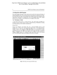
the dialog box pops up as shown in the Figure 5.1.
Figure 5.1 ICLink dialog box showing selection for creation of the GSDII intermediate form file.
11/28/07
EECS:4610 Digital Vlsi Design I
Project Support
Dr. Anthony D. Johnson
tlm_mos_07.fm - 9
5.23 Making selections in the IClink dialog box
In the IClink dialog box select:
Source Format: ICgraph,
Destination Format: GDSII,
OK
after which the ICgraph: From ICgraph to GDSII window pops up, as shown in Figure 5.2
ICgraph: From ICgraph to GDSII dialog box showing selection of ICLink
options fille.
Fig 5.2
5.24 Generating the.gds file
In the ICgraph: From ICgraph to GDSII window enter,
ICgraph cell: <project_name> (the name of the final design)
GDSII file: <project_name>.gds (the name with extension.gds)
Options file: $ADK/lib/iclink_gdsii.options
OK
after which the message appears at the bottom of the IC window,
"Starting conversion"
then after a longer time another message appears,
“ICLink completed with errors"
which could include both errors and warnings; warnings can be ignored, errors must be fixed.
11/28/07
EECS:4610 Digital Vlsi Design I
Project Support
Dr. Anthony D. Johnson
tlm_mos_07.fm - 10
APPENDIX: PROBLEMS WHICH CAN BE ENCOUNTERED DURING THE DESIGN PROCESS
Certain problems can be encountered in the design process due to the lack of details in the descriptions
of the design process. There are also certain problems in the process of padframe generation.
IC station tends to duplicate some ports, which leads to the reporting of unplaced objects by the IClink,
even though the ICverify shows no errors and the design has passed the LVS check. Removing these
unplaced objects, will create new errors in the CIF file generation reported. These unplaced items can
be listed by selecting from the IC Station menu bar
Report → Group → members → Unplaced
When this problem was reported to the Mentor customer support group, they said that "Usually this
IClink "unplaced objects" refers not to polygon-based layout data but to logical entities such as ports for
example. If the design is verified as being clean by Calibre or ICverify and you are getting these
messages in the IClink log file, the design is ok. The verify tools ignore any logical entities that may be
unplaced or missing. This could occur by running SDL and not placing the ports or unplacing one of the
ports for example. If the unplaced objects cannot be found in the layout, the IClink messages can be
ignored if the verification turned out to be OK." (Unplaced objects which can be found are there but they
are not connected?)
Mentor Graphic ADK tools simplify the designing process.
REFERENCES
[1] Smith, M. J. S., Application-Specific Integrated Circuits, Addison-Wesley, Reading, Mass., 2001
[2] Huber, J.P., and Rosneck, M.W., Successful Asic Design the First Time Through, Van Nostrand
Reinhold, New York, 1991.
[3] Schroeter, J., Surviving the ASIC experience, Prentice-Hall, Englewood Cliffs, N.J.,1992
[4] Mentor Graphics, Designing ASICs with the ADK Design Kit and Mentor Graphics Tools, 2001
[5] Mentor Graphics, Design Architect User’s Manual version 2.0,
[6] Mentor Graphics, Getting Started with Design Architect, 1999
[7] Mentor Graphics, Design Viewpoint Editor User’s and Reference Manual, 1998.
[8] Mentor Graphics, Schematic Generator User’s and Reference Manual, 1998.
[9] Mentor Graphics, IC Station User’s Manual, 1999.
[10] Mentor Graphics Web Site, www.mentorg.com
[11] Mentor Graphics Higher Education
germanium.ee.wustl.edu/HEP/adk.htm
Program
[12] Mentor Graphics, ICStation Data Conversion Manual.
11/28/07
Technical
Support
Site,
http://