1
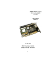
Sandpoint User’s Manual
Revision 1.01
Sandpoint
User’s Manual
6/9/99
Revision 1.01
Preliminary copy, subject to change without notice
Page 1 of 38
Revision 1.01
1
Sandpoint User’s Manual
OVERVIEW .................................................................................................................................................. 4
1.1
Revision History..................................................................................................................................... 4
1.2
Introduction............................................................................................................................................ 5
1.3
Purpose ................................................................................................................................................. 5
1.3
Reference Documents ........................................................................................................................... 6
1.3.1
Motorola Documents ....................................................................................................................... 6
1.3.2
External Documents........................................................................................................................ 6
2
PRODUCT SUMMARY ................................................................................................................................. 7
3
SYSTEM CONFIGURATION ........................................................................................................................ 8
3.1
4
5
Block Diagram ....................................................................................................................................... 8
CHASSIS...................................................................................................................................................... 9
4.1
Slots ...................................................................................................................................................... 9
4.3
External CONTROLS & INDICATORS................................................................................................. 10
4.4
External connectors ............................................................................................................................. 11
INSTALLATION .......................................................................................................................................... 12
5.1
Motherboard diagram........................................................................................................................... 12
5.2
Jumpers and connectors Description.................................................................................................... 13
5.2.1
J11, J12, J13 PPMC Connectors................................................................................................... 14
5.2.2
J13, J14, J21 and J22 32-bit and 64-bit PCI Slot ........................................................................... 17
5.2.3
J16, J17 COM Ports...................................................................................................................... 19
5.2.4
J18 Parallel Port ........................................................................................................................... 19
5.2.5
J19,J20 PS/2 Keyboard and Mouse Connector.............................................................................. 20
5.2.6
J23 ATX Power Connector ............................................................................................................ 21
5.2.7
J25 CMOS Battery Connector ....................................................................................................... 22
5.2.8
J26, J27 IDE Connectors............................................................................................................... 23
5.2.9
J28 Floppy Disk Connector ........................................................................................................... 24
5.2.10 J29 Misc. Connectors.................................................................................................................... 25
5.2.11 J33 Test Clock Input ..................................................................................................................... 26
5.2.12 J34 66MHZ PCI Disable................................................................................................................ 26
5.2.13 S1 Power ON/OFF Switch............................................................................................................ 27
5.2.14 S2 Reset Switch............................................................................................................................ 27
5.2.15 S3, S4 Mode Selection Switch ...................................................................................................... 28
5.2.16 S5 Interrupt Inversion Switch ........................................................................................................ 29
5.2.17 S6 Shared interrupt Selection Switch ............................................................................................ 30
5.2.18 J30, J31 and J32 VIO Selection .................................................................................................. 31
5.3
Boot ROM............................................................................................................................................ 32
Page 2 of 38
Sandpoint User’s Manual
6
Revision 1.01
5.4
RTC and NVRAM................................................................................................................................. 32
5.5
DISPLAY ............................................................................................................................................. 32
5.6
IDE DRIVE (s)...................................................................................................................................... 32
5.7
Hard Drive Activity Indicator ................................................................................................................ 32
5.8
Floppy Drive(s) .................................................................................................................................... 32
5.9
Speaker ............................................................................................................................................... 33
5.10
Power Supply....................................................................................................................................... 33
KEY COMPONENTS .................................................................................................................................. 34
6.1
Winbond 83C553 ................................................................................................................................. 34
6.2
National Semiconductor PC87308........................................................................................................ 34
7
DINK32 DEBUG MONITOR ........................................................................................................................ 35
8
INTERRUPT CONFIGURATION................................................................................................................. 36
9
PCI SLOT INFORMATION.......................................................................................................................... 37
APPENDIX A: INTERCONNECTION DIAGRAM................................................................................................ 38
Page 3 of 38
Revision 1.01
Sandpoint User’s Manual
1
OVERVIEW
1.1
REVISION HISTORY
Date
Revision
Distribution
Comments
2/21/99
6/9/99
1.0
1.01
General Release ....................................For Sandpoint 1.0
General Release ....................................Correction on jumper setting description
on S5 and S6.
Please email your comments of this user’s manual to:
RISC Hotline
Email: [email protected]
TRADEMARKS
The PowerPC name, the PowerPC logotype, PowerPC 603, PowerPC740, and PowerPC750 and are
trademarks of International Business Machines Corporation used by Motorola under license from
International Business Machines Corporation
All other trademarks are the property of their respective owner(s)
This document contains information on a new product under development. Specifications and
information
herein are subject to change without notice.
Page 4 of 38
Sandpoint User’s Manual
1.2
Revision 1.01
INTRODUCTION
This document describes the features of the “Sandpoint” Processor PCI Mezzanine Card (PPMC) host
board. This board contains one PMC/PPMC – compatible slot, four PCI slots and complement of
standard PC motherboard logic such as an ISA bridge, serial, parallel, keyboard/mouse, floppy and IDE
disk controllers. Sandpoint is intended for hardware and software development and evaluation purpose
only, and is not intended for operation in commercial environments.
1.3
PURPOSE
The Sandpoint PPMC host board design has various uses including, but not limited to:
-
System suitable to showcase the 8240 PMC, 7XX PMC and the other future PPMC solution
-
System for use by customers in benchmarking, compatibility testing, firmware development etc.
-
Software debug platform for embedded application.
-
Development platform for use by third-parties firmware/utility developers.
It should be noted that Sandpoint is not intended only for purposes such as that outlined above and is not
intended to be sold as a Motorola product.
Page 5 of 38
Revision 1.01
Sandpoint User’s Manual
1.3
REFERENCE DOCUMENTS
1.3.1
Motorola Documents
-
1.3.2
PowerPC Microprocessor Family: The Programming Environments manual
PowerPC 603e User’s manual
PowerPC 740 User’s manual
PowerPC 750 User’s manual
PowerPC 106 Chipset Implementation Definition
PowerPC 8240 User’s manual
Sandpoint Hardware Reference Manual
External Documents
-
Page 6 of 38
Peripheral Component Interconnect (PCI) Specification Rev 2.1
Draft Standard Physical and Environmental layers for PCI Mezzanine Cards: PMC
(IEEE P1386.1/Draft 2.0 04-Apr-1995)
Draft Standard Physical and Environmental Layers for Processor PCI Mezzanine Cards: PPMC
(XXXX P1386.X/Draft 0.1 15-Feb-1998)
Draft Standard for a Common Mezzanine Card Family: CMC
(IEEE P1386/Draft 2.0 04-Apr-1995)
ATX Specification version 1.0
Sandpoint User’s Manual
2
Revision 1.01
PRODUCT SUMMARY
The Sandpoint motherboard is a “host” board, which accepts a PMC or PPMC card as well as up to four
PCI slots. The host board has the following features:
PMC and PPMC support
-
One PMC slot with PPMC, 64-bit and 66MHz extensions
Switch-selectable operating modes
Four PCI slots: 2 5V/32-bit slots, 2 3.3V/64-bit slots
PCI slots support 33 or 66 MHz operation
Two standard 16650-compatible ESD-protected serial ports
IEEE 1284 parallel port
Floppy disk port
Two IDE ports
PS/2 Mouse and keyboard connectors
NVRAM and real-time clock (RTC)
Advanced Power Controller (“soft on/off)
LED monitors for critical functions
Automatic sense of PCI bus speed (33 or 66 MHz)
Flash EPROM for boot firmware
ATX chassis with ATX power supply
DINK32 Debug Monitor Software in ROM
Notes: The I/O subsystem is identical to that of “EC”version of the Yellowknife development
platform,
Current PowerPC evaluation system. When properly configured, software written for the
Yellowknife platform should operate identically when executed on a Sandpoint.
Page 7 of 38
Revision 1.01
3
SYSTEM CONFIGURATION
3.1
BLOCK DIAGRAM
Sandpoint User’s Manual
The following is the block diagram of the Sandpoint:
Page 8 of 38
Sandpoint User’s Manual
4
Revision 1.01
CHASSIS
The Sandpoint use the ATX format chassis which had external drive bays for additional upgrade.
4.1
SLOTS
The Sandpoint chassis supports a total of four PCI slots for add-in cards. Two of the PCI slots are 32-bit
and reminding two are 64-bit slots.
Page 9 of 38
Revision 1.01
4.3
Sandpoint User’s Manual
EXTERNAL CONTROLS & INDICATORS
The following diagram shows the front panel of the Sandpoint system:
On-Off
Switch
Power On indicator
Reset
Switch
Page 10 of 38
Sandpoint User’s Manual
4.4
Revision 1.01
EXTERNAL CONNECTORS
The following show the back panel on the ATX chassis:
ATX Power Supply
Serial Port 1
PS/2 Keyboard
PS/2 mouse
Parallel Port
Optional
Serial and
Parallel
Ports
Serial Port 2
64-bit PCI
64-bit PCI
PCI Slot X 4
32-bit PCI
32-bit PCI
Page 11 of 38
Revision 1.01
5
INSTALLATION
5.1
MOTHERBOARD DIAGRAM
Sandpoint User’s Manual
The following is the Sandpoint motherboard diagram:
Page 12 of 38
Sandpoint User’s Manual
5.2
Revision 1.01
JUMPERS AND CONNECTORS DESCRIPTION
1) J11
2) J12
3) J13
4) J14
5) J15
6) J16
7) J18
8) J19
9) J20
10) J21
11) J22
12) J23
13) J25
14) J26
15) J27
16) J28
17) J29
18) J30,31,32
19) J33
20) J34
21) S1
22) S2
23) S3,S4
24) S5
25) S6
PMC Connector 1 (64-pin)
PMC connector 2 (64-pin)
PMC connector 3 (64-pin)
64-bit PCI slot
64-bit PCI slot
COM1 port
Parallel Port
PS/2 Keyboard connector
PS/2 Mouse connector
32-bit PCI slot
32-bit PCI slot
ATX Connector
Battery connector
Primary IDE connector
Secondary IDE connector
Floppy Disk connector
Misc. connectors (Reset, PowerON, Speaker)
VIO selection jumpers
Test Clock Input
66MHz PCI Disable
Power On/Off Switch
Reset Switch
Mode Selection Switch
Interrupt Inversion Switch
Shared Interrupt Selection Switch
Page 13 of 38
Revision 1.01
5.2.1
Sandpoint User’s Manual
J11, J12, J13 PPMC Connectors
2
J12
1
2
Pn2
2
J11
1
J13
1
Pn1
Pn3
Note: 8240 PMC uses only J11 and J12 connectors
Pn1/J11 32 Bit PCI pin description
Pin #
1
3
5
7
9
11
13
15
17
19
21
23
25
27
29
31
33
35
37
39
41
43
45
47
49
51
53
55
57
59
61
63
Signal Name
TCK
Ground
INTB#
PRESENT#
INTD#
Ground
PCICLK
Ground
REQ#/XGNT[0]#
V(I/O)
AD[28]
AD[25]
Ground
AD[22]
AD[19]
V(I/O)
FRAME#
Ground
DEVSEL#
Ground
SDONE#
PAR
V(I/O)
AD[12]
AD[09]
Ground
AD[06]
AD[04]
V(I/O)
AD[02]
AD[00]
Ground
Page 14 of 38
Signal Name
-12V
INTA#
INTC#
+5V
PCI-RSVD
PCI-RSVD
Ground
GNT#/XREQ[0]#
+5V
AD[31]
AD[27]
Ground
C/BE[3]#
AD[21]
+5V
AD[17]
Ground
IRDY#
+5V
LOCK#
SBO#
Ground
AD[15]
AD[11]
+5V
C/BE[0]#
AD[05]
Ground
AD[03]
AD[01]
+5V
REQ64#
Pin #
2
4
6
8
10
12
14
16
18
20
22
24
26
28
30
32
34
36
38
40
42
44
46
48
50
52
54
56
58
60
62
64
Sandpoint User’s Manual
Revision 1.01
Pn2/J12 32Bit PCI Pin Description
Pin #
1
3
5
7
9
11
13
15
17
19
21
23
25
27
29
31
33
35
37
39
41
43
45
47
49
51
53
55
57
59
61
63
Signal Name
+12V
TMS
TDI
Ground
PCI-RSVD
XREQ[1]#
RST#
+3.3V
PCI-RSVD
AD[30]
Ground
AD[24]
IDSEL
+3.3V
AD[18]
AD[16]
Ground
TRDY#
Ground
PERR#
+3.3V
C/BE[1]#
AD[14]
M66EN
AD[08]
AD[07]
+3.3V
XGNT[1]#
XGNT[2]#
Ground
ACK64#
Ground
Signal Name
TRST#
TDO
Ground
PCI-RSVD
PCI-RSVD
+3.3V
XREQ[2]#
XREQ[3]#
Ground
AD[29]
AD[26]
+3.3V
AD[23]
AD[20]
Ground
C/BE[2]#
PMC-RSVD
+3.3V
STOP#
Ground
SERR#
Ground
AD[13]
AD[10]
+3.3V
PMC-RSVD
PMC-RSVD
Ground
XGNT[3]#
PMC-RSVD
+3.3V
SYSCON#
Pin #
2
4
6
8
10
12
14
16
18
20
22
24
26
28
30
32
34
36
38
40
42
44
46
48
50
52
54
56
58
60
62
64
Page 15 of 38
Revision 1.01
Sandpoint User’s Manual
Pn3/J13 64 Bit PCI Pin Description
Pin #
1
3
5
7
9
11
13
15
17
19
21
23
25
27
29
31
33
35
37
39
41
43
45
47
49
51
53
55
57
59
61
63
Signal Name
PCI-RSVD
Ground
C/BE[6]#
C/BE[4]#
V(I/O)
AD[63]
AD[61]
Ground
AD[59]
AD[57]
V(I/O)
AD[55]
AD[53]
Ground
AD[51]
AD[49]
Ground
AD[47]
AD[45]
V(I/O)
AD[43]
AD[41]
Ground
AD[39]
AD[37]
Ground
AD[35]
AD[33]
V(I/O)
PCI-RSVD
PCI-RSVD
Ground
Page 16 of 38
Signal Name
Ground
C/BE[7]#
C/BE[5]#
Ground
PAR64
AD[62]
Ground
AD[60]
AD[58]
Ground
AD[56]
AD[54]
Ground
AD[52]
AD[50]
Ground
AD[48]
AD[46]
Ground
AD[44]
AD[42]
Ground
AD[40]
AD[38]
Ground
AD[36]
AD[34]
Ground
AD[32]
PCI-RSVD
Ground
PCI-RSVD
Pin #
2
4
6
8
10
12
14
16
18
20
22
24
26
28
30
32
34
36
38
40
42
44
46
48
50
52
54
56
58
60
62
64
Sandpoint User’s Manual
5.2.2
Revision 1.01
J13, J14, J21 and J22 32-bit and 64-bit PCI Slot
Slot 3
J21-32-bit
Slot 4
J22-32-bit
Slot 1
Slot 2
J14-64-bit
J15-64-bit
Sandpoint has three PCI slots (PCI 1, PCI 2 and PCI 3). The connectors, pin assignments, signal timings,
loadings and mechanical dimensions all conform to the standard PCI specification. The pin assignment for the
PCI connectors is as follows:
Pin
B1
B2
B3
B4
B5
B6
B7
B8
B9
B10
B11
B12
B13
B14
B15
B16
B17
B18
B19
B20
B21
B22
B23
B24
B25
B26
B27
B28
B29
B30
B31
B32
B33
B34
B35
B36
B37
B38
B39
Description
-12V
TCK
GROUND
TD0
+5V
+5V
INTB*
INTD*
PRSNT1*
RESERVED
PRSNT2*
GROUND
GROUND
RESERVED
GROUND
CLK
GROUND
REQ*
+5V (I/O)
AD31
AD29
GROUND
AD27
AD25
+3.3V
C/BE*3
AD23
GROUND
AD21
AD19
+3.3V
AD17
C/BE*2
GROUND
IRDY*
+3.3V
DEVSEL*
GROUND
LOCK*
Pin
A1
A2
A3
A4
A5
A6
A7
A8
A9
A10
A11
A12
A13
A14
A15
A16
A17
A18
A19
A20
A21
A22
A23
A24
A25
A26
A27
A28
A29
A30
A31
A32
A33
A34
A35
A36
A37
A38
A39
Description
TRST*
+12V
TMS
TDI
+5V
INTA*
INTC*
+5V
RESERVED
+5V
RESERVED
GROUND
GROUND
RESERVED
RST*
+5V (I/O)
GNT*
GROUND
RESERVED
AD30
+3.3V
AD28
AD26
GROUND
AD24
IDSEL
+3.3V
AD22
AD20
GROUND
AD18
AD16
+3.3V
FRAME*
GROUND
TRDY*
GROUND
STOP*
+3.3V
Comment
32-bit connector starts
Page 17 of 38
Revision 1.01
Sandpoint User’s Manual
B40
PERR*
B41
B42
B43
B44
B45
B46
B47
B48
B49
B50
B51
B52
B53
B54
B55
B56
B57
B58
B59
B60
B61
B62
+3.3V
SERR*
+3.3V
C/BE*1
AD14
GROUND
AD12
AD10
GROUND
(KEY)
(KEY)
AD8
AD7
+3.3V
AD5
AD3
GROUND
AD1
+5V (I/O)
ACK64*
+5V
+5V
B63
B64
B65
B66
B67
B68
B69
B70
B71
B72
B73
B74
B75
B76
B77
B78
B79
B80
B81
B82
B83
B84
B85
B86
B87
B88
B89
B90
B91
B92
B93
B94
Page 18 of 38
RESERVED
GROUND
C/BE[6]#
C/BE[4]#
GROUND
AD[63]
AD[61]
+3.3V
AD[59]
AD[57]
GROUND
AD[55]
AD[53]
GROUND
AD[51]
AD[49]
+3.3V
AD[47]
AD[45]
GROUND
AD[43]
AD[41]
GROUND
AD[39]
AD[37]
+3.3V
AD[35]
AD[33]
GROUND
RESERVED
RESERVED
GROUND
A40
A41
A42
A43
A44
A45
A46
A47
A48
A49
A50
A51
A52
A53
A54
A55
A56
A57
A58
A59
A60
A61
A62
Connector Key
A63
A64
A65
A66
A67
A68
A69
A70
A71
A72
A73
A74
A75
A76
A77
A78
A79
A80
A81
A82
A83
A84
A85
A86
A87
A88
A89
A90
A91
A92
A93
A94
SDONE
32-bit connectors
continued
SBO*
GROUND
PAR
AD15
+3.3V
AD13
AD11
GROUND
AD9
(KEY)
(KEY)
C/BE*0
+3.3V
AD6
AD4
GROUND
AD2
AD0
+5V (I/O)
REQ64*
+5V
+5V
64-bit spacer
GROUND
C/BE[7]#
C/BE[5]#
+3.3V
PAR64
AD[62]
GROUND
AD[60]
AD[58]
GROUND
AD[56]
AD[54]
+3.3V
AD[52]
AD[50]
GROUND
AD[48]
AD[46]
GROUND
AD[44]
AD[42]
+3.3V
AD[40]
AD[38]
GROUND
AD[36]
AD[34]
GROUND
AD[32]
RESERVED
GROUND
RESERVED
64-bit connector start
64-bit connector end
Sandpoint User’s Manual
5.2.3
Revision 1.01
J16, J17 COM Ports
Sandpoint has two 16550-compatible serial ports. PC serial connectors are located
at the back panel.
PC serial port pin assignment
J17- COM2
1
J16- COM1
Pin
1
2
3
4
5
6
7
8
9
5.2.4
Signal
DCD
SIN
SOUT
DTR
GND
DSR
RTS
CTS
RI
I/O
I
I
O
O
N/A
I
O
I
I
5
6
9
Definition
Data carrier detect
Serial input
Serial output
Data terminal ready
Signal GND
Data Set Ready
Request To Send
Clear To Send
Ring Indicator
J18 Parallel Port
Sandpoint has one AT-compatible, bi-directional parallel port. This connector is located at the back
panel.
J18
1
1
2
1
Page 19 of 38
Revision 1.01
Sandpoint User’s Manual
Pin
1
2
3
4
5
6
7
8
9
10
11
12
13
14
15
16
17
18-25
5.2.5
Signal
STB#
PD0
PD1
PD2
PD3
PD4
PD5
PD6
PD7
ACK#
BUSY
PE
SLCT
AFD#
ERR#
INIT#
SLIN#
GND
I/O
I/O
I/O
I/O
I/O
I/O
I/O
I/O
I/O
I/O
I
I
I
I
O
I
O
O
N/A
Definition
Strobe
Printer data bit o
Printer data bit 1
Printer data bit 2
Printer data bit 3
Printer data bit 4
Printer data bit 5
Printer data bit 6
Printer data bit 7
Acknowledge
Busy
Paper end
Select
Automatic Feed
Error
Initialize printer
Select in
Signal GND
J19,J20 PS/2 Keyboard and Mouse Connector
Sandpoint supports both the AT-compatible keyboard interfaces. PS/2 keyboard connectors are
located at the back panel.
J19 PS/2 Keyboard
6
5
4
2
The following is the PS/2 Keyboard pin definition:
Pin
1
2
3
4
5
6
Page 20 of 38
Signal
KBDATA
NC
GND
FVcc
KBCLK
NC
3
I/O
I/O
N/A
N/A
N/A
I/O
N/A
Definition
Keyboard data
No connection
Signal GND
Fused supply voltage
Keyboard clock
No connection
1
Sandpoint User’s Manual
Shell
N/A
N/A
Revision 1.01
Chassis GND
Sandpoint supports both the PS/2 compatible mouse The PS/2 mouse is supported through the
mouse port. PS/2 mouse connector is located at the back panel.
PS/2 mouse connector pin assignment
J19 PS/2 Mouse
6
5
4
3
2
Pin
1
2
3
4
5
6
Shell
5.2.6
Signal
MFDATA
NC
GND
FVcc
I/O
I/O
N/A
N/A
N/A
KBCLK
NC
N/A
I/O
N/A
N/A
1
Definition
Mouse data
No connection
Signal GND
Fused supply
voltage
Mouse clock
No connection
Chassis GND
J23 ATX Power Connector
Sandpoint uses the standard ATX power supply, which provide the 5V and 3.3V to the motherboard. The
following is the power connector pin assignment:
1
Page 21 of 38
Revision 1.01
Sandpoint User’s Manual
Pin
1
2
3
4
5
6
7
8
9
10
5.2.7
Signal
+3.3V
+3.3V
GND
VCC
GND
VCC
GND
PWRGOOD
VSTDBY
+12V
Pin
11
12
13
14
15
16
17
18
19
20
Signal
+3.3V
-12V
GND
PS_ON
GND
GND
GND
-5V
VCC
VCC
J25 CMOS Battery Connector
1
Connect the CMOS battery connector to either 1-4
Page 22 of 38
Battery
Key
NC
GND
Sandpoint User’s Manual
5.2.8
Revision 1.01
J26, J27 IDE Connectors
The Enhanced IDE controller is built in the PCI-ISA bridge, two IDE connectors are on the motherboard
to support both the enhanced IDE hard drives and the IDE CD-ROM. The IDE controller is part of the
Winbond 553. See the Winbond 553 data book for additional information on the IDE controller.
J26
1
J27
1
IDE1
IDE2
IDE connector pin assignment
Pin
1
3
5
7
9
11
13
15
17
19
21
23
25
27
29
31
33
35
37
39
Signal
IDERESET#
IDED7
IDED6
IDED5
IDED4
IDED3
IDED2
IDED1
IDED0
GROUND
IDEDRQ#
IDEIOW#
IDEIOR#
N/C
IDEACK#
IDEIRQ
IDESA1
IDESA0
IDECS0#
DISKLED#
Pin
2
4
6
8
10
12
14
16
18
20
22
24
26
28
30
32
34
36
38
40
Signal
GND
IDED8
IDED9
IDED10
IDED11
IDED12
IDED13
IDED14
IDED15
N.C.
GND
GND
GND
IDEBALE
GND
IDEIOCS16#
N.C.
IDESA2
IDECS1#
GND
Page 23 of 38
Revision 1.01
5.2.9
Sandpoint User’s Manual
J28 Floppy Disk Connector
Sandpoint incorporates a 34-pin Floppy disk connector to support the floppy disk drive. The floppy
controller is in the National 308 Super I/O chip. See National 308 data book for additional information.
J28
1
The pin assignment of the PC standard floppy disk drive is as follows:
Pin
1
3
5
7
9
11
13
15
17
19
21
23
25
27
29
31
33
Page 24 of 38
Signal
Gnd
Gnd
Gnd
NC
Gnd
Gnd
Gnd
Gnd
MSEN1
Gnd
Gnd
Gnd
Gnd
MSEN0
Gnd
Gnd
Gnd
Pin
2
4
6
8
10
12
14
16
18
20
22
24
26
28
30
32
34
Signal
DENSEL
NC
NC
INDEX#
MTR0#
DRVSEL1#
DRVSEL0#
MTR1#
DIR#
STEP#
WDATA#
WGATE#
TRK0#
WRTPRT#
RDATA#
HDSEL#
DSKCHG#
Sandpoint User’s Manual
Revision 1.01
5.2.10 J29 Misc. Connectors
J29
SPKR
PWR LED
IR Port
1
2
PWR
Switch
Pin
1
3
5
7
9
11
13
15
17
19
21
23
25
27
29
31
33
STDBY PS on
LED
Signal
VCC
NC
IRRX
GND
IRTX
NC
VCC
NC
GND
NC
GND
NC
NC
PCSPKR
NC
GND
VCC
Pin
2
4
6
8
10
12
14
16
18
20
22
24
26
28
30
32
34
Disk LED
Reset
Signal
GND
RSTHDR#
GND
NC
NC
VCC
DISKLED#
DISKLED#
VCC
PS_ON#
GND
NC
VSTDBY
GND
NC
PWR_A
PWR_B
Page 25 of 38
Revision 1.01
Sandpoint User’s Manual
5.2.11 J33 Test Clock Input
J33
If jumper J33 is installed, the on-board 66MHz oscillator is disabled and an external clock source is used
to drive the PCI bus. The signal provided must be 3.3V LVTTL logic levels into a 50 ohms Load. The
input clock is supplied as-is, or divided by two, depending upon the state of the M66EN (66MHz PCI)
status and the 66MHz PCI Disable jumper.
Care must be used that the devices receiving the clock are capable of and are configured to operate at
the new clock speed. In particular, PowerPC devices have internal PLLs, which require a minimum clock
input to operate properly.
5.2.12 J34 66MHZ PCI Disable
J34
If jumper 34 is installed, the PCI bus will operate at 33MHz regardless of the status of the M66EN signal.
The PCI bus ordinarily selects 66 MHz operation if (and only if) all PPMC and PCI devices installed
support 66 MHz clock rates; otherwise, the slower 33MHz rate is used. However, for testing purposes,
this jumper may be used to evaluate slower bus clock rates. In addition, it may be needed for systems
using 66MHz-capable cards which also wish to use the Winbond or on-board I/O. Since these devices
operate at 33MHz only, yet do not have an M66EN pin to control clock selection, jumper J34 is required
to force the PCI bus to operate at 33MHz.
Page 26 of 38
Sandpoint User’s Manual
Revision 1.01
5.2.13 S1 Power ON/OFF Switch
S1
Press once to power up the system. Press again to power off the system.
SEE ERRATA
5.2.14 S2 Reset Switch
S2
Press once to reset the system
Page 27 of 38
Revision 1.01
Sandpoint User’s Manual
5.2.15 S3, S4 Mode Selection Switch
Mode 0: PMC W/IDE
Mode 2: PMC/Winbond
Mode 1: PMC W/Slots
Mode 3: Yellowknife
To support existing Yellowknife/PPMC software environment, as well as the new Sandpoint/PPMC
environment, Sandpoint supports four different modes, which are selectable via a pair of switches. The
following table describes the modes.
Mode
Default 0
Name
PPMC
With IDE
Host
1
PPMC Host with
Slots
2
PPMC/Winbond
3
Yellowknife
Description
PPMC Host Mode W/IDE support: The PPMC slot is
the system controller and provides arbitration and
interrupt control. The Winbond IDE disk controllers
replace slots 1 and 2 (3.3V PCI slots). The 5V PCI slots
3 and 4 are available. The on-board I/O shares interrupts
with slots 2 or 3
PPMC Host Mode W/Four slot support: The PPMC
slot is the system controller and provides arbitration and
interrupt control. The Winbond IDE disk controllers are
unavailable. All slots are available. The on-board I/O
shares interrupts with slots 2 or 3
PPMC/Winbond Mode: The PMC slot is an agent, and
the Winbond provides arbitration and interrupt control.
The Winbond interrupt output drives the INTA# pin of the
PPMC slot.
Yellowknife Mode: The PPMC slot is an agent, and the
Winbond provides arbitration and interrupt control. The
Winbond interrupt output drives the INTA# pin of the
forth PCI slot.
Which mode should be selected? The first two modes are the principal modes, which will be used for
new development, and can be selected between by deciding whether four PCI slots are needed or IDE is
needed.
Page 28 of 38
Sandpoint User’s Manual
Revision 1.01
The Latter two modes are intended as transitional settings, and may be used to aid conversion from a
modified Yellowknife platform, where a PPMC is connected through a PMC->PCI adapter card. This
Yellowknife system is identical to a Sandpoint operating in mode 3. Mode 2 is architecturally similar
except that the adapter card may be eliminated. Mode 2 is also useful for early PPMC cards such as the
PPMC750, which do not include a PCI arbiter, since the Winbond provides this feature.
The Sandpoint board uses switches to select one of the four configuration choices. Logic on the
Sandpoint host board switches the connections of the PCI request/grant signals, the PCI interrupt
signals, and the component configuration mode (SYSCON#, ARBDIS#, etc) to provide the required
environment. Appendix A shows how the different signals on the motherboard are interconnected.
5.2.16 S5 Interrupt Inversion Switch
Interrupt to PMC inverted
S5
S5
Interrupt to PMC normal
Some PPMC cards, such as the PPMC8240, are configured with active-high interrupt input when
operated in the default configuration, which conflicts with PCI requirements. This is one example in
which the MPC8240 is not quite identical to an MPC603+MPC106, so software moved as-is from the
Yellowknife to the PPMC8240 will find interrupts are not working. The short term work-around is to
configure Sandpoint to invert the PMC interrupt signal; since this violates the specs, it is intended only
for a short term assistance; the correct solution is to program the EPIC of the MPC8240 to accept the
correct polarity.
Page 29 of 38
Revision 1.01
Sandpoint User’s Manual
5.2.17 S6 Shared interrupt Selection Switch
Local I/O shared with Slot 3
S6
S6
Local I/O shared with Slot 2
PPMC cards support up to four interrupt sources. When operating in modes 0 or 1, there are a total of
five possible interrupt sources (four slots and the winbond PIC (handling the local I/O resources such as
serial ports)). When on-board I/O is needed, it must be shared with or replace PCI devices in slot 2 or
slot 3. Software must poll multiple sources to determine the interrupt source if both the slot and local I/O
are needed; otherwise, the slot can be left unused or used with non-interrupting devices such as graphics
cards.
To select which slot replaces/shares interrupts with the Sandpoint local I/O, set the switch as shown
above. This switch setting is ignored when the board is configured in modes 2 or 3.
Page 30 of 38
Sandpoint User’s Manual
Revision 1.01
5.2.18 J30, J31 and J32 VIO Selection
Jumpers J30, J31 and J32 are used to set the I/O voltage signaling level for the PPMC card. As with PCI
slots, the PPMC slot provides the ability to provide I/O power on certain pins, and compatibility is
maintained using keying methods (for PCI slots, a key is present in the slot, while for PPMC slots, a
keying pin protrudes from the motherboard into the PPMC card). For flexibility in testing purposes,
Sandpoint allows any types of VIO-Keyed board to be installed, with the proper VIO selected by jumper
J30-J32.
NOTE: This flexibility requires that the Sandpoint be configured to match the PPMC card before
powering up.
NOTE: All three jumpers must be set in an identical fashion; if any are different,
the power supply will short and the board can be damaged or destroyed.
5V VIO
3.3V VIO
5V
J30
5V
J30
VIO
J32
VIO
J32
3.3V
J31
3.3V
J31
Page 31 of 38
Revision 1.01
5.3
Sandpoint User’s Manual
BOOT ROM
ROM
Sandpoint incorporates a boot ROM which is implemented as a 4Mb (512Kbx8) flash EPROM.
The BootROM contains the DINK32 boot code to support basic debug
function. See the DINK32 user’s manual for more information.
The boot ROM is physically located on the ISA bus.
5.4
RTC AND NVRAM
Sandpoint incorporates an 8 KB battery-backed SRAM, which is organized as 8Kbx8 and is used for the
storage of system configuration information such as:
-
5.5
Passwords
Boot record
Global environment parameters
Language data
DISPLAY
Sandpoint communicate with the terminal through serial port 1, the terminal needs to be VT-100
compatible.
5.6
IDE DRIVE (S)
Sandpoint includes logic for a PCI bus Master IDE Interface. Two connectors are located on the
motherboard to support the primary and secondary interface.
5.7
HARD DRIVE ACTIVITY INDICATOR
The Sandpoint chassis incorporates a hard disk drive activity indicator that is ON when data is being
transferred to/from any internal IDE drive.
5.8
FLOPPY DRIVE(S)
Sandpoint supports 3.5” standard PC floppy disk drive.
Page 32 of 38
Sandpoint User’s Manual
5.9
Revision 1.01
SPEAKER
A PC-type 2.5”--diameter speaker is mounted on the inside of the chassis.
5.10
POWER SUPPLY
Sandpoint incorporates a ATX format 250W PC-type power supply capable of supplying sufficient power
at all required voltages to meet the needs of the supported motherboard, drives and add-in cards.
The power supply is switchable externally between 100V/60Hz and 220V/50Hz operations.
Page 33 of 38
Revision 1.01
6
Sandpoint User’s Manual
KEY COMPONENTS
The following table summarizes the key components used in the Sandpoint system:
PCI-ISA Bridge
I/O Controller
Enhanced IDE controller
NVRAM (RTC)
6.1
Winbond 83C553
National Semi PC87308VUL
Built in the Winbond 83C553
Built in PC87308VUL
WINBOND 83C553
The Sandpoint system uses the Winbond 83C553 PCI-ISA controller as a bridge to the ISA bus. This
bridge provides the following functions:
- 100% PCI and ISA compatible
- Incorporates two 8237 DMA controllers
- High performance PCI arbiter
- Incorporates two 8259 interrupt controllers
- One 82C54 16-bit counter/timer
- Bus master IDE support for 4 IDE devices
For more information on the Winbond chip, please refer to their user’s manual.
6.2
NATIONAL SEMICONDUCTOR PC87308
The PC87308 is a single chip super I/O controller. It incorporates in one fully Plug and Play compatible
chip, a Floppy Disk controller, a Keyboard and mouse controller, a Real-time clock. two full function
UARTs, infrared support, a full IEEE 1284 parallel port, three general purpose chip select signals, and
support for power management functions.
PC87308 also provide interface to the external SRAMs to provide the NVRAM functions.
Page 34 of 38
Sandpoint User’s Manual
7
Revision 1.01
DINK32 DEBUG MONITOR
.
Sandpoint is shipped with DINK32 boot firmware. DINK32 is a flexible software tool enabling evaluation
and debugging of the PowerPC 32-bit microprocessor. DINK32 is designed to be both a hardware and
software-debugging tool. DINK32 was written in ANSI C and built with modular routines around a central
core. Only a few necessary functions were written in PowerPC assembly.
The DINK32 provides the following functions:
•
•
•
•
•
•
•
•
•
•
Modification and display of general purpose, floating point, and special purpose registers
Assembly and disassembly of PowerPC instructions for modification and display of code
Single-step race and continued execution from a specified address
Modification, display, and movement of system memory
Setting, displaying and removing breakpoints
Automatic decompression of compressed s-record files while downloading
Extensive on-line help
Ability to execute user-assembled and/or download software in a controlled environment
Logging function for generating a transcript of a debugging session
Two command sets for novice and experienced users
Please refer
information.
to
http://www.mot.com/SPS/PowerPC/teksupport/tools/DINK32/index.html
for
more
Page 35 of 38
Revision 1.01
8
Sandpoint User’s Manual
INTERRUPT CONFIGURATION
The following table descirbes the interrupt sources seen by the PMC when the Sandpoint has been
configured for mode 0. This is the default configuration, and assumes that the on-board I/O interrupt is
shared with slot 1 (also the default)
0
Slot 1
INTA#
Slot 2
INTB#
Slot 3
INTC#
Slot 4
INTD#
PMC Interrupt Line (INT(0-3))
1
2
Slot 2
Slot3
INTA#
INTA#
Slot 3
Slot 4
INTB#
INTB#
Slot 4
Slot 1
INTC#
INTC#
Slot 1
Slot 2
INTD#
INTD#
SIOINT#
Page 36 of 38
Description
3
Slot 4
INTA#
Slot 1
INTB#
Slot 2
INTC#
Slot 3
INTD#
Each slot’s primary interrupt output (INTA) is routed to a
corresponding interrupt input on the PMC card.
On-board I/O interrupts are shared with “slot 2” by
default
Sandpoint User’s Manual
9
Revision 1.01
PCI SLOT INFORMATION
The following table describes the PCI slot information of the Sandpoint host board. This information is
constant for any mode selected.
PCI Slot/
Device
Physical Location
Configuratio
n
IDSEL
Configuratio
n
Address
Winbond
1
2
N/A
Second-nearest PMC
Nearest PMC
AD11
AD13
AD14
0x8000_08XX
0x8000_20XX
0x8000_40XX
3
4
Third-from PMC
Furthest from PMC
AD15
AD16
0x8000_80XX
0x8001_00XX
Note
Slot 1 and 2 are mis-labeled on
Sandpoint X2 version; the actual
ordering is 2-1-4-3 (from the PMC
outward)
Slot 3
Slot 4
Slot 1
Slot 2
For Sandpoint
X2
Only
Page 37 of 38
Revision 1.01
Sandpoint User’s Manual
APPENDIX A: INTERCONNECTION DIAGRAM
Page 38 of 38


![UK User`s Manual [ Notebook ]](http://vs1.manualzilla.com/store/data/005694610_1-ad8e24898a53e900e9c2a73fa8f500a7-150x150.png)