1
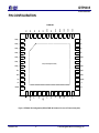
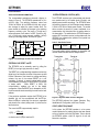
IDTP9035
Product Datasheet
THEORY OF OPERATION
The IDTP9035 is a highly-integrated WPC1 (Wireless
Power Consortium)-compliant wireless power charging IC
solution for the transmitter base station. It can deliver
more than 5W of power to the receiver when used with the
IDTP9020 or 5W in WPC “Qi” mode using near-field
magnetic induction as a means to transfer energy. It is the
industry’s first 5V single-chip WPC-compliant solution
designed to drive a WPC-compliant Type-A5/A11
transmitter coil.
OVERVIEW
Figure 2 shows the block diagram of the IDTP9035.
When 5V is applied at the 5V_A-G pins with EN
¯¯ at a logic
LOW, the Enable Sequence circuitry activates the voltage
reference, the 2.5V LDO, and the Driver Control for the
output inverter.
The voltage at the output of the LDO is monitored to
ensure that it remains in regulation, and the adaptor
voltage, coil current, and internal temperature are
monitored for proper operation.
The Driver Control block converts a PWM signal
(generated by the digital block and MCU) to the gate drive
signals required by the output inverter to drive the external
field-generating coil.
Communication packets from the receiver in the mobile
device are recovered by the Demodulator and converted
to digital signals that can be read by the MCU.
Several internal voltages are converted to their digital
representations by the ADC and supplied to the MCU.
Three GPIO ports are available to the system designer for
driving LEDs and a buzzer. The clock for the MCU and
other circuitry is generated an internal RC oscillator. I2C
SDA and SCL pins permit communication with an external
device or host.
OVER-CURRENT/TEMPERATURE PROTECTION
The current in the inverter is monitored by an analog
Current Limit block. If the instantaneous coil current
exceeds the OCP level, the upper switch in the inverter
will be turned off and the lower switch will be turned on for
the remainder of the cycle. The internal temperature is
also monitored, and the part is temporarily deactivated if
the temperature exceeds 140°C and reactivated when the
temperature falls below 110°C.
DRIVER CONTROL BLOCK and INVERTER
The Driver Control block contains the logic, shoot-through
protection, and gate drivers for the on-chip power FETs
and external FETs. The on-chip and external FETs are
configured as a full-bridge power inverter, effectively
doubling the peak-to-peak voltage applied to the coil. The
frequency of the full-bridge output waveform is set by the
MCU. (For details, please refer to the simplified
application diagram (Figure 1) and the reference design
schematic (Figure 9)).
DEMODULATOR
Power is transferred from the transmitter to the receiver
through the coupling of their respective coils: a looselycoupled transformer. The amount of power transferred is
determined by the transmitter’s switching frequency
(110kHz-205kHz, by WPC1), and is controlled by the
receiver through instructions it sends back through the
coils to the transmitter to change its frequency, end power
transfer, or do something else. The instructions take the
form of data packets, which are coupled through a series
of filters connected to the IDTP9035’s Demodulator
through the HPF pin. Recovering the data packets is the
function of the Demodulator. Decoding and executing the
packets is one of the functions of the MCU.
MICRO-CONTROLLER UNIT (MCU)
Note
1
Refer
to
the
WPC
specification
http://www.wirelesspowerconsortium.com/ for the most current information
Revision 1.0.2
15
at
The IDTP9035’s MCU processes the algorithm,
commands, and data that control the power transferred to
the reciever. The MCU is provided with RAM and ROM,
and parametric trim and operational modes are set at the
factory through the One-Time Programming (OTP) block,
read by the MCU at power-up.
© 2012 Integrated Device Technology, Inc.