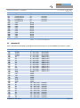
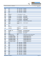
1
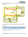
eCM-BF561 Hardware User Manual Version 1.4 Contact Bluetechnix Mechatronische Systeme GmbH Waidhausenstraße 3/19 A-1140 Vienna AUSTRIA [email protected] http://www.bluetechnix.com Date: 2013-06-18 Template No.: 900-306 / A Table of Contents 1 2 3 Introduction ...................................................................................................................................... 5 1.1 Overview ................................................................................................................................... 5 1.2 Applications............................................................................................................................... 6 General Description .......................................................................................................................... 7 2.1 Functional Description .............................................................................................................. 7 2.2 Boot Mode ................................................................................................................................ 7 2.3 Memory Map ............................................................................................................................. 7 2.3.1 Core Module Memory ........................................................................................................ 7 2.3.2 Externally Addressable Memory (on connector)................................................................ 8 Specifications ................................................................................................................................... 9 3.1 4 5 6 7 Electrical Specifications ............................................................................................................ 9 3.1.1 Operating Conditions ......................................................................................................... 9 3.1.2 Maximum Ratings .............................................................................................................. 9 3.1.3 ESD Sensitivity ................................................................................................................... 9 Connector Description ................................................................................................................... 10 4.1 Connector X1 .......................................................................................................................... 10 4.2 Connector X2 .......................................................................................................................... 12 Application Information .................................................................................................................. 15 5.1 Supply Voltage Decoupling ..................................................................................................... 15 5.2 Reset circuit ............................................................................................................................ 15 5.3 Application Example Schematics ........................................................................................... 15 Mechanical Outline ......................................................................................................................... 16 6.1 Top View ................................................................................................................................. 16 6.2 Bottom View ............................................................................................................................ 16 6.3 Side View................................................................................................................................. 17 6.4 Footprint .................................................................................................................................. 18 6.5 Connectors .............................................................................................................................. 18 Support ........................................................................................................................................... 19 7.1 General Support ...................................................................................................................... 19 7.2 Board Support Packages ........................................................................................................ 19 7.3 Blackfin® Software Support ................................................................................................... 19 7.3.1 BLACKSheep® OS .......................................................................................................... 19 7.3.2 LabVIEW .......................................................................................................................... 19 7.3.3 uClinux ............................................................................................................................. 19 7.4 Blackfin® Design Services ....................................................................................................... 19 7.4.1 Upcoming Products and Software Releases .................................................................. 19 Template No.: 900-306 / A 8 Ordering Information ...................................................................................................................... 20 8.1 9 Predefined mounting options for CORE MODULE NICKNAME ............................................. 20 Dependability ................................................................................................................................. 21 9.1 10 MTBF ....................................................................................................................................... 21 Product History ........................................................................................................................... 22 10.1 Version Information ............................................................................................................. 22 10.1.1 eCM-BF561-C-C-Q25S128F32 (eCM-BF561) ................................................................ 22 10.1.2 eCM-BF561-C-I-Q25S128F32 ........................................................................................ 22 10.2 Anomalies ............................................................................................................................ 22 11 Document Revision History ........................................................................................................ 23 12 List of Abbreviations ................................................................................................................... 24 A List of Figures and Tables .............................................................................................................. 25 Template No.: 900-306 / A © Bluetechnix GmbH 2013 All Rights Reserved. The information herein is given to describe certain components and shall not be considered as a guarantee of characteristics. Terms of delivery and rights of technical change reserved. We hereby disclaim any warranties, including but not limited to warranties of non-infringement, regarding circuits, descriptions and charts stated herein. Bluetechnix makes and you receive no warranties or conditions, express, implied, statutory or in any communication with you. Bluetechnix specifically disclaims any implied warranty of merchantability or fitness for a particular purpose. Bluetechnix takes no liability for any damages and errors causing of the usage of this board. The user of this board is responsible by himself for the functionality of his application. He is allowed to use the board only if he has the qualification. More information is found in the General Terms and Conditions (AGB). Information For further information on technology, delivery terms and conditions and prices please contact Bluetechnix (http://www.bluetechnix.com). Warning Due to technical requirements components may contain dangerous substances. Template No.: 900-306 / A Hardware User Manual - eCM-BF561 1 Last change: 18 June 2013 Version 1.4 Introduction The Core Module eCM-BF561 is optimized for performance and parallel data processing. The module integrates processor, RAM, flash and power supply at a size of 44x33mm! It is based on the high performance ADSP-BF561 from Analog Devices. The eCM-BF561 is designed for industrial and commercial applications. It addresses 128MByte SDRAM via its 32bit wide SDRAM bus and has an onboard NOR-flash of 32MByte. 1.1 Overview Figure 1-1 shows the main components of Core Module eCM-BF561. 100 Pin Expansion Connector PPI’s SPI UART JTAG SPORT’s ADSP-BF561 Low Voltage Reset 128MByte SDRAM 32MByte NOR Flash 100 Pin Expansion Connector eCM-BF561 Data/Address Bus GPIO’s POWER Ctrl Figure 1-1: Main components of the eCM-BF561 module • Analog Devices Blackfin Processor BF561 o Industrial version (see chapter Error! Reference source not found.) ADSP-BF561SBBCZ-5A (Rev 0.5;-40° - 85°C) o • Commercial version (see chapter Error! Reference source not found.) ADSP-BF561SKBCZ-6A (Rev 0.5; 0° - 70°C) U 128 MB SDRAM o Industrial version (see chapter Error! Reference source not found.) IS42S16320B-7BL SDRAM Clock up to 133MHz 2x (32Mx16, 512Mbit at 3.3V) o Commercial version (see chapter Error! Reference source not found.) IS42S16320B-7BL SDRAM Clock up to 133MHz 2x (32Mx16, 512Mbit at 3.3V) • 32 MB of Flash o PF48F4000P0ZBQE (16Mx16, 128Mbit at 3.3V; all 32MByte addressable) o Additional flash memory can be connected through the expansion board as parallel Flash using asynchronous chip select lines or as a SPI flash. • Core Voltage Regulator Template No.: 900-306 / A Page | 5 Hardware User Manual - eCM-BF561 o 1.35V • Low Voltage Reset Circuit o Module resets if power supply goes below 2.93V for at least 140ms • Connectors o SPORT 0 o SPORT 1 o UART o SPI o PPI-0 (Parallel Port Interface 0) o PPI-1 (Parallel Port Interface 1) o GPIO’s o Data Bus o Address Bus, Control Signals o nRESET o Boot-Mode o JTAG o Power Supply 1.2 Last change: 18 June 2013 Version 1.4 Applications • Parallel digital signal processing • Imaging and consumer multimedia • Set top boxes • Automotive vision systems • Portable media players • Digital video camera systems • Video conference applications Template No.: 900-306 / A Page | 6 Hardware User Manual - eCM-BF561 2 Last change: 18 June 2013 Version 1.4 General Description 2.1 Functional Description Figure 2-1: Functional Overview 2.2 Boot Mode By default the Boot Mode is set to 00 (BMODE0 pin = LOW, BMODE1 pin = LOW). The boot mode pins are available on the connectors. BMODE1–0 00 01 10 11 Description Execute from 16-bit external memory (Bypass Boot ROM) (uBoot, uClinux) 01 Boot from 8-bit/16-bit flash (BLACKSheep® OS) Boot from SPI host slave mode Boot from SPI serial EEPROM (16-, 24-bit address range) Table 2-1 Boot Mode 2.3 2.3.1 Memory Map Core Module Memory Memory Type FLASH *) SDRAM Start Address 0x20000000 0x00000000 End Address 0x21FFFFFF 0x07FFFFFF Size 32MB 128MB Comment Intel PF48F4000P0ZBQE 32Bit Bus, 2x ISSI IS42S16320-7BL Table 2-2: Memory Map *) Please be aware that you have to unlock the flash before starting an erase process! Template No.: 900-306 / A Page | 7 Hardware User Manual - eCM-BF561 2.3.2 Last change: 18 June 2013 Version 1.4 Externally Addressable Memory (on connector) The Blackfins External Bus Interface (EBI) allows connecting devices via an asynchronous memory interface. AMS Line nAMS1 nAMS2 nAMS3 Start Address 0x24000000 0x28000000 0x2C000000 End Address 0x27FFFFFF 0x2BFFFFFF 0x2FFFFFFF Max. Size 128MB 128MB 128MB Table 2-3: External Addressable Memory Template No.: 900-306 / A Page | 8 Hardware User Manual - eCM-BF561 3 Last change: 18 June 2013 Version 1.4 Specifications 3.1 3.1.1 Electrical Specifications Operating Conditions Symbol VIN I3V3 @ 25°C VOH VOL IIH IOZ fCCLK Parameter Input supply voltage 3.3V current High level output voltage Low level output voltage IO input current Three state leakage current Core clock frequency Min 3.0 2.4 100 Typical 3.3 700 - Max 3.6 0.4 10 10 600 Unit V mA V V µA µA MHz Table 3-1: Electrical characteristics 3.1.2 Maximum Ratings Stressing the device above the rating listed in the absolute maximum ratings table may cause permanent damage to the device. These are stress ratings only. Operation of the device at these or any other conditions greater than those indicated in the operating sections of this specification is not implied. Exposure to absolute maximum rating conditions for extended periods may affect device reliability. Symbol VIN VIO IOH /IOL TAMB TSTO φAMB Parameter Input supply voltage Input or output voltage Current per pin Ambient temperature Storage temperature Relative ambient humidity Min -0.3 -0.5 0 -40 -55 - Max 4.1 3.6 10 85 150 90 Unit V V mA °C °C % Table 3-2: Absolute Maximum Ratings 3.1.3 ESD Sensitivity ESD (electrostatic discharge) sensitive device. Charged devices and circuit boards can discharge without detection. Although this product features patented or proprietary protection circuitry, damage may occur on devices subjected to high energy ESD. Therefore, proper ESD precautions should be taken to avoid performance degradation or loss of functionality. Template No.: 900-306 / A Page | 9 Hardware User Manual - eCM-BF561 4 4.1 Last change: 18 June 2013 Version 1.4 Connector Description Connector X1 Please mind the mounted pull up, pull down and serial resistors on the Core Module (see column “Type”). Pin No. 1 2 3 4 5 6 7 8 9 10 11 12 13 14 15 16 17 18 19 20 21 22 23 24 25 26 27 28 29 30 31 32 33 34 35 36 37 38 39 40 41 42 43 44 Signal Name PPI0D0 PPI0D1 PPI0D2 PPI0D3 PPI0D4 PPI0D5 PPI0D6 PPI0D7 PPI0SYNC3 PPI0SYNC2/TMR9 PPI0SYNC1/TMR8 PPI0CLK GND PPI1D0 PPI1D1 PPI1D2 PPI1D3 PPI1D4 PPI1D5 PPI1D6 PPI1D7 PPI1D8/PF32 PPI1D9/PF33 PPI1D10/PF34 PPI1D11/PF35 PPI1D12/PF36 PPI1D13/PF37 PPI1D14/PF38 PPI1D15/PF39 PPI1SYNC3 PPI1SYNC2/TMR11 PPI1SYNC1/TMR10 PPI1CLK 3V3 3V3 3V3 GND GND GND NMI0 NMI1 RX/PF27 TX/PF26 GND Template No.: 900-306 / A Type I/O I/O I/O I/O I/O I/O I/O I/O I/O I/O I/O I Power I/O I/O I/O I/O I/O I/O I/O I/O I/O I/O I/O I/O I/O I/O I/O I/O I/O I/O I/O I Power Power Power Power Power Power I – 10k pull down I – 10k pull down I/O I/O Power Function PPI Data PPI Data PPI Data PPI Data PPI Data PPI Data PPI Data PPI Data PPI Sync PPI Sync PPI Sync PPI Clock PPI Data PPI Data PPI Data PPI Data PPI Data PPI Data PPI Data PPI Data PPI Data PPI Data PPI Data PPI Data PPI Data PPI Data PPI Data PPI Data PPI Sync PPI Sync PPI Sync PPI Clock Nonmaskable Interrupt Core A Nonmaskable Interrupt Core A UART Receive/GPIO UART Transmit/GPIO Page | 10 Hardware User Manual - eCM-BF561 Pin No. 45 46 47 48 49 50 51 52 53 54 55 56 57 58 59 60 61 62 63 64 65 66 67 68 69 70 71 72 73 74 75 76 77 78 79 80 81 82 83 84 85 86 87 88 89 90 91 92 93 94 95 Signal Name TCK TDO TDI TMS NTRST NEMU PF10 PF11 PF12 PF13 PF14 DT0SEC/PF17 DT0PRI/PF18 TFS0/PF16 TSCLK0/PF29 DR0SEC/PF20 DR0PRI RFS0/PF19 RSCLK0/PF28 GND CLKBUF GND SCK MISO MOSI nc nc DT1SEC/PF22 DT1PRI/PF23 TFS1/PF21 TSCLK1/PF31 DR1SEC/PF25 DR1PRI RFS1/PF24 RSCLK1/PF30 GND PF8 PF9 nc nc nc nc nc nc nc nc nc nc PPI0D15/PF47 PPI0D14/PF46 PPI0D13/PF45 Template No.: 900-306 / A Last change: 18 June 2013 Version 1.4 Type I – 10k pull up O I – 10k pull up I – 10k pull up I – 4k7 pull down O I/O I/O I/O I/O I/O I/O I/O I/O I/O I/O I I/O I/O Power O – 47R serial Power I/O I/O I/O I/O I/O I/O I/O I/O I I/O I/O Power I/O I/O I/O I/O I/O Function JTAG Clock JTAG Data Out JTAG Data In JTAG Mode Select JTAG Reset Emulation Out GPIO GPIO GPIO GPIO GPIO Sport0 Transmit Data Secondary Sport0 Transmit Data Primary Sport0 Transmit Frame Sync Sport0 Transmit Serial Clock Sport0 Receive Data Secondary Sport0 Receive Data Primary Sport0 Receive Frame Sync Sport0 Receive Serial Clock Clock Out (25Mhz permanent) SPI Clock Master In Slave Out Master Out Slave In Sport1 Transmit Data Secondary Sport1 Transmit Data Primary Sport1 Transmit Frame Sync Sport1 Transmit Serial Clock Sport1 Receive Data Secondary Sport1 Receive Data Primary Sport1 Receive Frame Sync Sport1 Receive Serial Clock GPIO GPIO PPI Data PPI Data PPI Data Page | 11 Hardware User Manual - eCM-BF561 Pin No. 96 97 98 99 100 201 202 203 204 205 206 207 208 209 210 Signal Name PPI0D12/PF44 PPI0D11/PF43 PPI0D10/PF42 PPI0D9/PF41 PPI0D8/PF40 GND GND GND GND GND GND GND GND GND GND Last change: 18 June 2013 Version 1.4 Type I/O I/O I/O I/O I/O Shield Shield Shield Shield Shield Shield Shield Shield Shield Shield Function PPI Data PPI Data PPI Data PPI Data PPI Data Table 4-1 - Connector Description X1 4.2 Connector X2 Please mind the mounted pull up, pull down and serial resistors on the Core Module (see column “Type”). Pin No. 101 102 103 104 105 106 107 108 109 110 111 112 113 114 115 116 117 118 119 120 121 122 123 124 125 126 127 128 129 130 131 Signal Name NABE0 NABE1 NABE2 NABE3 A2 A3 A4 A5 A6 A7 A8 A9 A10 A11 GND 3V3 3V3 3V3 GND GND GND D0 D1 D2 D3 D4 D5 D6 D7 D8 D9 Template No.: 900-306 / A Type O – 47R serial O – 47R serial O – 47R serial O – 47R serial O – 47R serial O – 47R serial O – 47R serial O – 47R serial O – 47R serial O – 47R serial O – 47R serial O – 47R serial O – 47R serial O – 47R serial Power Power Power Power Power Power Power I/O – 47R serial I/O – 47R serial I/O – 47R serial I/O – 47R serial I/O – 47R serial I/O – 47R serial I/O – 47R serial I/O – 47R serial I/O – 47R serial I/O – 47R serial Function Byte Enable Byte Enable Byte Enable Byte Enable Address Bus Address Bus Address Bus Address Bus Address Bus Address Bus Address Bus Address Bus Address Bus Address Bus Data Bus Data Bus Data Bus Data Bus Data Bus Data Bus Data Bus Data Bus Data Bus Data Bus Page | 12 Hardware User Manual - eCM-BF561 Pin No. 132 133 134 135 136 137 138 139 140 141 142 143 144 145 146 147 148 149 150 151 152 153 154 Signal Name D10 D11 D12 D13 D14 D15 nc NRESET nc NAMS1 NAMS2 NAMS3 NAOE NARE NAWE ARDY GND SCLK GND nc nc nc BMODE1 155 BMODE0 156 157 158 159 160 161 162 163 164 165 166 167 168 169 170 171 172 173 174 175 176 177 178 179 180 181 182 183 184 NFLASH_WP NBGH NBR NBG GND PF15/EXT CLK PF0/SPISS/TMR0 PF1/SPISEL1/TMR1 PF2/SPISEL2/TMR2 PF3/SPISEL3/TMR3 PF4/SPISEL4/TMR4 PF5/SPISEL5/TMR5 PF6/SPISEL6/TMR6 PF7/SPISEL7/TMR7 D31 D30 D29 D28 D27 D26 D25 D24 D23 D22 D21 D20 D19 D18 D17 Template No.: 900-306 / A Last change: 18 June 2013 Version 1.4 Type I/O – 47R serial I/O – 47R serial I/O – 47R serial I/O – 47R serial I/O – 47R serial I/O – 47R serial I – 470R pull up O – 47R serial O – 47R serial O – 47R serial O – 47R serial O – 47R serial O – 47R serial I – 10k pull up Power O – 47R serial Power I – 10k pull down I – 10k pull down I – 10k pull up O – 47R serial I – 10k pull up O – 47R serial PWR I/O I/O I/O I/O I/O I/O I/O I/O I/O I/O – 47R serial I/O – 47R serial I/O – 47R serial I/O – 47R serial I/O – 47R serial I/O – 47R serial I/O – 47R serial I/O – 47R serial I/O – 47R serial I/O – 47R serial I/O – 47R serial I/O – 47R serial I/O – 47R serial I/O – 47R serial I/O – 47R serial Function Data Bus Data Bus Data Bus Data Bus Data Bus Data Bus Reset Bank Select Bank Select Bank Select Output Enable Read Enable Write Enable Hardware Ready Control Clock Output Bode Mode Bode Mode Flash Write Protect Bus Grant Hang Bus Request Bus Grant GPIO/ External Timer Clock Input GPIO/Slave SPI Select/Timer GPIO/SPI Select/Timer GPIO/SPI Select/Timer GPIO/SPI Select/Timer GPIO/SPI Select/Timer GPIO/SPI Select/Timer GPIO/SPI Select/Timer GPIO/SPI Select/Timer Data Bus Data Bus Data Bus Data Bus Data Bus Data Bus Data Bus Data Bus Data Bus Data Bus Data Bus Data Bus Data Bus Data Bus Data Bus Page | 13 Hardware User Manual - eCM-BF561 Pin No. 185 186 187 188 189 190 191 192 193 194 195 196 197 198 199 200 211 212 213 214 215 216 217 218 219 220 Signal Name D16 nc A25 A24 A23 A22 A21 A20 A19 A18 A17 A16 A15 A14 A13 A12 GND GND GND GND GND GND GND GND GND GND Last change: 18 June 2013 Version 1.4 Type I/O – 47R serial O – 47R serial O – 47R serial O – 47R serial O – 47R serial O – 47R serial O – 47R serial O – 47R serial O – 47R serial O – 47R serial O – 47R serial O – 47R serial O – 47R serial O – 47R serial O – 47R serial Shield Shield Shield Shield Shield Shield Shield Shield Shield Shield Function Data Bus Address Bus Address Bus Address Bus Address Bus Address Bus Address Bus Address Bus Address Bus Address Bus Address Bus Address Bus Address Bus Address Bus Address Bus Table 4-2 - Connector Description X2 Template No.: 900-306 / A Page | 14 Hardware User Manual - eCM-BF561 5 5.1 Last change: 18 June 2013 Version 1.4 Application Information Supply Voltage Decoupling For better stability we recommend to add a 100nF capacitor to each power supply pin and an additional 47µF tantalum capacitor to the VIN voltage rail next to the module. 5.2 Reset circuit The integrated Reset circuit monitors the 3.3V power rail. If this voltage drops below 2.93V, the RESET signal will be asserted. If the 3.3V voltage domain rises above this threshold, RESET will be kept low for 140 to 280ms and will be released afterwards. The RESET signal is an open collector output with an internal pull-up resistor of 470Ω. This signal can be used as external manual reset by connecting an external push-button that ties the signal to ground. RESET of Flash 3V3 RESET of ADSP-BF5xx 3V3 2 3 VDD GND 470R RESET 1 nRESET STM1001SWX6F Core Module External Figure 5-1: Reset circuit 5.3 Application Example Schematics Have a look at our eDEV-BF5xx schematics, which can be found at http://www.bluetechnix.com/goto/edevbf5xx to get application examples. Template No.: 900-306 / A Page | 15 Hardware User Manual - eCM-BF561 6 6.1 Last change: 18 June 2013 Version 1.4 Mechanical Outline Top View Figure 6-1 shows the top view of the mechanical outline of the eCM-BF561 Core Module. All dimensions are given in millimeters! Outline dimensions +/- 0,5mm. Figure 6-1: Mechanical outline (top view) 6.2 Bottom View Figure 6-2 shows the bottom of the mechanical outline of the eCM-BF561 Core Module. All dimensions are given in millimeters! Template No.: 900-306 / A Page | 16 Hardware User Manual - eCM-BF561 Last change: 18 June 2013 Version 1.4 Figure 6-2: Mechanical outline and Bottom Connectors (bottom view) 6.3 Side View Figure 6-3 shows the mechanical outline from side of the eCM-BF561 Core Module. All dimensions are given in millimeters! 33.0 44.0 2.0 1.2 3.5 37.0 7.3 7.3 Figure 6-3: Mechanical outline (side view) Template No.: 900-306 / A Page | 17 Hardware User Manual - eCM-BF561 6.4 Last change: 18 June 2013 Version 1.4 Footprint 309 205 301 204 202 201 302 303 206 216 308 203 207 217 208 218 209 219 210 220 307 306 215 214 213 212 304 211 305 310 Figure 6-4: Footprint (top view) The footprint for Altium Designer is available on request. The used connectors can be found in Table 6-1. For detailed dimensions of the connectors please see the datasheet from the manufacturer’s homepage. 6.5 Connectors Connector Core Module X1 X2 Matching Connector X2 X1 Manufacturer Hirose Hirose Manufacturer Part No. FX-10A-100S/10SV FX-10A-100P/10SV Table 6-1: Core Module connector types The Core Module features 2 connectors, one male and one female. The base board uses the same connectors but oriented in the opposite way. Template No.: 900-306 / A Page | 18 Hardware User Manual - eCM-BF561 7 Support 7.1 Last change: 18 June 2013 Version 1.4 General Support General support for products can be found at Bluetechnix’ support site https://support.bluetechnix.at/wiki 7.2 Board Support Packages Board support packages and software downloads are for registered customers only https://support.bluetechnix.at/software/ 7.3 7.3.1 Blackfin® Software Support BLACKSheep® OS BLACKSheep® OS stands for a powerfully and multithreaded real-time operating system (RTOS) originally designed for digital signal processing application development on Analog Devices Blackfin® embedded processors. This high-performance OS is based on the reliable and stable real-time VDK kernel from Analog Devices that comes with VDSP++ IDE. Of course BLACKSheep® OS is fully supported by all Bluetechnix Core-Modules and development hardware. 7.3.2 LabVIEW You can get LabVIEW embedded support for Bluetechnix Core Modules by Schmid-Engineering AG http://www.schmid-engineering.ch. 7.3.3 uClinux You can get uClinux support (boot loader and uClinux) for Bluetechnix Core Modules at http://blackfin.uClinux.org. 7.4 Blackfin® Design Services Based on more than seven years of experience with Blackfin, Bluetechnix offers development assistance as well as custom design services and software development. 7.4.1 Upcoming Products and Software Releases Keep up to date with all product changes, releases and software updates of Bluetechnix at http://www.bluetechnix.com. Template No.: 900-306 / A Page | 19 Hardware User Manual - eCM-BF561 8 Last change: 18 June 2013 Version 1.4 Ordering Information eCM - BF561 - C - C/I - Q25 S128 F32 - - (eCM-BF561) Product Family Former name CM = Core Module Special SBC = Single Board Computer Custom Core Modules or specials CPU-Type uC = uclinux Equals the name of CPU Extra controllers mounted Connection-Type E = Ethernet A = BGA U = USB B = Border pad Flash [MB] C = Connector F = NOR Flash [MB] S = Special N = NAND Flash [MB] Operating Temperature Range RAM A = Automotive S = SDRAM [MB] C = Commercial I = Industry Crystal Frequency Notation: QXX[MHz] 8.1 Predefined mounting options for CORE MODULE NICKNAME Article Number 100-1214-1 100-1214-1-TR 100-1215-1 100-1215-1-TR Name eCM-BF561-C-C-Q25S128F32 (eCM-BF561) eCM-BF561-C-C-Q25S128F32 (eCM-BF561) Tape Reel (50 pcs per reel) eCM-BF561-C-I-Q25S128F32 eCM-BF561-C-I-Q25S128F32 Temperature Range Commercial Commercial Industrial Industrial Table 8-1 - Mounting options Development boards for the eCM-BF561 are listed in the following table. Article Number 100-2342-2 100-2350-1 100-3106 Name eDEV-BF5xx CDEV-BF5xx CDK – Camera Development Kit 100-3400 Blackfin Evaluation Starter Package Description Blackfin Evaluation Board Camera Development Board CDK Camera Development Kit with eCMBF561 and ISM-MT9M024 eDEV-BF5xx and eCM-BF561 Table 8-2 - Development boards for eCM-BF561 NOTE: Custom Core Modules are available on request! Please contact Bluetechnix ([email protected]) if you are interested in custom Core Modules. Template No.: 900-306 / A Page | 20 Hardware User Manual - eCM-BF561 9 9.1 Dependability Last change: 18 June 2013 Version 1.4 MTBF Please keep in mind that a part stress analysis would be the only way to obtain significant failure rate results, because MTBF numbers just represent a statistical approximation of how long a set of devices should last before failure. Nevertheless, we can calculate an MTBF of the Core Module using the bill of material. We take all the components into account. The PCB and solder connections are excluded from this estimation. For test conditions we assume an ambient temperature of 30°C of all Core Module components except the Blackfin® processor (80°C) and the memories (70°C). We use the MTBF Calculator from ALD (http://www.aldservice.com/) and use the reliability prediction MIL-217F2 Part Stress standard. Please get in touch with Bluetechnix ([email protected]) if you are interested in the MTBF result. Template No.: 900-306 / A Page | 21 Hardware User Manual - eCM-BF561 Last change: 18 June 2013 Version 1.4 10 Product History 10.1 Version Information 10.1.1 eCM-BF561-C-C-Q25S128F32 (eCM-BF561) Version 1.1.1 Component Processor RAM Flash Type ADSP-BF561SKBCZ-6A (Rev 0.5) IS42S16320B-7BL PF48F4000P0ZBQE (32MB) Table 10-1: Overview eCM-BF561-C-C-Q25S128F32 product changes 10.1.2 eCM-BF561-C-I-Q25S128F32 Version 1.1.1 Component Processor RAM Flash Type ADSP-BF561SBBCZ-5A (Rev 0.5) IS42S16320B-7BLI PF48F4000P0ZBQE (32MB) Table 10-2: Overview eCM-BF561-C-I-Q25S128F32 product changes 10.2 Anomalies Version V1.0 V1.1 Date 2011 02 11 2011 07 18 Description No anomalies reported yet. No anomalies reported yet. Table 10-3: Overview product anomalies Template No.: 900-306 / A Page | 22 Hardware User Manual - eCM-BF561 Last change: 18 June 2013 Version 1.4 11 Document Revision History Version 1 2 3 4 Date 2009 12 03 2011 07 18 2011 10 18 2013 06 17 Document Revision First release V1.0 of the Document Updated document with industrial version. Typical I3V3 set to 700mA ARDY pin set to input, FLASH_WP renamed to nFLASH_WP (active low) Update to new CI Table 11-1: Revision history Template No.: 900-306 / A Page | 23 Hardware User Manual - eCM-BF561 Last change: 18 June 2013 Version 1.4 12 List of Abbreviations Abbreviation ADI AI AMS AO CM DC DSP eCM EBI ESD GPIO I I²C I/O ISM LDO MTBF NC NFC O OS PPI PWR RTOS SADA SD SoC SPI SPM SPORT TFT TISM TSC UART USB USBOTG ZIF Description Analog Devices Inc. Analog Input Asynchronous Memory Select Analog Output Core Module Direct Current Digital Signal Processor Enhanced Core Module External Bus Interface Electrostatic Discharge General Purpose Input Output Input Inter-Integrated Circuit Input/Output Image Sensor Module Low Drop-Out regulator Mean Time Between Failure Not Connected NAND Flash Controller Output Operating System Parallel Peripheral Interface Power Real-Time Operating System Stand Alone Debug Agent Secure Digital System on Chip Serial Peripheral Interface Speech Processing Module Serial Port Thin-Film Transistor Tiny Image Sensor Module Touch Screen Controller Universal Asynchronous Receiver Transmitter Universal Serial Bus USB On The Go Zero Insertion Force Table 12-1: List of abbreviations Template No.: 900-306 / A Page | 24 Hardware User Manual - eCM-BF561 A List of Figures and Tables Last change: 18 June 2013 Version 1.4 Figures Figure 1-1: Main components of the eCM-BF561 module ................................................................................. 5 Figure 2-1: Functional Overview ......................................................................................................................... 7 Figure 5-1: Reset circuit .................................................................................................................................... 15 Figure 6-1: Mechanical outline (top view) ............................................................................................................ 16 Figure 6-2: Mechanical outline and Bottom Connectors (bottom view) ........................................................... 17 Figure 6-3: Mechanical outline (side view) ........................................................................................................... 17 Figure 6-4: Footprint (top view) ........................................................................................................................... 18 Tables Table 2-1 Boot Mode .......................................................................................................................................... 7 Table 2-2: Memory Map ...................................................................................................................................... 7 Table 2-3: External Addressable Memory ........................................................................................................... 8 Table 3-1: Electrical characteristics .................................................................................................................... 9 Table 3-2: Absolute Maximum Ratings ............................................................................................................... 9 Table 4-1 - Connector Description X1 .............................................................................................................. 12 Table 4-2 - Connector Description X2 .............................................................................................................. 14 Table 6-1: Core Module connector types ......................................................................................................... 18 Table 8-1 - Mounting options ............................................................................................................................ 20 Table 8-2 - Development boards for eCM-BF561 ............................................................................................ 20 Table 10-1: Overview eCM-BF561-C-C-Q25S128F32 product changes ......................................................... 22 Table 10-2: Overview eCM-BF561-C-I-Q25S128F32 product changes .......................................................... 22 Table 10-3: Overview product anomalies ......................................................................................................... 22 Table 11-1: Revision history .............................................................................................................................. 23 Table 12-1: List of abbreviations ....................................................................................................................... 24 Template No.: 900-306 / A Page | 25 Mouser Electronics Authorized Distributor Click to View Pricing, Inventory, Delivery & Lifecycle Information: Bluetechnix: 100-1215-1