1
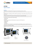
COMMUNICATIONS TEST & MEASUREMENT SOLUTIONS
JD745A
Base Station Analyzer
Spectrum Analyzer: 100 kHz to 4 GHz
Cable and Antenna Analyzer: 5 MHz to 4 GHz
Power Meter: 10 MHz to 4 GHz
Specification Conditions
The JD745A specifications apply under the following conditions.
• After instrument has been turned on for at least 15 minutes.
• The instrument is operating within a valid calibration period.
• Data with no tolerance is considered as typical values.
• The ‘typical’ or ‘nominal’ values are defined as follows:
–– Typical: Expected performance of the instrument operating under 20 to 30°C
after being at this temperature for 15 minutes.
–– Nominal: A general, descriptive term or parameter.
*All specifications subject to change without notice.
Spectrum Analyzer (Standard)
JD745A
Frequency range
100 kHz to 4 GHz
Internal 10 MHz Frequency Reference
Accuracy
±0.05 ppm (25°C ±25°C) + aging
Aging
±0.5 ppm per/year
Frequency Span
Range
Resolution
0 Hz (zero span)
10 Hz to 4 GHz
1 Hz
Resolution Bandwidth (RBW)
–3 dB bandwidth
Accuracy
1 Hz to 3 MHz
1-3-10 sequence
±10% (nominal)
Video Bandwidth (VBW)
–3 dB bandwidth
Accuracy
1 Hz to 3 MHz
1-3-10 sequence
±10% (nominal)
Single Sideband (SSB) Phase Noise
RBW 10 kHz, VBW 1 kHz, RMS detector
Carrier offset:
30 kHz
≤90 dBc/Hz
100 kHz
≤95 dBc/Hz
1 MHz
≤102 dBc/Hz
WEBSITE: www.jdsu.com/test
Typical
JD745A BASE STATION ANALYZER
2
Measurement Range
DANL to +20 dBm
Input attenuator range
Maximum Input Level
Average continuous power
DC voltage
Markers
Marker types
Linear scale and units
Detectors
Number of traces
Trace functions
RF Input VSWR
1.5:1
20 MHz to 4.0 GHz
Typical
+20 dBm
±50 VDC
Displayed Average Noise Level (DANL)
1 Hz RBW, 1 Hz VBW, 50 Ω termination, 0 dB attenuation, RMS detector
Preamplifier Off:
10 MHz to 2.3 GHz
–140 dBm
>2.3 to 3.0 GHz
–138 dBm
>3.0 to 4.0 GHz
–135 dBm
Preamplifier On:
10 MHz to 2.3 GHz
–155 dBm
>2.3 to 3.0 GHz
–153 dBm
>3.0 to 4.0 GHz
–150 dBm
Display Range
Log scale and units
Number of markers
Marker functions
Normal, delta, delta pair noise,
frequency count marker
6
Peak, next peak, peak left,
peak right, minimum search
marker to center/start/stop
0 to 50 dB, 5 dB steps
1 to 20 dB/division in 1 dB steps
10 divisions displayed
dBm, dBV, dBmV, dBµV
10 divisions displayed
V, mV, mW, W
Normal, positive peak, sample,
negative peak, RMS
6
Clear/write, maximum hold,
minimum hold, capture, load
View On/Off
Total Absolute Amplitude Accuracy
Preamplifier off, power level > –50 dBm, auto coupled (25°C ±5°C)
5 MHz to 4 GHz
±1.25 dB, ±0.5 dB (typical) Attenuation < 40 dB
±1.55 dB, ±1.0 dB (typical) Attenuation ≥ 40 dB
Second Harmonic Distortion (Second Harmonic Intercept: SHI)
Mixer level = –25 dBm
10 MHz to 1.3 GHz
< –65 dBc
Typical
1.3 to 4.0 GHz
< –70 dBc
Typical
Third-order Inter-modulation (Third-order Intercept: TOI)
200 MHz to 2 GHz
+10 dBm
Typical
2 to 4 GHz
+12 dBm
Typical
Spurious
Inherent residual response
Input terminated, 0 dB attenuation, preamplifier off, RBW at 10 kHz
20 MHz to 3 GHz
–90 dBm
Nominal
3 to 4 GHz
–85 dBm
Nominal
Exceptions
< –85 dBm at 2497.8 and 1599.0 MHz
Input related spurious
< –70 dBc
Dynamic Range
> 95 dB
Sweep Time
Range
Sweep mode
Reference Level
Setting range
Setting resolution
Log scale
Linear scale
–120 dBm to +100 dBm
0.1 dB
1% of reference level
Gated Sweep
Trigger source
Gate length
Gate delay
Trigger
Trigger source
Trigger delay
Range
Resolution
2/3 (TOI-DANL) in 1Hz RBW
80 ms to 1000 s
24 µs to 200 s
Continuous, single
Span = 0 Hz (zero span)
External
1 µs to 100 ms
0 to 100 ms
Free run, video, external
0 to 200 s
6 µs
JD745A BASE STATION ANALYZER
3
Measurements
Spectrum analysis with CW signal generator
Channel power
Occupied bandwidth
Spectrum emission mask
Adjacent channel power
Spurious emissions
Field strength
AM/FM audio demodulation
Measurements
Reflection (VSWR)
VSWR range
Return loss range
Resolution
Distance to Fault (DTF)
Vertical VSWR range
Vertical return loss range
Vertical resolution
Horizontal range
Cable and Antenna Analyzer (Standard)
General Parameters
Range
Resolution
Accuracy
Data Points
126, 251, 501, 1001
Measurement speed
1 Port measurements
Horizontal resolution
5 MHz to 4 GHz
10 kHz
±25 ppm
1.65 ms/point
Nominal
Measurement Accuracy
Corrected directivity
40 dB (typical)
Reflection uncertainty
0.3 + |20log (1+10-EP/20)| EP = Directivity –
Measured return
loss
Output Power
High
Low
Dynamic Range
Reflection
Maximum Input Level
Average continuous power
DC voltage
Interference immunity
+0 dBm
–30 dBm
Typical
Typical
60 dB
+25 dBm
±50 VDC
+17 dBm on channel
0 dBm on frequency
Nominal
Nominal
Cable Loss (1 port)
Range
Resolution
1-port Phase
Range
Resolution
Smith Chart
Resolution
1 to 65
0 to 60 dB
0.01
1 to 65
1 to 60 dB
0.01
0 to (# of data
points – 1) x
horizontal resolution
(1.5x10⁸)x(Vp)/
(Delta)x(0.95)
Maximum = 1500 m
(4921 ft)
Vp = Propagation velocity
Delta = Stop Freq – Start
Freq [Hz]
0 to 30 dB
0.01 dB
–180° to +180°
0.01°
0.01
Power Meter (Standard)
General Parameters
Display range
Offset range
Resolution
–100 to +100 dBm
0 to 60 dB
0.01 dB or 0.1xW
Internal Power Sensor
Frequency range
Span
Dynamic range
Maximum power
Accuracy
10 MHz to 4 GHz
100 kHz to 100 MHz
–120 to +20 dBm
+20 dBm
Same as spectrum analyzer
x = m, u, p
JD745A BASE STATION ANALYZER
4
External Power Sensors
Directional power sensors
Frequency range
Dynamic range
Connector type
Measurement type
Accuracy
JD731A
JD733A
300 to 3800 MHz
150 to 3800 MHz
Average
0.15 to 150 W
Average
Peak
4 to 400 W
Peak
Type N (f ) on both ends
Forward/reverse average power, forward peak power, VSWR
±4% + 0.05 W1
Terminating power sensors
Frequency range
Dynamic range
Connector type
Measurement type
Accuracy
JD732A
20 to 3800 MHz
–30 to 20 dBm
Type N (m)
Average
±7%1
Optical power meter
Display range
–100 to +100 dBm
Offset range
Resolution
0 to 60 dB
0.01 dB or 0.1 mW
External optical power sensors
Optical power sensors
Wavelength range
Max permitted input level
Connector input
Accuracy
CW condition at 25°C ±10°C
1
MP-60
+10 dBm
Universal 2.5 and 1.25 mm connectors
JD734A
20 to 3800 MHz
–30 to 20 dBm
Type N (m)
Peak
±7%1
0.1 to 50 W
0.1 to 50 W
JD736A
20 to 3800 MHz
–30 to 20 dBm
Type N (m)
Average and peak
±7%1
MP-80
780 to 1650 nm
+23 dBm
±5%
JD745A BASE STATION ANALYZER
5
2-Port Transmission Measurements (Option 001)
Frequency
Frequency range
Frequency resolution
GPS Receiver and Antenna (Option 010)
GPS Indicator
Latitude, Longitude, Altitude
5 MHz to 4 GHz
10 kHz
High-frequency Accuracy
Output Power
High
Low
Measurement Speed
2.2 ms/point
Dynamic Range
Vector:
Scalar:
Measurements
Insertion Loss/Gain
Range
Resolution
2-port Phase
Range
Resolution
0 dBm
–30 dBm
Typical
Typical
Spectrum, interference, and
signal analyzer
GPS lock
Hold over
Connector
±25 ppb
±50 ppb
SMA, female
15 minutes after locking to GPS
Nominal
Interference Analyzer (Option 011)
5 MHz to 3 GHz, 80 dB
> 3 to 4 GHz, 75 dB
5 MHz to 4 GHz >100 dB
–120 to 100 dB
0.01 dB
–180° to +180°
0.01°
Measurements
Spectrum analyzer
Spectrogram
RSSI
Sound indicator, AM/FM audio demodulator,
interference ID, spectrum recorder
Collect data up to 72 hours
Collect data up to 72 hours Received signal
strength indicator
Interference finder
Spectrum player
Channel Scanner (Option 012)
Frequency Range
100 kHz to 4 GHz
Bias Tee (Option 002)
Voltage
Voltage range
Voltage resolution
Power
8 W Max
+12 to +32 V
0.1 V
10 MHz to 4 GHz
CW Signal Generator (Option 003)
Frequency
Frequency range
Frequency reference
Frequency resolution
25 MHz to 4 GHz
< ±25 ppm
10 kHz
Output Power
Range
Step
Accuracy
0 dBm, –30 to –80 dBm
1 dB
±1.5 dB
Measurement Range
–110 to +20 dBm
Measurements
Channel scanner
Frequency scanner
Custom scanner
1 to 20 channels
1 to 20 frequencies
1 to 20 channels or frequencies
JD745A BASE STATION ANALYZER
6
GSM/GPRS/EDGE Signal Analyzer (Option 022)
General Parameters
Frequency range
Input signal range
Burst power
Frequency error
GMSK modulation quality
Phase RMS accuracy
Residual error
Phase peak accuracy
8 PSK modulation quality
EVM accuracy
Residual error
RF power vs time
450 to 500 MHz
820 to 965 MHz
1705 to 1995 MHz
–40 to +20 dBm
±1.0 dB
±10 Hz + ref freq accuracy
±1.0 degrees
99% Confidence level
(0 < Phase RMS < 8)
0.7 degrees
±2.0 degrees
±1.5%
Typical
(0 < Phase peak < 30)
(2% < EVM < 8%)
2.5%
±0.25 symbol
Measurements
Channel power
Channel power
Spectral density
Peak to average power
Occupied bandwidth
Occupied bandwidth
Integrated power
Occupied power
Spectrum emission mask
Reference power
Peak level at defined range
Spurious emissions
Peak frequency at defined range
Peak level at defined range
Option 022
Power vs. time (Slot)
Burst power
Max/Min point
Power vs. time (Frame)
Frame average power
Burst power (Slot 0 to 7)
TSC (Slot 0 to 7)
Constellation
Burst power
Modulation type
Frequency error
Phase error RMS
Phase error peak
IQ origin offset*
TSC
BSIC
C/I*
EVM RMS*
EVM Peak*
EVM 95th*
Auto measure
Channel power
Occupied bandwidth
Spectrum emission mask
Burst power
Frame average power
PvsT – Mask
Frequency error
Phase error RMS
Phase error peak
EVM RMS*
EVM Peak*
IQ origin offset
C/I*
* The measurements are performed for 8 PSK modulation signals (EDGE) only.
Longitude, latitude, and satellite in all screens
Option 042
Channel scanner
Frequency scanner
Absolute power
Group (Traffic, Control)
BSIC (NCC, BCC)
Multipath profile
(Ten strongest)
Frame average power
SNR, delay
Modulation analyzer
Frame avg power trend
C/I trend
Frame average power
BSIC, frame No. and time
C/I, frequency error
Burst power
Modulation type
JD745A BASE STATION ANALYZER
7
WCDMA/HSDPA Signal Analyzer (Option 023 for WCDMA, Option 024 for HSDPA)
General Parameters
Frequency range
Input signal range
RF channel power accuracy
Occupied bandwidth accuracy
Adjacent channel leakage ratio
(ACLR)
WCDMA modulation
HSDPA modulations
Frequency error
EVM accuracy
Residual EVM
Code domain power
CPICH accuracy (dBm)
Band I to Band XIV
–40 to +20 dBm
±1.0 dB, ±0.7 dB (typical)
±100 kHz
< –56 dB, ±0.7 dB at 5 MHz offset
< –58 dB, ±0.8 dB at 10 MHz offset
QPSK
QPSK, 16 QAM, 64 QAM
±10 Hz + ref freq accuracy
±2.0%, 2% ≤ EVM ≤ 20%
2.5%
±0.5 dB relative power
±1.5 dB absolute power
±0.8 dB
99% Confidence level
Typical
Code channel power > –25 dB
Typical
Measurements
Channel power
Channel power
Spectral density
Peak to average power
Occupied bandwidth
Occupied bandwidth
Integrated power
Occupied power
Spectrum emission mask
Reference power
Peak level at defined range
ACLR
Reference power
Abs power at defined range
Rel power at defined range
Multi-ACLR
Lowest reference power
Highest reference power
Abs power at defined range
Rel power at defined range
Spurious emissions
Peak Freq at defined range
Peak Level at defined range
Option 023 and 024
Constellation
Auto measure
CPICH power
Channel power
Rho, EVM
Occupied bandwidth
Peak CDE
Spectrum emission mask
Frequency error
ACLR
Time offset
Multi-ACLR
Carrier feed through
Frequency error
Scramble Code
EVM
Code domain power
Peak CDE
Abs/Rel code power
Carrier feed through
Individual code EVM,
CPICH absolute power
Constellation
CPICH relative power
Channel power
Max inactive power
Power bar graph
(Abs/Rel/delta power)
Power statistics CCDF
CPICH, PCCPCH, SCCPCH
PICH, P-SCH, S-SCH
Max, avg active power
Max, avg inactive power
Scramble code
Codogram
Code utilization
RCSI
CPICH, P-CCPCH, S-CCPCH,
PICH, P-SCH, S-SCH
CDP table
Code utilization
Code, spreading exactor
Allocation (channel type)
EVM, modulation type
Relative, absolute power
Longitude, latitude, and satellite in all screens
Option 043
Channel scanner (up to 6)
Frequencies or channels
Channel power, scramble
Code, CPICH power, Ec/Io
Scramble scanner (up to 6)
Channel power
CPICH dominance
Scramble code
Ec/Io, CPICH power, delay
Multipath profile
Channel, multipath power
Ec/Io, delay
Code domain power
Abs/Rel code power
Individual code EVM
Channel power
Scramble code
CPICH, PCCPCH, SCCPCH,
PICH, P-SCH, S-SCH power
Max, avg active power
Max, avg inactive power
Frequency error
Time offset, Rho
Carrier feed through
(Composite) EVM
CPICH EVM, P-CCPCH EVM
Amplifier capacity
Peak amplifier capacity
Average amplifier capacity
Code, peak utilization
Average utilization
JD745A BASE STATION ANALYZER
8
cdmaOne/CDMA2000 Signal Analyzer (Option 020)
General Parameters
Frequency range
Input signal level
RF channel power accuracy
CDMA compatibility
Frequency error
Rho accuracy
Residual Rho
PN offset
Code domain power
Pilot power accuracy
Time offset
Band 1 to Band 10
–40 to +20 dBm
±1.0 dB
cdmaOne and CDMA2000
±10 Hz + ref freq accuracy
±0.005, 0.9 < Rho < 1.0
>0.995
1 x 64 chips
±0.5 dB relative power
±1.5 dB absolute power
±1.0 dB
±1.0 μs, ±0.5 μs (typical)
Typical
99% Confidence level
Typical
External trigger
Measurements
Channel power
Channel power
Spectral density
Peak to average power
Occupied bandwidth
Occupied bandwidth
Integrated power
Occupied power
Spectrum emission mask
Reference power
Peak level at defined range
ACPR
Reference power
Abs power at defined range
Rel power at defined range
Multi-ACPR
Lowest reference power
Highest reference power
Abs power at defined range
Rel power at defined range
Spurious emissions
Peak freq at defined range
Peak level at defined range
Option 020
Constellation
Pilot power
Rho
EVM
Frequency error
Time offset
Carrier feed through
Pn offset
Code domain power
Abs/Rel code power
Channel power
Power bar graph (Abs/Rel)
Pilot, sync
Page, Q-page
Max, avg active power
Max, avg inactive power
PN offset
Codogram
Code Utilization
RCSI
Pilot, paging, sync, Q-page
CDP table
Code utilization
Code, spreading factor
Allocation (channel type)
Relative, absolute power
Auto measure
Channel power
Occupied bandwidth
Spectrum emission mask
ACLR
Multi-ACLR
Rho
Frequency error
Time offset
Carrier feed through
Pilot power
Max inactive power
Power statistics CCDF
Longitude, latitude, and satellite in all screens
Option 040
Channel scanner (up to 6)
Frequencies or channels
Channel power, PN offset
Pilot power, Ec/Io
PN scanner (up to 6)
Channel power
Pilot dominance
PN offset
Ec/Io, pilot power, delay
Multipath profile
Channel power
Multipath power
Ec/Io, delay
Code domain power
Abs/Rel code power
Channel power
Pn offset
Pilot, sync power
Page, Q-page power
Max, avg active power
Max, avg inactive power
Frequency error
Time offset, Rho, EVM
Carrier feed through
Amplifier capacity
Peak amplifier capacity
Average amplifier capacity
Code, peak utilization
Peak utilization
Average utilization
JD745A BASE STATION ANALYZER
9
EV-DO Signal Analyzer (Option 021)
General Parameters
Frequency range
Input signal level
RF channel power accuracy
EV-DO compatibility
Frequency error
Rho accuracy
Residual Rho
PN offset
Code domain power
Pilot power accuracy
Time offset
Band 1 to Band 10
–40 to +20 dBm
±1.0 dB
Rev 0, Rev A and Rev B
±10 Hz + ref freq accuracy
±0.005, 0.9 < Rho < 1.0
>0.995
1 x 64 chips
±0.5 dB relative power
±1.5 dB absolute power
±1.0 dB
±1.0 μs, ±0.5 μs (typical)
Typical
99% Confidence level
Typical
External trigger
Measurements
Channel power
Channel power
Spectral density
Peak to average power
Occupied bandwidth
Occupied bandwidth
Integrated power
Occupied power
Spectrum emission mask
Reference power
Peak level at defined range
ACPR
Reference power
Abs power at defined range
Rel power at defined range
Multi-ACPR
Lowest reference power
Highest reference power
Abs power at defined range
Rel power at defined range
Spurious emissions
Peak frequency at defined range
Peak level at defined range
Option 021
Power vs. time
MAC codogram
(idle and active slot)
Code utilization
Slot average power
RCSI
On/Off Ratio
Slot, pilot, MAC, data
Idle activity
MAC CDP table
Pilot, MAC, data power
Code utilization
Constellation
Code, spreading factor
(Composite 64/128, pilot,
Allocation (channel type)
MAC 64/128, data)
Relative, absolute power
Channel power
Rho, EVM
Auto measure
Peak CDE
Channel power
Frequency error
Occupied bandwidth
Time offset
Spectrum emission mask
Carrier feed through
ACLR
PN offset
Multi-ACLR
Data modulation type*
Pilot, MAC, data power
Code domain power
On/Off ratio
(Pilot and MAC 64/128)
Pvst mask (idle slot)
Pilot power/MAC power
Pvst mask (active slot)
Slot average power
Frequency error
Max, Avg Active I/Q pwr
Time offset
Max, Ave Inactive I/Q pwr
Carrier feed through
PN offset
Pilot, MAC, data Rho
Code domain power (data)
PN offset
Data power
Slot average power
Power statistics CCDF
Max, avg active power
Max, avg inactive power
PN offset
Longitude, latitude, and satellite in all screens
Option 041
Channel scanner (up to 6)
Frequencies or channels
Pn offset
Pilot, MAC, data power
PN scanner (up to 6)
Channel power
Pilot dominance
PN offset
Ec/Io, pilot power, delay
Multipath profile
Channel power
Multipath power
Ec/Io, delay
Code domain power
Slot average power
PN offset
Pilot, MAC, data power
Pilot, MAC, data Rho
(composite) EVM
Frequency error
Time offset
Carrier feed through
Max active I/Q power
Avg active I/Q power
Code utilization
Peak utilization
Average utilization
JD745A BASE STATION ANALYZER
10
TD-SCDMA Signal Analyzer (Option 025)
General Parameters
Frequency range
Input signal level
Channel power (RRC) accuracy
Modulations
Frequency error
Residual EVM (RMS)
Time error (Tau)
Spreading factor
1785 to 2220 MHz
–40 to +20 dBm
±1.0 dB
QPSK, 8 PSK, 16 QAM, 64 QAM
±10 Hz + ref freq accuracy
2.0% typical
±0.2 μs (typical)
Auto (DL, UL), 1, 2, 4, 8, 16
Typical
99% Confidence level
P-CCPCH slot and 1 channel
External trigger
JD745A BASE STATION ANALYZER
11
Measurements
Channel power
Channel power
Spectral density
Peak to average power
Occupied bandwidth
Occupied bandwidth
Integrated power
Occupied power
Spectrum emission mask
Reference power
Peak Level at defined range
ACLR
Reference power
Abs Power at defined range
Rel Power at defined range
Multi-ACLR
Lowest reference power
Highest reference power
Abs power at defined range
Rel power at defined range
Spurious emissions
Peak frequency at defined range
Peak level at defined range
Option 025
Power vs. time (slot)
Code error
Slot power
Code power
DwPTS power
Code error
UpPTS power
Individual code EVM
On/Off slot ratio
Individual code constellation
Slot pAR
Data Format
DwPTS code
Slot, DwPTS power
Power vs. time (frame)
No. of active code
Slot power (TS 0 to 6)
Scramble code
Data power left (TS 0 to 6)
Max active code power
Midamble power (TS 0 to 6)
Avg active code power
Data power right (TS 0 to 6)
Max inactive code power
Time offset (TS 0 to 6)
Avg inactive code power
Power vs. time (mask)
Peak CDE
Slot power
Peak active CDE
On/Off slot ratio
Off power
Timogram
Auto measure
Constellation
Channel power
Rho
Occupied bandwidth
EVM RMS, EVM peak
Spectrum emission mask
Peak CDE
ACLR
Frequency error
Multi-ACLR
IQ origin offset
Slot power
Time Offset
DwPTS power
Midamble power
UpPTS power
Slot power
On/Off slot ratio
DwPTS power
EVM RMS
Midamble power (1 to 16)
PCDE
Code power
Frequency error
Abs/Rel code power
Max inactive power
Individual code EVM,
Scramble code
Individual code constellation
Data format
Slot power, DwPTS power
No. of active code
Scramble code
Max active code power
Avg active code power
Max inactive code power
Avg inactive code power
Longitude, latitude, and satellite in all screens
Option 045
Sync-DL ID scanner (32)
Scramble code group
Ec/Io, Tau
DwPTS power
Pilot dominance
Sync-DL ID vs. Tau (up to 6)
ID, power, Ec/Io, Tau
DwPTS power
Pilot dominance
Sync-DL ID multipath
Ec/Io, Tau
DwPTS power
Pilot dominance
Sync-DL ID analyzer
DwPTS power, Ec/Io trend
DwPTS power
Pilot dominance
EVM, frequency error
Ec/Io, CINR
JD745A BASE STATION ANALYZER
12
Mobile WiMAX Signal Analyzer (Option 026)
General Parameters
Frequency range
Input signal level
Channel power accuracy
Supported bandwidth
Frequency error
Residual EVM (RMS)
2100 to 2700 MHz
3400 to 3850 MHz
–40 to +20 dBm
±1.0 dB
7, 8.75, and 10 MHz
±10 Hz + ref freq accuracy
1.5% typical
Typical
99% Confidence level
Measurements
Channel power
Channel power
Spectral density
Peak to average power
Occupied bandwidth
Occupied bandwidth
Integrated power
Occupied power
Spectrum emission mask
Reference power
Peak level at defined range
Spurious emissions
Peak frequency at defined range
Peak level at defined range
Option 026
Power vs. time (frame)
Auto measure
Channel power
Channel power
Frame average power
Occupied bandwidth
Preamble power
Spectrum emission mask
DL burst power
Preamble power
UL burst power
DL Burst power
IQ origin offset
UL Burst power
Time offset
Frame average power
Constellation
Time offset
Channel power
IQ origin offset
RCE RMS, RCE peak
Spectral flatness
EVM RMS, EVM peak
Frequency error
Frequency error
RCE RMS
Time offset
RCE peak
Segment ID, cell ID
EVM RMS
Preamble index
EVM peak
Spectral flatness
Average subcarrier power
Power statistics CCDF
Subcarrier Pwr variation
Max, min, avg power
EVM vs. subcarrier
RCE RMS, RCE peak
EVM RMS, EVM peak
Segment ID, cell ID
Preamble index
EVM vs. symbol
RCE RMS, RCE peak
EVM RMS, EVM peak
Segment ID, cell ID
Preamble index
Longitude, latitude, and satellite in all screens
Option 046
Preamble scanner (up to 6)
Total preamble power
Preamble, relative power
Cell ID, sector ID
Time offset
Multipath profile
Total preamble power
Multipath power
Preamble power, delay
Preamble power trend
Preamble power trend
Relative power trend
Preamble power
Frame avg power
Relative power
C/I
Preamble
Cell ID, sector ID
Time offset
JD745A BASE STATION ANALYZER
13
LTE-FDD Signal Analyzer (Option 028)
General Parameters
Frequency range
Input signal level
Channel power accuracy
Supported bandwidth
Frequency error
Residual EVM (RMS)
Band 1 to 19
–40 to +20 dBm
±1.0 dB
1.4, 3, 5, 10, 15, and 20 MHz
±10 Hz + ref freq accuracy
2.0% typical
Typical
99% Confidence level
Data EVM
JD745A BASE STATION ANALYZER
14
Measurements
Channel power
Channel power
Spectral density
Peak to average power
Occupied bandwidth
Occupied bandwidth
Integrated power
Occupied power
Spectrum emission mask
Reference power
Peak level at defined range
ACLR
Reference power
Abs power at defined range
Rel power at defined range
Spurious emissions
Peak frequency at defined range
Peak level at defined range
Multi-ACLR
Lowest reference power
Highest reference power
Abs power at defined range
Rel power at defined range
Spurious emissions
Peak frequency at defined range
Peak level at defined range
Power vs. time (frame)
Frame average power
Subframe power
First slot power
Second slot power
Cell ID, IQ origin offset
Time offset
Constellation
RS TX power
PDSCH QPSK EVM
PDSCH QPSK EVM
PDSCH QPSK EVM
Data EVM RMS
Data EVM peak
Frequency error
Time error
Option 028
Data channel
Time alignment error
Resource block power
Time alignment error trend
IQ diagram
Time alignment error
RB power
RS power difference
Modulation format
Antenna 0 RS power
IQ origin offset
Antenna 0 RS EVM
EVM RMS, EVM peak
Antenna 1 RS power
Control channel
Antenna 1 RS EVM
Control channels table
Data allocation map
(P-SS, S-SS, PBCH,
Data allocation vs frame
PCFICH, PHICH, PDCCH, RS)
Resource block power
EVM, relative or absolute power,
OFDM symbol power
mod type control channel metrics
Data utilization
IQ diagram, modulation format
Data allocation vs subframe
frequency error
Resource block power
IQ origin offset
Data utilization
EVM RMS, EVM peak
Subframe summary
Auto measure
Subframe summary table
Channel power
(P-SS, S-SS, PBCH, PCFICH, PHICH,
Occupied bandwidth
PDCCH, RS, PDSCH QPSK, 16, 64QAM) Spectrum emission mask
EVM, relative or
ACLR
absolute power, mod type
IQ origin offset
Subframe power
Time error
OFDM symbol power
EVM RMS
Frequency error
Data EVM peak
Time offset
Frequency error
Data EVM RMS, peak
RS power
RS EVM RMS, peak
P-SS power
Frame summary
S-SS power
Frame summary table
PBCH power
(P-SS, S-SS, PBCH,
PCFICH power
PCFICH, PHICH, PDCCH, RS,
PDSCH QPSK, 16, 64QAM)
Power statistics CCDF
EVM, relative or absolute power,
modulation type
Frame average power
OFDM symbol power
Frequency error
IQ origin offset
EVM RMS, peak
Data EVM RMS, peak
Longitude, latitude, and satellite in all screens
Option 048
ID scanner (up to 6)
P-SS dominance
S-SS dominance
Cell, group, sector ID
P-SS, S-SS power
P-SS, S-SS Ec/Io
Multipath profile
Cell, group, sector ID
P-SS Ec/Io, delay
S-SS Ec/Io, delay
Control channel
RS power trend
Cell, group, sector ID
control channel table
(P-SS, S-SS, PCFICH, RS 0, RS 1)
Absolute power
Relative power
EVM RSM, peak
Frequency error
Time alignment error
Datagram
Datagram
Resource block power
Data utilization
JD745A BASE STATION ANALYZER
15
LTE-FDD Signal Analyzer (Option 029)
General Parameters
Frequency range
Input signal level
Channel power accuracy
Supported bandwidth
Frequency error
Residual EVM (RMS)
Band 33 to band 40
–40 to +20 dBm
±1.0 dB
1.4, 3, 5, 10, 15, and 20 MHz
±10 Hz + Ref freq accuracy
2.0% (Typical)
Typical
99% Confidence level
Data EVM
Measurements
Channel power
Channel power
Spectral density
Peak to average power
Occupied bandwidth
Occupied bandwidth
Integrated power
Occupied power
Spectrum emission mask
Reference power
Peak level at defined range
ACLR
Reference power
Abs power at defined range
Rel power at defined range
Spurious emissions
Peak frequency at defined range
Peak level at defined range
Power vs. time (frame)
Frame average power
Subframe power
First slot power
Second slot power
Cell ID, IQ origin offset
Time offset
Power vs. time (slot)
Slot average power
Transient period length
Off power
Option 029
Constellation
RS TX power
PDSCH QPSK EVM
PDSCH QPSK EVM
PDSCH QPSK EVM
Data EVM RMS
Data EVM peak
Frequency error
Time error
Data channel
Resource block power
IQ diagram
RB power
Modulation format
IQ origin offset
EVM RMS, EVM peak
Control channel
Control channel table
(P-SS, S-SS, PBCH,
PCFICH, PHICH, PDCCH, RS)
EVM, relative or absolute power
modulation type
Each control channels’
IQ diagram
Modulation format
Frequency error
Time alignment error
Time alignment error trend
Time alignment error
RS power difference
Antenna 0 RS power
Antenna 0 RS EVM
Antenna 1 RS power
Antenna 1 RS EVM
Auto measure
Channel power
Occupied bandwidth
Spectrum emission mask
ACLR
IQ origin offset
Time error
EVM RMS
Data EVM peak
Frequency error
RS power
P-SS power
S-SS power
PBCH power
PCFICH power
Power statistics CCDF
IQ origin offset
EVM RMS, EVM peak
Subframe summary
Summary table
(P-SS, S-SS, PBCH, PCFICH, PHICH,
PDCCH, RS, PDSCH QPSK, 16, 64QAM)
EVM, relative or absolute power,
modulation type
Subframe power
OFDM symbol power
Frequency error
Time offset
Data EVM RMS, peak
RS EVM RMS, peak
Longitude, latitude, and satellite in all screens
Option 049
ID scanner (up to 6)
P-SS dominance
S-SS dominance
Cell, group, sector ID
P-SS, S-SS power
P-SS, S-SS Ec/Io
Multipath profile
Cell, group, sector ID
P-SS Ec/Io, delay
S-SS Ec/Io, delay
Control channel
RS power trend
Cell, group, sector ID
Control channel table
(P-SS, S-SS, PCFICH,
RS, PBCH)
Absolute power
Relative power
EVM RSM, peak
Frequency error
Datagram
Datagram
Resource block power
Data utilization
JD745A BASE STATION ANALYZER
16
E1 Analyzer (Option 004)
Electrical Interface
Connectors RX/TX
Output
Line code
Impedance
Input
Term/Bridge/Monitor
RJ48C (120 Ω)
0 dB, -6 dB (ITU-T Rec.G.703)
AMI, HDB3
Term, monitor 120 Ω,
Bridge > 1000 Ω
Electrical Interface
Connectors RX/TX
Output
Line code
Impedance
RJ48C (120 Ω)
0, –7.5 and –15 dB
AMI, HDB3
100 Ω or 1000 Ω (Bridge)
Input
Term/Bridge/Monitor
0 to −20 dB
0 to −20 dB
Transmitter and Receiver
Framing
PCM-30, PCM-30 with CRC
PCM-31, PCM-31 with CRC
Channel formats
Full E1
Test pattern
1-4, 1-8, ALL1, ALL0, 0101
Additional Functions
Reference clock
Event log capability
Error insertion
Error rate count
T1 Analyzer (Option 005)
Received or internal
Internal memory
1, 1E–3, 1E–4, 1E–5
CRC, frame, code, bit
Measurements
Option 002
Monitoring/error injection
Indicators
E1 signal
Frame sync
Pattern sync
Code sync
FAS RAI
AIS
HDB8
Error count/rate
CRC error
When CRC-4 is set to On
Frame error
Code error
Bit error
When PCM31 is set to On
Alarm count
FAS
AIS
Loss count
Frame sync
Pattern sync
Transmitter and Receiver
Framing
D4, ESF
Channel formats
Full E1
Test pattern
1–8, 1–16, ALL1, ALL0, 0101
2E–24, QRSS, 2E–23, 2E–15
2E–23 Inverse, 2E–15 Inverse
Additional Functions
Reference clock
Event log capability
Error insertion
Alarm insertion
Error/alarm count
Loopback modes
Measurements
Option 003
Monitoring/BERT/loop test
Indicators
T1 signal loss
Frame sync
Pattern sync
B8ZS
Loss count
Signal loss
Frame sync loss
Alarm count
RAI
AIS
Error rate
Bit error rate
RX signal level
Indicators
T1 signal loss
Frame sync
Pattern sync
B8ZS
Red alarm
RAI (yellow alarm)
Received or internal
Internal memory
1, 1E–3, 1E–4, 1E–5
AIS, RAI
Bit RAI, AIS, BPV, BER
Self, CSU, NIU, line, network
Red alarm
RAI (yellow alarm)
AIS (blue alarm)
BPV indicator
Pattern sync loss
BPV
Bit error count
AIS (blue alarm)
BPV indicator
Vp-p
Vp-p Max
Vp-p Min
dBdsx
JD745A BASE STATION ANALYZER
17
General Information
Inputs and Outputs
RF in
Connector
Impedance
Damage level
Reflection/RF out
Connector
Impedance
Damage level
RF in
Connector
Impedance
Maximum level
External trigger, GPS
Connector
Impedance
External ref
Connector
Impedance
Input frequency
Input range
USB
USB host
USB client
LAN
E1/T1
Audio jack
External power
Speaker
Battery
Spectrum analyzer
Type-N, female
50 Ω (nominal)
> +40 dBm, > ±50 VDC
Nominal
Cable and antenna analyzer
Type-N, female
50 Ω (nominal)
> +37 dBm, > ±50 VDC Nominal
Cable and antenna analyzer
Type-N, female
50 Ω (nominal)
> +25 dBm, > ±50 VDC
Operating time
Charge time
Storage temperature
SMA, female
50 Ω (nominal)
Data Storage
Internal
SMA, female
50 Ω (nominal)
10, 13, 15 MHz
–5 dBm to +5 dBm
Environmental
Operating temperature
Maximum humidity
Shock and vibration
Storage temperature
(With the battery pack
removed)
EMC
EN 61326-2-1
8 in, LED backlight
800 x 600
Power
External DC input
Power consumption
12 to 19 VDC
32.5 W
Minimum 20 MB
External
Type A, 1 port
Connects flash drive and power sensor
Type B, 1 port
Connects to PC for data transfer
RJ45, 10/100 Base-T
Connects to PC for data transfer
RJ48C
3.5 mm headphone jack
5.5 mm barrel connector
Built-in speaker
Display
Size
Resolution
10.8 V, 7200 mA/hr Lithium ion
> 3 hours typical
A fully discharged
battery takes about
2.5 hours to recharge
to 80%, 4 hours to
100%
–10 to 60°C, ≤85% RH Store battery pack in
14 to 140°F, ≤85% RH low-humidity environment. Extended
exposure to temperatures above
45°C could degrade
battery performance
and life.
–10 to 55°C (14 to 131°F)
85%
MIL-PRF-28800F Class 2
–55 to 71°C (–67 to 160°F)
Complies with European EMC
Safety
EN 61010-1 2nd
45 W maximum
(when charging battery)
Size and Weight (Standard configuration)
Weight with battery
< 4 kg (8.8 lbs)
Size (W x H x D)
295 x 195 x 82 mm
(11.6 x 7.7 x 3.2 in)
Warranty
2 years
Calibration Cycle
1 year
Up to 200 instrument
states and trace
Supports USB 2.0
compatible memory
devices
JD745A BASE STATION ANALYZER
18
Ordering Information
JD745A Base Station Analyzer
100 kHz to 4 GHz Spectrum Analyzer
5 MHz to 4 GHz
Cable and Antenna Analyzer1
10 MHz to 4 GHz RF Power Meter (internal mode)
Options
NOTE: Upgrade options for the JD745A use the designation JD745AU
before the respective last three-digit option number.
JD745A001
2-Port Transmission Measurement2
JD745A002
Bias Tee (Requires option 01)
JD745A003
CW Signal Generator
JD745A004
E1 Analyzer3
JD745A005
T1 Analyzer3
JD745A010
GPS Receiver and Antenna
JD745A011
Interference Analyzer 3,4
JD745A012
Channel Scanner
JD745A013
Optical Power Meter (Requires optical power sensor)
JD745A020
cdmaOne/CDMA2000 Signal Analyzer
JD745A021
EV-DO Signal Analyzer (Requires option 20)
JD745A022
GSM/GPRS/EDGE Signal Analyzer
JD745A023
WCDMA Signal Analyzer
JD745A024
HSDPA Signal Analyzer (Requires option 23)
JD745A025
TD-SCDMA Signal Analyzer
JD745A026
Mobile WiMAX Signal Analyzer
JD745A028
LTE-FDD Signal Analyzer
JD745A029
LTE-TDD Signal Analyzer
JD745A040
cdmaOne/CDMA2000 OTA Analyzer (Requires
option 10)
JD745A041
EV-DO OTA Analyzer (Requires option 10)
JD745A042
GSM/GPRS/EDGE OTA Analyzer (Requires option 10)
JD745A043
WCDMA/HSDPA OTA Analyzer (Requires option 10)
JD745A045
TD-SCDMA OTA Analyzer (Requires option 10)
JD745A046
Mobile WiMAX OTA Analyzer (Requires option 10)
JD745A048
LTE-FDD OTA Analyzer (Requires option 10)
JD745A049
LTE-TDD OTA Analyzer (Requires option 10)
Requires Calibration Kit
Requires Dual-Port Calibration Kit
Requires Test Cable
4
Highly recommend adding JD745A010
5
Highly recommend adding G70005035x and/or G70005036x
6
Standard accessories can be purchased separately.
1
2
3
Standard Accessories
G710550322
AC/DC Power Adapter6
G710550335
Cross LAN Cable (1.5 m)6
GC73050515
USB A to B Cable (1.8 m)6
GC72450518
> 1 G Byte USB Memory6
G710550325
Rechargeable Lithium Ion Battery6
G710550323
Automotive Cigarette Lighter 12 VDC Adapter6
JD745A361
JD745A User’s Manual and Application Software – CD
Optional Power Sensors
JD731A
Directional Power Sensor (peak and average power)
Frequency: 300 MHz to 3.8 GHz
Power: Average 0.15 to 150 W, Peak 4 to 400 W
JD733A
Directional Power Sensor (peak and average power)
Frequency: 150 MHz to 3.5 GHz
Power: Average/Peak 0.1 to 50 W
JD732A
Terminating Power Sensor (average power)
Frequency: 20 MHz to 3.8 GHz
Power: –30 to 20 dBm
JD734A
Terminating Power Sensor (peak power)
Frequency: 20 MHz to 3.8 GHz
Power: –30 to 20 dBm
JD736A
Terminating Power Sensor (peak and average
power)
Frequency: 20 MHz to 3.8 GHz
Power: –30 to 20 dBm
Optional Optical Power Sensors
MP-60
Miniature USB 2.0 Optical Power Sensor
Wavelength range: 780 to 1650 nm
1300, 1310, 1490, 1550 nm: –50 to +10 dBm
850 nm: –45 to +10 dBm
MP-80
Miniature USB 2.0 Optical Power Sensor
Wavelength range: 780 to 1650 nm
1300, 1550 nm: –35 to +23 dBm
850 nm: –30 to +23 dBm
JD745A BASE STATION ANALYZER
19
Ordering Information (cont'd)
Optional Calibration Kits
JD72450509
One-Port N-Type Calibration Kit Open/Short/Load
N(m), 40 dB, 4 GHz, 50 Ω
JD72450510
One-Port DIN-Type Calibration Kit Open/Short/
Load DIN(m), 40 dB, 4 GHz, 50 Ω
JD71050507
Dual-Port N-Type Calibration Kit, 50 Ω
• Open/Short/Load N(m), 40 dB, 4 GHz, 50 Ω
• Two Adapters N(f ) to N(f ), DC to 4 GHz, 50 Ω
• Two 1 m (3.28 ft) RF Test Cables, N(m) to N(m),
DC to 18 GHz, 50 Ω
JD71050508
Dual-Port DIN-Type Calibration Kit, 50 Ω
• Open/Short/Load DIN(m), 40 dB, 4 GHz, 50 Ω
• Two 1 m (3.28 ft) RF Test Cables, N(m) to N(m),
DC to 18 GHz, 50 Ω
• Adapter N(f ) to DIN(f ), DC to 4 GHz, 50 Ω
• Adapter N(f ) to DIN(m), DC to 4 GHz, 50 Ω
• Adapter DIN(f ) to DIN(f ), DC to 4 GHz, 50 Ω
• Adapter DIN(m) to DIN(m), DC to 4 GHz, 50 Ω
Optional RF Cables
G710050530
1.0 m (3.28 ft) RF Cable, DC to 18 GHz, N(m)-N(m), 50 Ω
G710050531
1.5 m (4.92 ft) RF Cable, DC to 18 GHz, N(m)-N(f ), 50 Ω
G710050532
3.0 m (9.84 ft) RF Cable, DC to 18 GHz, N(m)-N(f ), 50 Ω
Optional Omni Antennas
G700050351
RF Omni Antenna 400 MHz to 450 MHz
G700050352
RF Omni Antenna 450 MHz to 500 MHz
G700050353
RF Omni Antenna 806 MHz to 896 MHz
G700050354
RF Omni Antenna 870 MHz to 960 MHz
G700050355
RF Omni Antenna 1710 MHz to 2170 MHz
G700050356
RF Omni Antenna 720 to 800 MHz
Optional Yaggi Antennas
G700050364
RF Yaggi Antenna 806 MHz to 896 MHz
G700050365
RF Yaggi Antenna 866 MHz to 960 MHz
G700050363
RF Yaggi Antenna 1750 MHz to 2390 MHz
Optional Adapters
G710050571
Adapter N(m) to DIN(f ), DC to 4 GHz, 50 Ω
G710050572
Adapter DIN(m) to DIN(m), DC to 4 GHz, 50 Ω
G710050573
Adapter N(m) to SMA(f ), DC to 18 GHz, 50 Ω
G710050574
Adapter N(m) to BNC(f ), DC to 1.5 GHz, 50 Ω
G710050575
Adapter N(f ) to N(f ), DC to 4 GHz, 50 Ω
G710050576
Adapter N(m) to DIN(m), DC to 4 GHz, 50 Ω
G710050577
Adapter N(f ) to DIN(f ), DC to 4 GHz, 50 Ω
G710050578
Adapter N(f ) to DIN(m), DC to 4 GHz, 50 Ω
G710050579
Adapter DIN(f ) to DIN(f ), DC to 4 GHz, 50 Ω
Optional E1/T1 Test Cables
G710050317
RJ45 to Y Bantam Cable
G710050318
RJ45 to Y BNC Cable
G710050319
RJ45 to 4 Alligator Clips
Optional Accessories
G710050581
Attenuator 40 dB, 100 W, DC to 4 GHz
(Unidirectional)
JD74050341
Soft Carrying Case
JD71050342
Hard Carrying Case
JD71050343
Backpack Carrying Case
G710550324
External Battery Charger
JD745A362
JD745A User’s Manual (Printed Version)
G710050585
RF Directional Coupler 700 to 4000 MHz, 30 dB,
Input N(m), Output N(f ), Tap N(f )
G710050586
RF Combiner, 700 to 4000 MHz, Input N(f ),
Output N(m)
JD745A BASE STATION ANALYZER
Test & Measurement Regional Sales
NORTH AMERICA
LATIN AMERICA
ASIA PACIFIC
TEL: 1 866 228 3762
FAX: +1 301 353 9216
TEL: +1 954 688-5660
FAX: +1 954 3454668
TEL:+852 2892 0990
FAX:+852 2892 0770
EMEA
TEL:+49 7121 86 2222
FAX:+49 7121 86 1222
Product specifications and descriptions in this document subject to change without notice. © 2012 JDS Uniphase Corporation
www.jdsu.com/test
30173184 001 0512 JD745ABSA.DS.CPO.TM.AE
May 2012