1
11
CHAPTER 1
Chapter 1
Introduction
What is In-System Programming (ISP)?
Before In-System Programming (ISP) was developed, programming complex programmable logic
devices (CPLDs) was a tedious process. After creating the JEDEC fuse map files with design
automation software, designers or manufacturing engineers have to insert the CPLDs into
programmers for programming. The parts are then inserted into system boards or testers for
assembly or testing. If changes are made in the design, the devices have to be reprogrammed and
put into the boards or testers again.
Using a simple cable connected to a PC, ISP allows CPLDs to be programmed while soldered onto
a system board or while inserted in an automated tester.
ISP yields numerous benefits at all stages of development: prototyping, manufacturing, and in the
field. Since insertion into a programmer is not needed, multiple handling steps resulting in bent
leads are eliminated. Designs can be modified in-system for design changes and debugging while
prototyping, programming boards in production and performing field upgrades.
Benefits of ISP through JTAG
In-system programming using a standard boundary scan test interface is necessary for compatibility
with advanced board testing techniques. The IEEE 1149.1 boundary scan test interface standard,
sponsored by the Joint Test Action Group (JTAG), was developed to test printed circuit board
connections. The standard is widely known as JTAG. The standard also allows JTAG-ISP CPLDs to
be programmed through the interface. JTAG is a simple, serial interface. Programming multiple
devices through a JTAG port can be accomplished with basic desktop tools. If a design incorporates
JTAG, then no separate programming interface is needed. All JTAG-compatible or -compliant devices
(CPLDs and others) can be used in the same JTAG chain.
JTAG-ISP makes designers’ jobs easier by simplifying device configuration. Designers have the
option of soldering parts directly on the board and then programming them through the Test
Access Port (TAP) pins. In the design phase, JTAG-ISP lets designers implement redesigns or
upgrade CPLDs within a few seconds by making changes directly to devices on the board. The
bottom line is that designs get done faster and get to market sooner.
JTAG-ISP also offers benefits for manufacturing. Lower inventory cost is achieved because blank
devices can be used for manufacturing and then programmed at test time. This eliminates the need
to maintain a separate inventory part number for each programmed part. Additionally, JTAG
improves the manufacturing process by facilitating board connectivity testing. Once the design is
finalized and the board assembled, manufacturing engineers can use testers for both board
connectivity testing and CPLD programming. As a result, JTAG-ISP eliminates the cost of separate
programming stations, unnecessary manufacturing steps and excessive handling. This shortens
production time, reduces scrap cost and increases reliability.
Publication# 21554
Amendment/0
Rev: A
Issue Date: September 1997
1-1
V A N T I S
Who is Vantis?
Formed in March of 1996, Vantis is the programmable logic subsidiary of Advanced Micro Devices,
Inc. Vantis brings superior expertise to the industry from two decades of innovation and
excellence as one of the largest suppliers of programmable logic devices.
Consistently setting industry standards for performance, reliability and ease of use has become a
way of life at Vantis. As the creator of the PAL® devices and the dominant supplier of simple
programmable logic devices (SPLDs), today the company brings unmatched emphasis and depth
to the industry as evidenced by the MACH families.
With headquarters in Sunnyvale, California, and sales offices in the United States, Europe, Japan
and Asia, the company employs more than 300 people worldwide. Armed with the world-class
manufacturing might and global scope of its multi-billion dollar parent, Vantis is committed to be
the world’s best programmable logic company.
Through AMD, Vantis has access to the world’s best process technologies recognized for consistent
quality, reliability and delivery. With commitment to the market, Vantis currently has the capacity
and the technology to manufacture programmable logic devices on eight-inch wafers with 0.35micron line geometry. Current and future products from Vantis will be enabled by AMD’s 0.25micron process technology scheduled to come on-line in the near future. Test, assembly and finish
operations are performed in Penang, Malaysia and Bangkok, Thailand. The company has quality
support organizations in Sunnyvale, California, and also in Frimley, England, which serves its
European customers.
Vantis’ Products
Vantis’ MACH families offer a wide range of superior solutions for diverse applications in
networking, telecommunications and computing. The MACH architecture enhances system speed
through its high-speed and predictable pin-to-pin timing, giving designers the security of knowing
what the device speed will be prior to design completion.
Vantis offers four MACH families. Each family addresses specific market needs and includes features
such as guaranteed fixed timing (SpeedLocking™), Peripheral Component Interconnect (PCI)
compliance, JTAG boundary scan testing, JTAG in-system programming (ISP), asynchronous logic
handling, 100 percent pin-out retention, power management, low-power and 3.3-V VCC options.
Flagship products from Vantis’ MACH 1, MACH 2, MACH 4 and MACH 5 families have set new
standards in the complex programmable logic device (CPLD) market. The MACH 1 and 2 families
offer high-performance CPLD solutions at low cost. With pin-to-pin delays as fast as 5.0 ns, the
MACH 1 and 2 families provide users with logic densities ranging from 32 to 128 macrocells with
32 to 64 I/Os in Thin Quad Flat Pack (TQFP), Plastic Quad Flat Pack (PQFP) and Plastic Leaded
Chip Carrier (PLCC) packages from 44 to 100 pins. These two families also deliver guaranteed fixed
timing of 5 to 15 ns through the SpeedLocking feature. The SP members of MACH 1 and 2 families
offer the feature of JTAG-compatible in-system programming (ISP).
The MACH 4 family offers the highest performance CPLDs with maximum ease of use. All
MACH 4 products deliver first-time fit and easy system integration with up to 100 percent
utilization and 100 percent pin-out retention after any design change or refit. The MACH family
is available in densities ranging from 32 to 256 macrocells in PLCC, PQFP and TQFP packages
from 44 to 208 pins. For both 3.3-V and 5-V versions, the MACH 4 products can provide
1-2
V A N T I S
The fifth-generation MACH 5 family presents the fastest, lowest power high-density CPLD family
in the industry with the widest density-I/O combinations. The MACH 5 family is available in
speeds as fast as 7.5 ns and densities ranging from 128 to 512 macrocells with 100 percent
utilization. The MACH 5 devices offer both 3.3-V and 5-V options in TQFP, PQFP and Ball Grid
Array (BGA) packages ranging from 100 to 352 pins. All 24 density-I/O combinations include
features such as mixed-voltage design safety, programmable power-down modes, individual
output slew rate control and bi-phase clocking. All MACH 5 family members deliver fast fit and
easy system integration with excellent pin-out retention.
Vantis offers software design support for MACH families through its own development system and
device fitters integrated into third-party CAE tools. Platform support extends across PCs, Sun and
HP workstations under advanced operating systems such as Windows 3.1, Windows 95 and NT,
SunOS, Solaris and HPUX.
MACHXL® software is a complete development system for the PC, supporting Vantis’ MACH
families. It supports design entry with Boolean and behavioral syntax, state machine syntax and
truth tables. Functional simulation and static timing analysis are also included in this easy-to-use
system. This development system includes high-performance device fitters for all MACH devices.
Vantis’ own MACHPRO® software supports in-system programming through JTAG-compliant ports
and an easy-to-use PC interface. Additionally, MACHPRO generated vectors work seamlessly with
HP3070, GenRad and Teradyne testers to program MACH devices or test them for connectivity.
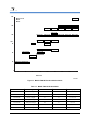
Vantis and JTAG-ISP
In 1994 the MACH445 device from Vantis was the first complex programmable logic device
introduced into the marketplace that had both in-system programmability and a fully compliant
implementation of the IEEE JTAG testability standard. Since then, a number of MACH devices have
been introduced which either have both JTAG testability and in-system programmability or have
only in-system programmability through a JTAG-compatible programming port. The MACH 4 and
MACH 5 families have both JTAG testability and in-system programmability with 3.3-V or 5-V options.
All MACH 1 and MACH 2 devices with “SP” in the part numbers are JTAG-compatible and have insystem programmability at no extra cost. Today, Vantis offers the largest selection of JTAG-ISP devices
in the industry. For the complete offering, please refer to the MACH JTAG-ISP Product Selection
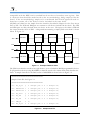
Guide (Figure 1-1) and the MACH JTAG-ISP Product Matrix (Table 1-1).
The MACH 1 & 2 SP devices, MACH 4 and MACH 5 families support the JTAG standard, which
means they can be included in any JTAG chain. With these devices, designers can design test
chains to work the way they want to, rather than having to conform to proprietary device
requirements. Non-JTAG CPLDs use proprietary programming techniques that require separate
setup and load processes and a separate set of test pins at a test station. With Vantis’ MACH
devices, users will realize major savings in both development time and manufacturing costs while
further increasing reliability.
1-3
Chapter 1
SpeedLocking tPD as fast as 7.5 ns or fCNT up to 133MHz when using up to 20 product terms
per output. Other features include mixed-voltage I/O safety, JTAG-ISP, asynchronous clocking
and programmable power-down modes.
V A N T I S
256
MACH 1 & 2 SP
MACH 4
MACH 5
M5(LV)-512
192
M5(LV)-192
M5(LV)-320 M5(LV)-384 M5(LV)-512
M5(LV)-320 M5(LV)-384 M5(LV)-512
M5(LV)-256 M5(LV)-320 M5(LV)-384 M5(LV)-512
M4(LV)-256
128
M5(LV)-128
M5(LV)-192
M5(LV)-256 M5(LV)-320 M5(LV)-384 M5(LV)-512
M5(LV)-128
M5(LV)-192
M5(LV)-256
I/Os
M4-96
96
M4(LV)-192
M5(LV)-128
M5(LV)-256
M4(LV)-128
MACH231SP
MACH131SP
64
M5(LV)-192
M4(LV)-96
MACH221SP
M4(LV)-32
M4(LV)-64
MACH111SP MACH211SP
32
0
32
64
96
128
192
256
320
384
512
Macrocells
21554A-1
Figure 1-1. MACH JTAG-ISP Product Selection Guide
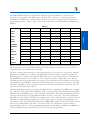
Table 1-1. MACH JTAG ISP Product Matrix
1-4
Device
Package
Macrocells
I/Os
tPD (ns)
MACH111SP
44PLCC/44TQFP
32
32
5/7.5/10/12/15
MACH131SP
100PQFP/100TQFP
64
64
5.5/7.5/10/12/15
MACH211SP
44PLCC/44TQFP
64
32
7.5/10/12/15
MACH221SP
100PQFP/100TQFP
96
48
7.5/10/12/15
MACH231SP
100PQFP/100TQFP
128
64
10/12/15
M4(LV)-32/32
44PLCC/44TQFP
32
32
7.5/10/12/15
M4(LV)-64/32
44PLCC/44TQFP
64
32
7.5/10/12/15
V A N T I S
Table 1-1 MACH JTAG ISP Product Matrix (Continued)
Package
Macrocells
I/Os
tPD (ns)
M4(LV)-96/48
100TQFP
96
48
7.5/10/12/15
M4-96/96
144 PQFP
96
96
15
M4(LV)-128/64
100PQFP/100TQFP
128
64
7.5/10/12/15
M4(LV)-192/96
144TQFP
192
96
10/12/15
M4(LV)-256/128
208PQFP
256
128
10/12/15
M5(LV)-128/68
100PQFP/100TQFP
128
68
7.5/10/12/15
M5(LV)-128/104
144PQFP
128
104
7.5/10/12/15
M5(LV)-128/120
160PQFP
128
120
7.5/10/12/15
M5(LV)-192/68
100PQFP/100TQFP
192
68
7.5/10/12/15
M5(LV)-192/104
144PQFP
192
104
7.5/10/12/15
M5(LV)-192/120
160PQFP
192
120
7.5/10/12/15
M5(LV)-192/160
208PQFP
192
160
7.5/10/12/15
M5(LV)-256/68
100PQFP/100TQFP
256
68
7.5/10/12/15
M5(LV)-256/104
144PQFP
256
104
7.5/10/12/15
M5(LV)-256/120
160PQFP
256
120
7.5/10/12/15
M5(LV)-256/160
208PQFP
256
160
7.5/10/12/15
M5(LV)-320/120
160PQFP
320
120
7.5/10/12/15
M5(LV)-320/160
208PQFP
320
160
7.5/10/12/15
M5(LV)-320/184
240PQFP
320
184
7.5/10/12/15
M5(LV)-320/192
256BGA
320
192
7.5/10/12/15
M5(LV)-384/120
160PQFP
384
120
7.5/10/12/15
M5(LV)-384/160
208PQFP
384
160
7.5/10/12/15
M5(LV)-384/184
240PQFP
384
184
7.5/10/12/15
M5(LV)-384/192
256BGA
384
192
7.5/10/12/15
M5(LV)-512/120
160PQFP
512
120
7.5/10/12/15
M5(LV)-512/160
208PQFP
512
160
7.5/10/12/15
M5(LV)-512/184
240PQFP
512
184
7.5/10/12/15
M5(LV)-512/192
256BGA
512
192
7.5/10/12/15
M5(LV)-512/256
352BGA
512
256
7.5/10/12/15
Chapter 1
Device
1-5
CHAPTER 2
2
Introduction to JTAG
History of JTAG
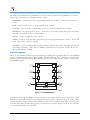
JTAG from the Top
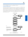
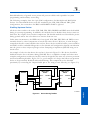
In its simplest form, JTAG can be implemented using a four-pin, dedicated test access port, a
synchronous state machine with 16 states, a group of data registers including a bypass register
and boundary scan cells (used to control the inputs and outputs of the device being tested). It
also needs an instruction register and instruction register decoder which is used to control the
data registers. Figure 2-1 shows a top-level diagram of a basic implementation of the IEEE 1149.1
standard.
TDI
TCK
TMS
Instruction Register
and
Instruction Register Decoder
TAP
Controller
TDO
Data Registers
and
Test Logic
System and Device Logic
21569A-1
Figure 2-1.
Publication# 21569
Amendment/0
Rev: A
Issue Date: September 1997
JTAG Block Diagram
2-1
Chapter 2
For years many companies have used proprietary test methodologies implemented with boundaryscan registers to reduce test complexity at the board and system level. In 1985 several European
companies formed a group with the purpose of standardizing a method for implementing and
performing boundary-scan testability. This group included representatives from board-test
companies, system design companies and semiconductor manufacturers. A year after this group
was formed, additional companies from both Asia and the United States joined it and continued
work on a standard to be voted on by the IEEE. The group is called Joint Test Action Group (JTAG).
In 1990 this standard was passed as standard IEEE 1149.1-1990, which is known as JTAG. This
standard included a definition for a Test Access Port (TAP), a group of both mandatory and
optional test registers, a control mechanism and timing for both the registers and TAP, and a set of
mandatory and optional test instructions. In 1993 corrections and additions were made to the
standard including a language that can be used to describe an implementation of JTAG in a given
device. This language is called the Boundary Scan Definition Language (BSDL) and is a subset of
VHDL (another IEEE standard). The Joint Test Action Group still meets on a regular basis and is
constantly working on improving the standard.
V A N T I S
There are four pins which make up the Test Access Port or TAP; TDI (Test Data Input), TMS (Test
Mode Select), TCK (Test ClocK) and TDO (Test Data Output). There is an additional pin defined
by the standard, TRST*, which can be used to asynchronously reset both the TAP controller and
the instruction register. All registers along with the TAP controller are clocked using the TCK pin.
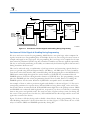
JTAG TAP Controller
The TAP Controller is a synchronous, finite state machine that controls both the TAP and the
various JTAG registers. It controls whether a device is in reset mode, where the core logic has full
control of the device, if it is receiving an instruction, receiving and/or transmitting data, or is in an
idle state. The state machine, as illustrated in Figure 2-2, is completely controlled by TMS and is
clocked by TCK. The value of TMS is located next to each transition in Figure 2-2.
1
TEST-LOGIC
RESET
0
0
RUN TEST/IDLE
1
1
SELECT-DR
SELECT-IR
0
1
0
1
CAPTURE-DR
CAPTURE-IR
0
0
SHIFT-DR
0
1
EXIT1-DR
1
1
EXIT1-IR
0
0
PAUSE-DR
0
PAUSE-IR
1
0
1
EXIT2-DR
0
EXIT2-IR
1
1
UPDATE-DR
1
0
SHIFT-IR
1
0
1
0
UPDATE-IR
1
0
21569A-2
Figure 2-2.
TAP Controller
JTAG Instructions
Where the TAP controller is the heart of any IEEE 1149.1 implementation, the instruction register and
instruction register decoder can be thought of as the brains. The instruction register stores information
concerning what test register or test circuitry is active. The construction of the instruction register is
such that for any instruction code selected, there is an associated register and/or test circuit which is
also selected. This is one of the requirements stated in the IEEE 1149.1 standard. Instructions can be
shifted into the instruction register only when the TAP controller is in the SHIFT-IR state and will
become active when the controller enters the UDPATE-IR state.
2-2
V A N T I S
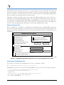
The MACH JTAG-ISP devices contain three different types of instructions. The first set of
instructions is required by the IEEE 1149.1 standard. The second set is optional instructions
included in the IEEE 1149.1 standard while the third set consists of proprietary instructions for
programming a device. Table 2-1 gives a list of the instructions used by the different MACH device
families.
Table 2-1.
Required
Optional
Proprietary
MACH 1 & 2 SP
MACH 4
MACH 5
X
X
X
X
EXTEST
X
X
X
SAMPLE
X
X
X
HIGHZ
X
X
X
X
IDCODE
X
X
X
X
USERCODE
X
Chapter 2
BYPASS
X
PGMMODE
X
X
X
X
ROW
X
X
X
X
COLUMN
X
X
X
X
PROGRAM
X
X
X
X
ERASE
X
X
X
X
VERIFY
X
X
X
X
SECURITY
X
X
X
X
Each of the above instructions has a unique, 6-bit code which is shifted into the instruction register.
The exception to this is the BYPASS instruction which will turn on whenever its own code is
selected or when an invalid code is selected.
The three required instructions have strict requirements as to how they are expected to operate,
defined in the IEEE 1149.1 standard. The BYPASS instruction enables a single bit register, the
BYPASS register, to shift data from TDI to TDO and leaves the part functioning in a normal mode.
The SAMPLE instruction is used either to take a snapshot of what is happening at the I/Os by
capturing pin data into the boundary scan register, or to load data into the boundary-scan register
in preparation for an EXTEST. It does this without affecting the functioning of the part. The third
instruction, EXTEST, is used to perform connectivity tests by controlling the inputs and I/Os of a
part with the boundary scan register.
The three optional instructions provided in the MACH devices are defined in the IEEE 1149.1 standard,
also. The first of these instructions, HIGHZ, is used to tri-state all I/Os while shifting data from TDI to
TDO through the BYPASS register. This instruction is included so that during programming, the I/Os
of devices not currently being programmed could be set into a “safe” state. The second instruction,
IDCODE, is used to shift out a 32-bit factory signature for a device. This signature is used by both test
equipment and programming equipment to verify a device they are testing or programming is the
correct device type. The third optional instruction, USERCODE, is unique to devices which have some
form of non-volatile memory on them. It is used to read out a 32-bit device signature which is
programmable by the user. The programming information for this field is included in the JEDEC file
and is programmed at the same time the rest of the device gets programmed.
2-3
V A N T I S
The final set of instructions is proprietary to Vantis and is used in the programming of a device.
Each of these instructions is explained briefly below.
PGMMODE - Used to turn on the programming mode by shifting a 5-bit password into the
device.
ROW - Used to select a row to be programmed or verified.
COLUMN - Used to shift in column data for the row to be programmed or verified.
PROGRAM - Used to program a device. To do this, a row must first be selected, and column
data must be loaded into the column register.
ERASE - Used to completely erase a device.
VERIFY - Used to verify that the correct data has been programmed into a device. To do this
a row and column must be selected.
SECURITY - Used to program the security bit which protects the device configuration data by
preventing read back. Only after an “ERASE” instruction has been done, can the device be
reprogrammed and verified.
JTAG Data Registers
There are two mandatory data registers defined by the IEEE 1149.1 standard. These are the BYPASS
register and the boundary-scan registers (BSR). The BYPASS register is a single-bit register which
is used to shift data from TDI to TDO without affecting any other circuitry. Figure 2-3 illustrates
the BYPASS register.
TDI
TDO
BYPASS
21569A-3
Figure 2-3.
BYPASS Register
A boundary-scan register (BSR) is used to capture or send data from the I/O or input pins. Each
boundary-scan cell for an input pin is composed of two registers. The first register is used to either
capture data from the pin or have data shifted into and out of it from the TAP. The second register
is used to drive data from the first register onto an input or I/O pin. Figure 2-4 shows the structure
of a typical boundary-scan cell (BSC).
2-4
V A N T I S
Input
0
To Next BSC
1
0
D
1
Q
Output
D
Q
BSC
TCK
From Previous BSC
UPDATE-DR
21569A-4
Boundary-Scan Cell
Every I/O cell has three boundary-scan registers attached to it. The first is for the input, the second
is for the output and the third is for the output enable. By looking at all three registers, test
software can tell exactly what is happening at that I/O pin. If the output enable is a “1”, then the
I/O pin will be whatever the value of the output cell is. If the output enable is a “0”, the I/O pin
is configured as an input with the value of the data in the input BSC. An input or clock pin would
have only a single BSC and would not have the output tied to anything as it is used for observation
only. Figure 2-5 shows the BSC configurations for both the input pin and the I/O pin.
BSC for Inputs
BSC for I/Os
TO NEXT
CELL
BSC
To Next
Cell
System
Logic
Macrocell
BSC
BSC
BSC
From Last Cell
21569A-5
Figure 2-5.
BSC Configurations
For a device to be considered IEEE 1149.1 compliant, it must have the TAP, TAP controller, BYPASS,
SAMPLE and EXTEST instructions and a boundary-register. A device which has only the TAP and TAP
controller may be compatible with the IEEE 1149.1 standard and may work in a scan chain, but it will
not be considered compliant. Any device which does not have a boundary-scan cell cannot be tested
using the TAP because there is no means of controlling and accessing the I/O and input pins other than
a direct connection. All of the MACH 4 and MACH 5 devices are compliant with the IEEE 1149.1
standard while the MACH 1 & 2 SP devices are considered compatible.
2-5
Chapter 2
Figure 2-4.
3
CHAPTER 3
Introduction to In-System Programming (ISP)
Introduction
In-system programming (ISP) was developed to make it easier to use programmable logic devices
packaged in fine pitch packaging, such as the Plastic Quad Flat Pack (PQFP) or Thin Quad Flat
Pack (TQFP) packages. A typical manufacturing flow that does not use ISP requires additional
handling steps which increases the probability of damaging delicate leads and decreases the
manufacturing yield. Over the past several years, the use of ISP has increased greatly as has the
number of devices that offer the ability to be programmed in-system. In fact, ISP is quickly
becoming a requirement for any new devices introduced.
There are very few limitations placed on what kind of system can be used to execute an ISP algorithm.
Today, most programmable logic companies offer programming solutions which range from
programming a single device through a simple cable, attached to a computer, to programming several
devices as part of a board test program. Also offered is the ability to program devices using a
microprocessor on the same board as the devices being programmed. This is referred to as embedded
programming and can give users the ability to update the programming in a device in the field.
To successfully program, in-system, there are a few simple requirements which must first be met.
The first of these requirements is that the devices on the board need to be correctly connected
into a JTAG scan chain. This scan chain can be used for either programming or testing the board.
To program using the Vantis MACHPRO software, a description of the JTAG scan chain needs to
be developed. This description is called a chain file which contains information about all of the
devices in the chain including device type, instruction register length (six bits for all MACH
JTAG-ISP devices), the JEDEC file being programmed into the device with associated output file,
and any optional features needed during programming such as tri-stating the I/Os, programming
the security bits, etc. Additional information about the chain file and its construction is given in
the MACHPRO User Manual in the Appendix B of this manual.
Another requirement for successful programming is thoughtful board design. The signals used in a
JTAG scan chain (TCK, TMS, TDI and TDO) will rarely run as fast as the remainder of the signals on
the board but still require correct board layout methodologies such as buffering for large chains,
termination resistors, etc. These board layout methodologies are described in Chapter 4 of this manual.
After all of these requirements have been met, it should be relatively straightforward to program
any number of devices on a board. This programming can be done using a PC with a cable
attached to the board or a board test system. MACHPRO can easily be used to program in any of
these environments.
JTAG Scan Chains
A JTAG scan chain can contain one or more IEEE 1149.1 compliant, programmable and
non-programmable devices. It can also include any programmable devices that are
Publication# 21568
Amendment/0
Rev: A
Issue Date: September 1997
3-1
Chapter 3
Basics of Programming
V A N T I S
compatible with the IEEE 1149.1 standard but do not have a boundary-scan register. This
is a decision that should be made based on the test methodology being employed for the
board. If the test methodology employed is a traditional bed-of-nails approach used on
board test systems, all of the devices can be included in the same chain.
All JTAG scan chains use the simple four-wire interface described in Chapter 2 as the Test Access
Port or TAP. The TCK and TMS pins are common to all devices included in the chain. The TDI
and TDO pins are daisy-chained from one device to the next. The input to the chain is TDI and
the output from the chain is TDO. A diagram demonstrating a simple JTAG scan chain is shown
below in Figure 3-1.
TDI
M4-64/32
MACH211SP
MACH131SP
M5-512/160
M4-64/32
AMD-K6
M4-128/64
M4-256/128
TCK
TMS
TDO
21568A-1
Figure 3-1.
Example JTAG Scan Chain
The JTAG scan chain shown above has eight devices, seven of which are MACH programmable devices.
To program these devices using MACHPRO, a chain file needs to be written which fully describes the
chain. A sample chain file for the DOS version of MACHPRO is shown below in Figure 3-2.
;*******************************************************
;Sample Chain File for Figure 3-1
;*******************************************************
‘U1’
M4_64_32
p
6
design1.jed /-o Z -f design1.out;
‘U2’
MACH211SP
v
6
design2.jed /-o Z -f design2.out;
‘U3’
MACH131SP
n
6
design3.jed /-o Z -f design3.out;
‘U4’
M5_512C7
p
6
design4.jed /-o Z -f design4.out;
‘U5’
M4_256
p
6
design5.jed /-o Z -f design4.out;
‘U6’
M4_128
m
6
design6.jed /-o Z -f design5.out;
‘U7’
AMD_K6
n
5;
‘U8’
M4_64_32
n
6
design7.jed /-o Z -f design7.out;
Figure 3-2.
3-2
Sample Chain File
V A N T I S
Additional detailed information on how to generate a chain file for both the Windows and DOS
versions of MACHPRO is presented in the MACHPRO User Manual.
Programming Algorithm Basics
Programming a CPLD is similar to programming any piece of memory such as an EPROM or FLASH
memory. The device can be thought of as an array that is programmed one row at a time. The
programming information is provided to the software in the form of a standard JEDEC file that is
then converted into the row and column data. Before an EEPROM device can be programmed, it
first has to be erased. After the device has been erased, the programming data can be loaded and
the device programmed. After the device has been programmed, it will be verified by reading out
the data in the device and comparing it against the original. Figure 3-3 below shows the basic
programming flow for the device. It does not include JEDEC file data conversion as it assumes
that has already been done.
START
Preload or Save
Yes
Preload/Save I/O using
SAMPLE/PRELOAD
I/O states?
Chapter 3
No
Enter Programming Mode
Erase Device
Program Device
Verify Device
Notes:
1. Although it is not necessary, a
reset should always be performed
before and after programming a
device
2. If the device will not be programmed
in-circuit (i.e. via a cable or using an
embedded processor) then it is not
necessary to Preload or Save the
I/O states
Secure Device?
Yes
Program Security
Fuses
No
Reset Device
END
21568A-2
Figure 3-3.
Programming Routine Flow
3-3
V A N T I S
This programming flow will be the same regardless of the programming hardware used. The
primary difference between programming on different hardware platforms is the type of data
format used.
Programming Time
The time it takes to program a device can often be a determining factor of where in the
manufacturing process a device, or a group of devices, is programmed. A board test system costing
hundreds of thousands of dollars to purchase and costing as much as one dollar per minute to run
can be an expensive alternative for programming if programming times are too long. In many
instances it will be more cost effective to have a couple of PCs and program the devices using
these less expensive systems.
The time it takes to completely program a device is based on the time it takes to first erase the
device, then program each row in the device, and then finally to verify the device. The erase time
for all MACH devices is the same and is specified at 100 milliseconds. In any given MACH device,
there are between 76 and 82 rows of data to be programmed. A single row is programmed in 50
milliseconds. The verify process is the quickest of the required steps in the programming sequence
and should take no more than 0.3 seconds to shift the verify data out on any given device. All
totaled, the theoretical minimum time needed to program a single device on a board is on the order
of 4.5 seconds.
One of the options offered by MACHPRO is the ability to do parallel programming. This type of
programming allows multiple devices to be programmed at the same time, thereby reducing the
overall number of programming wait states required. As a result, the additional time needed to
program additional devices is only that time needed to shift in the additional programming data
and to verify the additional devices. The time required to program a single M4-128/64 device is
about 4.5 seconds. On a board test system, where devices can be programmed in almost the
minimum time, it takes only 9 seconds to program ten M4-128/64 devices on the same board.
The minimal programming times will only be seen on board test systems because they are included
as a part of the test program and are running at the fastest speed possible. Additionally, there is
no translation needed to or from JEDEC formatted data as this has already been done by the
MACHPRO software.
Programming on a PC
Programming on a PC is done through a simple cable attached to the parallel port. The design for
this cable is shown in the Appendix. Additional information concerning programming on a PC
through MACHPRO is shown in the MACHPRO User Manual.
Programming on a Board Test System
Programming on a board test system is made possible by using MACHPRO to generate the
necessary programming files needed for the different platforms. The platforms supported by
MACHPRO include Teradyne, GenRad and Hewlett Packard board test systems. Additional
information on programming on any of these systems is shown in Chapter 5 of this manual.
3-4
V A N T I S
Programming on JTAG Test Systems
JTAG test systems differ from traditional board test systems in their basic test methodology. These
systems use only the four wire JTAG TAP to perform any interconnect and functional tests. A simple
language has been developed to interface with the TAP and is used by most major JTAG test system
vendors. This language is known as the Serial Vector Format and is supported by MACHPRO.
Information on generating an SVF programming file is given in the MACHPRO User Manual.
Chapter 3
3-5
4
CHAPTER 4
MACH In-System Programming–
Design & Usage Guidelines
Introduction
In-system programming has often been billed as a direct replacement for configuring a device
through a programmer. The thought that devices can just be placed on a board, hooked up to a
PC through a cable and programmed is an attractive alternative for many of today’s package
options such as the Thin Quad Flat Pack (TQFP) or the Ball Grid Array (BGA). Whenever devices
are put on a board, care must be taken in the design of that board in terms of loading of the clock
lines, buffering, and termination of signals. This is just as true for the ISP signals as it is for the
data-path or control signals generated or used by a device. For this reason, it is necessary to follow
some guidelines when designing in-system programmability into a board.
An ideal setup for ISP would include buffers at both the parallel port connection of a short cable
and on the board to be configured, termination of all lines which are run in parallel such as TMS
and TCK, and Schmitt trigger inputs on all devices which are a part of the programming chain.
This is not always practical or feasible, however, because there may be only a few devices in the
chain, a cable with buffers might not be available, or non-MACH devices in the chain which may
not use Schmitt trigger inputs. Because of such limitations, the following recommendations are
made as guidelines which should make for a smoother ISP experience.
Connections
The MACH devices typically come in two ISP configurations. The first configuration has the four standard
JTAG pins, TCK, TMS, TDI and TDO, plus an asynchronous reset pin, TRST* and a program enable pin,
ENABLE*. This configuration is found on the M4-128/64 and M4-256/128 devices. The second
configuration uses only the four standard JTAG pins and is found on all other MACH JTAG-ISP devices.
◆ For new designs, the TRST* pin should be permanently tied to VCC and the ENABLE* pin should
be tied to GND.
Making the connections recommended above will simplify the layout of a board and will eliminate
the need for additional buffers for those signals.
After programming and testing have been completed, the question often arises, “what should be
done with the ISP port signals?” One of the requirements in the IEEE1149.1 standard for the JTAG
port is that both the TMS pin and the TDI pin have internal pull-up resistors. By ensuring that
there is a “1” on the TMS pin, inadvertent clocking of TCK will not cause the JTAG state machine
to leave its reset state. The MACH devices also have a pull-up resistor on the TCK pin.
◆ After programming, while it is not required, a 4.7K pull-up resistor can be used on the TCK and TMS
signals on a board. As the number of devices connected to the TCK/TMS signals increases, the need
for pull-up resistors decreases as more internal pull-up resistors are affecting those signals.
Publication# 21570
Amendment/0
Rev: A
Issue Date: September 1997
4-1
Chapter 4
In a programming environment, it is necessary only to connect the four standard JTAG pins
regardless of the configuration. With the six-pin configuration, while MACHPRO supports the use
of the TRST* pin and ENABLE* pin, it is not a requirement.
V A N T I S
Buffering
As stated earlier, the ideal scheme for buffering includes buffers at both ends of the cable, and
buffers for each group of four or five devices in the programming chain. This case does not cover
all situations, however. There could be a design with only two devices in the chain; in that case,
the question “is a buffer needed?” arises. The recommendation for buffering is as follows:
◆ Buffering is needed for the TCK, TMS, and TRST* lines. It should also be used for the TDI signal
into the board and the TDO signal out of the board.
The TCK, TMS, TRST* and ENABLE* signals (TRST* and ENABLE* are only on M4-128/64 and
M4-256/128 devices) are run in parallel to all JTAG and JTAG-ISP devices on a board. Because
of this, these signals will tend to present a larger load to the source driving them. In many
cases, this is the parallel port of a PC which may or may not have a strong drive capability,
based on the manufacturer of the computer. For this reason, we recommend using a buffered
cable which is no longer than six feet, shorter if the programming setup allows for it. The
transmission line effects of both the cable and the traces on the board are the cause for the
recommendation of additional buffering on the board itself. The TDI and TDO signals of each
device are daisy-chained where the TDO of one device will feed the TDI of the next.
◆ If there are fewer than five devices in a programming chain, buffers are not required, but are
recommended. If there are five or more devices, buffering is recommended, as well as a
separate buffer for each group of five to eight devices.
◆ When using a buffer, trace lengths should be balanced to minimize signal skew.
The more devices connected to a given signal, the greater the loading on that signal. For that
reason, it is necessary to buffer heavily loaded signals and to split the loading of a given signal so
that there is a smaller load. This load should also be balanced, both in terms of the number of
devices driven by that signal, and the lengths of the traces to each device, so that signal skew does
not become an issue.
◆ If non-MACH devices are included in the chain which do not use Schmitt trigger inputs, it is
recommended that Schmitt trigger buffers be used and that the buffer be placed closest to the
devices which require those inputs.
All MACH JTAG-ISP devices have Schmitt trigger inputs for pins in their programming port. This
is done because the signals coming from the parallel port of a computer 6 feet away are often very
noisy and the Schmitt triggers tend to make the device more noise-immune. Many devices which
incorporate a JTAG interface and which may be placed into the programming chain will not have
Schmitt trigger inputs and, as a result, will be more susceptible to noise problems. In general,
these devices are designed for use in either a board test environment or other environment which
can be significantly cleaner than being driven by the parallel port of a computer.
◆ A buffered cable should be used when available. The length of this cable should be no more
than 6 feet and should be minimized.
Vantis recommends a design for a buffered cable shown in Appendix A. This design will work for
most situations. The cable should be made as short as possible to reduce transmission line effects
and should be no longer than 6 feet in length. There are several buffers which are suitable for use
in the programming chain. These include 74LS244, 74LS367 and 74HC244. When selecting a buffer,
one parameter to watch for is the output edge rates. If they are too fast, reflections can become a
4-2
V A N T I S
real concern. Additionally, all MACH devices have inputs which are 5-V compatible, so on a board
which uses only a 5-V supply or on a board with mixed 3.3-V and 5-V supplies, a 5-V buffer can be
used. On a board which uses only a 3.3-V supply, a 3.3-V buffer can be used.
The correct use of buffers, both in the cable and on the board, can go a long way in either solving
existing programming problems or preventing them. It is not the only consideration, however.
Termination of Signals
In any high speed board or system design, termination of signals is often required to ensure
reliable operation. The same is true in an ISP environment. Termination and correct board layout
techniques can go a long way to developing a reliable programming setup. Some of the effects
of not terminating a signal can be negative overshooting, where a signal will glitch to a negative
voltage for a very short period of time (< 2 ns), or double clocking, where a clock signal may have
a negative glitch on its rising edge. Both situations can be devastating in an ISP environment. To
prevent such possibilities, the following steps should be taken.
◆ Avoid using buffers with extremely fast edge rates such as the 74F244.
◆ Terminate the TCK signal either using a balanced termination network on the main trunk of the
signal or by using 68 ohm resistors in series with each pin the TCK signal is connected to.
Decoupling Capacitors
Decoupling capacitors are a must for any board using high pin count devices. When they are not
used, there can be problems caused by the large current usage required when I/Os are changing
states. The usual recommendation for decoupling capacitors is a 0.01 or 0.1 µF ceramic capacitor
on each side of a device along with a single 10 µF tantalum capacitor for the entire device. For
many of the lower pin count devices, this may be overkill and the number of capacitors can
probably be reduced to two 0.01 µF ceramics along with the single 10 µF tantalum.
When Buffers Are Not Used
If there are noise problems, they can often be cleaned up using a simple RC filter on both the TCK
and TMS signals and on the TDI signal into the first device. Additionally, the ISP devices may not
always have enough drive capability on their TDO pins to either pull-up or pull-down a signal, six
feet away, at the parallel port. In this situation the following measure can be taken.
◆ A 4.7K pull-up or pull-down resistor may be necessary on the TDO signal of the last device in
the programming chain to reliably switch the signal into the parallel port. This should only be
necessary if buffers are not being included as a part of the board design.
Debugging in the ISP Environment
If all of the above guidelines are followed concerning board layout and design, the programming
should go smoothly and reliably. There may, however, be other problems which could be the
result of improper settings in the MACHPRO software, a computer which is too fast for the
programming chain, etc.
4-3
Chapter 4
While buffers are recommended for all designs, they may not always be practical in a smaller
design where there are only one or two devices in the programming chain. In this situation, there
are still precautions which can be taken to minimize problems.
V A N T I S
There are two situations where problems can occur. The first is when MACHPRO is checking the
structure of the programming chain by reading the device factory signature of all MACH JTAG-ISP
devices in the chain and checking for a single bit from all other devices. If an error occurs at this
time, it will most often read “ID does not match part ID.” If this happens, do the following:
◆ If the errors returned are either all “1” or all “0”, the following could be wrong:
— The programming/JTAG connections are incorrect and should be checked.
— If the 6-pin configuration with the TRST* pin is used and connected, the strobing done by the
parallel port needs to be turned off. This can be done in the Windows version of MACHPRO
by deselecting the “Any key attached to parallel port” option under the Project|Options menu.
Any software keys connected to the parallel port must then be removed. In the DOS version
of MACHPRO, the -j 0 option must be used.
— The programming chain has been incorrectly specified. Check both the order of the devices
in the chain and the number of instruction register bits in each of the non-MACH devices.
◆ If the errors returned are a combination of “1” and “0” and they vary, the TCK and TMS lines
may not be either sufficiently terminated or buffered. Please refer to the guidelines above.
The other time an error could appear is during the bit verify stage of the programming cycle. If
this happens, and the IDCODE correctly reads out, the problem is most likely that the computer
system being used is too fast and data on TDO of the device being verified did not have enough
time to settle before being shifted through the rest of the programming chain. This can sometimes
be seen on Pentium systems running at 133MHz or faster. If this happens, the following remedy
can be used.
◆ MACHPRO can specify a longer settling time in both the DOS and Windows versions of the
software. In the Windows version this is done by deselecting the “Any key attached to parallel
port” option under the Project|Options menu and by specifying a new delay value in the
Project|Advanced Options window. The default value is 50 and should be incremented by 50
or 100 until the system works. If errors continue with a delay of 1000 or more, please check
the connections and make sure the design guidelines above have been followed. In the DOS
version of MACHPRO, the delay is set using the -j X -w options where X is the value for the
delay.
I/O States During Programming
During a programming cycle, all MACH JTAG-ISP devices default to having their I/Os tri-stated. In
most situations, this probably will be acceptable and will not cause any problems. There are
situations which arise where it may cause some contention. Through the boundary scan cells of
the MACH 4 and MACH 5 devices, MACHPRO offers the ability to set all I/O pins to a state of “1”,
“0”, HIGHZ or don’t care, and to set the state of each I/O pin individually. Refer to the MACHPRO
User Manual for instructions on how to use this feature.
Conclusion
The design guidelines and debug techniques presented here should lead to a reliable JTAG-ISP
design and programming flow. JTAG-ISP offers many advantages over traditional programming
techniques, but additional considerations must be taken into account when implementing it, such
as proper buffering and termination. This will ensure an effective and productive ISP experience.
4-4
CHAPTER 5
5
Programming MACH JTAG-ISP Devices on
Automated Test Equipment
Introduction
The MACH JTAG-ISP devices are in-system programmable through the test access port pins by a PC
or Automated Test Equipment (ATE). This offers advantages in the design, manufacturing and
maintenance phases of a product’s life cycle. Designers can develop systems with reconfigurable
MACH JTAG-ISP devices connected in series in a boundary scan chain with other JTAG-compliant
devices for testability (Figure 5-1).
JTAG
Interface
Connector
M5-512
Connect to PC
parallel port or
board tester test
pins
TDI
M4-256
TDI TDO
TDI TDO
TMS
TMS
TCK
TCK
TMS
TCK
TDO
M4-128
AMD K6
74ABT502
TDO TDI
TDO TDI
TDO
TDI
TMS
TMS
TMS
TCK
TCK
TCK
21146B-1
Figure 5-1. Board with 5 JTAG devices connected in a serial JTAG chain.
TDI and TDO are connected in series while TMS and TCK are in parallel
MACHPRO, the Vantis-developed PC-based software tool, is ideal for configuring the MACH devices
on the board through the same IEEE 1149.1 test interface used for board testing via a PC parallel port
programming cable. Any subsequent logic changes in the MACH devices can be performed quickly
on the board connecting to a PC development station without having to remove or reinsert the parts.
Designers can therefore attempt more design iterations to debug and improve product performance.
Publication# 21146
Amendment/0
Rev: B
Issue Date: September 1997
5-1
Chapter 5
JTAG-ISP: A Long-Term, Cost-Effective Solution
V A N T I S
Once the design has been finalized and is ready for manufacturing, MACHPRO can generate an
output file for the target ATE or board tester. Now, manufacturing engineers can incorporate the
programming of the MACH devices into the board manufacturing flow. Programming MACH
devices on the tester during manufacturing offers many advantages:
◆ Programming and pattern verification is fast and is determined by the tester clock rate and the
programming time requirements of the devices
◆ Programming on the ATE removes the cost of maintaining and upgrading a separate
programming station
◆ Component damage is minimized by reducing handling of the devices with fine-pitch leads
The MACH JTAG-ISP devices can be treated as generic devices that can be loaded directly onto a
printed-circuit board and configured with the required patterns during the manufacturing and test
flow. Programming on the tester eliminates the possibility of a device with the wrong pattern being
placed on the board. Since MACH devices have fast programming times, combining programming
and board test on the same ATE station will have minimal impact on the manufacturing beat rate.
Once the product has been released to the end-user, logic updates can be performed easily in the
field by a technical support person with the new programming patterns, a notebook PC and a
programming cable. Designers can also design the board such that MACH devices in the JTAG
chain can be configurable through a microcontroller. Updated software and new programming
patterns can be delivered via disk or modem to customers with these microcontroller- or
microprocessor-based systems, and they can perform the updates themselves.
Programming on Board Testers
MACHPRO has options for generating vector files for programming MACH devices on board testers
from the major ATE vendors: GenRad, HP and Teradyne. Since the MACH 4 and MACH 5 devices
are IEEE 1149.1-compliant, MACHPRO can generate programming and pattern verification vectors
for these devices that are in a serial chain with other non-MACH JTAG-compliant devices. The
position of the MACH devices in the serial chain and the operations to be performed on them are
described in an ASCII file called a JTAG chain description file. (Refer to the MACHPRO User Guide
for information on creating and processing a JTAG chain description file.) Any MACH parts that do
not need to be reconfigured and all non-MACH devices are put into bypass mode by MACHPRO.
By using the JTAG interface for MACH device programming, manufacturing engineers do not need
any special programming software because the programming vector files can be treated as regular
test programs. Manufacturing engineers can therefore process the MACHPRO-generated files with
existing JTAG or boundary scan test software supplied by the ATE vendor and convert it to the
native tester language format before downloading it to the tester.
Printed Circuit Board Layout Considerations for Boundary Scan Chains
Ground access points (vias, component leads etc.) should be numerous and distributed evenly
across the entire PCB. The even distribution of ground access points across the surface of the PCB
helps to reduce the wire length on the ground probes and reduces the effects of ground bounce.
Large boundary scan chains must have a substantial number of ground access points distributed
across the PCB. This will enable the fixture design software to generate short ground wires
throughout the fixture. The number and distribution of ground access points will be the single
most important factor in determining the signal integrity of the in-circuit test fixture. Poor and
5-2
V A N T I S
limited distribution of ground access points will prevent reliable and repeatable in-system
programming and boundary scan testing.
The following examples show the 6-pin JTAG configurations for M4-128/64 and M4-256/128
devices. For other MACH devices with the standard 4-pin (TCK, TMS, TDI and TDO) JTAG
configurations, the connections for TRST* and ENABLE* should be ignored.
Disabling Upstream Devices
All devices that can drive the nodes TCK, TMS, TDI, TDO, ENABLE* and TRST* must be disabled
during in-system programming. In addition, the methods used to disable these devices must not
back drive the outputs of any another components. The disable methods used should also persist
during periods where the tester drivers are inactive between tests.
Under most circumstances, the IEEE 1149.1 bus signals TCK, TMS, TDI, TDO and TRST* are not
normally driven by other components or bused with other devices. However, in some designs,
components do take control and drive the test bus. These devices could be buffers, scan controllers
and ASICs used for embedded diagnostics or for dynamic self-configuration. Special consideration
must be given to these unique topologies when attempting to implement JTAG-ISP using an incircuit tester.
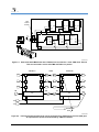
An example of a device that shares the test bus is shown in Figure 5-2. This device should be
disabled from the bus at all times during JTAG-ISP. This is a simplistic example and other more
complex configurations could exist, but they must be designed in the same way to insure persistent
and non-backdriving disables. Figure 5-2 is a good example of a design that allows an upstream
device to be persistently disabled without backdriving. This component can be disabled
persistently by connecting the Output Enable pin to VCC using a tester GP relay (see Figure 5-3).
IEEE-1149.1
MACH
74HC244
TRST*
TDI
OE
ENABLE*
TDO
TMS
TCK
IEEE-1149.1
MACH
TRST*
TDI
ENABLE*
TDO
TMS
TCK
21146B-2
Chapter 5
Figure 5-2.
Device Sharing Test Bus
5-3
V A N T I S
VCC
GP Relays
TRST*
VCC
Pull Up
Resistors
on TCK
and TMS
TDI
OE
GP
Relay
IEEE-1149.1
MACH
IEEE-1149.1
MACH
74HC244
ENABLE*
TDO
TMS
TCK
TRST*
ENABLE*
TDI
TDO
TMS
TCK
21146B-3
Figure 5-3.
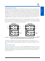
Persistence of Critical Signals and Disabling During Programming
Persistence of Critical Signals & Disabling During Programming
File sizes and vector counts for programming MACH devices are quite large when compared to
regular in-circuit tests. Programming files for multiple devices are far too large for most testers to
compile and apply in one single pass. If a programming file is too large to be compiled on its own
then it must be partitioned (broken up) into a number of smaller tests that are applied sequentially.
The key to successful partitioning is the ability to continuously hold critical signals in known states
during transitions between tests.
This can be achieved using a combination of pull up resistors and connecting signals directly to
power or ground using General Purpose Relays (GP Relays). All TRST* pins on every boundary
scan device in the chain must be fully controlled along with all program pins on the MACH devices.
TRST* must remain high throughout the entire duration of JTAG-ISP. We recommend that all
ENABLE* pins are fixed low throughout the duration of JTAG-ISP also. The programming vectors
pulse the ENABLE* pin low when programming data has been loaded. However, holding the
ENABLE* pin low for the entire duration of JTAG-ISP is acceptable and is recommended.
An example of how to achieve persistent signals and disables is shown in Figure 5-3. The test is
strategically partitioned at a point where TCK and TMS are being driven high. At the end of the
first test the drivers are turned off and TCK and TMS remain high due to the pull up resistors. TRST*
and ENABLE* are continually held high and low, respectively, by the use of GP relays connecting
them to the power and ground nodes. The next test in the sequence always starts out driving the
last vector of the previous test. In this case, TCK and TMS will be driven high and the tester will
again take control of the device.
Figure 5-3 shows a GP relay being used to disable a bused device during programming. This is an
ideal disabling situation for a device that shares the test bus. Figure 5-3 also shows the use of GP
relays to hold the TRST* and ENABLE* persistently during ISP.
5-4
V A N T I S
Figure 5-4 shows an optimum scan chain design for JTAG-ISP. No other devices can drive the test
bus except the tester. Pull up and pull down loads are designed onto the PCB (not wired into the
fixture which adds additional wires on critical nodes). Only two devices are shown in Figure 5-4.
However, any number of IEEE-1149.1 devices could be bused together, occupying any position in
the scan chain. If other devices in the chain have a TRST* pin or “Compliance” pins (pins that must
be asserted to place them into boundary scan mode) then these signals must be controlled
persistently using GP relays or pull up/down resistors.
VCC
VCC
GP Relay
IEEE-1149.1
MACH
IEEE-1149.1
MACH
TRST*
TDI
ENABLE*
TDO
TMS
TCK
TRST*
TDI
GP Relay
ENABLE*
TDO
TMS
TCK
21146B-4
Figure 5-4.
Optimum Scan Chain Design for JTAG-ISP
Test Fixture Design Considerations For Boundary Scan Chains
Once the PCB has been designed and routed optimally for signal integrity, good ground access
and distribution in the test fixture design must be considered. There are a number of things a test
developer can do to reduce noise and increase signal integrity in the test fixture. The most
important factor will be wire lengths. Long wires introduce noise and reduce signal quality. Nodes
such as TCK and TMS must be marked “CRITICAL” in the HP3070 board test files so that during
fixture design the shortest possible wires are assigned. For other ATE equipment, similar
instructions or precautions must be followed to insure that TCK and TMS nodes have short wires.
Board placement can have an effect on signal integrity. When designing the fixture carefully place
the board over the tester resources, paying close attention to the points where TCK, and TMS nets
5-5
Chapter 5
Twisted pair wiring can also be specified for critical nodes. Twisted pair wiring can be selected for
these nodes using the HP3070 board consultant program. Twisted pair wiring in combination with
a ground plane is strongly recommended for very large boundary scan chains and multiple part
programming. All of the tester grounds should be wired to the plane with short low impedance
wires or ground rakes. There must be an adequate number of ground resources assigned in the
fixture. To increase the number of grounds specify a higher power supply current than required
to power the board. This will force the fixture design software to assign more ground resources.
If good PCB design practices are followed and ground access points on the board are numerous
and distributed adequately across the board then optimal short wire ground interfaces will exist.
V A N T I S
will be probed. Place the board so they are very near digital resources if possible. Also place the
board so that only a minimum amount of ground resources are blocked by probes. In particular,
pay close attention to the ground resources on the cards that drive the TCK, TMS and TDI nodes.
Try not to block any ground resources on these cards.
Obtaining a reliable and solid probe contact with TCK, TMS and TDI nodes is also crucial for
reducing noise and maintaining signal quality. Try to design the PCB with pad sizes greater than
35 mil at least for TCK, TMS, TDI, TDO, TRST* and ENABLE* access points. Space the points at
least 100 mil to 75 mil from other points so that 100 mil or 75 mil probes can be used. High force
(10 OZ.) and steel-tipped probes will help to obtain solid reliable probe contact.
Generating Vector Files
There are Windows 3.1, Windows 95, Windows NT and DOS versions of MACHPRO. To generate
the vector files in the Windows versions, click on the desired output format options (Figure 5-5).
There are equivalent command line options for generating ATE vector files in the DOS version of
MACHPRO.
MACHPRO Processing Options
Process all parts even if errors occur
Parallel Port (Hardware) keys
Reinitialize part on error
Any key attached to parallel port
Use compressed file format
Prompt for correct programming cable
if any key is
Compress JEDEC files
No prompt before overwriting result files
OK
Use parallel programming mode
ATE output formats
GenRad vector format
HP PCF format
Teradyne vector format
Cancel
Max Number of Vectors per File (Teradyne only)
200000
ATE Vector Output Filename
Serial vector format
Get Filename
SVF Vectors for Programming and Pattern Verification
SVF Vectors for Programming Only
21146B-5
Figure 5-5.
MACHPRO for Windows output option menu for specifying ATE vector formats
Generating a GenRad Vector File
To generate a vector file for a GenRad tester, use the “-4 filename” option.
Ex: C:\MPRO_DSG> machpro -I project -4 board1.vct
MACHPRO will generate a vector file called BOARD1.VCT with vectors in the following format:
! File [board1.vct] created Wed May 22 18:09:29 1996
! for GenRad preprocessor generated by
! MACHPRO(tm)
! Version 1.40h (c) 1994-1996 Advanced Micro Devices, Inc.
! Pin order: TCK,TMS,TDI,TRST,ENABLE,TDO
+unit Program_AMD_MACHS
5-6
V A N T I S
00011X
00011X
C1011X
C1011X
+begin id 1 register
C1011H
C1011L
+end id 1
C1011X
+wait 50m
C1111X
C0111X
+verify begin id 1
C1011X
C0011X
...
C1111H
+end verify id 1
...
C0011X
00011X
+end unit
Comments are preceded by a ‘!’ and continue to the end of the line. Lines which require special
processing are marked by a ‘+’. For example: The lines “+begin id 1 register” and “end id 1” are
used to bracket vectors for testing the device ID code for the first JTAG device in the chain. If you
have more than one MACH JTAG-ISP device being programmed in the chain, then you will have
similar sets of vector statements for each device with the number being the position of the device
in the chain.
Similarly, the statements “+verify begin id 1” and “+end verify id 1” are used to verify if JTAG
device number 1 was configured correctly. There are no special statements to mark which parts
are being programmed, but programming is performed by shifting in data and then waiting for a
predetermined amount of time. This is accomplished for the MACH devices by the line “+wait
50m” which means wait in this state for 50 ms.
Each line of the form XXXXXX (e.g., 00011H) specifies the state of each JTAG pin listed in the "Pin
order" statement. In the preceding example, 00011X means drive TCK, TMS, and TDI low, drive
TRST and ENABLE high, and test if the TDO pin is high. The tester drives the pins low or high if
0 or 1, respectively, is specified, and compares the state of the TDO pin at this time against H or
L as indicated. If it is X, then the tester does not need to test the TDO pin. A C will be compiled
into a clock pulse. The clock pulse will be issued only after the other inputs (i.e. TMS, TDI, TRST,
and ENABLE) have been set up.
GenRad’s test generator program is then run on the .DTS file to convert the model into a “.TPG” (test
program) compatible format. The .TPG file is then processed further and converted into a binary file
with the “.OBC” file extension. The .OBC file can now be downloaded and run on the tester.
5-7
Chapter 5
This vector file is processed by a GenRad-supplied program called AMD2GR.PRL to produce a
“.DTS” file which is a GenRad intermediate file format. The .DTS file is a test program written as
a model that can be stored in a library on the GenRad test system.
V A N T I S
GenRad offers a hardware option for their testers called Deep Serial Memory which eliminates the
overhead in loading test vectors. This reduces total programming and pattern verification time and
results in better tester throughput. Contact your local GenRad Applications Engineer for more details.
Programming on Teradyne Testers
There are two ways to program the MACH devices on the Z18XX series testers: through the Vector
Processor (VP) or the Digital Function Processor (DFP). The VP takes MACHPRO-generated
programming vectors and applies them to the JTAG interface while the DFP programs a MACH
device by processing the programming information specified in a JEDEC map.
The Teradyne Vector Processor
Use the MACHPRO command line with the “-3 filename maxvect” option to generate the vectors
for the VP:
Ex: C:\> machpro -I design3.chn -z 3 -3 teradyne.vct 150000
The maxvect option is used to specify the maximum number of vectors in a vector file. If this
number is exceeded, then MACHPRO automatically creates a new file or files to handle the
overflow. The files will have the names 0 0 0 0 0 0 0n.AMD where n ranges from 1 to the
maximum number of files required.
Upon completion of vector generation, MACHPRO will display a message indicating the total
number of vectors generated and the number of new files created:
C:\JTAG> machpro -i design3.chn -z 3 -3 teradyne.vct 150000
MACHPRO(tm) Version 1.40h (c) 1994-1997 Advanced Micro Devices, Inc.
[Start: Fri Jun 21 17:42:31 1997]
============================================================
[
board_00 ( mach445)]: Program, plus pattern verification only
Reading JEDEC map [blink.jed]
Reading row
[
0]
==> Teradyne vectors written to file [teradyne.vct]
==> No errors
============================================================
[End : Fri Jun 21 17:46:49 1997]
Elapsed time
(00:04:18)
Number of vectors generated in all files [399959]
Number of additional tester files created [2]
C:\JTAG>
The vector files have to be partitioned to prevent overflowing the VP memory. A local library is
created in the VP system and the vectors are loaded into this library.
For example: If maxvect is specified as 150000 and the total number of vectors to perform
the programming operation is 400K, then MACHPRO will create 2 additional files with the
names 0 0 0 0 0 0 0 1.AMD and 0 0 0 0 0 0 0 2.AMD. The vectors will be partitioned at the
point where TCK is high. This last vector will be the first vector in the new vector file.
The Teradyne file format for the VP contains pin order declarations, tester clock frequency, and
vectors (Figure 5-6). Inputs in the vector are represented by H (High/1) and L (Low/0) while
outputs are represented by U (Up/HIGH/1), D (Down/LOW/0), or X (Don’t care).
5-8
V A N T I S
' File [teradyne.vct] created Fri Jun 21 16:58:29 1997
' Teradyne Z18xx vector file for Vector Processor (VP)
' generated by MACHPRO(tm)
' Version 1.40h (c) 1994-1997 Advanced Micro Devices, Inc.
' Pin declaration section
NPINS = 8;
8,Delay_10Ms,I;
7,Delay_01Ms,I;
6,ENABLE
,I;
5,TRST
,I;
4,TCK
,I;
3,TMS
,I;
2,TDI
,I;
1,TDO
,O;
Maxrate 1 MHZ
Mdelay
1000 NS
Thresh
LO 1.6 HI 1.6
Term
NONE
'========== Begin Vector Section ==========
Vector;
Begin Set;
HHHHLLLX;
HHHHLLLX;
' Logic Rst
HHHHLHLX;
HHHHHHLX;
' Logic Rst
HHHHLHLX;
HHHHHHLX;
' Logic Rst
...
HHLHLLLX;
HHLHHLLU;
' Shift DR
'Vector
150000
HHLHLLLX;
HHLHHLLU;
' Shift DR
End set;
End Vector;
Figure 5-6.
Sample Teradyne vector file for the Vector Processor
Programming MACH devices requires delays to be inserted at certain points in the vector set. The
VP does not have the ability to create these delays so a hardware module has to be added to the
test fixture to insert wait states. This module is called the Dual Precise Timer board (Teradyne part
number 051-038-00). The DPT drives the VPHOLD line of the VP for either 1 or 10 milliseconds
whenever a high to low transition occurs on its A or B input respectively. The MACHPROgenerated vectors contain entries called DELAY_10MS and DELAY_01MS to control the A and B
inputs on the DPT.
5-9
Chapter 5
To program on the Teradyne Z18xx tester, the DPT is wired into the fixture, the vectors added to
the local VP library, and digital test steps added to the In-Circuit program. The number of digital
test steps is determined by the number of files generated by MACHPRO. An incremental generate
operation is performed, and then the digital test steps that program the MACH devices must be
run in order.
V A N T I S
Using the Digital Function Processor
Setting up the DFP to program a MACH is similar to having the DFP program a flash memory. A
subdirectory of the board directory is created containing the PT2.INI, PTPROG.EXE and the JEDEC
file containing the MACH fuse data. The PT2.INI is edited so it contains the correct device ID,
device type, JEDEC filename, translation code, fill data, and chain position. A sample PT2.INI file
to program one M4-128 is shown in Figure 5-7.
L,IC1,M4_128,test.jed,91,54096,0,1
R,format 91 = Jedec fuse file
M,0001,07568
R,AMD mfg code=0001(Hex), device code=07568(Hex)
Figure 5-7.
Sample PT2.INI file for PTPROG.EXE program in DFP
The fields in the PT2.INI file are:
L
IC1
M4_128
test.jed
91
54096
0
1
=
=
=
=
=
=
=
=
local device tag
board identifier
device type
data source file
format of data source file (91 = Jedec fuse File)
Number of fuses
chain position
fill character
M
0001
07568
= manufacturer tag
= AMD manufacturer code (Hex)
= AMD device code (Hex)
R
= remarks/comments
As long as the fixture is wired according to the comments in the PTPROG.EXE source file no
additional modifications are necessary. ProgramVARs (program variables) are modified to enable
the DFP and specify the AUX port and source directory. A DFP worksheet is added and the
programming routine is called.
Any time a new JEDEC file is written over the old one, the new JEDEC file will be copied down
to the DFP and translated into an image file. This image file will be used by PTPROG.EXE when
programming the MACH. Maintaining the test program is easier with a DFP because each time the
fuse data/JEDEC file changes, the updates can be automated. If you are using the VP, you can
develop a script to call MACHPRO to generate a new set of VP vector files from the new JEDEC
file, and then edit the In-Circuit program to add the test steps determined by the number of test
vector files created. Check with your local Teradyne Applications Engineer for additional
information on using the VP and DFP for programming any new MACH devices.
5-10
V A N T I S
Generating an HP3070 Pattern Capture Format (PCF) File
PCF is the native tester language of the HP3070 series of testers. To generate a PCF file, use the “2 PCF_file” command option in MACHPRO:
Ex:
C:\> machpro -i project.chn -z 3 -1 -2 projname.pcf
where:
-i PROJECT.CHN is the option to specify the input/chain file
-z 3 instructs MACHPRO to display status messages while processing the input file
-1 turns on parallel programming mode
-2 PROJNAME.PCF turns on PCFfile generation and specifies the filename to write to
MACHPRO will generate a PCF file called DESIGN1.PCF. The file format is very similar to the
GenRad format:
!
!
!
!
!
!
Thu Jun 20 15:06:25 1997
HP PCF File [pp] generated by MACHPRO(tm)
Version 1.40h (c) 1994-1997 Advanced Micro Devices, Inc.
PCF header by APG Test Consultants
Pattern Capture Format
subset of VCL
Vector Control Language
digital test language
!generate static test
vector cycle 500n
receive delay 400n
family TTL
assign
assign
assign
assign
assign
assign
TCK
TMS
TDI
TDO
TRST
ENABLE
to
to
to
to
to
to
nodes
nodes
nodes
nodes
nodes
nodes
"TCK_Node"
! Enter nodes
"TMS_Node"
"TDI_Node"
"TDO_Node"
"TRST_Node"
"ENABLE_PIN_NODE"
inputs TCK,TMS,TDI,TRST,ENABLE
outputs TDO
!dynamic TCK,TMS,TDI,TDO
pcf order is TCK,TMS,TDI,TRST,ENABLE,TDO
unit "Program_AMD_MACHS"
pcf
!Start of vectors
! Logic Rst
Chapter 5
!
"00011X"
"00011X"
"01011X"
"11011X"
"01011X"
"11011X"
"11011X"
"00011X"
...
"10011X"
"00010X"
! Logic Rst
! Logic Rst
! Update IR
! Test Idle
! Test Idle
5-11
V A N T I S
end pcf
wait 100m
pcf
"00011X"
! Test Idle
!== Prog Init/shift row all 0s
!== Shift in instruction 3
"01011X"
"11011X"
! Select DR
"01011X"
"11011X"
! Select IR
end pcf
end unit
A comment is preceded by the exclamation point “!” and continues to the end of the line. The
generate static test and dynamic statements are valid HP3070 syntax but are commented out
in the MACHPRO-generated programming files. These features are not being used at this time.
The vector cycle and receive delay times indicate the application rate of the vectors and when the
receive strobe is activated.
vector cycle 500n
receive delay 400n
In the preceding example an individual PCF vector is applied every 500 nanoseconds. The vector
is driven by the tester for 500 nanoseconds. If any responses are to be measured (out of TDO) by
the tester it will be measured 400 nanoseconds after driving the inputs. The programming vectors
produced by MACHPRO use a 50% duty cycle on TCK. Therefore, one cycle of TCK high (1) and
low (0) will be represented by two PCF vectors lasting 500 nanoseconds each, translating into a
TCK rate of 1 MHz.
The assignment statements map the test pin variable names (TCK, TMS, TDO, etc.) to the signal
names in the board and fixture file. The input and output sections are used to assign test pins to
a pin driver or receiver on the tester. The order of signals in a vector is determined by the PCF
order statement and is similar to the GenRad format. There are comments included to the right of
some vectors to indicate the state of the JTAG state machine when the vector is executed. PCF also
has a wait statement to hold the tester drive pins in the current vector state for the specified amount
of time.
The PCF file must be compiled first before downloading it to a tester. Transfer the PCF file from
the PC to the HP3070 and then do the following:
1. Change the file type from a text file to a digital file by loading the PCF file in an HP BASIC
window, running the command load digital “design1.pcf”, and then re-saving it.
2. Assign node names to the PCF file.
Each programming file generated by MACHPRO contains dummy node names (place holders)
called TCK_NODE, TMS_NODE, TDI_NODE, TDO_NODE, TRST_NODE and ENABLE_NODE.
After loading the programming file, edit the node names in the assign statements to match those
found in the board file. The following shows an example of a PCF programming file where the
actual node names on the board are: TCK, TMS, TDI, TDO_TDI_2, N_BSCAN_RST and N$3865.
assign TCK
assign TMS
5-12
to nodes "TCK"
to nodes "TMS"
! Enter nodes
V A N T I S
assign
assign
assign
assign
TDI
TDO
TRST
ENABLE
to
to
to
to
nodes
nodes
nodes
nodes
"TDI"
"TDO_TDI_2"
“N_BSCAN_RST”
“N$3865”
If the ENABLE node or the TRST node are going to be controlled by general purpose (GP) relays
or by other persistent methods (ie., pull-ups or pull-downs), then use an asterisk (*) so the tester
will not drive these nodes when executing the test program.
assign
assign
assign
assign
assign
assign
TCK
TMS
TDI
TDO
TRST
ENABLE
to
to
to
to
to
to
nodes
nodes
nodes
nodes
nodes
nodes
"TCK"
! Enter nodes
"TMS"
"TDI"
"TDO_TDI_2"
*
*
The TRST and ENABLE nodes should have an asterisk only if they are being controlled by GP
relays. These signals should not glitch during programming and we therefore recommend
controlling these signals directly with GP relays at all times during JTAG-ISP.
The MACHPRO-generated PCF files are large and it is necessary to partition this file into smaller
files. Vantis provides an “Automatic Partition Generator” (APG) program that runs on the HP3070
platform. APG will automatically partition files into sizes that the tester can handle. APG will break
or partition files at a point where the critical signals TCK and TMS are being driven high. The last
vector in one file is always the first vector in the next file and helps to maintain glitch-free program
transition. If the test programmer has adequately taken care of the persistence of critical signals
along with any disabling required, the tests should transition glitch-free.
To use the APG program, copy the file to your HP3070, open a BASIC window in the directory
where your MACHPRO files reside, and then load the APG BASIC program. Run it using the
following commands:
1. Type load basic “apg.bas” at the prompt. The APG code should now be loaded and visible in
the window.
2. When APG.BAS is loaded, type run.
3. The program will prompt you for a filename. Enter the MACHPRO-generated PCF filename you
created and press return.
Enter the PCF MACH file you would like to Partition >
The actual number of partitioned test files that the APG utility will generate depends on the size of the
original PCF file. As a rule of thumb one file partition is created for each device being programmed. If
you have a JTAG chain with two M4-128/64 devices, then two partitions will be generated. For a single
MACH device not in a large chain, it is possible that the MACHPRO-generated PCF test file will compile
without partitioning. Try to compile the MACHPRO-generated PCF test file first, and use the APG utility
only if memory warning/error messages are generated by the PCF compiler.
5-13
Chapter 5
------------------------------------------------------------------- APG Test Consultants, Inc.------------------------------------------------------------------------------------ MACH IEEE.1149.1 Programming----------------------------------------------------------------------------------- PCF File Partitioning Utility ------------------------------------------------------------------------
V A N T I S
The APG utility creates names for the partitioned files by appending an underscore and a number
to the original file name to indicate the number of generated test files and the order in which to
apply the tests. If the input file name was mach-prog.pcf then the files produced by the APG utility
will be called mach-prog.pcf_1, mach-prog.pcf_2, mach-prog.pcf_3, etc.
Shown below is an example of an HP3070 test plan showing how to execute the tests in sequential
order. The GP relay connect statements are there to insure the persistence of the critical signals
during programming.
gpconnect “disabling_nodes” to “VCC”
gpconnect “TRST” to “VCC”
gpconnect “ENABLE” to “GROUND”
test “digital/mach-prog.pcf_1”
test “digital/mach-prog.pcf_2”
test “digital/mach-prog.pcf_3”
After the files are partitioned they will have to be added to the HP3070 test order file and compiled.
The files can take up to one hour to compile depending upon the system load. When the files are
compiled they are ready for execution on the tester.
Programming on PC Based Testers
The development of the IEEE 1149.1 standard using a simple 4-pin interface has led to an arena
of low-cost, bench-top test equipment. There are several vendors offering these types of systems
including JTAG Technologies, Asset Intertech and Corelis. Many of these vendors have the ability
to read in vectors written in SVF (Serial Vector Format), a language created specifically for JTAG
testability. MACHPRO can generate SVF vectors in either the DOS or Windows versions of the
programs. Many of these testers will then be able to directly read in the vectors and program the
devices.
To generate an SVF vector file, use the “-s <A|P> filename” option in the DOS version of
MACHPRO.
Example: C:\> machpro -i project.chn -z 3 -1 -s A projname.svf
This will generate an SVF file which can be used to program and verify all of the devices in the
chain specified by project.chn. This file can then be used as input into the bench-top test
equipment to program the devices.
Additional Information
Additional information concerning programming on board test systems can be found in the
literature section of the Vantis web site at www.vantis.com.
5-14
6
CHAPTER 6
Chapter 6
Enhancing Board Testability using
MACH JTAG-ISP Devices
High-density and high-speed complex programmable logic devices (CPLDs) such as MACH 4 and
MACH 5 families give today’s system designers the logic capacity and features to cost-effectively
implement large customized controllers. These include state machines for Ethernet or ATM
network boards and application-specific PCI bus interface circuitry. The MACH 4 and MACH 5
devices come in a high-pin count and fine pitch lead package to meet designers’ demands for
smaller integrated circuit package outlines.
To facilitate testing and programming, the MACH 4 and MACH 5 families have IEEE 1149.1 (JTAG)
test interface pins and are in-system configurable through the same set of test pins. Three types of
testing can therefore be performed using JTAG: board connectivity testing using the JTAG EXTEST
instruction, dynamic (high-speed) testing by reprogramming test logic into the CPLD through the
JTAG test port, and static (slow-speed) testing through the JTAG INTEST instruction. These testing
capabilities become more valuable as advanced packaging options such as Ball Grid Array (BGA)
and micro-BGA become more prevalent.
Interconnectivity Testing
The MACH 4 and MACH 5 families have a JTAG test port and are fully compliant with the IEEE
1149.1 test standard. The MACH 4 and MACH 5 parts can be placed in a serial JTAG chain
containing other JTAG-compliant devices (Figure 6-1). It is recommended that engineers use
buffers (e.g., 74HC244) to drive and/or balance the distribution of the TCK and TMS signals on a
board containing five or more JTAG devices connected in the same chain since these two signals
are connected in parallel. The buffers will also help if the JTAG devices in the chain are physically
spaced far apart on the board.
Various PC or workstation-based JTAG test systems from ATE or board test vendors can then use
the boundary scan registers in these MACH devices and other JTAG devices to perform board
connectivity testing (Figure 6-2).
Interconnectivity or continuity testing is done using the boundary scan registers in the devices and the
SAMPLE/PRELOAD and EXTEST instructions. JTAG instructions and boundary scan data are loaded
serially by manipulating the Test Access Port (TAP) controller using the TCK, TMS and TDI signals. A
JTAG test system will obtain the boundary scan register information for a device from the device’s
Boundary Scan Description Language (BSDL) file. The JTAG test software will have the netlist for the
board being tested and will generate the interconnectivity test program using this information.
To verify a connection between an I/O on part A (the source) and an input on part B (the destination),
serially shift a “1” or “0” (in the preload phase of SAMPLE/PRELOAD) into the boundary scan cell of
the I/O pin being tested. The EXTEST instruction is then loaded to drive the “1” or “0” in the boundary
scan cell onto the I/O pin. The SAMPLE/PRELOAD instruction is executed again so that part B now
samples the value at its input pin before shifting data out through the TDO pin. The JTAG test software
analyzes the appropriate bit in the TDO serial data stream to determine whether the sampled value
matches the preloaded value. Trace opens and shorts are detected in this manner.
Publication# 21571
Amendment/0
Rev: A
Issue Date: September 1997
6-1
V A N T I S
JTAG
Interface
Connector
M5-256/160
M4-256/128
TDI TDO
TDI TDO
TDI
TMS
TMS
TMS
TCK
TCK
TCK
TDI
M4-256/128
TMS
74ABT502
TCK
TDO TDI
TDO
TDO TDI
M4-256/128
TDO
AMD K6
TDO
TDI
TMS
TMS
TMS
TCK
TCK
TCK
21571A-1
Figure 6-1.
Board with Vantis MACH and other JTAG devices connected in a serial JTAG chain. TDI and
TDO are connected in series while TMS and TCK are in parallel
JTAG Part A
JTAG Part B
OPEN
0
1
0
0
0
1
X
0
1
0
1
0
TDI
TDO
TAP
TDI
TDO
TAP
TMS
TCK
1001101X0000
OPEN
21571A-2
Figure 6-2.
6-2
Interconnectivity/continuity tests can be performed using JTAG Test Access Port (TAP) pins.
An open between 2 parts can be detected by JTAG test software
V A N T I S
Programming New Test Logic
JTAG in-system configurability enables designers to program different functions into the MACH
devices to facilitate board debugging and testing. For example, different logic can be programmed
into the MACH devices to test portions of the board circuitry (Figure 6-3) controlled by the MACH
devices or to test new functions and improved algorithms.
A MACH Device
with Test Pattern 1
A MACH Device
with Test Pattern 2
IN_1
OUT_1
IN_1
OUT_1
IN_2
OUT_2
IN_2
OUT_2
TEST
POINTS
TEST
POINTS
21571A-3
Figure 6-3.
Use JTAG in-system configurability (ISC) to program the same MACH CPLD with new logic
patterns to bring signals being analyzed to more accessible test points
The MACH 4 and MACH 5 devices’ architectures help maintain the existing pinouts. This is
accomplished by redirecting the modified logic (which may use more logic resources) to the same
pinouts. This capability is paramount because the devices have already been soldered on the
board.
Internal Function Testing
The MACH 4 and MACH 5 devices have the optional JTAG INTEST instruction. This instruction can
be used to functionally test a part (after it has been configured) using the function test vectors in
a JEDEC programming map. This process is analogous to performing functional verification after
programming a MACH device with a JEDEC map containing test vectors using a CPLD device
programmer (Figure 6-4).
6-3
Chapter 6
Once the board connections have been verified, the test engineer can use the same JTAG test port
to program the target function pattern into the MACH device for system testing. JTAG programming
software from Vantis called MACHPRO can reprogram any MACH device in the chain; all other
JTAG devices in the chain will be placed into BYPASS mode and will continue operating normally.
MACHPRO can use the boundary scan registers in the MACH 4 and MACH 5 devices to individually
set and hold the state of the I/O pins while the device is being configured. This guarantees that
there will be no signal contention on the board caused by circuitry driven by the MACH devices’
I/O pins being in an unknown or invalid state while the MACH devices are being configured. The
MACHPRO software is available at no charge from the Vantis website at www.vantis.com.
V A N T I S
M4-256/128
FULLFUN*
QV06*
QP208*
QF121152*
G0*F0*
L000000 1110 1011 1000 1011 1111 1111 1111 1001 *
L000032 1111 1111 1111 1111 1110 1100 0111 1111 *
L000660 1111 1111 0111 1111 1111 1111 1111 1111 *
L000726 1111 1111 1011 1111 1110 1111 1111 1111 *
L000858 0000 0000 0000 0000 0000 0000 0000 0000 *
L000924 0000 0000 0000 0000 0000 0000 0000 0000 *
L121000 0111 0000 0001 1111 0111 0100 1001 0110 *
U110 0101 1101 1011 0011 0010 1101 000 * N 32-bit USERCODE*
N 2 test vectors *
V001 NN00XXXXXXXX0NNN0XXXX...XXXXXXXXLHLXXXXLL00000XXXXXX*
V002 NN10XXXXXXXX1NNN0XXXX...XXXXXXXXLHHHHXXLL00000XXXXXX*
21571A-4
Figure 6-4.
JEDEC map with test vectors appended
MACHPRO configures the MACH 4 and MACH 5 devices with the bits specified in the JEDEC map
and then serializes the test vectors in the same JEDEC map before shifting them to the MACH
devices’ boundary scan registers using the SAMPLE/PRELOAD instruction. When the INTEST
instruction is executed, input values in the test vector (i.e., zeros and ones) that were loaded into
the input boundary scan cells (BSC) are applied to the inputs of the MACH devices. Outputs from
the on-chip system logic (programmed into the MACH device) resulting from application of these
inputs are clocked into the boundary scan registers in the capture data register phase of the
INTEST instruction and then shifted out. The JTAG software then compares the captured values in
the I/O pins’ boundary scan cells with the expected values specified in the JEDEC test vector to
determine if the device pins are functioning as expected.
Positive or negative edge-triggered clocks in a JEDEC functional test vector are applied by expanding
the vector with the clock symbol into three separate vectors. For positive edge-triggered clocks, the
first vector will set up the input conditions with a “0” in the system clock’s BSC. The second vector
will be the same as vector 1 except the clock BSC will now contain a “1”. The third vector will have
a “0” reloaded into the clock BSC to complete the 0-1-0 clock transition. For negative edge-triggered
clocks, the clock symbol will be expanded to represent a 1-0-1 clock transition.
INTEST allows internal functional testing of programmed MACH 4 or MACH 5 devices on the
board. JTAG test software from most major ATE vendors have sophisticated testing capabilities that
include using the boundary scan registers on JTAG parts surrounding non-JTAG devices to
functionally test logic in the non-JTAG parts in the system (Figure 6-5).
6-4
V A N T I S
I/O pads accessible by
board tester
Chapter 6
Non-JTAG Logic
JTAG Part A
JTAG Part A
0
1
1
0
0
0
0
1
0
1
0
1
TDI
TDI
TAP
TAP
TMS
TCK
21571A-5
Figure 6-5.
Test non-JTAG logic sections using boundary scan cells of JTAG parts
6-5
A
APPENDIX A
APPENDIX A
Hardware Specification of MACHPRO Buffered Programming Cable
The MACHPRO buffered programming cable has the following features and characteristics.
Features
◆ Supports MACHPRO software on DOS, Windows 3.1, Windows 95 and Windows NT platforms
◆ Supports in-system programming of MACH 1 & 2 SP, MACH 4 and MACH 5 devices
— Connects to PC parallel port
— Drives the 44-pin ISP board from Vantis
— Supports in-system programming on MACHPRO user’s boards
Characteristics
◆ Cable Length:
6.0 feet
◆ Connectors:
DB-25P, 3M 3473-7610 or equivalent
◆ VCC range:
2.0 to 6.0-V DC
Figure A-1 shows the schematic diagram of the buffered programming cable. The buffer obtains
VCC through pin 6 of the ISP board or user’s own boards. The buffer must work with 3.3-V or 5.0V devices while the SN74HC244N device meets this requirement, operating with VCC ranging from
2.0 to 6.0 volts and acceptable edge rates.
Figure A-2 shows the pinout of the header on the 44-pin ISP board from Vantis, which mates with
the 10-pin cable connector. The header may be 3M part number 2510-5002-UG, or DuPont part
number 71918-110. Both are 10-pin polarized headers to ensure reliable connections.
This buffered cable is backwards compatible with the original MACHPRO cable and will work with
MACHPRO versions 1.25 and earlier if the cable is connected directly to the parallel port (i.e., no
software keys attached). MACHPRO ver. 1.4x or later must be used when a software key is
attached to the parallel port of the PC.
Publication# 21572
Amendment/0
Rev: A
Issue Date: September 1997
A-1
Appendix A
The following describes the hardware specification of the MACHPRO buffered programming cable
(part# 7265-PC-0002) for the PC parallel port, which works with both the 44-pin in-system
programming (ISP) board (part# 7265-PC-0001) from Vantis and MACHPRO user’s own boards. For
further information about the MACHPRO buffered programming cable and the ISP board from
Vantis, please call 1-888-VANTIS2 or visit www.vantis.com.
V A N T I S
Six-foot
Ribbon cable
10 K
10 K
10 K 10 K
10 K
10 K
82
STROBE
1
D0
2
9 TRST*
0.01
chip
110
82
D1
D2
PRINTER
_BUSY
11
GND
18
19
20
21
22
23
24
25
5 TDI
82
4
17
1 TCK
82
3
ACT_SEL
6 VCC
0.01
chip
3 TMS
82
10 ENABLE*
51
7 TDO
2
4 GND
8
NC
1
19
3M 3473-7610 or equiv.
WIREMOUNT SOCKET
SN74HC244N
(Mates with 3M
2510-5002-UG header)
DB-25P
21572A-1
Figure A-1.
Schematic Diagram of MACHPRO Buffered Cable
2
4
6
8
10
1
3
5
7
9
Pin 1: TCK
Pin 2: no connect (GND in cable)
Pin 3: TMS
Pin 4: GND
Pin 5: TDI
Pin 6: VCC
Pin 7: TDO
Pin 8: GND
Pin 9: TRST*
Pin 10: ENABLE*
21572A-2
Figure A-2.
A-2
Top View and Pinout of Header Connector
V A N T I S
Approved Programmer Vendors List
System General (Taiwan)
3F, No. 1, Alley 8, Lane 45
Bao Shing Road
Shi Dien, Taipei
Taiwan
Tel
(886) 2-917-3005
Fax (886) 2-911-1283
BP Microsystems
1000 N. Post Oak Rd. Suite 225
Houston, TX 77055-7237
USA
Tel
(800) 225-2102
Fax (713) 688-0920
BBS (713) 688-9283
System General (USA)
1603-A South Main Street
Milpitas, CA 95035
USA
Tel
(408) 263-6667
Fax (408) 262-9220
BBS (408) 262-6438
Data I/O Corp.
10525 Willows Road N.E.
Redmond, WA 98073-9746
USA
Tel
(800) 426-1045
Fax (206) 882-1043
BBS (206) 882-3211
Tribal Systems (HiLo)
44388 South Grimmer Blvd.
Fremont, CA 94538
USA
Tel
(510) 623-8859
Fax (510) 623-9925
BBS (510) 623-0430
Appendix A
Advin
1050-L E. Duane Ave.
Sunnyvale, CA 94086
USA
Tel
(408) 243-7000
Fax (408) 736-2503
BBS (408) 737-9200
HI-LO Systems
4F, No. 2, Sec. 5, Ming Shen E. Rd
Taipei, Taiwan
Tel
(886) 2-764-0215
Fax (886) 2-756-6403
SMS Gmbh
Im Grund 15
D-7988 Wangen
Germany
Tel
4975-2297280
Fax 4975-22972850
BBS 4975-22972888
Stag Microsystems
Silver Court Watchmead
Welwyn Garden City, Herts AL7 1LT
UK
Tel
44-1-707-332148
Fax 44-1-707-371503
A-3
V A N T I S
MACH Socket Adapters
The following sockets are available for adapting MACH products for programming on approved
programmers.
Device
Package
California Integration
Coordinators, Inc.
Emulation Technology, Inc.
MACH 110
44 pin PLCC
AS-44-28-01P-300-YAM
MACH 111
44 pin PLCC
AS -44-28-01P-300-YAM
44 pin TQFP
MACH 111SP
CIC-44TQ-28D-B6-ENP
CIC-44TQ-28D-A6-ENP
44 pin PLCC
AS -44-28-01TQ-6ENP-SP
AS -44-28-01TQ-600-ENP
AS -44-28-01P-300-YAM
44 pin TQFP
CIC-44TQ-28D-B6-ENP
AS -44-28-01TQ-6ENP-SP
MACH 120
68 pin PLCC
CIC-68PL-28D-A6-YAM
AS -68-28-05P-300-YAM
MACH 130
84 pin PLCC
CIC-84PL-28D-A6-YAM
AS -84-28-04P-600-YAM
MACH 131
84 pin PLCC
CIC-84PL-28D-A6-YAM
AS -84-28-04P-600-YAM
MACH 131/1
84 pin PLCC
CIC-84PL-28D-A6-YAM
AS -84-28-04P-600-YAM
MACH 131SP
100pin PQFP
CIC-100QF-28D-A6-YAM
AS -100-28-03Q-600
100pin TQFP
CIC-100TQ-28D-B6-YAM
MACH 210
44 pin PLCC
44 pin TQFP
MACH 211
AS -44-28-01TQ-6ENP-SP
AS -44-28-01TQ-600-ENP
CIC-44TQ-28D-B6-ENP
CIC-44TQ-28D-A6-ENP
AS -44-28-01TQ-6ENP-SP
AS -44-28-01TQ-600-ENP
44 pin PLCC
44 pin TQFP
MACH 211SP
AS -44-28-01P-300-YAM
CIC-44TQ-28D-B6-ENP
CIC-44TQ-28D-A6-ENP
AS -44-28-01P-300-YAM
44 pin PLCC
44 pin TQFP
AS -44-28-01P-300-YAM
CIC-44TQ-28D-B6-ENP
AS -44-28-01TQ-6ENP-SP
MACH 215
44 pin PLCC
MACH 220
68 pin PLCC
CIC-68PL-28D-A6-YAM
AS -68-28-05P-300-YAM
MACH 221
68 pin PLCC
CIC-68PL-28D-A6-YAM
AS -68-28-05P-300-YAM
AS -100-28-03Q-600
MACH 221SP
AS -44-28-01P-300-YAM
100pin PQFP
CIC-100QF-28D-A6-YAM
100pin TQFP
CIC-100TQ-28D-B6-YAM
MACH 230
84 pin PLCC
CIC-84PL-28D-A6-YAM
AS -84-28-04P-600-YAM
MACH 231
84 pin PLCC
CIC-84PL-28D-A6-YAM
AS -84-28-04P-600-YAM
MACH 231/1
84 pin PLCC
CIC-84PL-28D-A6-YAM
AS -84-28-04P-600-YAM
MACH 231SP
100pin PQFP
CIC-100QF-28D-A6-YAM
AS -100-28-03Q-600
100pin TQFP
CIC-100TQ-28D-B6-YAM
MACH 355
144pin PQFP
MACH 435
84 pin PLCC
CIC-84PL-28D-A6-YAM
AS -84-28-04P-600-YAM
MACH 436
(M4-128N/64)
84 pin PLCC
CIC-84PL-28D-A6-YAM
AS-84-28-04P-600-YAM
MACH 445
100pin PQFP
CIC-100QF-28D-A6-YAM
AS -100-28-03Q-600
MACH 446
(M4-128/64)
100pin PQFP
CIC-100QF-28D-A6-YAM
AS -100-28-03Q-600
A-4
AS -144-28-01Q-600
V A N T I S
Device
Package
California Integration
Coordinators, Inc.
Emulation Technology, Inc.
MACH 466
(M4-256/128)
208pin PQFP
MACH5-128
160pin PQFP
CIC-160QF-28D-A6-YAM
144pin PQFP
CIC-144QF-28D-A6-YAM
100pin PQFP
CIC-100QF-28D-C6-YAM
100pin TQFP
CIC-100TQ-28D-D6-YAM
208pin PQFP
CIC-208QF-28D-A6-YAM
AS-208-28-04Q-6YAM
160pin PQFP
CIC-160QF-28D-A6-YAM
AS-160-28-02Q-600
144pin PQFP
CIC-144QF-28D-A6-YAM
MACH5-192
MACH5-320
MACH5-384
MACH5-512
AS-160-28-02Q-600
100pin PQFP
CIC-100QF-28D-C6-YAM
100pin TQFP
CIC-100TQ-28D-D6-YAM
208pin PQFP
CIC-208QF-28D-A6-YAM
AS-208-28-04Q-6YAM
160pin PQFP
CIC-160QF-28D-A6-YAM
AS-160-28-02Q-600
144pin PQFP
CIC-144QF-28D-A6-YAM
100pin PQFP
CIC-100QF-28D-C6-YAM
100pin TQFP
CIC-100TQ-28D-D6-YAM
208pin PQFP
CIC-208QF-28D-A6-YAM
240pin PQFP
CIC-240QF-28D-A6-YAM
160pin PQFP
CIC-160QF-28D-A6-YAM
256pin BGA
CIC-256SBGA-28D-A6-PLA
208pin PQFP
CIC-208QF-28D-A6-YAM
240pin PQFP
CIC-240QF-28D-A6-YAM
160pin PQFP
CIC-160QF-28D-A6-YAM
256pin BGA
CIC-256SBGA-28D-A6-PLA
208pin PQFP
CIC-208QF-28D-A6-YAM
240pin PQFP
CIC-240QF-28D-A6-YAM
160pin PQFP
CIC-160QF-28D-A6-YAM
256pin BGA
CIC-256SBGA-28D-A6-PLA
352pin BGA
CIC-352SBGA-28D-A6-PLA
Appendix A
MACH5-256
AS -208-28-01PG-600
AS-208-28-04Q-6YAM
AS-160-28-02Q-600
AS-208-28-04Q-6YAM
AS-160-28-02Q-600
AS-208-28-04Q-6YAM
AS-160-28-02Q-600
Contacts:
CALIFORNIA INTEGRATION COORDINATORS, Inc.
656 Main Street
Placerville, CA 95667, U.S.A.
Tel. 916-626-6168
Fax 916-626-7740
EMULATION TECHNOLOGY, Inc.
World Headquarters
2344 Walsh Avenue, Building F
Santa Clara, CA 95051-1301, U.S.A.
Tel. 408-982-0660
Fax 408-982-0664
A-5
V A N T I S
Sample BSDL file for M4-128/64
The following file is a sample BSDL file for M4 -128/64.
-----------------------------------------------
A-6
Vantis M4_128A6 100 Pin PQFP BSDL description
Written By: Mark Moyer
Date: February 1, 1997
Version 1.2
*************************************************************************
* Modifications:
*
* 07/10/97: (Jeffrey Leong) Updated to contain correct boundary scan
*
* cell info for the MACH4_128A6 100 Pin PQFP
*
*
*
*************************************************************************
* Copyright 1997, Vantis
*
* All rights reserved. No part of this program or publication
*
* may be reproduced, transmitted, transcribed, stored in a
*
* retrieval system, or translated into any language or
*
* computer language, in any form or by any means without this
*
* notice appearing within.
*
* 5900 E. Ben White Blvd., Austin, Texas 78741
*
*************************************************************************
* Vantis makes no warranty for the use of this
*
* product and assumes no responsibility for any errors which
*
* may appear within. Neither does it make a commitment to
*
* update this information.
*
*************************************************************************
* This is the template BSDL file for the M4-128/64 to be used
*
* for the purpose of verifying the parts compliance with the
*
* IEEE standard 1149.1-1990. The BSDL language is not at
*
* this time a standard and IEEE holds no opinion on it or its
*
* use. It has been submitted as a proposed addition to the
*
* standard and should be voted on by the working committee
*
* this year.
*
*************************************************************************
This file has been verified by:
Teradyne VICTORY v 2.10
- Syntax Check using BSA
- Test vector generation using BSA
Hewlett-Packard Boundary-Scan Software
- Syntax Check
Genrad Boundary-Scan Software
- Syntax Check
- Physical Verification
V A N T I S
entity AMD_ M4_128A6 is
generic(PHYSICAL_PIN_MAP : string := "PQFP_100pin");
port
(
DED_IN : in
bit_vector(0 to 5); -- Clocks/Inputs
IO
: inout bit_vector(0 to 63); -- I/O pins
TCK, TMS, TDI, TRST: in bit;
-- JTAG inputs
TDO
: out bit;
-- JTAG outputs
ENABLEB
: linkage bit; -- Program Enable pin
VCC
GND
);
Appendix A
use STD_1149_1_1990.all;
: linkage bit_vector(0 to 7);
: linkage bit_vector(0 to 15)
-- get JTAG definitions and attributes
attribute PIN_MAP of AMD_ M4_128A6 : entity is PHYSICAL_PIN_MAP;
constant PQFP_100pin : PIN_MAP_STRING :=
"DED_IN:(13,18,54,63,68,4), " & -- Dedicated Clock/Input Pins
"IO:(93,94,95,96,97,98,99,100,
" & -- I/O A
" 5, 6, 7, 8, 9, 10, 11, 12, " & -- I/O B REV
" 19, 20, 21, 22, 23, 24, 25, 26, " & -- I/O C
" 31, 32, 33, 34, 35, 36, 37, 38, " & -- I/O D REV
" 43, 44, 45, 46, 47, 48, 49, 50, " & -- I/O E
" 55, 56, 57, 58, 59, 60, 61, 62, " & -- I/O F REV
" 69, 70, 71, 72, 73, 74, 75, 76, " & -- I/O G
" 81, 82, 83, 84, 85, 86, 87, 88)," & -- I/O H REV
"ENABLEB:53, " &
"TDI:3, TMS:27, TCK:28, TRST:77, TDO:78, " & -- JTAG
"VCC:(14,15,39,42,64,65,89,92), " & -- POWER
"GND:(1,2,16,17,29,30,40,41,
" & -- GROUND PINS
"51,52,66,67,79,80,90,91)"; -- END OF PIN DEFINITION
attribute
attribute
attribute
attribute
attribute
--
TAP_SCAN_IN
of TDI :
TAP_SCAN_MODE of TMS :
TAP_SCAN_OUT of TDO :
TAP_SCAN_RESET of TRST
TAP_SCAN_CLOCK of TCK:
signal is true;
signal is true;
signal is true;
: signal is true;
signal is (20.0e6, BOTH);
Instruction register definitions
attribute INSTRUCTION_LENGTH of AMD_ M4_128A6 : entity is 6;
attribute INSTRUCTION_OPCODE of AMD_ M4_128A6 : entity is
"BYPASS
(111111)," &
"EXTEST
(000000)," &
"SAMPLE
(000010)," &
"IDCODE
(000001)," &
"USERCODE (010000)," &
"HIGHZ
(010001)," &
"REG_PRE
(001010)," &
"REG_OBS
(001011)," &
"PRIVATE
(110011,110100,110000,110010,100101,101110," &
"100111,101101,001100,001101,001110,000110," &
"000101,000111,001000,001001,001111,000011,000100)";
attribute INSTRUCTION_CAPTURE of AMD_ M4_128A6 : entity is "000001";
attribute INSTRUCTION_DISABLE of AMD_M4_128A6 : entity is "HIGHZ";
attribute INSTRUCTION_PRIVATE of AMD_ M4_128A6 : entity is "PRIVATE";
A-7
V A N T I S
attribute IDCODE_REGISTER of AMD_ M4_128A6: entity is
"0001" &
-- version number
"0111010101101000" &
-- part identification
"00000000001" &
-- company code
"1";
-- mandatory 1
attribute USERCODE_REGISTER of AMD_ M4_128A6 : entity is
"11111111111111111111111111111111";
attribute REGISTER_ACCESS of AMD_ M4_128A6: entity is
"BYPASS (BYPASS, HIGHZ)," &
"BOUNDARY (EXTEST, SAMPLE, REG_PRE, REG_OBS)";
-----
**************************************************************
*
BOUNDARY SCAN CELL REGISTER DESCRIPTION
*
THE FIRST CELL (0) IS THE CELL CLOSEST TO TDO
**************************************************************
attribute BOUNDARY_CELLS of AMD_ M4_128A6 : entity is "BC_1";
attribute BOUNDARY_LENGTH of AMD_ M4_128A6 : entity is 198;
attribute BOUNDARY_REGISTER of AMD_ M4_128A6 : entity is
--------
1.
2.
3.
The order of the I/O cell is OE - OUTPUT - INPUT
The output is disabled when a 0 is shifted into the
OE cell.
The pictoral representation of the Boundary scan
register is found in AMD document no. 93-009-6105-JT-01.
"
"
"
"
"
"
"
"
"
"
"
"
"
"
"
"
"
"
"
"
"
"
"
"
197
196
195
194
193
192
191
190
189
188
187
186
185
184
183
182
181
180
179
178
177
176
175
174
(BC_1,
(BC_1,
(BC_1,
(BC_1,
(BC_1,
(BC_1,
(BC_1,
(BC_1,
(BC_1,
(BC_1,
(BC_1,
(BC_1,
(BC_1,
(BC_1,
(BC_1,
(BC_1,
(BC_1,
(BC_1,
(BC_1,
(BC_1,
(BC_1,
(BC_1,
(BC_1,
(BC_1,
IO(0),
IO(0),
*,
IO(1),
IO(1),
*,
IO(2),
IO(2),
*,
IO(3),
IO(3),
*,
IO(4),
IO(4),
*,
IO(5),
IO(5),
*,
IO(6),
IO(6),
*,
IO(7),
IO(7),
*,
INPUT, X)," &
OUTPUT3, X, 195,
CONTROL, 0)," &
INPUT, X)," &
OUTPUT3, X, 192,
CONTROL, 0)," &
INPUT, X)," &
OUTPUT3, X, 189,
CONTROL, 0)," &
INPUT, X)," &
OUTPUT3, X, 186,
CONTROL, 0)," &
INPUT, X)," &
OUTPUT3, X, 183,
CONTROL, 0)," &
INPUT, X)," &
OUTPUT3, X, 180,
CONTROL, 0)," &
INPUT, X)," &
OUTPUT3, X, 177,
CONTROL, 0)," &
INPUT, X)," &
OUTPUT3, X, 174,
CONTROL, 0)," &
0, Z)," &
0, Z)," &
0, Z)," &
0, Z)," &
0, Z)," &
0, Z)," &
0, Z)," &
0, Z)," &
" 173 (BC_1, IO(15), INPUT, X)," &
" 172 (BC_1, IO(15), OUTPUT3, X, 171, 0, Z)," &
" 171 (BC_1,
*, CONTROL, 0)," &
A-8
V A N T I S
170
169
168
167
166
165
164
163
162
161
160
159
158
157
156
155
154
153
152
151
150
(BC_1,
(BC_1,
(BC_1,
(BC_1,
(BC_1,
(BC_1,
(BC_1,
(BC_1,
(BC_1,
(BC_1,
(BC_1,
(BC_1,
(BC_1,
(BC_1,
(BC_1,
(BC_1,
(BC_1,
(BC_1,
(BC_1,
(BC_1,
(BC_1,
IO(14), INPUT, X)," &
IO(14), OUTPUT3, X, 168,
*, CONTROL, 0)," &
IO(13), INPUT, X)," &
IO(13), OUTPUT3, X, 165,
*, CONTROL, 0)," &
IO(12), INPUT, X)," &
IO(12), OUTPUT3, X, 162,
*, CONTROL, 0)," &
IO(11), INPUT, X)," &
IO(11), OUTPUT3, X, 159,
*, CONTROL, 0)," &
IO(10), INPUT, X)," &
IO(10), OUTPUT3, X, 156,
*, CONTROL, 0)," &
IO(9), INPUT, X)," &
IO(9), OUTPUT3, X, 153,
*, CONTROL, 0)," &
IO(8), INPUT, X)," &
IO(8), OUTPUT3, X, 150,
*, CONTROL, 0)," &
0, Z)," &
0, Z)," &
0, Z)," &
0, Z)," &
Appendix A
"
"
"
"
"
"
"
"
"
"
"
"
"
"
"
"
"
"
"
"
"
0, Z)," &
0, Z)," &
0, Z)," &
" 149 (BC_1, DED_IN(0), INPUT, X)," &
" 148 (BC_1, DED_IN(1), INPUT, X)," &
"
"
"
"
"
"
"
"
"
"
"
"
"
"
"
"
"
"
"
"
"
"
"
"
147
146
145
144
143
142
141
140
139
138
137
136
135
134
133
132
131
130
129
128
127
126
125
124
(BC_1,
(BC_1,
(BC_1,
(BC_1,
(BC_1,
(BC_1,
(BC_1,
(BC_1,
(BC_1,
(BC_1,
(BC_1,
(BC_1,
(BC_1,
(BC_1,
(BC_1,
(BC_1,
(BC_1,
(BC_1,
(BC_1,
(BC_1,
(BC_1,
(BC_1,
(BC_1,
(BC_1,
IO(16), INPUT, X)," &
IO(16), OUTPUT3, X, 145,
*, CONTROL, 0)," &
IO(17), INPUT, X)," &
IO(17), OUTPUT3, X, 142,
*, CONTROL, 0)," &
IO(18), INPUT, X)," &
IO(18), OUTPUT3, X, 139,
*, CONTROL, 0)," &
IO(19), INPUT, X)," &
IO(19), OUTPUT3, X, 136,
*, CONTROL, 0)," &
IO(20), INPUT, X)," &
IO(20), OUTPUT3, X, 133,
*, CONTROL, 0)," &
IO(21), INPUT, X)," &
IO(21), OUTPUT3, X, 130,
*, CONTROL, 0)," &
IO(22), INPUT, X)," &
IO(22), OUTPUT3, X, 127,
*, CONTROL, 0)," &
IO(23), INPUT, X)," &
IO(23), OUTPUT3, X, 124,
*, CONTROL, 0)," &
"
"
"
"
"
"
"
123
122
121
120
119
118
117
(BC_1,
(BC_1,
(BC_1,
(BC_1,
(BC_1,
(BC_1,
(BC_1,
IO(31), INPUT, X)," &
IO(31), OUTPUT3, X, 121, 0, Z)," &
*, CONTROL, 0)," &
IO(30), INPUT, X)," &
IO(30), OUTPUT3, X, 118, 0, Z)," &
*, CONTROL, 0)," &
IO(29), INPUT, X)," &
0, Z)," &
0, Z)," &
0, Z)," &
0, Z)," &
0, Z)," &
0, Z)," &
0, Z)," &
0, Z)," &
A-9
V A N T I S
"
"
"
"
"
"
"
"
"
"
"
"
"
"
"
"
"
A-10
116
115
114
113
112
111
110
109
108
107
106
105
104
103
102
101
100
(BC_1,
(BC_1,
(BC_1,
(BC_1,
(BC_1,
(BC_1,
(BC_1,
(BC_1,
(BC_1,
(BC_1,
(BC_1,
(BC_1,
(BC_1,
(BC_1,
(BC_1,
(BC_1,
(BC_1,
IO(29), OUTPUT3, X, 115,
*, CONTROL, 0)," &
IO(28), INPUT, X)," &
IO(28), OUTPUT3, X, 112,
*, CONTROL, 0)," &
IO(27), INPUT, X)," &
IO(27), OUTPUT3, X, 109,
*, CONTROL, 0)," &
IO(26), INPUT, X)," &
IO(26), OUTPUT3, X, 106,
*, CONTROL, 0)," &
IO(25), INPUT, X)," &
IO(25), OUTPUT3, X, 103,
*, CONTROL, 0)," &
IO(24), INPUT, X)," &
IO(24), OUTPUT3, X, 100,
*, CONTROL, 0)," &
0, Z)," &
0, Z)," &
0, Z)," &
0, Z)," &
0, Z)," &
"
99 (BC_1, DED_IN(2), INPUT, X)," &
"
"
"
"
"
"
"
"
"
"
"
"
"
"
"
"
"
"
"
"
"
"
"
"
98
97
96
95
94
93
92
91
90
89
88
87
86
85
84
83
82
81
80
79
78
77
76
75
(BC_1,
(BC_1,
(BC_1,
(BC_1,
(BC_1,
(BC_1,
(BC_1,
(BC_1,
(BC_1,
(BC_1,
(BC_1,
(BC_1,
(BC_1,
(BC_1,
(BC_1,
(BC_1,
(BC_1,
(BC_1,
(BC_1,
(BC_1,
(BC_1,
(BC_1,
(BC_1,
(BC_1,
IO(32), INPUT, X)," &
IO(32), OUTPUT3, X, 96,
*, CONTROL, 0)," &
IO(33), INPUT, X)," &
IO(33), OUTPUT3, X, 93,
*, CONTROL, 0)," &
IO(34), INPUT, X)," &
IO(34), OUTPUT3, X, 90,
*, CONTROL, 0)," &
IO(35), INPUT, X)," &
IO(35), OUTPUT3, X, 87,
*, CONTROL, 0)," &
IO(36), INPUT, X)," &
IO(36), OUTPUT3, X, 84,
*, CONTROL, 0)," &
IO(37), INPUT, X)," &
IO(37), OUTPUT3, X, 81,
*, CONTROL, 0)," &
IO(38), INPUT, X)," &
IO(38), OUTPUT3, X, 78,
*, CONTROL, 0)," &
IO(39), INPUT, X)," &
IO(39), OUTPUT3, X, 75,
*, CONTROL, 0)," &
"
"
"
"
"
"
"
"
"
"
"
"
74
73
72
71
70
69
68
67
66
65
64
63
(BC_1,
(BC_1,
(BC_1,
(BC_1,
(BC_1,
(BC_1,
(BC_1,
(BC_1,
(BC_1,
(BC_1,
(BC_1,
(BC_1,
IO(47), INPUT, X)," &
IO(47), OUTPUT3, X, 72,
*, CONTROL, 0)," &
IO(46), INPUT, X)," &
IO(46), OUTPUT3, X, 69,
*, CONTROL, 0)," &
IO(45), INPUT, X)," &
IO(45), OUTPUT3, X, 66,
*, CONTROL, 0)," &
IO(44), INPUT, X)," &
IO(44), OUTPUT3, X, 63,
*, CONTROL, 0)," &
0, Z)," &
0, Z)," &
0, Z)," &
0, Z)," &
0, Z)," &
0, Z)," &
0, Z)," &
0, Z)," &
0, Z)," &
0, Z)," &
0, Z)," &
0, Z)," &
0, Z)," &
V A N T I S
"
"
"
"
"
"
"
"
"
"
"
"
62
61
60
59
58
57
56
55
54
53
52
51
(BC_1,
(BC_1,
(BC_1,
(BC_1,
(BC_1,
(BC_1,
(BC_1,
(BC_1,
(BC_1,
(BC_1,
(BC_1,
(BC_1,
IO(43), INPUT, X)," &
IO(43), OUTPUT3, X, 60,
*, CONTROL, 0)," &
IO(42), INPUT, X)," &
IO(42), OUTPUT3, X, 57,
*, CONTROL, 0)," &
IO(41), INPUT, X)," &
IO(41), OUTPUT3, X, 54,
*, CONTROL, 0)," &
IO(40), INPUT, X)," &
IO(40), OUTPUT3, X, 51,
*, CONTROL, 0)," &
"
"
50 (BC_1, DED_IN(3), INPUT, X)," &
49 (BC_1, DED_IN(4), INPUT, X)," &
"
"
"
"
"
"
"
"
"
"
"
"
"
"
"
"
"
"
"
"
"
"
"
"
48
47
46
45
44
43
42
41
40
39
38
37
36
35
34
33
32
31
30
29
28
27
26
25
(BC_1,
(BC_1,
(BC_1,
(BC_1,
(BC_1,
(BC_1,
(BC_1,
(BC_1,
(BC_1,
(BC_1,
(BC_1,
(BC_1,
(BC_1,
(BC_1,
(BC_1,
(BC_1,
(BC_1,
(BC_1,
(BC_1,
(BC_1,
(BC_1,
(BC_1,
(BC_1,
(BC_1,
IO(48), INPUT, X)," &
IO(48), OUTPUT3, X, 46,
*, CONTROL, 0)," &
IO(49), INPUT, X)," &
IO(49), OUTPUT3, X, 43,
*, CONTROL, 0)," &
IO(50), INPUT, X)," &
IO(50), OUTPUT3, X, 40,
*, CONTROL, 0)," &
IO(51), INPUT, X)," &
IO(51), OUTPUT3, X, 37,
*, CONTROL, 0)," &
IO(52), INPUT, X)," &
IO(52), OUTPUT3, X, 34,
*, CONTROL, 0)," &
IO(53), INPUT, X)," &
IO(53), OUTPUT3, X, 31,
*, CONTROL, 0)," &
IO(54), INPUT, X)," &
IO(54), OUTPUT3, X, 28,
*, CONTROL, 0)," &
IO(55), INPUT, X)," &
IO(55), OUTPUT3, X, 25,
*, CONTROL, 0)," &
"
"
"
"
"
"
"
"
"
"
"
"
"
"
"
"
24
23
22
21
20
19
18
17
16
15
14
13
12
11
10
9
(BC_1,
(BC_1,
(BC_1,
(BC_1,
(BC_1,
(BC_1,
(BC_1,
(BC_1,
(BC_1,
(BC_1,
(BC_1,
(BC_1,
(BC_1,
(BC_1,
(BC_1,
(BC_1,
IO(63), INPUT, X)," &
IO(63), OUTPUT3, X, 22,
*, CONTROL, 0)," &
IO(62), INPUT, X)," &
IO(62), OUTPUT3, X, 19,
*, CONTROL, 0)," &
IO(61), INPUT, X)," &
IO(61), OUTPUT3, X, 16,
*, CONTROL, 0)," &
IO(60), INPUT, X)," &
IO(60), OUTPUT3, X, 13,
*, CONTROL, 0)," &
IO(59), INPUT, X)," &
IO(59), OUTPUT3, X, 10,
*, CONTROL, 0)," &
IO(58), INPUT, X)," &
0, Z)," &
0, Z)," &
0, Z)," &
0, Z)," &
Appendix A
0, Z)," &
0, Z)," &
0, Z)," &
0, Z)," &
0, Z)," &
0, Z)," &
0, Z)," &
0, Z)," &
0, Z)," &
0, Z)," &
0, Z)," &
0, Z)," &
0, Z)," &
A-11
V A N T I S
"
"
"
"
"
"
"
"
8
7
6
5
4
3
2
1
"
0 (BC_1, DED_IN(5), INPUT, X)";
end AMD_M4_128A6;
A-12
(BC_1,
(BC_1,
(BC_1,
(BC_1,
(BC_1,
(BC_1,
(BC_1,
(BC_1,
IO(58), OUTPUT3, X, 7, 0, Z)," &
*, CONTROL, 0)," &
IO(57), INPUT, X)," &
IO(57), OUTPUT3, X, 4, 0, Z)," &
*, CONTROL, 0)," &
IO(56), INPUT, X)," &
IO(56), OUTPUT3, X, 1, 0, Z)," &
*, CONTROL, 0)," &
B
APPENDIX B
Appendix B
MACHPRO VER. 2.0 USER MANUAL
Introduction
1.1 Overview
1.2 MACHPRO Basics
1.3 Requesting Assistance
2
Getting Started
2.1 System Requirements
2.2 Installing the software
2.2.1 MS-DOS Version
2.2.2 MS-Windows Version
2.3 Customizing the software
2.3.1 Setup File
2.3.2 JTAG Part Description Files
3
Using MACHPRO (DOS Version)
3.1 Software Options
3.2 Writing a JTAG Scan Path Description File
3.3 Sample MACHPRO Command Line
3.4 Output File Contents
4
Using MACHPRO (Windows Version)
4.1 On-Line Help
4.2 Creating a JTAG Scan Path Description File
4.3 Viewing Output or Result Files
5
Error Messages
Publication# 21578
Amendment/0
Rev: A
Issue Date: September 1997
Appendix B
1
B-1
V A N T I S
1
Introduction
This manual describes the features in MACHPRO, a Vantis-developed software package for
programming and verifying MACH parts with JTAG circuitry through the JTAG test pins. MACH
JTAG devices also include 3- and 5-volt programming capability. This combination gives the ability
to program MACH devices in-system through a cable driven by an IBM-PC compatible parallel port.
1.1
Overview
In 1986, a group of companies known as the Joint Test Action Group (JTAG) began working on a
proposal for standardizing boundary scan testability. This proposal was presented to the Institute
for Electrical and Electronic Engineers (IEEE) and in 1990 became accepted as IEEE Std. 1149.1.
This standard deals with how boundary scan testability should be implemented to be compliant.
Some of the areas it covers include the design and implementation of the boundary scan register,
the Test Access Port (TAP) through which JTAG is controlled, and the TAP controller, a
synchronous, finite state machine. The standard also provides instructions which must be included
in any implementation of JTAG and optional instructions which are not required. The JTAG
standard also allows for additional instructions defined by the device manufacturer as long as those
instructions do not conflict with IEEE Std. 1149.1.
The Test Access Port used in the MACH devices includes the four mandatory pins, Test Data In
(TDI), Test Data Out (TDO), Test Mode Select (TMS), and Test ClocK (TCK), along with the
optional reset pin, TRST*. TRST* is an active low pin as denoted by the *. An additional
programming pin is needed to program, erase, or verify a device. This pin is ENABLE* and is not
included as part of the TAP. All of these pins are dedicated as required by the initial version of
the standard. Supplement A to the standard removed this original requirement so that now the
TAP can essentially be turned on or off.
The MACH implementation of JTAG includes all of the mandatory instructions, three of the
optional instructions and twelve manufacturer defined instructions. The mandatory instructions
include EXTEST, SAMPLE/PRELOAD, and BYPASS. EXTEST is used for connectivity tests. SAMPLE/
PRELOAD is used to both preload and observe the boundary scan register. The BYPASS instruction
is used to remove a part from a scan path by placing a one bit register between TDI and TDO.
The optional instructions include IDCODE, USERCODE, and HIGHZ. IDCODE is used to obtain
the manufacturer’s identification code for the device. The USERCODE instruction will read back
a user-specified identification code and the HIGHZ instruction will place all I/Os into a high
impedance state. The manufacturer defined instructions provide all of the instructions needed to
erase, program, verify and secure MACH devices. Additional instructions allow the user to preload
and/or observe all of the macrocell registers in a MACH device.
1.2
MACHPRO Basics
A chain file, which is an ASCII text file, describes how JTAG parts are connected in a serial JTAG
chain on a system board. MACHPRO reads this file and generates the necessary control signals to
program the MACH JTAG devices on the board through the PC parallel port. One can use any CPLD
design environment which generates JEDEC-standard programming files for the MACH JTAG parts.
B-2
V A N T I S
Design Environment
MACHPRO data files
Synario
ABEL
Aldec
OrCAD
Viewlogic
BSDL
JEDEC
JEDEC
JDF
JEDEC
MACHPRO
CHAIN
File
PC Parallel Port
Result
files
TO JTAG CONNECTOR
ON YOUR BOARD
21578A-1
1.3
Requesting Assistance
A list of error messages, causes, and possible corrective actions is provided in the last part of the
MACHPRO User Manual. If the messages do not provide sufficient information to fix the problem,
please call the following support numbers or the local Vantis sales office for assistance.
Vantis Corporate Applications Hotline
1-(888) VANTIS2 Monday–Friday*
1-(888) 826-8472
*Check the Vantis website at www.vantis.com for operating hours
2
Getting Started
Make a copy of the master disk and install from the copy. If the copy becomes unusable for any
reason, you can recopy from the master disk and repeat the installation process.
2.1
System Requirements
MACHPRO requires the following system configuration:
◆ an IBM-PC or PC-compatible computer
◆ MS-DOS 3.x and later with 512K of system RAM
◆ MS-Windows 3.1, Win95, or Win NT 4.0
◆ one parallel port
◆ two Mbytes of free disk space
B-3
Appendix B
After programming the MACH devices, you can use 3rd-party JTAG or boundary scan testing software
to perform in-circuit or static functional testing to detect board manufacturing process faults.
V A N T I S
Disk space requirements will vary with the number and size of the MACH JTAG parts in the chain.
Two Mbytes of disk space is enough to hold the JEDEC fuse maps and programming verification
results of four MACH4-256 devices.
2.2
Installing the software
2.2.1
MS-DOS Version
If this software is to be used as a stand-alone package in the MS-DOS operating system
environment, create a directory for MACHPRO and switch to that subdirectory. Run the
JINSTALL.BAT program on the MACHPRO program disk by typing A:JINSTALL. The install batch
program will copy MACHPRO.EXE and MACHPRO.STF to the directory you just created. After
installing the program binaries, download the JTAGFILE.ZIP archive from the Vantis website and
put it in the same directory. This archive contains all the Boundary Scan Description Language
(BSDL) files and JTAG device format (JDF) files for the MACH devices supported by MACHPRO.
Use PKUNZIP to unarchive all the files into the current directory. After running JINSTALL, edit the
configuration file MACHPRO.STF so that the line DEVICE_DATA specifies the directory where all
the BSDL and JDF files are located.
2.2.2
MS-Windows Version (Win 3.1, Win95, and Win NT 4.0)
MACHPRO is also available as a Windows program. Please make sure that you have Windows 3.1,
Win95, or Win NT 4.0 installed. To install the Windows version of MACHPRO (i.e., WMACHPRO),
perform the following steps:
1. If you are in Windows; choose Run from the File menu and type a:\setup.exe. If you are in a
DOS/Win 3.1 system, type win a:\setup.exe.
2. Select either the Win 3.1, Win95 or Win NT 4.0 version of the program to install.
3. The setup program will prompt you to specify a subdirectory name for this program.
4. The setup program will copy the necessary files to the destination subdirectory on your hard
disk, and will create a Windows program group and MACHPRO icon for you.
5. After installation, start the program by double-clicking on the WMACHPRO icon.
After installing the program binaries, download the JTAGFILE.ZIP archive from the Vantis website
and put it in the same directory. This archive contains all the Boundary Scan Description Language
(BSDL) files and JTAG device format (JDF) files for the MACH devices supported by MACHPRO.
Use PKUNZIP to unarchive all the files into the current directory.
If you copy the JTAG data files to another directory, or if MACHPRO does not find the BSDL or
JDF files, then run MACHPRO and select FILE | MACHPRO Setup. Enter the data file directory path
in the edit window provided.
Win NT 4.0 users must install the MACHPRO parallel port driver by running the program
MDRVINST.EXE with the following command line options:
C:\MPROFILE> MDRVINST mproport %device_driver_path\mproport.sys
where %device_driver_path is the full path name to the device driver file MPROPORT.SYS.
MACHPRO needs this device driver to communicate with the parallel port on a Win NT system.
B-4
V A N T I S
2.3
Customizing the software
MACHPRO reads the setup file MACHPRO.STF to determine where to find the JTAG data files, and
what parallel port to use. This file must be in your current working directory. You can use any
word processor or text editor that can read and write ASCII text files to create and edit this file.
If you have installed the Windows version, the setup program will automatically set up the files
for you. If you have to change the WMACHPRO setup, you can change the settings by choosing
MACHPRO Setup from the program's File menu.
If MACHPRO was installed using the MACHXL installation program, then it is not necessary to
modify this file. You can include comments in the setup file by preceding every comment line
with a semicolon.
2.3.1
Setup File
A sample MACHPRO.STF file may look like this:
Appendix B
;==! 08/10/97: MACHPRO setup/startup file. This file should be
;==! in the user's current directory. The following fields are
;==! supported:
;==!
;==!
DEVICE_DATA = D:\jtag\work\ ;
;==!
PORT = lpt1 ;
;==!
;==! - DEVICE_DATA specifies an alternate directory for MACHPRO to
;==!
search when looking for the BSD and other JTAG data files.
;==!
Note that the directory name should end with a slash and
;==!
semicolon.
;==! - PORT will specify the communications port to send and receive
;==!
programming data from.
device_data = d:\jtag\datafile\;
port = lpt1;
The device_data keyword directs MACHPRO to the directory containing the JTAG part description
files. If this field is not specified, MACHPRO will look for the files in your current directory.
MACHPRO will use the parallel port specified by the port keyword. For DOS systems, there is
usually a maximum of three parallel ports allowed, labeled LPT1 to LPT3. If this field is not
specified, MACHPRO will use LPT1. MACHPRO will issue a warning if the specified parallel port
is not installed.
2.3.2
JTAG Part Description Files
There are two JTAG data files for every MACH JTAG part: a BSDL file (MACHXXX.BSM) and a JTAG
Data File (MACHXXX.JDF). The BSDL file contains JTAG boundary scan information for the part, and
the JDF contains device programming information for MACHPRO. These files should not be
modified.
3
Using MACHPRO (DOS version)
MACHPRO reads a scan chain file which describes the JTAG parts serially linked in your system,
along with the operations to perform on each part in the chain. You can include non-MACH JTAG
B-5
V A N T I S
parts in this scan file, but they will be put into BYPASS mode because MACHPRO will operate on
only MACH JTAG devices.
3.1
Software Options
To obtain a list of valid MACHPRO options, just type the program name at the command prompt:
C:\> machpro
Usage: machpro -i <scan file> [-z X] [-c|-u]
-z X = X is the sum of the following actions selected:
3 = display status messages
8 = do all operations even if some are unsuccessful
32 = retain programming even if verify fails
-s <A|P> <SVF filename> = Generate SVF output with specified option
Option: A (program and verify) or P (program only)
-c = condense JEDEC map for programming
-u = use condensed JEDEC map
-1 = Parallel programming mode
-2 <PCF filename> = Output HP PCF vectors to file
-3 <Teradyne filename> <maxcount>
= Output Teradyne vectors to file
= Limit number of vectors in a file to MAXCOUNT
-4 <GenRad filename>
= Output GenRad vectors to the file
-j X = Pulse parallel port strobe line to make port keys transparent
X is the level duration (X = 0 to turn off strobe pulsing)
-w = Insert a wait state between TCK level transitions
Specify TCK level duration (in processor cycles) using -j X
Strobe pulsing will be turned OFF
You should supply a scan file to MACHPRO. This text file contains a description of the JTAG chain
and the operations to be performed on the parts in that chain. Note that MACH and non-MACH
JTAG parts can be included in this chain.
The X value in the -z X command line option is a 16-bit integer where each bit controls a different
program operating mode. The different modes are:
xxxx xxxx xxxx xx11 = display status messages; to turn this
(3)
on, specify a value which sets bit 0
and 1 to 1 (e.g.; decimal 3)
xxxx xxxx xxxx 1xxx = do all operations even if some
(8)
are unsuccessful
xxxx xxxx xx1x xxxx = retain programming even if verify
(32)
fails
To activate multiple MACHPRO operating modes, specify an X value which is the sum of the
modes to turn on. For example, to display status messages and to retain programming even if
program verification is unsuccessful, specify an X value of 35 (3 + 32). The other bit positions are
reserved for Vantis use.
MACHPRO will normally terminate processing when an error occurs while processing a part in the
JTAG chain. By adding 8 to the X value, MACHPRO will inform the user that an error has occurred,
but will continue processing the remaining parts in the chain.
B-6
V A N T I S
Use the “-S [A|P] <SVF_FILENAME> option to generate a Serial Vector Format file. This SVF file
can then be compiled by JTAG test software that supports this format to do JTAG-ISP programming
on ATE systems. The ‘A’ option is normally used and will generate SVF statements for programming
and verifying the pattern programmed into the part. The ‘P’ option is used if you want only
programming statements in the SVF file.
The -c and -u flags are intended for use in high-volume programming environments. After all the
designs in a JTAG chain file have been debugged thoroughly, run MACHPRO with the -c flag to
convert the JEDEC maps used by the parts in the chain into condensed programming data files.
The JEDEC maps being converted must adhere to the JEDEC 3B format. The resulting converted
JEDEC maps will have the file extension ".CJF" (Condensed JEDEC Files).
Run MACHPRO with the -u flag to use the CJF files. MACHPRO will execute faster because it reads
the programming data files and programs the parts without having to do any JEDEC conversions.
The -2, -3, and -4 options are used to instruct MACHPRO to generate tester program files for use
by HP, Teradyne, and GenRad ATE systems. For more information, please refer to the Chapter 5
of this manual.
The “-j X” and “-w” options are used to control parallel port STROBE pulsing or the TCK period.
If a software key is attached to your parallel port, then the key must be put into transparent mode
(by pulsing the parallel port STROBE signal) to allow transmission and reception of signals to and
from the JTAG chain through the programming cable. To pulse the parallel port strobe line, use
the "-j X" command line option in the DOS version of MACHPRO.
This option will hold the parallel port STROBE pin LOW for X processor cycles, HIGH for X
processor cycles, and then brought LOW again for X processor cycles. X can be an integer from 0
to 32767. If X = 0, then STROBE pulsing is turned off. In the Windows version of MACHPRO,
specify the strobe pulse width by selecting "Any key attached to parallel port" in the PROJECT |
OPTIONS menu, and specifying a value in the PROJECT | Advanced Options menu.
Note that the parallel port STROBE line is used by MACHPRO as the TRST(L) line. This means that
if you are connecting this line on the programming cable to a JTAG device with a TRST(L) pin,
then you have to remove any software keys from your parallel port (so that the programming cable
is attached directly to the port), and turn off STROBE pulsing by using the option "-j 0".
In certain board designs, the TDO of the last JTAG device in the chain must be given more time
to settle at the parallel port before MACHPRO samples it. This may occur if the signal is not
buffered (e.g., by a 74HC244) and the trace from the TDO of the last device to the JTAG connector
is long ( > 1 foot). The additional settling time for an unbuffered TDO may be needed because the
TDO signal also has to drive the 6 foot long programming cable to get back to the parallel port.
B-7
Appendix B
The “-1” option instructs the software to do parallel or concurrent programming. If one has 2
devices in a chain that need to be programmed, then MACHPRO will normally program and
pattern verify one part at a time and put the other part into BYPASS mode. If it takes 15 seconds
to program and verify one part, then it will take 30 seconds to program and verify both parts
sequentially. In concurrent programming mode, MACHPRO will serially shift programming data to
both devices in the chain and load the program instruction to both parts. Instead of taking 30
seconds to program both parts in series, it may take only around 18 or 19 seconds in parallel/
concurrent mode. The time savings are not linear because some additional processing time is
required to send programming data to both parts.
V A N T I S
To increase the amount of time for a signal to settle before sampling, use the "-w" option with the
"-j X" option. For example, if you add the option string "-j 50 -w" to the MACHPRO command line,
then MACHPRO will turn off strobe pulsing and use the value 50 as the number of processor cycles
to hold TCK (not STROBE/TRST) LOW, then another 50 processor cycles HIGH, then 50 cycles
LOW again before sampling. If you specify X = 0, then MACHPRO will generate a LOW-HIGHLOW waveform on TCK as fast as it can and samples TDO as soon as TCK goes LOW. To control
the TDO sampling point in the Windows version of MACHPRO, deselect the option "Any key
attached to parallel port" in Project | Options and specify the sampling delay time in the PROJECT
| Advanced Options menu.
There are 2 advanced options that can be controlled from the command line. They are “-a 1” and
“-a 2”. The “-a 1” option instructs MACHPRO to put all the devices in a chain file into BYPASS
mode and then generate a continuous square wave on the TDI line. This option is used for
checking the integrity of the JTAG TDI-TDO serial connection. The “-a 2” option tells MACHPRO
to use a different parallel port signal mapping. This lets one program MACH parts with a different
programming cable manufactured by other programmable logic vendors. Specifically, the JTAG
signals and the optional ENABLE line will use the following parallel port pin assignment:
JTAG-ISP Signals
Normal parallel port pin assignment
Alternate parallel port pin assignment
TDI
pin 3
pin 2
TCK
pin 2
pin 3
TMS
pin 4
pin 4
TDO
pin 11
pin 10
TRST(L)
pin 1
no pin assigned
ENABLE(L)
pin 17
pin 5
When using the alternate port mapping, TRST(L) will not be used, and ENABLE(L) will always be
GND/active.
All flags other than the “-I” flag are optional.
Inside MACHXL, the MACHPRO programming software is invoked by choosing the menu item
DOWNLOAD>PROGRAM VIA CABLE. One will then have the option of either editing the Scan
Path Description file or programming the device. If one chooses to program the device, a list of
options similar to the ones included above will be given in the form of selections which can be
individually set.
3.2
Writing a JTAG Scan Path Description File
A JTAG scan path description file describes a chain of JTAG parts on your board that have their
TDI and TDO pins connected serially, and the operations to be performed on each part in the
chain. The first part in the chain has its TDI pin connected to the board interface, and the last part
in the chain supplies the TDO pin to the board interface.
A JTAG chain file contains the following fields for each part in the chain:
['Part_ref'] Part_type act IR jed_file / [-s 1] [-s 2] -f output -o {0|1|Z|X};
PART_REF: An optional field identifying the part being processed.
B-8
V A N T I S
PART_TYPE: The device part number (e.g., M4-128, M4-256). If the part is not a MACH JTAG part,
then MACHPRO will issue a warning, and you should specify the BYPASS action for this part.
act: This field specifies the operation/action to perform on this part. ACT should be one of the
following:
p
program and program verify only
v
program verify only
r
read device contents and write it to the JEDEC file specified in the JED_FILE
field; also compute the checksum and display on screen
u
get the USERCODE
m
get the IDCODE
n
no action; part will be placed in BYPASS mode
e
erase part (I/O pins will be put in tri-state mode)
If no action is specified for a part (i.e., it is put into BYPASS mode), then just specify the instruction
register field length and move on to the next part description.
JED_FILE: JEDEC file name used when programming and verifying, and written to when reading
the contents of a MACH JTAG device. JEDEC files are produced by development tools such as
Vantis' MACHXL software. If the JEDEC file contains functional vectors they will be ignored.
/: The slash separates the required fields and the manufacturer-specific options. The slash is
required for MACH JTAG parts even if there are no manufacturer's options.
-s 1, -s 2: Optional field instructing MACHPRO to program security fuses 1 and/or 2. Security fuse
1 removes the ability to read out the JEDEC pattern programmed into the part. Security fuse 2
removes everything security fuse 1 does along with the ability to preload and observe the
macrocell registers. These security fuses can be erased only by erasing or reprogramming the entire
device.
-f output: The output file to record results of the operation performed on the part. If this file is
not specified, MACHPRO will automatically create one using the JED_FILE name but with the
".OUT" extension.
-o {0|1|Z|X|v(n)}: An optional field indicating the state the IO pins should be in when
programming. 0 and 1 mean that the IO pins will be driven LOW or HIGH, respectively. If X is
selected, then the output/IO pins will be in an unknown state. The default is Z (pins tri-stated).
During programming, some devices can only set their IO pins to tri-state; refer to the device data
sheet for more information.
B-9
Appendix B
IR: Instruction register field length. All MACH JTAG-ISP devices have 6-bit instruction registers.
Look in the respective data books for the JTAG instruction register widths of non-MACH JTAG
devices in the chain.
V A N T I S
For DOS version only: If you want to specify the state of each output/IO pin individually in the
part being programmed, then specify the part’s output/IO vector using -o v(n), where n is a vector
defined later in the same chain file. Note that the specified pattern will be activated only when
programming that device; the other parts will have their IO pins set to the normal operating state.
The format of the programming output vector is:
+N = M BBBB...BBBB *
where N is a unique vector number in this file, M is the size of the vector corresponding to the
number of pins in the device, and B is the value for each of the M pins. The ‘+’ and ‘*’ symbols
are required at the beginning and end of the vector.
◆ You can have multiple programming output vectors in a file; they do not have to be in
sequential order, but they each must have a unique vector number.
◆ You can have more programming output vectors than are actually used in the chain file.
— You can have five vectors defined in a chain file with only two parts. If you need to use a
different output vector, just change the number N in “-o v(N)” to one of the five vector
numbers.
◆ A file can have programming output vectors of different sizes.
— If you have a chain file with a M4-128 (100 pins) and a M4-256 (208 pins), then you can have
two vectors with vectors 100 and 208 elements long.
◆ Each vector element B can be either L, H, X, Z to set the output or IO pin Low, High, don’t care,
or HIGHZ, respectively.
— Input pins on the device should be set to X
— VCC and GND pins are set to N (i.e., do not set this pin to anything)
◆ You can put comments in between vector elements to keep track of pin numbers
Example: In the following chain file, two output/IO vector patterns for M4-128/64 devices are
defined at the end of the file. When the first part is being programmed, the IO pins will be set to
the states defined in vector 5, while the second device will have its IO pins in the normal operating
mode. Only when programming the second device will the IO pins be set to the pattern defined
by vector 6.
;==!====================================================================
;==! Test file which programs and pattern verifies two M4-128/64 devices
;==! with the same JEDEC file. Also programs the two security fuses,
;==! and writes the results to files ORIG_0.OUT and ORIG_1.OUT.
;==!
;==! 08/18/97: To set the state of the IO pins individually while
;==!
programming, use "-o v(n)" where n specifies a vector
;==!
defined later in the same chain file. "n" will be
;==!
preceded by a '+' sign, followed by the number of pins in
;==!
the device (e.g., 100 for the M4-128/64), and the state
;==!
of all the pins. Use H/L/ for the IO pins and leave the
;==!
inputs pins as X. Anything after a ';' to the end of
;==!
the line is considered a comment.
;==!====================================================================
B-10
V A N T I S
'part1'
'part2'
M4_128 p 6 pattern1.jed
M4_128 p 6 pattern5.jed
/ -s 1 -s 2 -o v(5) -f orig_0.out;
/ -s 1 -s 2 -o v(6) -f orig_1.out;
;==> Use comments to keep track of pin numbers
NNXX
HHHHHHHH
XNNNNX
HLLHLLLL
XXNN
HHHHHHHH
NNNN
HHHHHHHH
NNXX
HHHHHHHH
XNNNNX
HHHHHHHH
XXNN
HHHHHHHH
NNNN
HHHHHHHH *
+6 = 100
NNXX
LLLLHHHH
XNNNNX
HHHHLLLL
XXNN
HHHHHHHH
NNNN
HHHHHHHH
NNXX
HHHHHHHH
XNNNNX
HHHHHHHH
XXNN
HHHHHHHH
NNNN
HHHHHHHH *
;
;
;
;
;
;
;
;
;
;
;
;
;
;
;
;
pins
pins
pins
pins
pins
pins
pins
pins
pins
pins
pins
pins
pins
pins
pins
pins
1
5
13
19
27
31
39
43
51
55
63
69
77
81
89
93
to
4
to 12
to 18
to 26
to 30
to 38
to 42
to 50
to 54
to 62
to 68
to 76
to 80
to 88
to 92
to 100
(GND, GND, TDI, I5)
(IO pins B7 to B0)
(I0, Vcc, Vcc, GND, GND, I1)
(IO pins C0 to C7)
(TMS, TCK, GND, GND)
(IO pins D7 to D0)
(Vcc, GND, GND, Vcc)
(IO pins E0 to E7)
(GND, GND, ENABLE, I2)
(IO pins F7 to F0)
(I3, Vcc, Vcc, GND, GND, I4)
(IO pins G0 to G7)
(TRST, TDO, GND, GND)
(IO pins H7 to H0)
(Vcc, GND, GND, Vcc)
(IO pins A0 to A7)
;
;
;
;
;
;
;
;
;
;
;
;
;
;
;
;
pins
pins
pins
pins
pins
pins
pins
pins
pins
pins
pins
pins
pins
pins
pins
pins
1
5
13
19
27
31
39
43
51
55
63
69
77
81
89
93
to
4
to 12
to 18
to 26
to 30
to 38
to 42
to 50
to 54
to 62
to 68
to 76
to 80
to 88
to 92
to 100
(GND, GND, TDI, I5)
(IO pins B7 to B0)
(I0, Vcc, Vcc, GND, GND, I1)
(IO pins C0 to C7)
(TMS, TCK, GND, GND)
(IO pins D7 to D0)
(Vcc, GND, GND, Vcc)
(IO pins E0 to E7)
(GND, GND, ENABLE, I2)
(IO pins F7 to F0)
(I3, Vcc, Vcc, GND, GND, I4)
(IO pins G0 to G7)
(TRST, TDO, GND, GND)
(IO pins H7 to H0)
(Vcc, GND, GND, Vcc)
(IO pins A0 to A7)
Appendix B
+5 = 100
B-11
V A N T I S
3.3
Sample MACHPRO Command Line
PROJECT1.CHN is a JTAG chain file with six JTAG parts:
;==!==================================================
;==! PROJECT1.CHN: JTAG Chain description file
;==!
;==! There are 6 parts in this chain: 4 M4-256/128 devices with
;==! an AMD K6 and one non-MACH JTAG part between the
;==! first and second MACH devices. The AMD K6 and
;==! non-MACH JTAG parts are put into BYPASS mode.
;==!
;==! Each part description must end with a semi-colon,
;==! and comments can be put in the scan/chain file
;==! by preceding it with a semi-colon.
;==!==================================================
;==! No manufacturer's options, but still requires the '/'
'Part_U0'
M4_256 v 6 eu_clk12.jed / ;
'Part_R0'
AMD_K6 n 5;
'Part_R1'
X_jtag n 6;
'Part_U1'
M4_256 P 6
'Part_U2'
M4_256 n 6;
'Part_U3'
M4_256 P 6
Labels are optional
design3.jed
/ -s 1;
Bypass this MACH JTAG part
design1.jed
/ -f a_label.out;
To process this JTAG chain file, type:
C:\work_dir> machpro -i project1.chn -z 3
MACHPRO will perform the following operations specified in PROJECT1.CHN:
◆ verify the pattern in PART_U0 (M4-256/128) against the JEDEC file EU_CLK12.JED; since a result
file was not specified with the -f option, verification results will be written to
EU_CLK12.OUT
◆ bypass PART_R0 (AMD K6) and PART_R1 (any JTAG part)
◆ program and verify PART_U1 (M4-256/128) with the pattern in DESIGN3.JED and also program
security fuse 1; since a result file was not specified, program and verification results will be
written to a file called DESIGN3.OUT
◆ bypass PART_U2 (M4-256/128)
◆ program and verify PART_U3 (M4-256/128) with the pattern in DESIGN1.JED and send the
results of the operation to the file A_LABEL.OUT.
The -z 3 option will instruct MACHPRO to display status messages on your monitor. If an operation
is unsuccessful (e.g., PART_U0 did not verify), then the program will stop immediately. To perform
all specified operations regardless of success, use the -z 11 option.
MACHPRO will read the part IDCODE and compare it with the IDCODE of the device specified
before performing a programming or verification operation. If it does not match, MACHPRO will
B-12
V A N T I S
issue a warning message and you can force the program to continue when it prompts you. If you
use the -z 11 option, MACHPRO will skip this device check.
3.4
Output File Contents
The contents of a part's output file will depend on the action specified in the chain file. If
programming verification is specified, MACHPRO will read the pattern in the part, compare it with
the user-specified JEDEC file, and write the results to the output file. A sample output file after
programming verification looks as follows:
* Tue Oct 12 16:13:11 1996
JTAG Design [firstmach] Part [d:\jtag\datafile\m4_256.bsm]
=> Verify fuse data in part against JEDEC map [eu_clk12.jed]
Key: - = read LOW/0 value from part, but JEDEC map specified a HIGH/1
+ = read HIGH/1 value from part, but JEDEC map specified a LOW/0
L0000000 -000 1001 1111 11-- ---- ---- ---- ---- ---- ---- *
L0000072 1111 -111 1110 1111 1111 ---- ---- ---- ---- ---- *
L0000144 ---- ---- ---- ---- ---- 100+ ++++ ++++ ++++ ++++ *
L0000216 ---- ---- ---- ---- ---- ---- ---- ---- ---- ---- *
As described in the key section, mismatched bits are replaced by - or + in the output file to indicate
whether they should have been 0 or 1 in the part to match the pattern in the JEDEC file.
If the operation specified is to get the ID or USER codes, then the output file will look as follows:
Appendix B
* Tue Oct 12 16:43:25 1996
JTAG Design [fifth_mach]
Part [d:\jtag\datafile\m4_256.bsm]
User code
:
=> 0000 1111 0000 0101 1110 0101 0000 0100
The usercode is specified by the user and may be used to identify the pattern programmed into
the part. In a M4-256 device, you have 32 user code bits.
The IDCODE is a fixed, part-specific pattern. MACHPRO will read this pattern and compare it with
the IDCODE for the device you specified in the chain file. A warning is issued if they do not match.
* Tue Oct 12 16:43:25 1996
JTAG Design [sixth_mach]
Part [d:\jtag\datafile\M4_256.bsm]
Part ID code:
=> 0000 0000 0000 0000 0000 0000 0000 0000
0000 0111 0110 0000 1000 0000 0000 0011
<== expected
< Data does not match >
B-13
V A N T I S
4
Using MACHPRO (Windows Version)
WMACHPRO has the same capabilities as the DOS version, but includes several user-friendly
features which allow you to easily edit and manipulate JTAG parts in the chain description.
4.1
On-Line Help
WMACHPRO has toolbar buttons at the top of its program window which perform the most
common functions. To get information on any of the buttons, position the mouse cursor on any
button and click and hold down the left mouse button. A description of the button's function will
appear in the bottom status bar. If you do not want to perform the function, drag the mouse away
from the toolbar button before releasing it.
You can press the F1 function key any time to get help, or click on the on-line help button to get
more information on using WMACHPRO. Click once on the on-line help icon and the cursor will
change into the question mark shape. Position this cursor anywhere in the WMACHPRO window,
and click the left mouse button. Help text will be displayed and you can page through it as required.
JTAG
device
JTAG
device
editing
buttons
editing
buttons
On-line
On-linehelp
help
Begin MACHPRO processing
Begin MACHPRO processing
Create a new chain
Create a new chain
4.2
Creating a JTAG Scan Path Description File
To start a new chain or scan path description, click once on the document icon. A smaller window
will be created, and you can then use the JTAG device editing buttons to add, edit or delete a JTAG
device from the chain.
When you add or edit a JTAG device, a dialog box will be displayed in which you can enter the
necessary data for the device. You can select a JTAG device from a list box, or if a part is not in
the list, you can specify it by entering the name in the space provided. If you specify the device
name, you will also have to specify the JTAG instruction register width, which can be obtained
from the device's datasheet. MACHPRO processing opcodes are also displayed in another list box,
along with all the other information required for the device.
When deleting a device from the chain, WMACHPRO will prompt you to confirm your decision.
B-14
V A N T I S
If your chain has multiple devices and you need to change the position of a device in the chain,
first select the device by positioning the cursor on the device name, and then clicking once with
the left mouse button. Then click and hold the left mouse button while dragging the cursor to the
new position; the cursor will change shape. Release the left mouse button at the new position to
place the selected device.
TDI and TDO port indicators are displayed, along with "wires" which connect the parts in series in
the chain. This gives the user a visual indication of how the parts are connected on the board. Please
make sure the order specified in WMACHPRO matches the actual serial connections on the board.
After specifying the JTAG chain, click on the GO button to begin processing the parts in the chain.
If you use the TRST line to asynchronously reset any JTAG device in the chain, then it is necessary
to remove any software keys attached to the parallel port and attach the programming cable
directly to the parallel port. Click on Project and then Options and deselect the “Software key
present” option to ensure proper operation.
4.3
Viewing Output or Result Files
5
Error Messages
The error messages are arranged in alphabetical order. If you encounter a message that is not in
this list, please contact the Vantis Corporate Applications Hotline at (888)-826-8472 for assistance.
◆ Could not access [<filename>]
The software tried to open this file but failed; usually occurs if you have insufficient disk
space.
◆ E/U field has control characters
The E (electrical) or U (user-code) field in the JEDEC file has control characters; check that
your PLD development software is generating a valid JEDEC file.
◆ Exceeded fuse array size [(fuse address):(max fuses)]
MACHPRO is using a fuse address that is greater than the maximum number of fuses in the
part.
◆ Invalid BSD symbol [<string>]
MACHPRO may not recognize the <string> in the BSDL file; call the Vantis Applications
Hotline to receive the latest version of MACHPRO.
◆ Invalid JEDEC field qualifier
The software read an unrecognized symbol in the JEDEC file; check that your PLD
development software is producing a fuse map compatible with the JEDEC 3B standard.
◆ Invalid port number [x]
An invalid parallel port number was given in the setup file. For DOS systems, port numbers
should usually range from 1 to 3.
◆ Invalid port [<name>]
An invalid parallel port name was specified; use the name LPTx, where x can be 1 to 3.
B-15
Appendix B
Result files will be generated for each device processed. You can view these files using the View
Results option in the WMACHPRO View menu. Specify the file to view, and the file will be
displayed in a window. Use the horizontal and vertical scroll bars to move around the file. Click
on the Continue button to return to WMACHPRO.
V A N T I S
◆ iWidth[<number>]
An invalid instruction register width was given; verify that the width specified in the JTAG
chain file is correct.
◆ JTAG/scan chain is empty
There are no parts to process in the JTAG chain file; warning only
◆ Memory still allocated [<number>]
Warning message indicating system memory is still allocated by MACHPRO; contact Vantis
Applications Hotline.
◆ Must be INPUT,OUTPUTx,CONTROL
Warning message produced when MACHPRO reads a MACH BSDL file; it recognizes only
these three boundary scan register types. BSDL file contents are incorrect.
◆ name exceeds <num> characters
MACHPRO can handle only variable names with 36 characters.
◆ No BSDL datafile for [<part>]
Could not find a boundary scan file for the specified part.
◆ Out of memory [x]
Not enough system memory for MACHPRO; may happen if the number of parts in the JTAG
chain to be programmed is greater than 12. Modify the chain so that you will only program
8 parts or less at a time. After programming these parts, edit the chain file again and
program the other parts.
◆ Parallel port [LPTn:(addr)] may not be installed
The parallel port specified in the setup file may not be installed; check your system
configuration.
◆ Part does not support 'E/U' field
The JEDEC file specified has E (electrical) and U (user code) fuses, but the MACH JTAG part
does not have these fuses; these fields will be ignored.
◆ Pin state [<char>]
The user should specify a valid pin state for IO pins to be in when programming, the -o
field in the JTAG chain file must be either 0, 1, X, or Z.
◆ Pin [<num>] still driving
MACHPRO is applying a test vector which has an IO pin that the user wants to drive, but
the output buffer is not yet disabled (i.e., tri-stated).
◆ Plug [<pin type>:<pin number>]
The test vector contains an input value for the pin number, but the specified pin cannot be
used as an input.
◆ PointerNULL
MACHPRO is trying to access a NULL pointer; internal program error: contact the Vantis
Applications Hotline.
◆ Unknown action code [<char>]
Invalid JTAG action code in the JTAG chain file.
◆ Unknown field [<symbol>]
MACHPRO does not recognize the symbol in the BSDL file; contact the Vantis
Applications Hotline.
B-16
V A N T I S
◆ Unrecognized option [<char>]
Invalid manufacturer's options; should be either o, s, or f.
◆ Unsynchronized state machine [state number]
The JTAG state machine is out of sync; internal program error: contact the Vantis
Applications Hotline
◆ Vect (vnum): Clock-only pin (num) cannot drive/be tri-stated
Test vector (vnum) has a L, H, or Z for the clock pin; check that the PLD software is
generating correct test vectors.
◆ Vect (vnum): Incorrect vector size; should have <num> elements
MACHPRO expects each test vector to have the same number of elements as there are
device pins. Check that the PLD software can produce vectors in this format.
◆ Vect (vnum): Input-only pin (<num>) accepts 0/1/X/F/U/D/N
The input pin is being tested as if it were an output; check that your PLD tool is producing
the right test vectors
◆ Vect (vnum): Output-only pin (<num>) cannot be driven
The output pin is being tested as if it were an input; check that your PLD tool is producing
the right test vectors
◆ Vect (vnum): Output-only pin (<num>) cannot be driven/tri-stated
◆ Vect (vnum): Pin (<num>) is not a logic/clock pin
The device pin <num> is being tested as if it could be used as logic or a clock; check that
your PLD tool is producing the right test vectors
◆ Vect (vnum): Too many symbols in this test vector
The test vector has more symbols than there are device pins; check that your PLD tool is
producing the right test vectors.
◆ Vect (vnum): Unexpected vector termination; should have <num> elements
The test vector has fewer symbols than there are device pins; MACHPRO expects each test
vector to have the same number of elements as there are device pins. Check that your PLD
tool is producing the right test vectors.
◆ Vect (vnum): Unknown vector symbol (<char>)
Test vector contains an unrecognized character; check that PLD software is producing
correct test vectors.
◆ [num]: Only 0/1
MACHPRO is expecting a binary value. Your JEDEC file may be corrupted or may be using
a new JEDEC file format. In the latter case, please download the latest version of MACHPRO
from www.vantis.com.
Trademarks
Copyright © 1997 Advanced Micro Devices, Inc. All rights reserved.
AMD, Vantis, the Vantis logo and combinations thereof, SpeedLocking and Bus-Friendly are trademarks, MACH, MACHXL, MACHPRO and PAL are
registered trademarks of Advanced Micro Devices, Inc.
Product names used in this publication are for identification purposes only and may be trademarks of their respective companies.
B-17
Appendix B
The output only pin is being tested as if it could be tri-stated; check that your PLD tool is
producing the right test vectors