1
23/01/03
V673A User's Manual
Version 1.1
TABLE OF CONTENTS
TABLE OF CONTENTS............................................................................................................... i
LIST OF FIGURES ...................................................................................................................... ii
LIST OF TABLES ........................................................................................................................ iii
1. DESCRIPTION...................................................................................................................... 1
1.1. FUNCTIONAL DESCRIPTION ............................................................................. 1
1.2. PRINCIPLES OF OPERATION ............................................................................ 4
1.2.1. FREQUENCY MULTIPLIER AND GRAY COUNTER.......................... 4
1.2.2. EVENT BUFFER STRUCTURE ........................................................... 4
1.2.3. COMMON STOP AND COMMON START OPERATIONS.................. 5
1.2.4. READOUT OPERATIONS ................................................................... 6
2. SPECIFICATIONS ................................................................................................................ 7
2.1. PACKAGING......................................................................................................... 7
2.2. EXTERNAL COMPONENTS ................................................................................ 7
2.3. INTERNAL COMPONENTS ................................................................................. 7
2.4. CHARACTERISTICS OF THE SIGNALS ............................................................. 8
2.5. POWER REQUIREMENTS .................................................................................. 8
3. OPERATING MODES........................................................................................................... 12
3.1. INTRODUCTION .................................................................................................. 12
3.2. OPERATION SEQUENCE DESCRIPTION.......................................................... 12
3.2.1.COMMON START SEQUENCE............................................................... 12
3.2.2.COMMON STOP SEQUENCE................................................................. 13
3.3. POWER-ON STATUS........................................................................................... 15
3.4. OPERATION MODE SELECTION ....................................................................... 15
3.5. ENABLE/DISABLE CHANNELS........................................................................... 15
3.6. COMM INPUT....................................................................................................... 15
3.7. BUSY OUTPUT .................................................................................................... 16
3.8. FULL OUTPUT ..................................................................................................... 16
3.9. EVENT BUFFER DATA STRUCTURE................................................................. 16
3.10. READOUT OPERATING MODES........................................................................ 17
3.11. BLOCK TRANSFER MODE (Sequential Readout) .............................................. 18
3.12. BLOCK TRANSFER MODE (Event Request Readout) ....................................... 20
3.13. EXAMPLE OF AN INITIALIZATION ..................................................................... 20
4. VME INTERFACE ................................................................................................................. 22
4.1. ADDRESSING CAPABILITY ................................................................................ 22
4.2. DATA TRANSFER CAPABILITY .......................................................................... 22
4.3. MODULE IDENTIFIER WORDS........................................................................... 26
4.4. INTERRUPT VECTOR AND LEVEL REGISTER................................................. 26
4.5. BOARD STATUS REGISTER .............................................................................. 26
4.6. REQUESTED EVENT REGISTER ....................................................................... 28
4.7. MAIN CONTROL REGISTER............................................................................... 28
4.8. COUNTER RANGE REGISTER........................................................................... 29
4.9. EVENT NUMBER REGISTER.............................................................................. 30
4.10. TDC COUNTER REGISTER ................................................................................ 30
4.11. MASK REGISTER ................................................................................................ 30
4.12. EMPTY FLAG REGISTERS ................................................................................. 31
4.13. EVENT # BUFFER 0 REGISTER ......................................................................... 31
4.14. COMMON BUFFER 0 REGISTER ....................................................................... 31
4.15. CLEAR CURRENT BUFFER................................................................................ 32
4.16. POINTERS REGISTER ........................................................................................ 32
4.17. CLEAR ALL BUFFERS......................................................................................... 32
4.18. INTERNAL STOP ................................................................................................. 32
4.19. CLOCK CONTROL REGISTER ........................................................................... 33
4.20. EVENT # BUFFER 1 REGISTER ......................................................................... 34
4.21. COMMON BUFFER 1 REGISTER ....................................................................... 34
i
23/01/03
V673A User's Manual
Version 1.1
4.22. SEQUENTIAL READOUT .................................................................................... 34
4.23. BEGIN DLL ........................................................................................................... 35
4.24. EVENT # BUFFER 2 REGISTER ......................................................................... 35
4.25. COMMON BUFFER 2 REGISTER ....................................................................... 36
4.26. REQUEST MODE READOUT .............................................................................. 36
4.27. RESTART DLL...................................................................................................... 36
4.28. EVENT # BUFFER 3 REGISTER ......................................................................... 36
4.29. COMMON BUFFER 3 REGISTER ....................................................................... 37
4.30. CLEAR TDC.......................................................................................................... 37
5. MOD. V673A INTERRUPTER .............................................................................................. 38
5.1. INTERRUPTER CAPABILITY .............................................................................. 38
5.2. INTERRUPT STATUS/ID...................................................................................... 38
5.3. INTERRUPT LEVEL ............................................................................................. 38
5.4. INTERRUPT GENERATION ................................................................................ 38
5.5. INTERRUPT REQUEST RELEASE ..................................................................... 38
6. REFERENCES...................................................................................................................... 39
APPENDIX A: ELECTRICAL DIAGRAMS................................................................................... A.1
LIST OF FIGURES
Fig. 1.1: Mod. V673AA Block Diagram ........................................................................................ 3
Fig. 1.2: Single Event Buffer Block Diagram ............................................................................... 4
Fig. 1.3: TDC Event Buffers......................................................................................................... 5
Fig. 1.4: Mod. V673A TDC Measurements ................................................................................. 6
Fig. 2.1: Mod. V673A Front Panel ............................................................................................... 9
Fig. 2.2: Mod. V673A Components Locations............................................................................. 10
Fig. 2.3: Mod. V673A Components Locations (Soldering Side).................................................. 11
Fig. 3.1: Mod. V673A Acquisition Sequences ............................................................................. 14
Fig. 3.2: Mod. V673A Multievent Buffer Data Structure .............................................................. 17
Fig. 3.3: Mod. V673A Buffers Readout Scheme ......................................................................... 18
Fig. 3.4: Mod. V673A Block Transfer with Bus Error................................................................... 19
Fig. 3.5: Mod. V673A Block Transfer without Bus Error.............................................................. 19
Fig. 4.1: Mod. V673A Base Address Setting ............................................................................... 23
Fig. 4.2: Module Identifier Words................................................................................................. 26
Fig. 4.3: Mod. V673A Interrupt Vector & Level Register ............................................................. 26
Fig. 4.4: Mod. V673A Board Status Register .............................................................................. 27
Fig. 4.5: Mod. V673A Requested Event Register........................................................................ 28
Fig. 4.6: Mod. V673A Main Control Register ............................................................................... 28
Fig. 4.7: Mod. V673A Counter Range Register........................................................................... 29
Fig. 4.8: Mod. V673A Event Number Register ............................................................................ 30
Fig. 4.9: Mod. V673A TDC Counter Register .............................................................................. 30
Fig. 4.10: Mod. V673A Mask Register......................................................................................... 30
Fig. 4.11: Mod. V673A Empty Flag Register ............................................................................... 31
Fig. 4.12: Mod. V673A Event # Buff. 0 Register.......................................................................... 31
Fig. 4.13: Mod. V673A Common Buff. 0 Register ....................................................................... 31
Fig. 4.14: Mod. V673A Pointer Register ...................................................................................... 32
Fig. 4.15: Mod. V673A Clock Control Register............................................................................ 33
Fig. 4.16: Mod. V673A Event # Buff. 1 Register.......................................................................... 34
Fig. 4.17: Mod. V673A Common Buff. 1 Register ....................................................................... 34
Fig. 4.18: Mod. V673A Output Buffer Data Word ........................................................................ 34
Fig. 4.19: Mod. V673A Event # Buff. 2 Register.......................................................................... 35
Fig. 4.20: Mod. V673A Common Buff. 2 Register ....................................................................... 36
Fig. 4.21: Mod. V673A Event # Buff. 3 Register.......................................................................... 36
Fig. 4.22: Mod. V673A Common Buff. 3 Register ....................................................................... 37
ii
23/01/03
V673A User's Manual
Version 1.1
LIST OF TABLES
Table 4.1: Address Map for the Mod. V673A .............................................................................. 24
iii
23/01/03
V673A User's Manual
Version 1.1
1. DESCRIPTION
1.1. FUNCTIONAL DESCRIPTION
The Model V673A is a 1-unit wide VME 6U module that houses 64 independent Time to
Digital Conversion channels. The unit houses 2 TDC chips, developed for the KLOE
experiment [1], thus called from now on the KLOE TDCs.
The KLOE TDC[2] is a multichannel common start/stop time-to-digital converter, with 32
channels per chip. The integrated circuit is developed as a full custom device in 0.5 µm
technology, with 1 ns LSB realized using a graycounter working at the frequency of
approx. 1 GHz. The chip has four event buffers that allow deadtimeless operations.
The KLOE TDC has been designed at Labe[3], INFN, Sezione di Roma. Its Design
Specifications include the following:
• 32 channels per chip
• 960 MHz working frequency (LSB = 1.0416 ns)
• maximum recording time 64 µs (at 960 MHz - 16 bit range)
• 8 ns double edge resolution
• programmable number of hits per channel (1-16)
• rising/falling edge recording (pulse width measurement)
• individual channel masking
• common START/STOP
• programmable time window
• 4 event buffers
• on chip event counter
• on chip zero suppression
• sequential readout or upon event number request
The unit accepts the following CONTROL signals (ECL differential, 110 Ω) in common to
all channels:
• COM: a common input (START or STOP according to User's selection);
• RST: the RESET signal allows to clear the event buffers and other registers of the unit.
Two special signals (“BUSY”, "FULL") are also available on the CONTROL bus. They
are ECL signals that allow to obtain a wired-OR Global BUSY (condition that at least one
TDC chip has three buffers full) and FULL (condition that at least one TDC chip has all
buffers full) signals.
All the above described CONTROL lines can be terminated on-board via internal DIPswitches (termination must be done only on last board in bus).
Three front panel LEDs show the status of the unit:
- DTACK lights up each time the module generates the VME signal DTACK;
- BUSY lights up when at least one TDC chip has three buffers full;
- FULL lights up when at least one TDC chip has all buffers full.
Page 1 of 39
23/01/03
V673A User's Manual
Version 1.1
The module houses a VME RORA INTERRUPTER[4]: the interrupt is generated on the
condition that at least one TDC chip buffer has data to read out.
The V673A Model uses the P1 and P2 connectors of VME and the auxiliary connector
for the CERN V430 VMEbus crate (Jaux Dataway) [5].
The module works in A24/A32 mode; the recognized Address Modifier codes are:
AM=%3F:
AM=%3D:
AM=%3B:
AM=%39:
AM=%0F:
AM=%0D:
AM=%0B:
AM=%09:
A24 supervisory block transfer (BLT)
A24 supervisory data access
A24 user block transfer (BLT)
A24 user data access
A32 supervisory block transfer (BLT)
A32 supervisory data access
A32 user block transfer (BLT)
A32 user data access
The module's Base Address is fixed by 4 internal rotary switches housed on two piggyback boards plugged into the main printed circuit board. The Base Address can be
selected in the range:
%00 0000
<-->
%0000 0000 <-->
%FF 0000
%FFFF 0000
A24 mode;
A32 mode.
The data transfer occurs in D16 / D32 mode. D32BLT is also available. The Bus Error
generation can be enabled for the Block Transfer cycle termination.
Page 2 of 39
23/01/03
V673A User's Manual
Version 1.1
ECL --> TTL
32
TDC0
VME
INTERFACE
ECL --> TTL
32
TDC1
IDENTIFIER
ECL --> TTL
COMMON
CONTROLLER
BUSY
FULL
RESET
Fig. 1.1: Mod. V673A Block DiagramErrore. Il segnalibro non è definito.
Page 3 of 39
23/01/03
V673A User's Manual
Version 1.1
1.2. PRINCIPLES OF OPERATION
The V673A operating principles are based on the KLOE TDC chip, whose main features
are described here below.
1.2.1. FREQUENCY MULTIPLIER AND GRAY COUNTER
A 160 MHz oscillator generates the reference signal for the frequency multiplier. The
external low frequency clock is multiplied by 3 by a Digital Locked Loop (DLL), giving as
output a 480 MHz clock.
An internal 16 bit gray counter working on both edges of the clock, defines the time
reference to all the channels, giving 1.0416 ns LSB.
1.2.2. EVENT BUFFER STRUCTURE
The memory is arranged in 4 Event Buffers, with programmable depth up to 16 hits.
Each Event Buffer (see Fig. 1.2) consists thus of 16x32 words. Each word records the
value of the gray counter upon arrival of the relevant INPUT signal.
Two additional 16 bit registers placed in each event buffer, namely the COMMON and
the EVENT # register, allow to store, respectively, the value of the gray counter upon
arrival of the COMMON signal and the Event Number, increased at each COMMON
signal arrival.
EVENT BUFFER
CH. 0
COMMON (16 bit)
CH. 1
EVENT # (16 bit)
16 x 32 WORDS
CH. 31
1 HIT = 16 BIT WORD
16 HITS
Fig. 1.2: Single Event Buffer Block DiagramErrore. Il segnalibro non è definito.
Page 4 of 39
23/01/03
V673A User's Manual
Version 1.1
In order to achieve deadtimeless operation, the read and write control lines are
independent: an event buffer can be read out while another is recording hits (see Fig.
1.3).
At power up or after a RESET, the read and write lines point to buffer 0, and the content
of the gray counter are written into the buffer 0 every time a hit comes from the chamber.
The arrival of each COMMON signal causes an increment in the write pointer.
The read pointer is incremented automatically, after readout of the event buffer, in two
different ways depending on the selected readout mode (see § 1.2.4).
WRITE POINTER
READ POINTER
BUFFER 0
BUFFER 1
BUFFER 2
BUFFER 3
Fig. 1.3: TDC Event BuffersErrore. Il segnalibro non è definito.
1.2.3. COMMON STOP AND COMMON START OPERATIONS
In COMMON STOP mode, once the acquisition starts the counter starts counting at 960
MHz frequency. Upon arrival of an INPUT signal, the counter value is stored on the
relevant hit register.
A feature of the TDC chip, when working in Common STOP mode, is the possibility to
cancel hits older than a programmable time span, for example the maximum drift
allowed in a chamber. The time window is set by a register in common to all channels
(CRANGE register). A check is done continuosly to see if the counter has stepped the
full range (set by the CRANGE register, maximum 32 µs), respect to the oldest hit. The
comparison is done disregarding the 3 LSBs. If this is the case a local read FIFO
command is issued to the currently written buffer and the oldest hit is discarded. If the
number of recorded hits is bigger than the maximum number (register NHITS), an
overflow bit (OV) flag is assigned to the channel.
Each hit information is 18 bits wide; 16 bits carry the time information, one has the signal
polarity and another is the OV bit. This operation continues until a STOP signal comes
into the TDC. When the stop signal is active no more hits are written into the FIFO. The
current FIFO is then freezed by changing the event buffer write lines and the next set of
FIFOs are enabled to receive hits.
Upon readout, the single hit value is digitally subtracted from the COMMON register
value and the result is passed out to the readout section.
The COMMON START mode operation is similar to the one already described except for
allowing hits to be recorded only when the common signal is active.
Upon readout, the COMMON register value is digitally subtracted from the single hit
value and the result is passed out to the readout section.
Page 5 of 39
23/01/03
V673A User's Manual
Version 1.1
Figure 1.4 shows the typical timing diagrams for COMMON STOP and COMMON
START operations.
COMMON STOP:
COMMON START:
COMM
COMM
HIT
HIT
Measurement
Gate
CRANGE
WINDOW
Old Hit
(Discarded)
Measure
Measure
Fig. 1.4: Mod. V673A TDC Measurements
Errore. Il segnalibro non è definito.
1.2.4. READOUT OPERATIONS
The content of a single event buffer consists of the following:
•
•
•
Event number readout;
Data readout;
End Of Block.
The Event Number is read out from the EVENT # register. The latter is incremented for
each received COMMON signal.
The data is either the subtraction of the COMMON register from the hit registers (in
COMMON START mode) or the subtraction of the hit registers from the COMMON
register (in COMMON STOP mode).
The last data is always signalled by the end-of-block flag.
The KLOE TDC chip can operate in two different readout modes:
- SEQUENTIAL READOUT: the Event Buffers are read out sequentially and the read
pointer is automatically incremented.
- EVENT REQUEST READOUT: via VME is it possible to ask for the data coming from a
given event number. If the event is present, the read pointer is set to the Event Buffer
containing that particular event and all the Event Buffers containing a smaller event
number are released.
The comparison between the event numbers is performed on a programmable number
of bits, in order to allow event counting in experiments using less than 16 bits to identify
events.
Page 6 of 39
23/01/03
V673A User's Manual
Version 1.1
2. SPECIFICATIONS
2.1. PACKAGING
1-unit wide VME unit. Height: 6U.
2.2. EXTERNAL COMPONENTS
(refer to fig. 2.1)
CONNECTORS
- N. 2, "INPUT A, B; INPUT C, D;", Input connectors, Header 3M 3431-D203 type,
2*(17+17) pins; for the 64 single channel inputs.
Connector A refers to Channels 0 to 15 of chip 0.
Connector B refers to Channels 16 to 31 of chip 0.
Connector C refers to Channels 0 to 15 of chip 1.
Connector D refers to Channels 16 to 31 of chip 1.
- N. 1, “CONTROL”, input connector, Header 3M 3662-S22 type, 5+5 pins, for the
common control signals.
DISPLAYS
- N. 1, "DTACK", green LED, VME Selected. It lights up during a VME access.
- N. 1, "FULL", red LED. It lights up when at least one TDC chip has three buffers full.
- N. 1, "BUSY", red LED. It lights up when at least one TDC chip has all buffers full.
2.3. INTERNAL COMPONENTS
(refer to fig. 2.2)
SWITCHES
- N. 4, rotary switches for the module's VME Base Address selection.
- N. 4, DIP switches for the Control Bus 110 Ohm terminations.
JUMPERS
- N. 1, JP1, for the Common Stop Hit rejection selection.
Page 7 of 39
23/01/03
V673A User's Manual
Version 1.1
2.4. CHARACTERISTICS OF THE SIGNALS
- INPUT CHANNELS, COMMON(1):
Differential ECL level, 110 Ω impedance;
min. width 8 ns.
- FULL(1), RESET(1), BUSY(1):
Differential ECL level, 110 Ω impedance;
min. width 8 ns.
(1) These signals are provided with DIP-switch insertable 110 Ω terminations, in order to connect more
V673A modules in a daisy chain mode. All inputs are connected in a way that if the input connector is
not inserted they are forced to a 0 logical level.
2.5. POWER REQUIREMENTS
+5V
−5V
1.5 A
1A
Page 8 of 39
23/01/03
V673A User's Manual
Version 1.1
Mod. V560E
Mod. V673A
DTACK
VME selected LED
- +
- +
D
C
15
Inputs C, D
I
N
P
U
T
S
0
- +
FULL
COM
CONTROL
BUS
RST
BUSY
- +
- +
B
A
15
Inputs A, B
I
N
P
U
T
S
0
16 CH
SCALER
64 CH
TDC
Fig. 2.1: Mod. V673A Front PanelErrore. Il segnalibro non è definito.
Page 9 of 39
23/01/03
V673A User's Manual
Version 1.1
TDC 1
VME P1 connector
Rotary switches
for Base address selection
FULL
COMM
RST
BUSY
ON
OFF
Termination Switches
Paux connector
for CERN VMEbus
crate type V430
TDC 0
VME P2 connector
Component side of the board
Fig. 2.2: Mod. V673A Components LocationsErrore. Il segnalibro non è definito.
Page 10 of 39
23/01/03
V673A User's Manual
Version 1.1
Common STOP
Hit Acceptance
Selection
JP1
STOP
NORM
Soldering side of the board
Fig. 2.3: Mod. V673A Components Locations (Soldering Side)Errore. Il segnalibro
non è definito.
Page 11 of 39
23/01/03
V673A User's Manual
Version 1.1
3. OPERATING MODES
3.1. INTRODUCTION
The KLOE TDC[2] is a multichannel common start/stop time-to-digital converter, with 32
channels per chip. The integrated circuit is developed as a full custom device in 0.5 µm
technology, with 1 ns LSB realized using a graycounter working at the frequency of
approx. 1 GHz. The chip has four event buffers that allow deadtimeless operations.
Two special signals (“BUSY”, "FULL") are available on the CONTROL bus. They are
ECL signals that allow to obtain a wired-OR Global BUSY (condition that at least one
TDC chip has three buffers full) and FULL (condition that at least one TDC chip has all
buffers full) signals. Each individual channel can be disabled via VME.
3.2. OPERATION SEQUENCE DESCRIPTION
The Module can operate either in Common Start or in Common Stop Mode. Selection of
the Operating Mode is done via the Main_Control_Register (see § 4.7).
3.2.1.COMMON START SEQUENCE
In COMMON START mode, once the acquisition begins the counter starts counting at
960 MHz frequency. Upon arrival of a COMM signal, in correspondence to the rising
edge, the counter value is stored on the COMMON register.
Upon arrival of the individual hits, the counter value is stored on the hit registers, up to
the programmable number of allowed hits per channel (1 to 16, set via Main Control
Register, see §4.7). At the end of the COMM signal, in correspondence to the falling
edge, no more hits are accepted, the counter value stored on the COMMON register is
digitally subtracted from the single hit values and the results are passed out to the
readout section. The current Buffer is then freezed by changing the event buffer write
pointer and the next set of Buffers is enabled to receive hits.
If the module has previously acquired 2 events, the 3rd event causes the assertion of
the FULL signal, indicating that 3 event buffers in at least one chip in the board are
already full and the following event will bring the module to a BUSY status.
If the module has previously acquired 3 events, the 4th event causes the assertion of the
BUSY signal, indicating that 4 event buffers in at least one chip in the board are already
full. When the module is BUSY it doesn't accept the COMM signal. Once at least one
buffer is available in all chips the Busy is removed and the module is ready for the next
Common Start acquisition.
Page 12 of 39
23/01/03
V673A User's Manual
Version 1.1
3.2.2.COMMON STOP SEQUENCE
In COMMON STOP mode, the acquisition is active when the COMM signal is at its low
level (not active). Upon arrival of an INPUT signal, the counter value is stored on the
relevant hit register.
A feature of this TDC, when working in Common STOP mode, is the possibility to cancel
hits older than a programmable time span, for example the maximum drift allowed in a
chamber. The time window is set by a register in common to all channels (CRANGE
register). A check is done continuosly to see if the counter has stepped the full range
(set by the CRANGE register, maximum 32 µs), respect to the oldest hit. The
comparison is done disregarding the 3 LSBs. If the number of recorded hits is bigger
than the maximum number (register NHITS), an overflow bit (OV) flag is assigned to the
channel.
This operation continues until a COMM signal comes into the TDC. When the COMM
signal is active no more hits are written into the Buffer. The current Buffer is then freezed
and the next set of Buffers is enabled to receive hits. Upon readout, the single hit value
is digitally subtracted from the COMMON register value and the result is passed out to
the readout section.
If the module has previously acquired 2 events, the 3rd event causes the assertion of
the FULL signal, indicating that 3 event buffers in at least one chip in the board are
already full and the following event will bring the module to a BUSY status.
If the module has previously acquired 3 events, the 4th event causes the assertion of the
BUSY signal, indicating that 4 event buffers in at least one chip in the board are already
full. When the module is BUSY it doesn't accept the COMM signal. Once at least one
buffer is available in all chips the Busy is removed and the module is ready for the next
Common Stop acquisition.
In Common Stop mode, if the module is BUSY it does not accept a COMM pulse.
Nonetheless, during a BUSY status a TDC chip may have already a free buffer that can
accept incoming hits. The consistency of the data may be lost (i.e. a TDC chip may have
more hits respect to another) but the global lost data will be minimized. On the contrary,
it is possible to choose NOT to accept incoming hits until ALL TDCs have a free buffer
(exit from the BUSY status). In this way the consistency of the data is not lost, but the
number of lost hits due to the BUSY status is higher. The User can select these
operations via a jumper (see Fig. 2.3), placed on the soldering side of the board. The
settings refer to the following:
NORM ⇒ incoming hits are accepted as soon as a TDC has a free buffer;
STOP ⇒ incoming hits are NOT accepted until ALL TDCs have a free buffer.
N.B: in Common Start The JP1 jumper must be set at NORM.
The two operation sequences previously described (Common Start and Common Stop)
are summarized in Figure 3.1.
Page 13 of 39
23/01/03
V673A User's Manual
Version 1.1
COMMON START:
COMM
HIT
FULL
BUSY
3rd BUFFER
FULL
ALL BUFFERS
FULL:
MODULE BUSY
COMM NOT
ACCEPTED:
MODULE BUSY
COMM
ACCEPTED
3rd BUFFER
FULL
ALL BUFFERS
FULL:
MODULE BUSY
COMM NOT
ACCEPTED:
MODULE BUSY
COMM
ACCEPTED
COMMON STOP:
COMM
HIT
FULL
BUSY
Fig. 3.1: Mod. V673A Acquisition Sequences (not to scale)Errore. Il segnalibro non
è definito.
Page 14 of 39
23/01/03
V673A User's Manual
Version 1.1
3.3. POWER-ON STATUS
At Power-ON all the registers in Table 4.1 are in an undetermined status. The module is
in the following status:
1. the Event Counter is set to 0;
2. the Read and Write Pointer are cleared (i.e. Buffer 0 is pointed, see § 1.2.2);
3. the Interrupt Level/Vector is set to 0.
The VME signal SYSRES perform the same actions.
The VME Clear TDC (access to address Base + %01F0) and a pulse through the
RESET input on the Front Panel perform only the actions 1 and 2 here above.
At Power-ON the module must thus be initialized.
3.4. OPERATION MODE SELECTION
Two operation modes are programmable via VME:
Common Start:
Start on the COMM signal
Stop on the corresponding input signal
Common Stop:
Start on the corresponding input signal Stop on the COMM signal
The operation mode is controlled by bit 6 of the Main_Control_Register (see § 4.7):
• Common Start mode:
- Main_Control_Register <6> = 0
• Common Stop mode;
- Main_Control_Register <6> = 1
All TDC chips must be set in the same operation mode (all in COMMON START or
COMMON STOP).
3.5. ENABLE/DISABLE CHANNELS
Via VME it is possible to enable/disable individually each channel via the MASK
Registers (see § 4.11). A bit set to 1 enables the relevant channel.
3.6. COMM INPUT
This is a 110 Ohm impedance ECL input and allows to control easily a system of many
units via the front panel CONTROL BUS.
Its action on the module depends from the selected operating mode (Common Start or
Common Stop, see § 3.2). Its minimum length must be 8 ns.
Page 15 of 39
23/01/03
V673A User's Manual
Version 1.1
3.7. BUSY OUTPUT
An ECL signal ("BUSY") is available on the front panel CONTROL BUS. This is a 110
Ohm impedance output and allows to obtain a wired-OR Global Busy signal of a system
of many units connected together via the CONTROL BUS.
Each module sets to 1 its Busy output when a "not empty" event is completed (in
COMMON START this occurs at the end of the measurement gate, in COMMON STOP
at the arrival of the COMM pulse) and this event causes at least one chip to have all 4
buffers full.
The module releases the Busy to 0 when, after the readout of an event, at least one
buffer is available in all 4 chips. When the Module is Busy it does not accept another
COMM pulse.
If many units are connected via the CONTROL BUS COMM and BUSY signals, upon
occurrence of the above described condition in at least one module, the Global Busy
signal is set to 1 and it is released to 0 only when all the V673A modules in the chain
have completed the readout sequence and the entire system is ready to accept another
COMM.
N.B.: The BUSY on each single boards is an ECL differential signal, but, once
connected via the CONTROL BUS to other boards, only the positive end of the
differential couple becomes the Wired-OR Global Busy signal, and is thus single ended.
3.8. FULL OUTPUT
An ECL signal ("FULL") is available on the front panel CONTROL BUS. This is a 110
Ohm impedance output and allows to obtain a wired-OR FULL signal of a system of
many units connected together via the CONTROL BUS.
Each module sets to 1 its FULL output when a "not empty" event is completed (in
COMMON START this occurs at the end of the measurement gate, in COMMON STOP
at the arrival of the COMM pulse) and this event causes at least one chip to have 3
buffers full. This implies that next "not empty" event, if no readouts are performed, will
bring the module in a BUSY status (see §3.7).
Also the FULL signals can be Wire-ORed in order tohave a Global FULL signal.
N.B.: The FULL on each single boards is an ECL differential signal, but, once connected
via the CONTROL BUS to other boards, only the positive end of the differential couple
becomes the Wired-OR Global FULL signal, and is thus single ended.
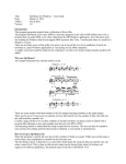
3.9. EVENT BUFFER DATA STRUCTURE
The readout from the active Buffer (i.e. the one pointed from the Read Pointer) of the
TDC chip provides the following words:
• a header that contains the event counter value;
• the data words containing the 16 bit converted time values, the channel number
and two status bits (edge, overflow); the last word will be identified by the
condition that Event Buffer <30> =1 (see § 4.22).
The board adds to these words some further information:
• TDC number (1 bit);
• Valid Data (1 bit).
Page 16 of 39
23/01/03
V673A User's Manual
Version 1.1
The following figure shows an example of the Event Buffer structure (see Fig. 4.18 for
the exact meaning of the bits):
31 30 29 28 27 26 25 24 23 22 21 20 19 18 17 16 15 14 13 12 11 10 9
8
7
6
Read Pointer = n
0
0
1
1
TDC chip n. 1
ch. 2 and ch.5 converted
0
0
1
0
0
0
0
1
0
0
1
0
1
1
0
0
0
1
0
1
0
1
Read Pointer = n+1
0
0
1
1
TDC chip n. 1
0
0
1
0
0
0
0
0
0
0
1
ch. 0, 1and 3 converted
ch. 1 has 2 hits
0
0
1
0
0
0
0
0
1
0
1
CONVERTED DATUM
0
0
1
0
0
0
0
0
1
0
1
CONVERTED DATUM
0
1
1
0
0
0
0
1
1
0
1
CONVERTED DATUM
5
4
EVENT COUNTER
CONVERTED DATUM
CONVERTED DATUM
EVENT COUNTER
CONVERTED DATUM
Fig. 3.2: Mod. V673A Multievent Buffer Data StructureErrore. Il segnalibro non è
definito.
N.B.: Due to the TDC chip internal structure, during the readout of an event (everything
that comes in between a Header and a Last Datum word) no access is allowed to all
registers of the TDC, except for the following (relevant to the board): Module Identifier
(§4.3), Interrupt Register (§4.4) and Board Status Register (§ 4.5).
3.10. READOUT OPERATING MODES
For what concerns the readout modes, the KLOE TDC chip can operate in two different
readout modes:
- SEQUENTIAL READOUT: the Event Buffers are read out sequentially and the read
pointer is automatically incremented.
The initialization of the module involves the following settings:
ASKEV=0 in the Main Control Registers for all 2 TDC chips
(Address Base + %12, %16).
In this way all the acquired events can be read out the buffers readout can occur in
random mode at addresses %104 and %10A and in Block Transfer mode at %100.
- EVENT REQUEST READOUT: via VME is it possible to ask for the data coming from a
given event number. The comparison between the event numbers is performed on a
programmable number of bits, in order to allow event counting in experiments using less
than 16 bits to identify events.
The initialization of the module involves the following settings:
ASKEV=1 in the Main Control Registers (see §4.7) for all 4 TDC chips .
EVNWIDTH = n, where n is the significant number of bits minus one of the comparison
with the event counter in the Main Control Registers (see §4.7) for all 2 TDC chips .
Once performed these settings, an event request is done by writing the desired event
number in the address %0008 (see %4.6). This causes the following actions:
•
•
the /No_data flags are set (see § 4.5);
If the event is present (/No_Data flag to 1) the read pointer is set to the Event Buffer
containing that particular event and all the Event Buffers containing a smaller event
number are released;
Page 17 of 39
3
2
1
0
23/01/03
V673A User's Manual
Version 1.1
After the event request, the readout can be performed only in Block Transfer Mode as
described in §3.12 here below.
3.11. BLOCK TRANSFER MODE (Sequential Readout)
The module supports the Standard BLT32 mode. A Block Transfer cycle occurs by read
accessing the Address Base + %100 in BLT32 mode and involves the readout of the
buffers of all TDC chips that have data.
Once the Block Transfer cycle is issued, a Block Transfer Control Logic freezes the
status of the empty flags, thus knowing which TDCs have data to read out. The Control
Logic assigns a priority readout and reads a single event for each TDC that contains
data, starting fron the TDC 0 to the TDC 1.
It is not obvious that two TDCs provide data that belong to the same event (see Fig. 3.3):
if, e.g., TDC chip 0 has data relevant to events 0, 1, 3 and 5 and TDC 1 has data
relevant to events 1 and 3, a Block Transfer readout will return data from the 2 TDCs
with different event numbers. It is care of the User to check consistency of event
numbers and eventually build its own event from the single data.
TDC0
3
2
1
0
TDC1
5
3
1
0
BUFFER
3
2
1
0
EVENT
BLT NR. 1
TDC 0
TDC 1
0
1
BERR
3
1
BLT NR. 2
TDC 0
TDC 1
1
3
BERR
BLT NR. 3
TDC 0
3
BERR
BLT NR. 4
TDC 0
5
BERR
BLOCK TRANSFER READOUT
Fig. 3.3: Mod. V673A Buffers Readout SchemeErrore. Il segnalibro non è definito.
A standard readout could be a Block Transfer with the maximum possible length for the
relevant event (1026 words: 2 headers + 64x16 data words) and use the VME Bus Error
(BERR) feature: the module must have the BERR_ENABLE bit set to 1 in the
Board_Status_Register (see §4.5). When a Block Transfer is performed, with the
readout of the word that follows the last word (read out from the last not empty TDC) a
VME Bus Error will be generated and the Block Transfer cycle is aborted. This feature is
very useful if the VME CPU handles the Bus Error in an efficient way.
If the Bus Error feature cannot be used for this purpose, a Block Transfer can still be
performed. The module must have the BERR_ENABLE bit set to 0 in the
Board_Status_Register (see §4.5). It can be useful to remember that each Block
Transfer is composed as a matter of fact of a certain number of bursts. Each burst
transfers at most 256 bytes (64 long words) and this number is programmable in the
VME CPU. In the previous Block Transfer readout (with Bus Error), the timing diagram of
the readout (as seen on the VME bus) is the following:
Page 18 of 39
23/01/03
V673A User's Manual
Version 1.1
BUS ERROR ENABLED
BURST
VME AS
VME DATA
VME BERR
EMPTY FLAG
FREEZING
BUS ERROR
EMPTY FLAG
FREEZING
Fig. 3.4: Mod. V673A Block Transfer with Bus ErrorErrore. Il segnalibro non è
definito.
In the current Block Transfer readout (without Bus Error), the timing diagram of the
readout is the following:
BUS ERROR DISABLED
VME AS
BURST
VME DATA
EMPTY FLAG
FREEZING
NOT VALID
DATA
EMPTY FLAG
FREEZING
Fig. 3.5: Mod. V673A Block Transfer without Bus ErrorErrore. Il segnalibro non è
definito.
The two readouts are more or less the same, i.e. the Block Transfer cycle is always
completed, but in the former case the Bus Error terminates the cycle, while in the latter
case the burst that would have been interrupted by a Bus Error causes a readout of
dummy (not valid) data, that can be recognized in the offline by the bit 31 of the data
word (see § 4.21). In the former case it is convenient to perform a Block Transfer with
the highest number of transferred words (e.g. 1026), while in the latter it is convenient, in
order to minimize the not valid words, to tailor the number of transferred words
considering both the average hit occupancy of each event and the rate of events (the
more hit occupancy and rate, the more the Block transfer length).
N.B.: Due to the TDC chip internal structure, during the readout of an event (everything
that comes in between a Header and a Last Datum word) no access is allowed to all
registers of the TDC, except for the following (relevant to the board): Module Identifier
(§4.3), Interrupt Register (§4.4) and Board Status Register (§ 4.5). If the User wishes to
change any TDC setting during or after a Block Transfer with Bus error disabled, he/she
must interrupt completely the acquisition (e.g. with a Clear All Buffers command): an
event may be lost in this way.
In both readout modes the Block Tranfer could be performed either by checking the Data
Present bit in the Board Status Register (see §4.5) or by enabling the Interrupt (see
§5.1).
Page 19 of 39
23/01/03
V673A User's Manual
Version 1.1
3.12. BLOCK TRANSFER MODE (Event Request Readout)
In Event Request Readout (see §1.2.4), the Standard BLT32 mode is the only way to
read data in the buffers. The User should set the ASKEV bit in the Main A Block Transfer
cycle occurs by read accessing the Address Base + %180 in BLT32 mode and involves
the readout of the buffers of all TDC chips that have data.
Once the Block Transfer cycle is issued, a Block Transfer Control Logic freezes the
status of the No Data flags, thus knowing which TDCs have data to read out. The
Control Logic assigns a priority readout and reads the requested event for each TDC
that contains data, starting fron the TDC 0 to the TDC 1.
The readout of the data in the buffers can be performed according to the procedure
described in the previous paragraph (§3.10).
N.B.: If the readout of the event n requires more than one burst, as shown in Fig. 3.43.5, the User must take care of performing the same event request, i.e. for the same
event n (Access to base + 0x0008) between two bursts of the Block Transfer cycle.
3.13. EXAMPLE OF AN INITIALIZATION
Here below is described an example of a simple initialization of the module.
1) Write %F53F in the Main Control Registers for all 2 TDC chips
(Address Base + %12, %16).
This operation sets the TDCs in the following status:
NHITS=15 (maximum 16 hits);
CKMODE=1 (Internal Clock Mode enabled);
CKDIS=1 (Clock disabled);
TDCMODE=0 (Common Start selected);
ASKEV=0 (sequential readout mode);
SMODE= 1 (rising edge only);
TEST=1 (test mode ON);
EVNWIDTH=15 (16 bits Event Counter).
2) Perform a Clear All Buffers (Access to address Base + %078)
This operation acts on all TDCs.
3) Write a value of %003x in the Counter Range Registers for all 2 TDC chips, where x
sets the Counter Range as described in §4.8.
(Address Base + %1A, %1E).
If Common Start mode is selected, the CRANGE value must be the smallest value
that exceeds the COMM signal length (= measurement gate). E.g. if the COMM
signal is 500 ns, the CRANGE must be 512 ns, i.e. x=8.
Write %001A in the Clock Control Registers for all 2 TDC chips
(Address Base + %92, %96).
4) Perform a Begin DLL (Access to address Base + %110).
This operation starts the DLL on all TDCs.
Perform a Clear All Buffers (Access to address Base + %078).
This operation acts on all TDCs.
Page 20 of 39
23/01/03
V673A User's Manual
Version 1.1
5) Write %F11F in the Main Control Registers for all 2 TDC chips
(Address Base + %12, %16).
This operation sets the TDCs in the following status:
NHITS=15 (maximum 16 hits);
CKMODE=1 (Internal Clock Mode enabled);
CKDIS=0 (Clock enabled);
TDCMODE=0 (Common Start selected);
ASKEV=0 (sequential readout mode);
SMODE= 1 (rising edge only);
TEST=0 (test mode OFF);
EVNWIDTH=15 (16 bits Event Counter).
Write %FFFF in the Mask Registers for all 2 TDC chips
(Address Base + %32, %36, %B2 and %B6).
This operation enables all channels for all TDCs.
Similar initializations can be performed for different operating modes.
N.B.: During initialization phase no hits must arrive either on the single channels
or on the COMM input.
Page 21 of 39
23/01/03
V673A User's Manual
Version 1.1
4. VME INTERFACE
4.1. ADDRESSING CAPABILITY
The module works in A24/A32 mode. This implies that the module's address must be
specified in a field of 24 or 32 bits. The Address Modifiers code recognized by the
module are:
AM=%3F:
AM=%3D:
AM=%3B:
AM=%39:
AM=%0F:
AM=%0D:
AM=%0B:
AM=%09:
A24 supervisory block transfer (BLT)
A24 supervisory data access
A24 user block transfer (BLT)
A24 user data access
A32 supervisory block transfer (BLT)
A32 supervisory data access
A32 user block transfer (BLT)
A32 user data access
The module's Base Address is fixed by 4 internal rotary switches housed on two piggyback boards plugged into the main printed circuit board.
The Base Address can be selected in the range:
% 00 0000
<->
% FF 0000
A24 mode
% 0000 0000
<->
% FFFF 0000
A32 mode
The Address Map of the page is shown in Table 4.1.
4.2. DATA TRANSFER CAPABILITY
The internal registers are accessible in D16 mode, unless otherwise specified. Access in
D32 and D32BLT is available for the event buffers.
Page 22 of 39
23/01/03
V673A User's Manual
Version 1.1
Base address bit <23..20>
Base address bit <19..16>
Base address bit <31..28>
Base address bit <27..24>
Fig. 4.1: Mod. V673A Base Address SettingErrore. Il segnalibro non è definito.
Page 23 of 39
23/01/03
V673A User's Manual
Version 1.1
Table 4.1: Address Map for the Mod. V673AErrore. Il segnalibro non è definito.
ADDRESS
REGISTER/CONTENT
TYPE
ACCESS TYPE
Base + 0x0000
Base + 0x0002
INTERRUPT VECTOR AND LEVEL
BOARD STATUS
r/w
r/w
D16
D16
Base + 0x0008
REQUESTED EVENT
w
D16
Base + 0x0012
Base + 0x0016
MAIN CONTROL ch. 0..31
MAIN CONTROL ch. 32..63
r/w
r/w
D16
D16
Base + 0x001A
Base + 0x001E
COUNTER RANGE ch. 0..31
COUNTER RANGE ch. 32..63
r/w
r/w
D16
D16
Base + 0x0022
Base + 0x0026
EVENT NUMBER ch. 0..31 *
EVENT NUMBER ch. 32..63 *
r/w
r/w
D16
D16
Base + 0x002A
Base + 0x002E
TDC COUNTER ch. 0..31 *
TDC COUNTER ch. 32..63 *
r/w
r/w
D16
D16
Base + 0x0032
Base + 0x0036
MASK ch. 0..15
MASK ch. 32..47
r/w
r/w
D16
D16
Base + 0x003A
Base + 0x003E
Base + 0x0042
Base + 0x0046
Base + 0x004A
Base + 0x004E
Base + 0x0052
Base + 0x0056
EMPTY FLAG BUFFER 0 ch. 0..15
EMPTY FLAG BUFFER 0 ch. 32..47
EMPTY FLAG BUFFER 1 ch. 0..15
EMPTY FLAG BUFFER 1 ch. 32..47
EMPTY FLAG BUFFER 2 ch. 0..15
EMPTY FLAG BUFFER 2 ch. 32..47
EMPTY FLAG BUFFER 3 ch. 0..15
EMPTY FLAG BUFFER 3 ch. 32..47
r
r
r
r
r
r
r
r
D16
D16
D16
D16
D16
D16
D16
D16
Base + 0x005A
Base + 0x005E
EVENT # BUFFER 0 ch. 0..31 *
EVENT # BUFFER 0 ch. 32..63 *
r/w
r/w
D16
D16
Base + 0x0062
Base + 0x0066
COMMON BUFFER 0 ch. 0..31
COMMON BUFFER 0 ch. 32..63
r
r
D16
D16
Base + 0x006A
Base + 0x006E
CLEAR CURRENT BUFFER ch. 0..31 *
CLEAR CURRENT BUFFER ch. 32..63 *
Base + 0x0072
Base + 0x0076
POINTERS ch. 0..31
POINTERS ch. 32..63
r
r
D16
D16
Base + 0x0078
Base + 0x0088
CLEAR ALL BUFFERS ch. 0..63
INTERNAL STOP ch. 0..63 *
*
*
D16
D16
Base + 0x0092
Base + 0x0096
CLOCK CONTROL ch. 0..31 *
CLOCK CONTROL ch. 32..63 *
r/w
r/w
D16
D16
Base + 0x00B2
Base + 0x00B6
MASK ch. 16..31
MASK ch. 48..63
r/w
r/w
D16
D16
Page 24 of 39
D16
D16
23/01/03
V673A User's Manual
Version 1.1
Base + 0x00BA
Base + 0x00BE
Base + 0x00C2
Base + 0x00C6
Base + 0x00CA
Base + 0x00CE
Base + 0x00D2
Base + 0x00D6
EMPTY FLAG BUFFER 0 ch. 16..31
EMPTY FLAG BUFFER 0 ch. 48..63
EMPTY FLAG BUFFER 1 ch. 16..31
EMPTY FLAG BUFFER 1 ch. 48..63
EMPTY FLAG BUFFER 2 ch. 16..31
EMPTY FLAG BUFFER 2 ch. 48..63
EMPTY FLAG BUFFER 3 ch. 16..31
EMPTY FLAG BUFFER 3 ch. 48..63
r
r
r
r
r
r
r
r
D16
D16
D16
D16
D16
D16
D16
D16
Base + 0x00DA
Base + 0x00DE
EVENT # BUFFER 1 ch. 0..31
EVENT # BUFFER 1 ch. 32..63
r/w
r/w
D16
D16
Base + 0x00E2
Base + 0x00E6
COMMON BUFFER 1 ch. 0..31
COMMON BUFFER 1 ch. 32..63
r
r
D16
D16
Base + 0x0100
Base + 0x0104
Base + 0x010C
SEQUENTIAL READOUT ch. 0..63
SEQUENTIAL READOUT ch. 0..31
SEQUENTIAL READOUT ch. 32..63
r
r
r
D32 BLT
D32
D32
Base + 0x0110
BEGIN DLL *
Base + 0x015A
Base + 0x015E
EVENT # BUFFER 2 ch. 0..31 *
EVENT # BUFFER 2 ch. 32..63 *
r/w
r/w
D16
D16
Base + 0x0162
Base + 0x0166
COMMON BUFFER 2 ch. 0..31
COMMON BUFFER 2 ch. 32..63
r
r
D16
D16
Base + 0x0180
Base + 0x0190
REQUEST MODE READOUT ch. 0..63
RESTART DLL *
r
D32 BLT
D16
Base + 0x01DA
Base + 0x01DE
EVENT # BUFFER 3 ch. 0..31 *
EVENT # BUFFER 3 ch. 32..63 *
r/w
r/w
D16
D16
Base + 0x01E2
Base + 0x01E6
COMMON BUFFER 3 ch. 0..31
COMMON BUFFER 3 ch. 32..63
r
r
D16
D16
Base + 0x01F0
CLEAR TDC
Base + 0x01FA
Base + 0x01FC
Base + 0x01FE
FIXED CODE
MANUFACTURER & MODULE TYPE
VERSION & SERIAL NUMBER
D16
D16
*: Available in TEST MODE only
Page 25 of 39
r
r
r
D16
D16
D16
23/01/03
V673A User's Manual
Version 1.1
4.3. MODULE IDENTIFIER WORDS
(Base address + %1FA ,+%1FC, +%1FE read only)
The Three words located at the highest address on the page are used to identify the
module as shown in figure 5.2:
15 14 13 12 11 10 9
V e r s i o n
8
M o d u l e ' s
Manufacturer number
% F A
F i x e d
7
6
5
s e r i a l
M o d u l e
c o d e
4
% F 5
3
2
1
Address
Base + % 1FE
n u m b e r
Base + % 1FC
t y p e
F i x e d
0
Base + % 1FA
c o d e
Fig. 4.2: Module Identifier WordsErrore. Il segnalibro non è definito.
At the address Base + % 1FA the two particular bytes allow the automatic localization of
the module. For the Mod. V673A the word at address Base + % 1FC has the following
configuration:
Manufacturer N°=
Type of module =
000010 b
0100101101 b
The word located at the address Base + %1FE identifies the single module via a serial
number, and any change in the hardware will be shown by the Version number.
4.4. INTERRUPT VECTOR AND LEVEL REGISTER
(Base address + %0000 read/write)
This register contains the value of the Interrupt STATUS/ID that the V673A
INTERRUPTER (see § 5) places on the VME data bus during the Interrupt Acknowledge
cycle. Bits <10..8> of this register contain the value of the interrupt level (Bits 11 to 15
are meaningless).
15 14 13 12 11 10 9
8
7
LEV<2..0>
6
5
4
3
2
1
0
STATUS /I D
Interrupt STATUS/ID
Interrupt Level
Fig. 4.3: Mod. V673A Interrupt Vector & Level Register
Errore. Il segnalibro non è definito.
4.5. BOARD STATUS REGISTER
(Base address + %0002 read/write)
This register contains information on the status of the module and the TDC chips. All bits
are accessible in read only, except for the BERR_ENABLE that is accessible in
read/write mode.
Page 26 of 39
23/01/03
V673A User's Manual
Version 1.1
15 14 13 12 11 10 9
8
7
6
5
4
3
2
1
0
/NO_DATA
/EM_BUF
/FU_BUFF
/BUSY
/FULL
BERR_EN
DATA_PRESENT
Fig. 4.4: Mod. V673A Board Status RegisterErrore. Il segnalibro non è definito.
/NO_DATA
No Data bits (one per TDC chip: 1=TDC chip 0; 3=TDC chip 1)
Valid in Request Mode only. After a trigger request it returns information
on the event existence:
=0
requested event not present in the TDC chip buffers;
=1
requested event is present in the TDC chip buffers;
/EM_BUF
Not Empty Buffer bits (one per TDC chip: 5=TDC chip 0; 7=TDC chip 1)
=0
no data present in the TDC chip buffers;
=1
at least one datum is present in at least one of the TDC chip
buffers;
/FU_BUF
Not Full Buffer bits (one per TDC chip: 9=TDC chip 0; 11=TDC chip 1)
=0
all the TDC chip buffers are full;
=1
at least one of the TDC chip buffers is empty;
/BUSY
Not Busy bit.
=0
the board is busy;
=1
the board is Not busy;
/FULL
Not Full bit.
=0
the board is full;
=1
the board is Not full;
BERR_EN
Bus Error Enable (enables the Bus Error generation on the board)
To be used for Block Transfer mode only.
=0
Bus Error Not Enabled
=1
Bus Error Enabled
DATA_PRESENT
Data Present bit.
=0
no data present in all TDC chips' buffers;
=1
at least one datum is present in at least one of the TDC
chip buffers;
Page 27 of 39
23/01/03
V673A User's Manual
Version 1.1
4.6. REQUESTED EVENT REGISTER
(Base address + %08 write only)
This 16-bit register allows to ask for the desired event to be read out from the KLOE
TDC chips. It can be used in Request Mode only. The request is performed for all chips.
15 14 13 12 11 10 9
8
7
6
5
4
3
2
1
0
EVENT NUMBER
EVN#
Fig. 4.5: Mod. V673A Requested Event RegisterErrore. Il segnalibro non è definito.
4.7. MAIN CONTROL REGISTER
(Base address + %12 and %16, read/write)
These registers allow the main control of the KLOE TDC chips. Address %12 refers to
TDC chip 0, %16 refers to TDC chip 1.
15 14 13 12 11 10 9
8
7
6
5
4
3
2
1
0
NHITS
CKMODE
CKDIS
TDCMODE
ASKEV
SMODE
TEST
EVNWIDTH
Fig. 4.6: Mod. V673A Main Control RegisterErrore. Il segnalibro non è definito.
NHITS:
Maximum number of hits allowed per event.
=0: 1 event;
=15: 16 events.
CKMODE:
The TDC clock can be internally generated, out of an external clock
working at moderate frequencies, or externally at the full working
frequency. When CKMODE is set the internal clock is chosen.
CKDIS:
For debug purposes the clock can be disabled by setting the CKDIS flag.
TDCMODE:
The TDC can work both in common START or common STOP mode. If
TDCMODE is set the TDC works in common STOP mode.
ASKEV:
The readout of the chip can be done in two different ways, simply by
emptying all the event buffers in order (Sequential Mode) or by asking for
a particular event number (Event Request Mode). If the ASKEV flag is set
the TDC is set in Event Request Readout Mode.
SMODE:
It is foreseen to record rising edges, falling edges or both, depending on
the setting of the signal mode register (see table here below).
Page 28 of 39
23/01/03
Signal Mode
Not Allowed
Rising Edge Only
Falling Edge Only
Both
Edges
Recorded
TEST:
V673A User's Manual
Version 1.1
bit 9 bit 8
0
0
0
1
1
0
1
1
all the registers inside the chip can be read or written. In order not to
disrupt the data during normal data taking due to a wrong operation, some
commands can be issued only after setting the TEST bit on.
EVNWIDTH: These four bits set the number of significant bits of the Event Registers
and of the Event Counter (EVNWIDTH=15 ⇒16 bit, EVNWIDTH=0 ⇒
1 bit), used in event request mode.
4.8. COUNTER RANGE REGISTER
(Base address + %1A and %1E, read/write)
These registers are used to define the maximum time span to be recorded into an event
buffer when operating in COMMON STOP (Bits 6 to 15 are meaningless). Address %1A
refers to TDC chip 0, %1E refers to TDC chip 1.
15 14 13 12 11 10 9
8
7
6
5
4
3
2
1
0
NBITS
DEPTH_COMP
Fig. 4.7: Mod. V673A Counter Range RegisterErrore. Il segnalibro non è definito.
NBITS:
number of effective counter bits; allowed values are 4 to 14.
The effective time span T is
(allowed values approx. 32 ns to 32 µs) :
T = (2NBITS+1 )* (TDC LSB) ns
(e.g. NBITS=6 ⇒ T = 64*1.0416 ns)
DEPTH_COMP:
depth of comparison of old event elimination. Indicates how often
a comparison is performed. These bits must be both set at 1,
giving 32 ns.
N.B.: If Common Start mode is selected, the CRANGE value must be set as the
smallest value that exceeds the COMM signal length (= measurement gate). E.g. if
the COMM signal is 500 ns, the CRANGE must be 512 ns, i.e. NBITS=8.
Page 29 of 39
23/01/03
V673A User's Manual
Version 1.1
4.9. EVENT NUMBER REGISTER
(Base address + %22 and %26, read/write)
These 16-bit registers contain the total number of COMMON START/ STOP signals
received and accepted by the board and distributed to the chips; they can be used to
check the synchronization of different circuits: it must be the same number for all the
TDC chips. Address %22 refers to TDC chip 0, %26 refers to TDC chip 1. Write access
is available only if the TEST flag is set in the Main Control Register (see § 4.7).
15 14 13 12 11 10 9
8
7
6
5
4
3
2
1
0
EVENT NUMBER
Fig. 4.8: Mod. V673A Event Number RegisterErrore. Il segnalibro non è definito.
EVENT NUMBER:
number of total COMMON signals received by each TDC chip.
4.10. TDC COUNTER REGISTER
(Base address + %2A and %2E, read/write)
These 16-bit registers contain the value of the TDC chip gray counter at the moment in
which the VME command is issued. Address %2A refers to TDC chip 0, %2E refers to
TDC chip 1. Write access is available only if the TEST flag is set in the Main Control
Register (see § 4.7).
15 14 13 12 11 10 9
8
7
6
5
4
3
2
1
0
TDC COUNTER
Fig. 4.9: Mod. V673A TDC Counter RegisterErrore. Il segnalibro non è definito.
TDC COUNTER:
gray counter value of each TDC chip at command issue.
4.11. MASK REGISTER
(Base address + %32 and %36, Base address + %B2 and %B6, read/write)
These 16-bit registers allow to disable the single channels if needed. It must be
initialized before the acquisition. A bit set to 1 enables the relevant channel. Address
%32 refers to the 16 lower channels of TDC chip 0, %36 to the 16 higher channels of
TDC chip 0. Address %B2 refers to the 16 lower channels of TDC chip 1, %B6 to the 16
higher channels of TDC chip 1.
15 14 13 12 11 10 9
8
7
6
5
4
3
2
MASK PATTERN
Fig. 4.10: Mod. V673A Mask Register
Errore. Il segnalibro non è definito.
Page 30 of 39
1
0
23/01/03
V673A User's Manual
Version 1.1
4.12. EMPTY FLAG REGISTERS
(Base address + %3A through %56, %BA through %D6, read only)
These 16-bit registers contain information on the occupation (Empty or Not Empty) of
each channel of each buffer of each TDC chip in the module. A bit set to 1 implies that
the relevant channel is Not Empty. For the exact corespondence between the addresses
and the channels please refer to Table 4.1. As an example, here below is the status of
this register at Base address + %3A (Buffer 0, Channel 0 to 15).
15 14 13 12 11 10 9
8
7
6
5
4
3
2
1
0
CH. 0
CH. 15
Fig. 4.11: Mod. V673A Empty Flag RegisterErrore. Il segnalibro non è definito.
4.13. EVENT # BUFFER 0 REGISTER
(Base address + %5A and %5E, read/write)
These 16-bit registers provide the Event number contained in buffer 0 (see § 1.2.2).
Address %5A refers to TDC chip 0, %5E refers to TDC chip 1. Write access is available
only if the TEST flag is set in the Main Control Register (see § 4.7).
15 14 13 12 11 10 9
8
7
6
5
4
3
2
1
0
EVENT NUMBER
Fig. 4.12: Mod. V673A Event # Buff. 0 RegisterErrore. Il segnalibro non è definito.
EVENT NUMBER:
number of event contained in Event Buffer 0.
4.14. COMMON BUFFER 0 REGISTER
(Base address + %62 and %66, read only)
These 16-bit registers contain, for event buffer 0, the value of the TDC chip gray counter
at the moment in which the COMMON input has been issued. Address %62 refers to
TDC chip 0, %66 refers to TDC chip 1.
15 14 13 12 11 10 9
8
7
6
5
4
3
2
1
0
TDC COUNTER
Fig. 4.13: Mod. V673A Common Buff. 0 RegisterErrore. Il segnalibro non è definito.
TDC COUNTER:
gray counter value of each TDC chip at command issue.
Page 31 of 39
23/01/03
V673A User's Manual
Version 1.1
4.15. CLEAR CURRENT BUFFER
(Base address + %6A and %6E)
A dummy access to this location clears the current buffer, i.e. the one pointed by the
Read Pointer. The Read Pointer is automatically incremented. Address %6A refers to
TDC chip 0, %6E refers to TDC chip 1.
4.16. POINTERS REGISTER
(Base address + %72 and %76, read only)
These registers contain, for each TDC chip, the position of the read and write pointers,
plus some additional information for CAEN Internal use only (Bits 7 to 15 are
meaningless). Address %72 refers to TDC chip 0, %76 refers to TDC chip 1.
15 14 13 12 11 10 9
8
7
6
5
4
3
2
1
0
READ POINTER
WRITE POINTER
RESERVED
Fig. 4.14: Mod. V673A Pointer RegisterErrore. Il segnalibro non è definito.
READ POINTER:
active event buffer in readout.
WRITE POINTER:
active event buffer in writing.
RESERVED:
CAEN Internal use only.
4.17. CLEAR ALL BUFFERS
(Base address + %78)
A dummy access to this location clears all the TDC buffers for all TDCs.
4.18. INTERNAL STOP
(Base address + %88)
A dummy access to this location generates an internal STOP for test purposes. Access
is available only if the TEST flag is set in the Main Control Register (see § 4.7). The
STOP is issued to all channels at the time of the VME command arrival.
Page 32 of 39
23/01/03
V673A User's Manual
Version 1.1
4.19. CLOCK CONTROL REGISTER
(Base address + %92 and %96, read/write)
These registers allow the CLOCK control of the KLOE TDC chips. For test purposes, it is
possible to access the CKOUT pin of the TDC chips with an oscilloscope probe. Bits 4
and 5 of the MAIN CONTROL register must also be used (see below). Address %92
refers to TDC chip 0, %96 refers to TDC chip 1. Write access is available only if the
TEST flag is set in the Main Control Register (see § 4.7).
15 14 13 12 11 10 9
8
7
6
5
4
3
2
1
0
RESERVED
CK_FHALF
CKVALPAD
CKVALPADN
CKPADEXT
CKSOURCEMUL
Fig. 4.15: Mod. V673A Clock Control RegisterErrore. Il segnalibro non è definito.
CK_FHALF: Halves the frequency of the DLL.
=0: External CLOCK enabled.
=1: Half frequency DLL output enabled.
CKVALPAD: CKOUT output enable/disable.
=0: CKOUT disabled.
=1: CKOUT enabled.
CKVALPADN: CKOUT_N output enable/disable.
=0: CKOUT_N disabled.
=1: CKOUT_N enabled.
CKPADEXT: CKOUTcontrol.
=00: CKOUT = "1".
=01: CKOUT = Reference CLOCK.
=10: CKOUT = External CLOCK.
=11: CKOUT = Internal TDC chip CLOCK.
CKSOURCEMUL:
CKOUT_N output enable/disable.
=0: 160 MHz clock input to DLL.
=1: External clock input to DLL.
E.g., to see the 160 MHz, the 480 MHz or the External CLOCK, the clock register and
the main control register must be set as follows:
• 160 MHz CLOCK: CLOCK_CONTROL[15:10] = "01011x",
MAIN_CONTROL[5:4] = "01";
• 480 MHz CLOCK: CLOCK_CONTROL[15:10] = "01111x",
MAIN_CONTROL[5:4] = "01";
• Ext. CLOCK: CLOCK_CONTROL[15:10] = "x01110",
MAIN_CONTROL[5:4] = "00".
Page 33 of 39
23/01/03
V673A User's Manual
Version 1.1
4.20. EVENT # BUFFER 1 REGISTER
(Base address + %DA and %DE, read/write)
These 16-bit registers provide the Event number contained in buffer 1 (see § 1.2.2).
Address %DA refers to TDC chip 0, %DE refers to TDC chip 1. Write access is available
only if the TEST flag is set in the Main Control Register (see § 4.7).
15 14 13 12 11 10 9
8
7
6
5
4
3
2
1
0
EVENT NUMBER
Fig. 4.16: Mod. V673A Event # Buff. 1 RegisterErrore. Il segnalibro non è definito.
EVENT NUMBER:
number of event contained in Event Buffer 1.
4.21. COMMON BUFFER 1 REGISTER
(Base address + %E2 and %E6, read only)
These 16-bit registers contain, for event buffer 1, the value of the TDC chip gray counter
at the moment in which the COMMON input has been issued. Address %E2 refers to
TDC chip 0, %E6 refers to TDC chip 1.
15 14 13 12 11 10 9
8
7
6
5
4
3
2
1
0
TDC COUNTER
Fig. 4.17: Mod. V673A Common Buff. 1 RegisterErrore. Il segnalibro non è definito.
TDC COUNTER:
gray counter value of each TDC chip at command issue.
4.22. SEQUENTIAL READOUT
(Base address + %104, %10C read only, D32)
In Sequential Readout mode, after the readout of an event, the Read Pointer is
automatically incremented.
The Data Words contain the 16 bit converted values together with the corresponding 5
bit channel number, the edge type bit (rising or falling), the overflow bit and some
additional informations.
31 30 29 28 27 26 25 24 23 22 21 20 19 18 17 16 15 14 13 12 11 10
/V LD
T#
ED
CHANNEL #
OV
E
9
8
7
6
5
4
3
2
1
0
TDC DATA WORD
TDC Data Word
Edge Type
Overflow
Channel number
Event/ Datum
TDC Number
RESERVED
Last Datum
Not Valid Datum
Fig. 4.18: Mod. V673A Output Buffer Data WordErrore. Il segnalibro non è definito.
Page 34 of 39
23/01/03
V673A User's Manual
Version 1.1
TDC DATA WORD:
contains either the TDC counter value or Event Number,
depending on bit 23 of this register (EVENT/DATUM flag).
EDGE TYPE FLAG:
0 = rising, 1 = falling.
OVERFLOW FLAG:
1 = more than the programmable number of hits has reached the
board's inputs.
CHANNEL NUMBER: Channel number (0 to 31) of the current datum within
the current chip (indicated in the TDC number, bits 25 and 24).
EVENT/DATUM:
Event or Datum flag.
ED=0 ⇒ the word currently read is a TDC datum.
ED=1 ⇒ the word currently read is an event number.
TDC NUMBER:
Number of TDC chip to which the datum belongs.
0=CH. 0 to 31;
1=CH. 32 to 63.
LAST DATA:
LAST DATA flag.
LD=1 ⇒ the word currently read is the last
belonging to the current event.
NOT VALID DATUM: Used in Block Transfer mode.
/V=0 ⇒ Valid Datum.
/V=1 ⇒ Not Valid Datum (the data word is meaningless).
4.23. BEGIN DLL
(Base address + %110)
A dummy access to this location starts the Digital Locked Loop.
4.24. EVENT # BUFFER 2 REGISTER
(Base address + %15A and %15E, read/write)
These 16-bit registers provide the Event number contained in buffer 2 (see § 1.2.2).
Address %15A refers to TDC chip 0, %15E refers to TDC chip 1. Write access is
available only if the TEST flag is set in the Main Control Register (see § 4.7).
15 14 13 12 11 10 9
8
7
6
5
4
3
2
1
0
EVENT NUMBER
Fig. 4.19: Mod. V673A Event # Buff. 2 RegisterErrore. Il segnalibro non è definito.
EVENT NUMBER:
number of event contained in Event Buffer 2.
Page 35 of 39
23/01/03
V673A User's Manual
Version 1.1
4.25. COMMON BUFFER 2 REGISTER
(Base address + %162 and %166, read only)
These 16-bit registers contain, for event buffer 2, the value of the TDC chip gray counter
at the moment in which the COMMON input has been issued. Address %162 refers to
TDC chip 0, %166 refers to TDC chip 1.
15 14 13 12 11 10 9
8
7
6
5
4
3
2
1
0
TDC COUNTER
Fig. 4.20: Mod. V673A Common Buff. 2 RegisterErrore. Il segnalibro non è definito.
TDC COUNTER:
gray counter value of each TDC chip at command issue.
4.26. REQUEST MODE READOUT
(Base address + %180 read only, D32 BLK)
An access to this address in D32 BLK mode only causes the readout of the requested
event as described in §3.10. The structure of the data word is the same as in §4.22.
4.27. RESTART DLL
(Base address + %190)
A dummy access to this location restarts the Digital Locked Loop.
4.28. EVENT # BUFFER 3 REGISTER
(Base address + %1DA and %1DE, read/write)
These 16-bit registers provide the Event number contained in buffer 3 (see § 1.2.2).
Address %1DA refers to TDC chip 0, %1DE refers to TDC chip 1. Write access is
available only if the TEST flag is set in the Main Control Register (see § 4.7).
15 14 13 12 11 10 9
8
7
6
5
4
3
2
1
0
EVENT NUMBER
Fig. 4.21: Mod. V673A Event # Buff. 3 RegisterErrore. Il segnalibro non è definito.
EVENT NUMBER:
number of event contained in Event Buffer 3.
Page 36 of 39
23/01/03
V673A User's Manual
Version 1.1
4.29. COMMON BUFFER 3 REGISTER
(Base address + %1E2 and %1E6, read only)
These 16-bit registers contain, for event buffer 3, the value of the TDC chip gray counter
at the moment in which the COMMON input has been issued. Address %1E2 refers to
TDC chip 0, %1E6 refers to TDC chip 1.
15 14 13 12 11 10 9
8
7
6
5
4
3
2
1
0
TDC COUNTER
Fig. 4.22: Mod. V673A Common Buff. 3 RegisterErrore. Il segnalibro non è definito.
TDC COUNTER:
gray counter value of each TDC chip at command issue.
4.30. CLEAR TDC
(Base address + %1F0)
A dummy access to this location clears the TDC. It is equivalent to an external Reset.
Page 37 of 39
23/01/03
V673A User's Manual
Version 1.1
5. MOD. V673A INTERRUPTER
5.1. INTERRUPTER CAPABILITY
The Mod. V673A houses a VME RORA INTERRUPTER D08(o) type. This implies the
following:
• it responds to 8 bit, 16 bit and 32 bit interrupt acknowledge cycles providing an
8-bit STATUS/ID on the VME data lines D00..D07;
• it removes its interrupt request when some on board registers are accessed by
a VME MASTER (RORA: Release On Register Access).
5.2. INTERRUPT STATUS/ID
The interrupt STATUS/ID is 8 bit wide, and it is contained in the Interrupt Vector
Register<7..0>. The register is available at the VME address Base + % 00.
5.3. INTERRUPT LEVEL
The interrupt level corresponds to the value stored in the Interrupt Level Register
<10..8>. The register is available at the VME address Base + % 00. A value of 0 in the
Interrupt Level implies that no interrupt is generated.
5.4. INTERRUPT GENERATION
Via VME it is possible to program the Interrupt Generation on the condition that there are
data to read out in at least one chip (DATA_PRESENT in the Board Status Register set
to 1, see § 4.5).
5.5. INTERRUPT REQUEST RELEASE
The V673A INTERRUPTER removes its Interrupt request when the TDCs have been
completely read out (DATA_PRESENT set to 0).
Page 38 of 39
23/01/03
V673A User's Manual
Version 1.1
6. REFERENCES
[1] http://www.lnf.infn.it/kloe/
[2] M. Passaseo, E. Petrolo, S. Veneziano; A TDC integrated circuit for drift chamber
readout. Nuclear Instruments & Methods Phys. Res. A 367 (1995) 418-421.
See also http://sunset.roma1.infn.it/tdc/Welcome.html
[3] http://www.roma1.infn.it/labe/gia.html
[4] VMEbus Specification Manual Revision C.1, October 1985.
[5] G. Bianchetti et al., Specification for VMEbus CRATE Type V430, CERN-EP,
January 1990.
Page 39 of 39
23/01/03
V673A User's Manual
Version 1.1
APPENDIX A: ELECTRICAL DIAGRAMS
A.1