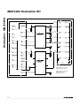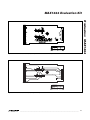
1
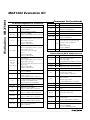
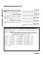
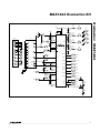
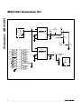
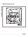
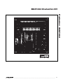
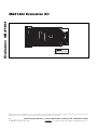
19-0582; Rev 0; 12/06
MAX1464 Evaluation Kit
The MAX1464 evaluation kit (EV kit) is designed to evaluate
the MAX1464 high-performance, low-power, low-noise
multichannel sensor signal processor. The EV kit
includes: an evaluation PCB, the EV board that contains
a MAX1464 signal conditioner with a typical application
circuit, and potentiometers that act as sensor inputs to
the MAX1464; an interface PCB, KEY, which acts as a
voltage level translator between the EV kit and the computer; a parallel-port extension cable; plus, supporting
software, program examples, and related documentation and application notes.
The DB25 pin connector allows a PC’s parallel port to
provide the interface. Two Windows®-based software
(hardware debugger and control program) provide a
friendly graphics user interface (GUI) to utilize the features of the MAX1464, as well as to perform sensor
compensation of one device. The Hardware Debugger
program includes multiple tabs for accessing relevant
registers and ports, writing programs to the on-chip flash
memory, downloading flash memory contents into a file,
etc. Use the Hardware Debugger program to learn the
MAX1464 functions and see the significance of individual registers and ports. The Control program includes
functional buttons to have the chip perform a series of
predefined lower level operations, such as pushing single buttons to read the ADC. The Control program can
be used to perform 2nd-order sensor compensation and
calibration.
The EV board can be powered by either a fixed +5V
supply or by an +8V to +40V supply that is regulated to
+5V by a regulator present on the EV kit board before it
is applied to the MAX1464 chip. Jumper JU1 must be
set consistently with the used power supply.
Order the MAX1464 EV kit for comprehensive evaluation
of the MAX1464 using a PC with an available parallel port.
Features
♦ Proven PCB Layout
♦ Windows 98/NT/2000/XP Compatible
♦ On-Board Potentiometers Act as Sensor Inputs
♦ Spare Area for Simple-Circuit Breadboarding
♦ LEDs for Visual Verification
♦ +5V or +8V to +40V Possible Supply
♦ Included Interconnect Cables
♦ Included Additional Samples
Ordering Information
PART
MAX1464EVKIT
MAX1464KEY
FILE
Digi-Key
800-344-4539 www.digikey.com
Methode
Electronics
708-867-6777 www.methode.com
Murata
800-831-9172 www.murata.com/cap
PacTec
610-361-4200 www.pactecenclosures.com
TDK
408-437-9585 www.component.tdk.com
Note: Indicate that you are using the MAX1464 when contacting these component suppliers.
—
OPERATION
Internal controls for learning
the MAX1464
Control program
Sensor compensation
—
Simple functions and
programming examples
—
Various related application notes
Component List
EV Kit Component List
REFERENCE QTY
DESCRIPTION
1
10µF ±20%, 10V tantalum
capacitor (1210)
TDK C3225X7R1C106M
Taiyo-Yuden LMK325BJ106MN
3
2.2µF ±10%, 10V X7R ceramic
capacitors (0805)
Murata GRM21BR71A225K
or equivalent
C3, C9
2
1µF ±10%, 10V X7R ceramic
capacitors (0805)
Murata GRM21BR71A105K
or equivalent
C4, C7,
C10–C13
6
0.1µF ±10%, 10V X7R ceramic
capacitors (0805)
Murata GRM21BR71E104K or equivalent
Component Suppliers
WEBSITE
28 SSOP
—
Hardware debugger
C1
PHONE
IC PACKAGE
0°C to +70°C
MAX1464 EV Kit Files
Windows is a registered trademark of Microsoft Corp.
SUPPLIER
TEMP RANGE
C2, C5, C8
________________________________________________________________ Maxim Integrated Products
For pricing, delivery, and ordering information, please contact Maxim/Dallas Direct! at
1-888-629-4642, or visit Maxim’s website at www.maxim-ic.com.
1
Evaluates: MAX1464
General Description
Evaluates: MAX1464
MAX1464 Evaluation Kit
Component List (continued)
EV Board Component List (continued)
REFERENCE QTY
C6
FB1, FB2
H1, H2
JU1, JU10
JU2, JU3,
JU4, JU8,
JU9,
JU11–JU14
LED1, LED2
P1
1
2
0Ω resistors (0805)
Digi-Key RL12T0.010JCT-ND or equivalent
2
14-pin headers
36-pin headers 0.01 centers (comes in
36-pin strips, cut to fit)
Sullins PTC36SAAN
Digi-Key S1012-36-ND
2
9
2
1
3-pin headers
36-pin headers 0.01 centers (comes in
36-pin strips, cut to fit)
Closed: JU1, pins 1-2, JU10,
pins 1-2
Sullins PTC36SAAN
Digi-Key S1012-36-ND
2-pin headers
36-pin headers 0.01 centers (comes in
36-pin strips, cut to fit)
Closed: JU2, JU4, JU8, JU9, JU11–JU14
Open: JU3
Sullins PTC36SAAN
Digi-Key S1012-36-ND
LEDs
Digi-Key P300-ND
2 x 8 male shrouded vertical ribbon
cable connector
Digi-Key MHB16K-ND or equivalent
P2
0
2 x 20 right-angle receptacle (not installed)
SAMTEC SSW-120-02-S-D-RA
Methode Electronics RS2R-40-G
RB1–RB4
4
Rubberband standoffs
R2
1
22Ω ±5% resistor (1206)
Digi-Key P22ECT-ND or equivalent
R4, R5
2
3kΩ ±5% resistors (1206)
Digi-Key P3.0KECT-ND or equivalent
R13–R16
4
10Ω ±1% resistors (1206)
Digi-Key P10RCT-ND or equivalent
R17
TB1, TB2
2
DESCRIPTION
0.001µF ±10%, 10V X7R ceramic
capacitor (0805)
Murata GRM216R71H102K
1
220Ω ±5% resistor (1206)
Digi-Key P220ECT-ND or equivalent
2
0.2in screw terminal blocks
Digi-Key ED1973
REFERENCE QTY
DESCRIPTION
U1
1
MAX1464AAI (28-pin SSOP)
U1
0
Factory option 28-pin SO socket
ENPLAS OTS-28(34)-0.65-1
U2
1
MAX6220ASA25 (8-pin SO)
U3
1
MAX6220ASA50 (8-pin SO)
VR1, VR2
2
20kΩ vertical adjust trimpots
Digi-Key 490-2323ND
—
13
Shunts
Closed: JU1 pins 1-2, JU2, JU4, JU8,
JU9, JU11–JU14, JU10 pins 1-2
Open: JU3
Sullins STC02SYAN
Digi-Key S9000-ND
—
1
MAX1464EVKIT PCB
Interface Board (KEY) Component List
REFERENCE QTY
DESCRIPTION
C1, C2
2
0.1µF ±10%, 50V ceramic
capacitors (1206)
Murata GRM319R71H104K or equivalent
C3, C4
0
Open
C5, C6
2
470pF ±10%, 10V ceramic capacitors
JU1
0
Leave open
P1
1
DB25 pin male connector, solder cup
Mount at edge of PCB
Digi-Key ET25P or equivalent
P2
1
2 x 8 male shrouded vertical ribbon
cable connector
Mount at edge of PCB
Digi-Key MHB16K-ND or equivalent
U1
1
MAX1841EUB
U2
1
Screw
1
MAX1841EUB
No. 2 56 x 1/2in Philips HD S/S machine
screw
Spacer
1
No. 2 aluminum round spacer,
1/4in length, unthreaded
Any
Spacer
1
No. 256 threaded 5/16in aluminum
round standoff
Digi-Key 1801CK-ND or equivalent
—
1
MAX1464KEY PCB
—
1
Snap-on plastic housing
PacTec K-CNM0406
Newark K-CNM-0406-BLACK
_______________________________________________________________________________________
MAX1464 Evaluation Kit
Required Equipment
•
MAX1464 EV kit
•
A fixed +5VDC power supply
•
Computer running Windows 98/NT/2000/XP with an
available parallel port (USB-to-parallel-port converters not supported)
•
A multimeter
•
One parallel (printer) cable
4) Press the Flash Memory tab in the Hardware
Debugger window.
5) Press Load Buffer from file tab.
6) Select … | MAX1464 | examples | cctmr1-64.hex
file to read the .hex file and save it in the temporary
buffer.
7) Press Write to device tab to write the cctmr1-64.hex
program to the flash memory.
8) Press Verify device against buffer to verify that the
flash memory write operation is successful.
Note: In the following sections, software-related items
are identified by bolding. Text in bold refers to items
directly from the EV kit software. Text in bold and
underlined refers to items from the Windows
98SE/2000/XP operating system.
9) Execute the LED double-blinking program by
pressing on the Run CPU button. The LEDs start
blinking. This process verifies that the EV kit connections are correct, the EV board jumpers are set
correctly, and the computer interface is working.
Procedures
Example of Using the Control Program
Note: Exit the Hardware Debugger before starting the
Control program.
This section demonstrates how to start the Control
program and make the basic measurement of the input
voltage.
1) Start the Control program from Start | MAX1464
EV kit | Control Program.
Applying Power to the MAX1464 EV Board
1) Verify that all jumpers on the EV kit board are set
per the default setting shown in Table 1.
2) Connect a fixed +5V power supply to the EV kit
board TB2 +5V terminal.
3) The LEDs on the EV kit board start blinking. The
MAX1464 EV kit is shipped with a program,
EVTEST1.hex, preloaded in the MAX1464 flash
memory. This program alternatively flashes the two
LEDs on the EV board.
Setting Up for Digital Communication
1) Download the latest MAX1464 software from the
Maxim website.
2) Start the INSTALL.EXE program and follow the
instructions to install all MAX1464 applications programs and to copy supporting files to your computer.
3) Set up the MAX1464 EV kit by connecting the EV
board and the KEY using the 16-pin ribbon cable.
Connect the KEY to the PC’s parallel port using a
25-pin straight-through, female-to-male cable.
Example of Using the Hardware Debugger
1) Start the Hardware Debugger program from Start |
MAX1464 EV kit | Hardware Debugger.
2) A window (Figure 1) appears on the monitor.
3) Read the text in the window next to the Check CPU
status on the top row and verify that it reads
Running or Halted. Any other reading indicates a
hardware and/or setup problem. Fix the problem
before continuing to the next step. The next few
steps detail loading a new LED double blinking program to the MAX1464 flash memory and running it.
2) A window (Figure 2) appears on the monitor.
3) The DUT? button turns green if the hardware setup
is correct and communication with the MAX1464 is
established. A red button indicates a hardware
and/or setup problem. The next few steps detail
reading the signal applied on the MAX1464 input
and write to the Data Array, which is the input to
the compensation algorithm.
4) Set the value of This Temp Point and This Press
Point to match one of the test conditions displayed
in the Data Array.
5) Press the Read ADC button to convert the on-chip
temperature sensor output and channel 1 input voltage and display the results of both conversions in
the Data Array.
6) To read other input voltages, adjust VR1 and VR2
potentiometers and repeat steps 5 and 6.
7) Refer to the MAX1464 Control program manual for
a full description of Control program capabilities.
_______________________________________________________________________________________
3
Evaluates: MAX1464
Quick Start
Evaluates: MAX1464
MAX1464 Evaluation Kit
Detailed Software Description
Two independent programs have been provided for the
MAX1464 to aid the user in evaluating and designing in
the MAX1464 signal conditioner into a product.
Hardware Debugger
The hardware debugger program includes multiple
tabs for accessing the relevant registers and ports,
writing programs to the on-chip flash memory, downloading flash memory contents into a file, etc. Use the
hardware debugger program to learn the MAX1464
functions, registers, and ports.
ADC Module
In this window, users can access the ADC control, ADC
configuration, and ADC data registers for all three channels (channel 1, channel 2, and temperature sensor).
DOP Module
In this window, users can access the DOP control, DOP
configuration, and DOP data registers for both output
channels and the op amp configuration register.
Other Modules
In this window, users can access registers related to
the timer, power control, oscillator, and GPIOs.
CPU Registers r0..rf, p0..pf
In this window, users can read/write the CPU (module)
registers, program counter r0, r1. Users can also
read/write the CPU ports p0 through pf when the CPU is
halted.
Flash Memory
This window can be used for all flash-memory operations, such as writing flash memory to/from a file.
Program Listing
In this window, users can view the list file of an assembly program. Select the filename from the File pulldown
menu.
Figure 1. Hardware Debugger Window
4
_______________________________________________________________________________________
MAX1464 Evaluation Kit
Detailed Hardware Description
A complete set of hardware is included in the MAX1464
EV kit package. A MAX1464 EV board, a MAX1464
KEY, a 16-pin ribbon cable, a parallel-port extension
cable, and a few MAX1464 samples are included in the
MAX1464 EV kit package. The MAX1464 EV kit board is
designed to give the user the most flexibility and control over the MAX1464. The user can use a fixed +5V or
an +8V to +40V power supply to power up the EV kit
board. All critical pins are easily accessible. Two
potentiometers are provided to emulate a sensor output
and allow positive and negative input signals to the
MAX1464, eliminating the need for an actual sensor
while checking the functionality of the MAX1464. A small
area with plated-through holes is intended to facilitate
building a small application circuit. And, wherever possible, jumpers have been added to offer flexibility for
configuring the EV kit board for user applications.
Figure 2. Control Software Window
_______________________________________________________________________________________
5
Evaluates: MAX1464
Control Program (MAX1464 Main.exe)
The Control program includes functional buttons to have
the MAX1464 perform a series of predefined lower level
operations, such as reading the ADC, loading a file into
flash memory, etc. The Control program can be used to
perform a 2nd-order temperature compensation.
The main purpose of the Control program is to provide
the user with a tool to easily compensate a sensor.
The compensation algorithm defined in Application
Note 3649, MAX1464 Signal-Conditioner, Sensor
Compensation Algorithm, has been implemented. All the
user needs to do is to properly set up the EV kit/sensor
and the environment condition for the sensor, and press
the Read ADC and Characterize DAC buttons at each
environment condition to fill the Data Array with valid
data. Then by pressing three more buttons, the compensation coefficients are created and copied into the
MAX1464 flash memory, creating a compensated sensor.
Refer to the Control Program User Manual for a detailed
description of each function/button and how to perform
sensor compensation.
Evaluates: MAX1464
MAX1464 Evaluation Kit
Jumpers Setting
Table 1. EV Board Jumpers Configuration
NAME
NO. OF PINS
FUNCTION
STATE
Open
JU1
3
Power-supply selection
(default)
JU2
2
VREF selection
JU3
2
Clock selection
JU4
2
Communication interface
JU8
2
LED1 configuration
JU9
2
LED2 configuration
JU10
3
Bridge voltage drive selection
JU11
2
INP1 configuration
JU12
2
INM1 configuration
JU13
2
Measures current on VDD
JU14
2
Measures current on VDDF
DESCRIPTION
External TB2 +5V DC
1-2
Unregulated external +8V DC to +40V DC
2-3
Not used
Open
External VREF
Short
Internally generated 2.5V VREF (U2)
Open
Internal oscillator
Short
External 4MHz oscillator on CKIO
Short
3-wire communication interface
Open
4-wire communication interface
Short
LED1. Driven by GPIO1.
Open
LED1. Disconnected.
Short
LED2. Driven by GPIO2.
Open
LED2. Disconnected.
1-2
Bridge voltage connected to +5V DUT. Pin 1 is at the bottom.
2-3
Bridge voltage. Connected to regulated 2.5V.
Open
INP1. Floating.
Short
INP1. Connected to VR1 variable resistor.
Open
INM1. Floating.
Short
INM1. Connected to VR2 variable resistor.
Open
Insert a current meter to measure current
Short
Close circuit
Open
Insert a current meter to measure current
Short
Close circuit
Note: Default settings appear in bold.
6
_______________________________________________________________________________________
MAX1464 Evaluation Kit
Evaluates: MAX1464
R13
10Ω
INP1
INP1
C10
0.1µF
+5VDUT
+5V
19
JU13
FB1
6
C4
0.1µF
P2
P1
P1-1
P2-2
P2-3
P2-4
P2-7
JU14
HEADER 2 x 8
P2-1
P1-3
P1-4
INM1
15
VDDF
R17
220Ω
CS
10
P1-6
DI
P1-11
P2-36
CLK
VSSF
INM2
INM2
P2-37
11
P1-10
CS
DI
JU4
P1-15 P1-12
P2-38
13
D0
P1-13
12
P1-14
JU3
P1-16
8
CKSEL
SCLK
DO
AMP1P
OUT1SM
OUT1LG
CKSEL
AMP2M
AMP2P
CKIO
5
N.C.
CKIO
N.C.
C6
0.001µF
VREF
C7
0.1µF
N.C.
OUT2SM
OUT2LG
24
GND
R15
10Ω
INP2
R16
10Ω
INM2
2
3
GND
1
4
AMP1M
AMP1P
OUT1SM
27
OUT1LG
26
28
25
VREF
N.C.
AMP2M
AMP2P
OUT2SM
OUT2LG
JU8
GPIO1
7
GND
DI
CKIO
9
20
CS
FB2
VREF
INM1
C13
0.1µF
AMP1M
P1-8
R14
10Ω
C12
0.1µF
VSS MAX1464
P1-9
SCLK
21
U1
14
18
CLK
INP2
DO
P2-35
22
INP2
C5
2.2µF
P1-2
INM1
23
VSS INP1
C11
0.1µF
P1-5
P1-7
VDD
VDDF
R2
22Ω
CMOD_VDD
P2-9
GND
GPIO2
16
17
LED1
R4
3kΩ
GPIO1
GPIO2
JU9
LED2
R5
3kΩ
Figure 3. MAX1464 EV Kit Schematic (Sheet 1 of 2)
_______________________________________________________________________________________
7
Evaluates: MAX1464
MAX1464 Evaluation Kit
+8V TO +40V
1
TERMINAL BLOCK
2
TB1-1
I.C.
I.C.
U2
IN
I.C.
7
1
DC IN
8V TO 40V
C9
1µF
4
MAX6220ASA25
NR
OUT
GND
TRIM
JU10
+2.5V
JU2
TB1-2
+5VDUT
VREF
8
3
6
5
1
2
3
C8
INP1
2.2µF
JU11 2
VR1
RESVAR
1
3
INM1
JU12 2
VR2
RESVAR
1
OUT1SM
AMP1M
AMP1P
OUT1LG
NC1
+5V DUT
NC2
CKSEL
CKIO
CS
DO
DI
CLK
H1
H2
H1-1
H1-2
H1-3
H1-4
H1-5
H1-6
H1-7
H1-8
H1-9
H1-10
H1-11
H1-12
H1-13
H1-14
H2-1
H2-2
H2-3
H2-4
H2-5
H2-6
H2-7
H2-8
H2-9
H2-10
H2-11
H2-12
H2-13
H2-14
1
OUT2SM
AMP2M
AMP2P
OUT2LG
VREF
INP1
INM1
INP2
INM2
2
1
C3
1µF
4
I.C.
I.C.
U3
IN
I.C.
MAX6220ASA50
NR
GND
OUT
TRIM
8
7
JU1
6
1
5
C2
2.2µF
2
3
CMOD_VDD
+5V
TERMINAL BLOCK
C1
10µF
10V
GPIO2
GPIO1
VDDF
Figure 3. MAX1464 EV Kit Schematic (Sheet 2 of 2)
8
_______________________________________________________________________________________
TB2-1
TB2-2
MAX1464 Evaluation Kit
Evaluates: MAX1464
Figure 4. MAX1464 EV Kit Component Placement Guide—Component Side
_______________________________________________________________________________________
9
Evaluates: MAX1464
MAX1464 Evaluation Kit
Figure 5. MAX1464 EV Kit PCB Layout—Component Side
10
______________________________________________________________________________________
MAX1464 Evaluation Kit
Evaluates: MAX1464
Figure 6. MAX1464 EV Kit PCB Layout—Solder Side
______________________________________________________________________________________
11
Evaluates: MAX1464
MAX1464 Evaluation Kit
P2
P1
DB25(M) CONNECTOR
DCLK2
VPC
P1-14
P1-15
P1-1
N.C.
2
VCC
DVCC
3
CIN
U1
CLK
P1-17
P1-18
PCCSB
4
END0
MAX1841
RIN
P2-3
P2-8
P2-5
5
DDRV
IO
PCDO
1
DCSB
7
P2-6
P2-7
P2-10
P2-9
P2-12
P2-11
P2-14
P2-13
P2-16
P2-15
C5
470pF
P1-19
P1-13
P2-4
C6
470pF
RST
P1-2
DCLK
8
P1-16
P1-5
P2-1
C2
0.1µF
PCCLK
P1-4
VDUT
9
C1
0.1µF
DCLK2
P2-2
VDUT
DATA
GND
10
DDO
6
P1-20
VDUT
VPC
P1-21
P1-9
P1-22
P1-7
P1-8
P1-23
P1-10
P1-24
P1-25
P1-12
VPC
N.C.
2
DVCC
VCC
C3
OPEN
C4
OPEN
3
N.C.
CIN
CLK
8
U2
JU1
N.C.
4
N.C.
MAX1841
HEADER 2 x 8
RIN
RST
5
P1-6
DDRV
IO
ENDI
7
10
LOCAL LOOPBACK: P1-6 TO P1-11
VERIFIES MAX1464KEY PRESENT
6
REMOTE LOOPBACK: P1-4 TO P1-15
VERIFIES DUT PRESENT AND
DUT POWER APPLIED
P1-11
P1-3
DDI
9
PCDI
1
DATA
GND
Figure 7. MAX1464 Interface Board (KEY) Schematic
12
______________________________________________________________________________________
MAX1464 Evaluation Kit
Evaluates: MAX1464
Figure 8. MAX1464 Interface Board (KEY) Component Placement Guide—Component Side
Figure 9. MAX1464 Interface Board (KEY) Layout—Component Side
______________________________________________________________________________________
13
Evaluates: MAX1464
MAX1464 Evaluation Kit
Figure 10. MAX1464 Interface Board (KEY) Layout—Solder Side
Maxim cannot assume responsibility for use of any circuitry other than circuitry entirely embodied in a Maxim product. No circuit patent licenses are
implied. Maxim reserves the right to change the circuitry and specifications without notice at any time.
14 ____________________Maxim Integrated Products, 120 San Gabriel Drive, Sunnyvale, CA 94086 408-737-7600
© 2006 Maxim Integrated Products
is a registered trademark of Maxim Integrated Products, Inc.